EP2239773A1 - Halbleiter-chippaket und herstellungsverfahren dafür - Google Patents
Halbleiter-chippaket und herstellungsverfahren dafür Download PDFInfo
- Publication number
- EP2239773A1 EP2239773A1 EP09707063A EP09707063A EP2239773A1 EP 2239773 A1 EP2239773 A1 EP 2239773A1 EP 09707063 A EP09707063 A EP 09707063A EP 09707063 A EP09707063 A EP 09707063A EP 2239773 A1 EP2239773 A1 EP 2239773A1
- Authority
- EP
- European Patent Office
- Prior art keywords
- substrate
- semiconductor chip
- wiring
- wiring pattern
- support plate
- Prior art date
- Legal status (The legal status is an assumption and is not a legal conclusion. Google has not performed a legal analysis and makes no representation as to the accuracy of the status listed.)
- Granted
Links
Images












Classifications
-
- H—ELECTRICITY
- H10—SEMICONDUCTOR DEVICES; ELECTRIC SOLID-STATE DEVICES NOT OTHERWISE PROVIDED FOR
- H10F—INORGANIC SEMICONDUCTOR DEVICES SENSITIVE TO INFRARED RADIATION, LIGHT, ELECTROMAGNETIC RADIATION OF SHORTER WAVELENGTH OR CORPUSCULAR RADIATION
- H10F77/00—Constructional details of devices covered by this subclass
- H10F77/50—Encapsulations or containers
-
- H—ELECTRICITY
- H05—ELECTRIC TECHNIQUES NOT OTHERWISE PROVIDED FOR
- H05K—PRINTED CIRCUITS; CASINGS OR CONSTRUCTIONAL DETAILS OF ELECTRIC APPARATUS; MANUFACTURE OF ASSEMBLAGES OF ELECTRICAL COMPONENTS
- H05K1/00—Printed circuits
- H05K1/18—Printed circuits structurally associated with non-printed electric components
- H05K1/182—Printed circuits structurally associated with non-printed electric components associated with components mounted in printed circuit boards [PCB], e.g. insert-mounted components [IMC]
- H05K1/185—Printed circuits structurally associated with non-printed electric components associated with components mounted in printed circuit boards [PCB], e.g. insert-mounted components [IMC] associated with components encapsulated in the insulating substrate of the PCBs; associated with components incorporated in internal layers of multilayer circuit boards
- H05K1/186—Printed circuits structurally associated with non-printed electric components associated with components mounted in printed circuit boards [PCB], e.g. insert-mounted components [IMC] associated with components encapsulated in the insulating substrate of the PCBs; associated with components incorporated in internal layers of multilayer circuit boards manufactured by mounting on or connecting to patterned circuits before or during embedding
- H05K1/187—Printed circuits structurally associated with non-printed electric components associated with components mounted in printed circuit boards [PCB], e.g. insert-mounted components [IMC] associated with components encapsulated in the insulating substrate of the PCBs; associated with components incorporated in internal layers of multilayer circuit boards manufactured by mounting on or connecting to patterned circuits before or during embedding the patterned circuits being prefabricated circuits, which are not yet attached to a permanent insulating substrate, e.g. on a temporary carrier
-
- H—ELECTRICITY
- H10—SEMICONDUCTOR DEVICES; ELECTRIC SOLID-STATE DEVICES NOT OTHERWISE PROVIDED FOR
- H10F—INORGANIC SEMICONDUCTOR DEVICES SENSITIVE TO INFRARED RADIATION, LIGHT, ELECTROMAGNETIC RADIATION OF SHORTER WAVELENGTH OR CORPUSCULAR RADIATION
- H10F39/00—Integrated devices, or assemblies of multiple devices, comprising at least one element covered by group H10F30/00, e.g. radiation detectors comprising photodiode arrays
- H10F39/011—Manufacture or treatment of image sensors covered by group H10F39/12
-
- H—ELECTRICITY
- H10—SEMICONDUCTOR DEVICES; ELECTRIC SOLID-STATE DEVICES NOT OTHERWISE PROVIDED FOR
- H10F—INORGANIC SEMICONDUCTOR DEVICES SENSITIVE TO INFRARED RADIATION, LIGHT, ELECTROMAGNETIC RADIATION OF SHORTER WAVELENGTH OR CORPUSCULAR RADIATION
- H10F39/00—Integrated devices, or assemblies of multiple devices, comprising at least one element covered by group H10F30/00, e.g. radiation detectors comprising photodiode arrays
- H10F39/80—Constructional details of image sensors
- H10F39/804—Containers or encapsulations
-
- H—ELECTRICITY
- H10—SEMICONDUCTOR DEVICES; ELECTRIC SOLID-STATE DEVICES NOT OTHERWISE PROVIDED FOR
- H10P—GENERIC PROCESSES OR APPARATUS FOR THE MANUFACTURE OR TREATMENT OF DEVICES COVERED BY CLASS H10
- H10P72/00—Handling or holding of wafers, substrates or devices during manufacture or treatment thereof
- H10P72/70—Handling or holding of wafers, substrates or devices during manufacture or treatment thereof for supporting or gripping
- H10P72/74—Handling or holding of wafers, substrates or devices during manufacture or treatment thereof for supporting or gripping using temporarily an auxiliary support
-
- H—ELECTRICITY
- H10—SEMICONDUCTOR DEVICES; ELECTRIC SOLID-STATE DEVICES NOT OTHERWISE PROVIDED FOR
- H10W—GENERIC PACKAGES, INTERCONNECTIONS, CONNECTORS OR OTHER CONSTRUCTIONAL DETAILS OF DEVICES COVERED BY CLASS H10
- H10W70/00—Package substrates; Interposers; Redistribution layers [RDL]
- H10W70/60—Insulating or insulated package substrates; Interposers; Redistribution layers
- H10W70/611—Insulating or insulated package substrates; Interposers; Redistribution layers for connecting multiple chips together
- H10W70/614—Insulating or insulated package substrates; Interposers; Redistribution layers for connecting multiple chips together the multiple chips being integrally enclosed
-
- H—ELECTRICITY
- H10—SEMICONDUCTOR DEVICES; ELECTRIC SOLID-STATE DEVICES NOT OTHERWISE PROVIDED FOR
- H10W—GENERIC PACKAGES, INTERCONNECTIONS, CONNECTORS OR OTHER CONSTRUCTIONAL DETAILS OF DEVICES COVERED BY CLASS H10
- H10W90/00—Package configurations
-
- H—ELECTRICITY
- H05—ELECTRIC TECHNIQUES NOT OTHERWISE PROVIDED FOR
- H05K—PRINTED CIRCUITS; CASINGS OR CONSTRUCTIONAL DETAILS OF ELECTRIC APPARATUS; MANUFACTURE OF ASSEMBLAGES OF ELECTRICAL COMPONENTS
- H05K1/00—Printed circuits
- H05K1/02—Details
- H05K1/0201—Thermal arrangements, e.g. for cooling, heating or preventing overheating
- H05K1/0203—Cooling of mounted components
- H05K1/0209—External configuration of printed circuit board adapted for heat dissipation, e.g. lay-out of conductors, coatings
-
- H—ELECTRICITY
- H05—ELECTRIC TECHNIQUES NOT OTHERWISE PROVIDED FOR
- H05K—PRINTED CIRCUITS; CASINGS OR CONSTRUCTIONAL DETAILS OF ELECTRIC APPARATUS; MANUFACTURE OF ASSEMBLAGES OF ELECTRICAL COMPONENTS
- H05K2201/00—Indexing scheme relating to printed circuits covered by H05K1/00
- H05K2201/01—Dielectrics
- H05K2201/0104—Properties and characteristics in general
- H05K2201/0108—Transparent
-
- H—ELECTRICITY
- H10—SEMICONDUCTOR DEVICES; ELECTRIC SOLID-STATE DEVICES NOT OTHERWISE PROVIDED FOR
- H10F—INORGANIC SEMICONDUCTOR DEVICES SENSITIVE TO INFRARED RADIATION, LIGHT, ELECTROMAGNETIC RADIATION OF SHORTER WAVELENGTH OR CORPUSCULAR RADIATION
- H10F39/00—Integrated devices, or assemblies of multiple devices, comprising at least one element covered by group H10F30/00, e.g. radiation detectors comprising photodiode arrays
- H10F39/011—Manufacture or treatment of image sensors covered by group H10F39/12
- H10F39/018—Manufacture or treatment of image sensors covered by group H10F39/12 of hybrid image sensors
-
- H—ELECTRICITY
- H10—SEMICONDUCTOR DEVICES; ELECTRIC SOLID-STATE DEVICES NOT OTHERWISE PROVIDED FOR
- H10F—INORGANIC SEMICONDUCTOR DEVICES SENSITIVE TO INFRARED RADIATION, LIGHT, ELECTROMAGNETIC RADIATION OF SHORTER WAVELENGTH OR CORPUSCULAR RADIATION
- H10F39/00—Integrated devices, or assemblies of multiple devices, comprising at least one element covered by group H10F30/00, e.g. radiation detectors comprising photodiode arrays
- H10F39/80—Constructional details of image sensors
- H10F39/809—Constructional details of image sensors of hybrid image sensors
-
- H—ELECTRICITY
- H10—SEMICONDUCTOR DEVICES; ELECTRIC SOLID-STATE DEVICES NOT OTHERWISE PROVIDED FOR
- H10P—GENERIC PROCESSES OR APPARATUS FOR THE MANUFACTURE OR TREATMENT OF DEVICES COVERED BY CLASS H10
- H10P72/00—Handling or holding of wafers, substrates or devices during manufacture or treatment thereof
- H10P72/70—Handling or holding of wafers, substrates or devices during manufacture or treatment thereof for supporting or gripping
- H10P72/74—Handling or holding of wafers, substrates or devices during manufacture or treatment thereof for supporting or gripping using temporarily an auxiliary support
- H10P72/7424—Handling or holding of wafers, substrates or devices during manufacture or treatment thereof for supporting or gripping using temporarily an auxiliary support used as a support during the manufacture of self-supporting substrates
-
- H—ELECTRICITY
- H10—SEMICONDUCTOR DEVICES; ELECTRIC SOLID-STATE DEVICES NOT OTHERWISE PROVIDED FOR
- H10P—GENERIC PROCESSES OR APPARATUS FOR THE MANUFACTURE OR TREATMENT OF DEVICES COVERED BY CLASS H10
- H10P72/00—Handling or holding of wafers, substrates or devices during manufacture or treatment thereof
- H10P72/70—Handling or holding of wafers, substrates or devices during manufacture or treatment thereof for supporting or gripping
- H10P72/74—Handling or holding of wafers, substrates or devices during manufacture or treatment thereof for supporting or gripping using temporarily an auxiliary support
- H10P72/743—Handling or holding of wafers, substrates or devices during manufacture or treatment thereof for supporting or gripping using temporarily an auxiliary support used as a support during manufacture of interconnect decals or build up layers
-
- H—ELECTRICITY
- H10—SEMICONDUCTOR DEVICES; ELECTRIC SOLID-STATE DEVICES NOT OTHERWISE PROVIDED FOR
- H10W—GENERIC PACKAGES, INTERCONNECTIONS, CONNECTORS OR OTHER CONSTRUCTIONAL DETAILS OF DEVICES COVERED BY CLASS H10
- H10W70/00—Package substrates; Interposers; Redistribution layers [RDL]
- H10W70/01—Manufacture or treatment
- H10W70/05—Manufacture or treatment of insulating or insulated package substrates, or of interposers, or of redistribution layers
- H10W70/093—Connecting or disconnecting other interconnections thereto or therefrom, e.g. connecting bond wires or bumps
-
- H—ELECTRICITY
- H10—SEMICONDUCTOR DEVICES; ELECTRIC SOLID-STATE DEVICES NOT OTHERWISE PROVIDED FOR
- H10W—GENERIC PACKAGES, INTERCONNECTIONS, CONNECTORS OR OTHER CONSTRUCTIONAL DETAILS OF DEVICES COVERED BY CLASS H10
- H10W70/00—Package substrates; Interposers; Redistribution layers [RDL]
- H10W70/60—Insulating or insulated package substrates; Interposers; Redistribution layers
-
- H—ELECTRICITY
- H10—SEMICONDUCTOR DEVICES; ELECTRIC SOLID-STATE DEVICES NOT OTHERWISE PROVIDED FOR
- H10W—GENERIC PACKAGES, INTERCONNECTIONS, CONNECTORS OR OTHER CONSTRUCTIONAL DETAILS OF DEVICES COVERED BY CLASS H10
- H10W72/00—Interconnections or connectors in packages
- H10W72/071—Connecting or disconnecting
- H10W72/0711—Apparatus therefor
- H10W72/07131—Means for applying material, e.g. for deposition or forming coatings
-
- H—ELECTRICITY
- H10—SEMICONDUCTOR DEVICES; ELECTRIC SOLID-STATE DEVICES NOT OTHERWISE PROVIDED FOR
- H10W—GENERIC PACKAGES, INTERCONNECTIONS, CONNECTORS OR OTHER CONSTRUCTIONAL DETAILS OF DEVICES COVERED BY CLASS H10
- H10W72/00—Interconnections or connectors in packages
- H10W72/071—Connecting or disconnecting
- H10W72/072—Connecting or disconnecting of bump connectors
- H10W72/07202—Connecting or disconnecting of bump connectors using auxiliary members
- H10W72/07204—Connecting or disconnecting of bump connectors using auxiliary members using temporary auxiliary members, e.g. sacrificial coatings
- H10W72/07207—Temporary substrates, e.g. removable substrates
-
- H—ELECTRICITY
- H10—SEMICONDUCTOR DEVICES; ELECTRIC SOLID-STATE DEVICES NOT OTHERWISE PROVIDED FOR
- H10W—GENERIC PACKAGES, INTERCONNECTIONS, CONNECTORS OR OTHER CONSTRUCTIONAL DETAILS OF DEVICES COVERED BY CLASS H10
- H10W72/00—Interconnections or connectors in packages
- H10W72/50—Bond wires
- H10W72/531—Shapes of wire connectors
- H10W72/5366—Shapes of wire connectors the bond wires having kinks
-
- H—ELECTRICITY
- H10—SEMICONDUCTOR DEVICES; ELECTRIC SOLID-STATE DEVICES NOT OTHERWISE PROVIDED FOR
- H10W—GENERIC PACKAGES, INTERCONNECTIONS, CONNECTORS OR OTHER CONSTRUCTIONAL DETAILS OF DEVICES COVERED BY CLASS H10
- H10W72/00—Interconnections or connectors in packages
- H10W72/50—Bond wires
- H10W72/551—Materials of bond wires
- H10W72/552—Materials of bond wires comprising metals or metalloids, e.g. silver
- H10W72/5522—Materials of bond wires comprising metals or metalloids, e.g. silver comprising gold [Au]
-
- H—ELECTRICITY
- H10—SEMICONDUCTOR DEVICES; ELECTRIC SOLID-STATE DEVICES NOT OTHERWISE PROVIDED FOR
- H10W—GENERIC PACKAGES, INTERCONNECTIONS, CONNECTORS OR OTHER CONSTRUCTIONAL DETAILS OF DEVICES COVERED BY CLASS H10
- H10W72/00—Interconnections or connectors in packages
- H10W72/851—Dispositions of multiple connectors or interconnections
- H10W72/874—On different surfaces
- H10W72/884—Die-attach connectors and bond wires
-
- H—ELECTRICITY
- H10—SEMICONDUCTOR DEVICES; ELECTRIC SOLID-STATE DEVICES NOT OTHERWISE PROVIDED FOR
- H10W—GENERIC PACKAGES, INTERCONNECTIONS, CONNECTORS OR OTHER CONSTRUCTIONAL DETAILS OF DEVICES COVERED BY CLASS H10
- H10W74/00—Encapsulations, e.g. protective coatings
-
- H—ELECTRICITY
- H10—SEMICONDUCTOR DEVICES; ELECTRIC SOLID-STATE DEVICES NOT OTHERWISE PROVIDED FOR
- H10W—GENERIC PACKAGES, INTERCONNECTIONS, CONNECTORS OR OTHER CONSTRUCTIONAL DETAILS OF DEVICES COVERED BY CLASS H10
- H10W74/00—Encapsulations, e.g. protective coatings
- H10W74/01—Manufacture or treatment
- H10W74/019—Manufacture or treatment using temporary auxiliary substrates
-
- H—ELECTRICITY
- H10—SEMICONDUCTOR DEVICES; ELECTRIC SOLID-STATE DEVICES NOT OTHERWISE PROVIDED FOR
- H10W—GENERIC PACKAGES, INTERCONNECTIONS, CONNECTORS OR OTHER CONSTRUCTIONAL DETAILS OF DEVICES COVERED BY CLASS H10
- H10W74/00—Encapsulations, e.g. protective coatings
- H10W74/10—Encapsulations, e.g. protective coatings characterised by their shape or disposition
- H10W74/15—Encapsulations, e.g. protective coatings characterised by their shape or disposition on active surfaces of flip-chip devices, e.g. underfills
-
- H—ELECTRICITY
- H10—SEMICONDUCTOR DEVICES; ELECTRIC SOLID-STATE DEVICES NOT OTHERWISE PROVIDED FOR
- H10W—GENERIC PACKAGES, INTERCONNECTIONS, CONNECTORS OR OTHER CONSTRUCTIONAL DETAILS OF DEVICES COVERED BY CLASS H10
- H10W90/00—Package configurations
- H10W90/20—Configurations of stacked chips
- H10W90/288—Configurations of stacked chips characterised by arrangements for thermal management of the stacked chips
-
- H—ELECTRICITY
- H10—SEMICONDUCTOR DEVICES; ELECTRIC SOLID-STATE DEVICES NOT OTHERWISE PROVIDED FOR
- H10W—GENERIC PACKAGES, INTERCONNECTIONS, CONNECTORS OR OTHER CONSTRUCTIONAL DETAILS OF DEVICES COVERED BY CLASS H10
- H10W90/00—Package configurations
- H10W90/701—Package configurations characterised by the relative positions of pads or connectors relative to package parts
- H10W90/721—Package configurations characterised by the relative positions of pads or connectors relative to package parts of bump connectors
- H10W90/722—Package configurations characterised by the relative positions of pads or connectors relative to package parts of bump connectors between stacked chips
-
- H—ELECTRICITY
- H10—SEMICONDUCTOR DEVICES; ELECTRIC SOLID-STATE DEVICES NOT OTHERWISE PROVIDED FOR
- H10W—GENERIC PACKAGES, INTERCONNECTIONS, CONNECTORS OR OTHER CONSTRUCTIONAL DETAILS OF DEVICES COVERED BY CLASS H10
- H10W90/00—Package configurations
- H10W90/701—Package configurations characterised by the relative positions of pads or connectors relative to package parts
- H10W90/721—Package configurations characterised by the relative positions of pads or connectors relative to package parts of bump connectors
- H10W90/724—Package configurations characterised by the relative positions of pads or connectors relative to package parts of bump connectors between a chip and a stacked insulating package substrate, interposer or RDL
-
- H—ELECTRICITY
- H10—SEMICONDUCTOR DEVICES; ELECTRIC SOLID-STATE DEVICES NOT OTHERWISE PROVIDED FOR
- H10W—GENERIC PACKAGES, INTERCONNECTIONS, CONNECTORS OR OTHER CONSTRUCTIONAL DETAILS OF DEVICES COVERED BY CLASS H10
- H10W90/00—Package configurations
- H10W90/701—Package configurations characterised by the relative positions of pads or connectors relative to package parts
- H10W90/721—Package configurations characterised by the relative positions of pads or connectors relative to package parts of bump connectors
- H10W90/726—Package configurations characterised by the relative positions of pads or connectors relative to package parts of bump connectors between a chip and a stacked lead frame, conducting package substrate or heat sink
-
- H—ELECTRICITY
- H10—SEMICONDUCTOR DEVICES; ELECTRIC SOLID-STATE DEVICES NOT OTHERWISE PROVIDED FOR
- H10W—GENERIC PACKAGES, INTERCONNECTIONS, CONNECTORS OR OTHER CONSTRUCTIONAL DETAILS OF DEVICES COVERED BY CLASS H10
- H10W90/00—Package configurations
- H10W90/701—Package configurations characterised by the relative positions of pads or connectors relative to package parts
- H10W90/731—Package configurations characterised by the relative positions of pads or connectors relative to package parts of die-attach connectors
- H10W90/734—Package configurations characterised by the relative positions of pads or connectors relative to package parts of die-attach connectors between a chip and a stacked insulating package substrate, interposer or RDL
-
- H—ELECTRICITY
- H10—SEMICONDUCTOR DEVICES; ELECTRIC SOLID-STATE DEVICES NOT OTHERWISE PROVIDED FOR
- H10W—GENERIC PACKAGES, INTERCONNECTIONS, CONNECTORS OR OTHER CONSTRUCTIONAL DETAILS OF DEVICES COVERED BY CLASS H10
- H10W90/00—Package configurations
- H10W90/701—Package configurations characterised by the relative positions of pads or connectors relative to package parts
- H10W90/751—Package configurations characterised by the relative positions of pads or connectors relative to package parts of bond wires
- H10W90/754—Package configurations characterised by the relative positions of pads or connectors relative to package parts of bond wires between a chip and a stacked insulating package substrate, interposer or RDL
Definitions
- the present invention relates to a semiconductor chip package which has a glass substrate on one face and external electrodes exposed from the opposite face and is optimally used as an image sensor package or a high-power LSI package, as well as to a method of manufacturing the same.
- FIG. 54 is a view for explaining a conventional through wiring technique disclosed in Patent Document 1.
- the silicon substrate shown in FIG. 54 is a primary semiconductor substrate.
- a wiring-and-electrode-pad layer is provided on the upper surface of the silicon substrate via an insulation layer.
- the inner peripheral surface of an opening and the back face of the silicon substrate are covered with an insulation film.
- the silicon substrate is reduced in thickness to such an extent as to be very thin.
- a glass support body is provided on the upper side of the silicon substrate.
- Another substrate is attached to the back face side of the silicon substrate.
- the other substrate has a through hole formed therein at a position corresponding to the above-mentioned opening. Through wiring is formed in the opening and the hole, and connection to an external terminal is established via the through wiring.
- the above-mentioned affixation of the other substrate to the silicon substrate ensures the strength of a resultant semiconductor chip and enables a reduction in the thickness of the primary silicon substrate. Reducing the thickness of the silicon substrate shortens time required for a silicon etching process, an insulation film formation process, an insulation film etching process, a metal material filling process, etc., so that the cost of manufacturing a semiconductor device can be lowered.
- the exemplary image sensor package still requires use of a through wiring technique for forming openings in the silicon substrate and filling the openings with a metal material.
- Patent Document 1 Japanese Patent Application Laid-Open ( kokai ) No. 2007-158078
- the present invention has been conceived to solve the above-mentioned problem, and an object of the present invention is, in a semiconductor chip package in which electrodes must be exposed on a side opposite a substrate, such as an image sensor package or a heat-sink-incorporated package, to readily expose electrodes on a side opposite a semiconductor substrate without need to use a through wiring technique, in which through holes are formed in a semiconductor substrate and filled with a metal material, as well as to facilitate rewiring on a back face.
- a substrate provided on a front face side, a semiconductor chip mounted on the substrate, and external electrodes located on a back face side opposite the substrate and connected to the semiconductor chip are integrally packaged.
- a first wiring pattern is formed on a surface of a first support plate; the semiconductor chip is disposed on the first wiring pattern; and electrode terminals of the semiconductor chip are electrically connected to the first wiring pattern at required positions.
- Post electrodes connected to a second wiring pattern of a wiring-added post electrode component integrally connected by a second support plate are collectively fixed and electrically connected to the first wiring pattern at predetermined positions. After sealing with resin, the first and second support plates are separated; the substrate is affixed on the front face side; and the external electrodes connected to the second wiring pattern are formed on the back face side.
- a first wiring pattern is formed on a surface of a substrate; a semiconductor chip is disposed on the first wiring pattern; and electrode terminals of the semiconductor chip are electrically connected to the first wiring pattern at required positions.
- Post electrodes connected to a second wiring pattern of a wiring-added post electrode component integrally connected by a support plate are collectively fixed and electrically connected to the first wiring pattern formed on the substrate at predetermined positions. After sealing with resin, the support plate is separated, and the external electrodes connected to the second wiring pattern are formed on the back face side.
- a first wiring pattern is formed on a surface of a first support plate; a semiconductor chip is disposed on the first wiring pattern; and electrode terminals of the semiconductor chip are electrically connected to the first wiring pattern at required positions.
- Post electrodes connected to a second wiring pattern of a wiring-added post electrode component integrally connected by an insulation tape affixed to the entire surface of a second support plate are collectively fixed and electrically connected to the first wiring pattern formed on the first support plate at predetermined positions.
- the first and second support plates are separated; on the front face side, the substrate is affixed; and on the back face side, holes are formed in the insulation tape, and the external electrodes connected to the second wiring pattern exposed through openings of the holes are formed.
- the semiconductor chip is an image sensor LSI chip
- the substrate is a glass substrate or a light-transmissive transparent resin substrate.
- the substrate is a highly heat-releasing substrate which functions as a heat sink.
- a substrate provided on one side, a semiconductor chip mounted on the substrate, and external electrodes located on a side opposite the substrate and connected to the semiconductor chip are integrally packaged.
- Post electrodes supported by the substrate, and wiring connected to the post electrodes are formed, thereby forming a wiring-added post electrode component having an upper-face wiring pattern formed thereon.
- the semiconductor chip is mounted on the wiring-added post electrode component and sealed with resin. Ends of the post electrodes exposed from a surface of the resin seal are used as external electrodes, or external electrodes are formed.
- a semiconductor chip package of the present invention and a manufacturing method thereof, post electrodes supported by a support plate, and wirings connected to the respective post electrodes are formed so as to form a wiring-added post electrode component having an upper-face wiring pattern formed thereon, and a semiconductor chip is mounted on the wiring-added post electrode component and sealed with resin. Subsequently, the support plate is separated, and a substrate is affixed to a position from which the support plate has been separated.
- the semiconductor chip is an image sensor chip, or a high-power LSI chip which requires intensive release of heat, and the substrate is a glass substrate or a highly heat-releasing substrate.
- the semiconductor chip package can be bonded to another dual face package in such a layered manner that the external electrodes are aligned with corresponding external electrodes of the other dual face package for alignment of connections portions.
- a wiring-added post electrode component is formed by forming a metal seed layer pattern which is to become a wiring pattern, on a glass substrate or a highly heat-releasing substrate by a lithography process or by use of nanometal particles; growing a wiring layer through plating so as to form a wiring layer pattern; and forming post electrodes on the wiring layer pattern in a manner similar to that of forming the wiring layer.
- the present invention enables manufacture, by a simple method, of a semiconductor package whose electrodes must be exposed on a side opposite a substrate, such as an image sensor or a highly heat-releasing package. Also, the present invention can embody a manufacturing process which can readily expose electrodes on a side opposite a semiconductor substrate without need to employ a through wiring technique, which forms through holes in a semiconductor substrate and fills the through holes with a metal material; can readily perform rewiring on a back face; and does not require preparation of novel, expensive equipment.
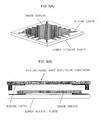
- FIG. 1(A) is a perspective view showing a lower support plate having wiring formed thereon.
- FIG. 1(B) is a view showing a state in which an electronic component, such as an image sensor (LSI chip), is mounted on and connected to the lower support plate.
- the image sensor is disposed with its light-receiving surface facing down.
- the lower support plate is separated from a wiring layer in a later step and has a wiring pattern formed thereon through electroforming, which will be described in detail later.
- An image sensor is disposed on the wiring pattern (wiring layer), and electrode terminals of the image sensor are electrically connected to the wiring pattern at required positions.
- an electronic component encompassing an image sensor is bonded onto the lower support plate having the wiring pattern by means of a die bonding material and is connected to the wiring pattern by means of bonding wires (wire bonding).
- the electronic component is flip-chip-mounted on the lower support plate having the wiring pattern.
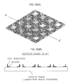
- FIGS. 2(A) and 2(B) are a pair of views showing in detail a first example of a wiring-added post electrode component integrally connected by a support plate, wherein FIG. 2(A) is a perspective view showing a unit pattern for use in a single semiconductor package, and FIG. 2(B) is a perspective view showing a connected pattern in which a plurality of patterns for use in a plurality of (16) semiconductor packages are connected together.
- the unit pattern or the connected pattern is configured such that a plurality of post electrodes with wiring are integrally connected by the support plate.
- the shape of a post electrode is not limited to a circular columnar shape as illustrated, but may be a columnar (rodlike) shape including a rectangular columnar shape, a polygonal columnar shape, etc.
- a central portion of the illustrated pattern is solid. However, the present invention is not limited thereto. A central portion of the pattern may be a cutout.
- a post-electrode-with-wiring pattern is manufactured through electroforming.
- Electroforming itself is well known. Electroforming is a "method of manufacturing, repairing, or replicating a metal product through electroplating," and is basically the same as electroplating. However, electroforming differs from electroplating in plating thickness, and also differs from electroplating in that an operation of separating a plating film is performed. Further, when a plating film is separated from a mother die and used, control and management of the physical properties of the plating film are important. A material including nickel, copper, a nickel alloy, or a copper alloy can be used as a plating metal (conductive material) to be deposited by electroforming. Stainless steel, which is a general conductive material, can be used as the material of the mother die.
- the mother die may be formed of a material composed of a base and a film covering the base.
- the base is formed of, for example, copper which does not greatly differ in coefficient of thermal expansion from a resin material used for resin sealing.
- the base is covered by, for example, a thin oxide film which allows passage of electricity for plating therethrough and which facilitates separation of a plating pattern.
- the composition of a plating bath and plating conditions must be selected such that no internal stress is produced. In the case of nickel plating, nickel sulfamate bath is used as a plating bath.
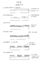
- FIG. 55 is a set of process charts showing a method of manufacturing an electroformed component by use of photoresist.
- photoresist nonconductive film
- a mother die of, for example, stainless steel
- the photoresist is exposed to light through a pattern film to thereby form a pattern, followed by development, whereby an original plate for electroforming is formed ((b) of FIG. 55 ).
- an original plate for electroforming is formed ((b) of FIG. 55 ).
- non-plating portions are covered by the photoresist pattern.
- the photoresist pattern has a thickness greater than the thickness of a resin-sealed semiconductor chip or the total thickness of a plurality of stacked chips; for example, a thickness of about 100 ⁇ m to 300 ⁇ m.
- a plating metal is deposited in opening portions of the photoresist pattern ( FIG. 55,(c) ). This is performed by use of a plating apparatus. An anode and a cathode are placed in a plating bath (e.g., nickel sulfamate solution) maintained at a proper temperature. The anode is formed of an electroforming metal to be deposited through electroforming.
- a plating bath e.g., nickel sulfamate solution
- the cathode is an electroforming mother die of, for example, stainless steel. As shown in (b) of FIG. 55 , a photoresist pattern is previously formed on the surface of the electroforming mother die serving as the cathode. When a current is caused to flow between the anode and the cathode, the electroforming metal of the anode melts, and is plated in the opening portions of the photoresist pattern on the electroforming mother die.
- the resist is removed ( FIG. 55,(e)) , whereby the plating metal forms post electrodes or a wiring pattern.
- the post electrodes formed by the plating metal are then separated from the electroforming mother die (FIG. 55,(f)). As will be described later, this separation process is performed after a resin sealing step (see FIG. 6 ).
- the feature of electroforming is that separation of the formed plating electrodes from a support plate can be readily performed by means of heat and pressure.
- a wiring layer and post electrodes are grown on a support plate (electroforming mother die) of a conductive material by use of lithography and plating, thereby forming a post-electrode-with-wiring pattern integral with the support plate.
- FIG. 3(A) is a perspective view showing a lower support plate on which an image sensor is mounted ( FIG. 1 ), and FIG. 3(B) is a sectional view showing a state in which a wiring-added post electrode component shown in FIG. 2(A) is disposed above the lower support plate. While the wiring layer formed on the lower support plate serves as a bonding pad region, an electronic component, such as an image sensor, is fixed and electrically connected to the wiring layer.
- FIG. 4 is a view showing a state in which the wiring-added post electrode component is connected to and fixed on the lower support plate.
- the wiring-added post electrode component integrally connected by an upper support plate is collectively fixed and electrically connected to a wiring pattern of the lower support plate at predetermined positions.
- Post electrodes can be fixed and connected by one of the following methods: (1) ultrasonic bonding; (2) connection by means of electrically conductive paste, such as silver paste; (3) connection by soldering; and (4) a method of forming recesses in metal pad portions for connection electrodes provided on an organic substrate, forming projections on the wiring-added post electrode component, and press-fitting the projections into the recesses, or inserting the projections into the recesses, followed by crimping.
- all of the post electrodes are integrally connected by the upper and lower support plates.
- FIG. 5 is a view showing a state in which, after fixation, resin sealing is performed.
- FIG. 5 shows only a single component; however, in actuality, a large number of components in a connected condition are placed in a mold, and resin is charged into the mold.
- transfer molding is performed so as to fill spaces between the upper and lower support plates with resin; alternatively, resin sealing is performed by use of a liquid resin (e.g., epoxy resin).
- a liquid resin e.g., epoxy resin
- FIG. 6 is a view showing a state after separation of the upper and lower support plates (electroforming mother dies). Separation of the support plates causes exposure of wiring layers on the upper and lower sides. Next, as shown in FIG. 7 , the resultant component is inverted (turned upside down).
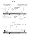
- a glass substrate is affixed on a front face side; i.e., on a side toward the light-receiving surface of the image sensor.
- the glass substrate or a transparent plate such as a transparent resin (acrylic, cycloolefin polymer, etc.) plate having good light transmittance, is affixed to a position from which the lower support plate has been separated.
- the transparent plate is affixed by use of an adhesive; for example, a thermosetting resin.
- the transparent plate may be affixed after singulation mentioned below.
- bump electrodes connected to the wiring layer are formed for external connection. At this time, if necessary, a protection film is applied onto the wiring layer on the back face.
- the positions of external electrodes of the image sensor chip can be shifted arbitrarily from the positions of the post electrodes. This readily enables three-dimensional connection of an image sensor chip package.
- FIG. 9(A) is a perspective view showing a glass substrate (or transparent resin substrate having good transmittance) having wiring formed thereon.
- FIG. 9(B) is a view showing a state in which an electronic component, such as an image sensor, is mounted on and connected to the glass substrate. The image sensor is disposed with a light-receiving surface facing down.
- FIGS. 9(A) and 9(B) uses the transparent glass substrate as a support plate.
- a metal seed layer which is to become a wiring pattern is formed on the entire surface of the transparent glass substrate (for example, a sputtering layer is formed, or a film is formed through application of a nanometal material).
- the seed layer can be, for example, a gold, silver, copper, or palladium foil, which allows copper plating thereon.
- a pattern of the wiring layer is formed by applying resist onto the seed layer, patterning through exposure, developing, etching, and removing the resist.
- a wiring layer is grown on the seed layer through plating.
- a seed layer pattern can be directly formed by use of nanometal particles, whereby a lithography process can be omitted. According to the direct patterning process, nanometal particles of copper or the like are contained in an organic solvent, and a required pattern is formed with the organic solvent by an ink jet method practically used in printers.
- FIG. 10(A) is a perspective view showing a state in which an image sensor is connected onto the glass substrate.
- FIG. 10(B) is a sectional view exemplifying a state in which the wiring-added post electrode component shown in FIG. 2(A) is disposed above the glass substrate. While the wiring layer formed on the glass substrate serves as a bonding pad region, an electronic component, such as an image sensor (semiconductor LSI chip), is fixed and electrically connected to the wiring layer.
- an image sensor semiconductor LSI chip
- FIG. 11 is a view showing a state in which the wiring-added post electrode component is fixed on and connected to the glass substrate. This connection is performed as mentioned previously with reference to FIG. 4 .
- FIG. 12 is a view showing a state in which, after fixation, resin sealing is performed. As mentioned previously with reference to FIG. 5 , transfer molding is performed so as to fill spaces between the glass substrate and an upper support plate with resin; alternatively, resin sealing is performed by use of a liquid resin (e.g., epoxy resin).
- a liquid resin e.g., epoxy resin
- FIG. 13 is a view showing a state after separation of the upper support plate. Separation of the upper support plate causes exposure of an upper wiring layer. Next, as shown in FIG. 14 , the resultant component is inverted (turned upside down).
- bump electrodes connected to the wiring layer are formed for external connection.
- a protection film is applied onto the wiring layer on the back face. Subsequently, singulation into individual chips is performed, thereby completing products.
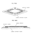
- FIG. 16(A) is a perspective view showing a lower support plate having wiring formed thereon.
- FIG. 16(B) is a sectional view showing a state in which an electronic component, such as an image sensor, is mounted on and connected to the lower support plate.
- FIGS. 16(A) and 16(B) are the same as FIGS. 1(A) and 1(B) , and the image sensor is mounted on and connected to the lower support plate having a wiring pattern formed thereon.
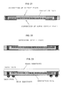
- FIGS. 17(A) and 17(B) are a pair of views showing a second example of a wiring-added post electrode component different from that shown in FIGS. 2(A) and 2(B) , wherein FIG. 17(A) is a perspective view showing a plurality of wiring-added post electrode components integrally connected together, and FIG. 17(B) is a sectional view taken along line Y-Y' of FIG. 17(A) .
- a lower support plate e.g., silicon substrate or glass
- the insulation tape is formed from an insulation material of a thin film and represented by a polyimide tape, etc.
- the insulation tape functions, in a completed product, as a protection film which covers a wiring layer.
- the lower support plate is separated from the insulation tape in a later step.
- a preliminary treatment is performed so as to facilitate separation of a silicon substrate (or glass) from the tape upon application of a temperature higher than, for example, a reflow temperature (the temperature is higher than a mold temperature).
- an adhesive which contains thermal capsules is used, or an adhesive which separates upon exposure to ultraviolet rays is used in combination with a support plate of a light-transmissive material (heat-resistant, low-thermal-expansion glass, etc.).
- a thermoplastic adhesive may be used.
- a metal seed layer which is to become a wiring pattern is formed on the tape, thereby forming a metal-coated tape.
- the seed layer may be, for example, a gold, silver, copper, or palladium foil, which allows copper plating thereon.
- a pattern of the wiring layer is formed by applying resist onto the seed layer, patterning through exposure, developing, etching, and removing the resist.
- a wiring layer is grown on the seed layer through plating.
- application of resist and development are performed on the wiring layer for forming post electrode portions, and post portions are grown through plating.
- a seed layer pattern can be directly formed by use of nanometal particles so as to form wiring portions, whereby a lithography process can be omitted.
- application of resist and development are performed on the wiring portions for forming post electrode portions, and post portions are grown through plating. By this procedure, the wiring-added post electrode components are completed.
- FIGS. 17(A) and 17(B) The wiring-added post electrode component shown in FIGS. 17(A) and 17(B) is fixed on and connected to the lower support plate of FIG. 16 on which image sensors are mounted.
- FIG. 18 exemplifies a state before connection.
- the post electrodes of each of the wiring-added post electrode components are fixed and electrically connected to a bonding pad region on the wiring layer.
- FIG. 19 is a view showing a state in which the wiring-added post electrode component is connected to and fixed on the lower support plate.
- FIG. 20 is a view showing a state in which, after fixation, resin sealing is performed. After the integrally connected wiring-added post electrode components are fixed on the lower support plate, the upper surfaces of the image sensors are transfer-molded with resin up to the lower surface of the insulation tape, or resin-sealed by use of a liquid resin (e.g., epoxy resin).
- a liquid resin e.g., epoxy resin
- FIG. 21 is a view showing a state after separation of the upper and lower support plates. For example, through application of a predetermined high temperature, the lower support plate is separated. The insulation tape which, by this procedure, is exposed upward in FIG. 21 functions as a protection film of completed products.
- FIG. 22 is a view showing a state after inversion (turning upside down).
- a glass substrate is affixed on a front face side; i.e., on a side toward the light-receiving surface of the image sensor.
- holes are formed in the insulation tape, and bump electrodes connected to the wiring exposed through openings of the holes are formed for external connection.
- the fourth embodiment uses a glass substrate having wiring formed thereon as exemplified in FIG. 9(A) .
- An electronic component such as an image sensor, is mounted on and connected to the glass substrate as exemplified in FIGS. 9(B) and 10(A) .
- the fourth embodiment uses such a glass substrate in combination with a wiring-added post electrode component having a 2-layer structure in which an insulation tape is affixed to the entire surface on one side of a support plate as exemplified in FIGS. 17(A) and 17(B) .
- FIG. 24 is a view showing a state in which the wiring-added post electrode component having the 2-layer structure support plate is disposed above the glass substrate on which the image sensor is mounted.
- FIG. 25 exemplifies a state in which the wiring-added post electrode component is connected to and fixed on the glass substrate on which the image sensor is mounted.
- the post electrodes of the wiring-added post electrode component are fixed and electrically connected to a bonding pad region on the wiring layer.
- the upper surfaces of the image sensors are transfer-molded with resin up to the lower surface of the insulation tape, or resin-sealed by use of a liquid resin (e.g., epoxy resin).
- a liquid resin e.g., epoxy resin
- FIG. 27 is a view showing a state after separation of the support plate. For example, through application of a predetermined high temperature or exposure to ultraviolet rays, the support plate is separated. The insulation tape which, by this procedure, is exposed upward in FIG. 27 functions as a protection film of completed products.
- FIG. 28 is a view showing a state after inversion (turning upside down).
- FIG. 29 on the back face side, holes are formed in the insulation tape, and bump electrodes connected to the wiring exposed through openings of the holes are formed for external connection.
- the semiconductor package of the fourth embodiment is completed.
- the fifth embodiment differs from the above-described first to fourth embodiments only in that, in place of the transparent glass substrate exemplified in the first to fourth embodiments, a highly heat-releasing substrate functioning as a heat sink, a heat spreader, or the like is used.
- FIGS. 30(A) and 30(B) are a pair of views showing a large number of wiring-added post electrode components of a third example integrally connected together, wherein FIG. 30(A) is a perspective view, and FIG. 30(B) is a sectional view taken along line X-X' of FIG. 30(A) .
- the third example shown in FIGS. 30(A) and 30(B) corresponds to the first example of a wiring-added post electrode component exemplified in FIGS. 2(A) and 2(B) , but differs in that a transparent glass substrate is used in place of the support plate of the first example.
- the wiring-added post electrode component of the third example is configured such that a plurality of post electrodes and wiring are integrally connected by the transparent glass substrate serving as a back support plate.
- a metal seed layer which is to become a wiring pattern is formed on the entire surface of the transparent glass substrate (for example, a sputtering layer is formed, or a film is formed through application of a nanometal material).
- the seed layer may be, for example, a gold, silver, copper, or palladium foil, which allows copper plating thereon.
- a pattern of the wiring layer is formed by applying resist onto the seed layer, patterning through exposure, developing, etching, and removing the resist.
- a wiring layer is grown on the seed layer through plating. Furthermore, application of resist and development are performed on the wiring layer for forming post electrode portions, and post portions are grown through plating.
- a seed layer pattern can be directly formed by use of nanometal particles, whereby a lithography process can be omitted.
- nanometal particles of copper or the like are contained in an organic solvent, and a required pattern is formed with the organic solvent by an ink jet method practically used in printers.
- application of resist and development are performed on the seed layer pattern for forming post electrode portions, and post portions are grown through plating. By this procedure, the wiring-added post electrode components are completed.
- FIG. 31 exemplifies a state in which an image sensor (semiconductor LSI chip) is mounted on a wiring-added post electrode component. While the wiring layer formed on the wiring-added post electrode component serves as a bonding pad region, the image sensor (semiconductor LSI chip) is fixed and electrically connected to the wiring layer. The fixation and connection can be performed through flip-chip bonding. Also, a microlens can be mounted between the glass substrate and the light-receiving surface of the image sensor. In this manner, the image sensor is mounted on the back face side of the transparent glass substrate.
- FIG. 32 is a view showing a state in which, after the semiconductor LSI chip has been connected and fixed to the wiring-added post electrode component, resin sealing is performed.
- FIG. 32 shows only a single component; however, in actuality, a large number of components in a connected condition are placed in a mold, and resin is charged into the mold.
- transfer molding is performed so as to fill spaces between the ends of the electrode posts and the transparent glass substrate with resin; alternatively, resin sealing is performed by use of a liquid resin (e.g., epoxy resin).
- a liquid resin e.g., epoxy resin
- FIG. 33 is a view showing a state after formation of bump electrodes for external connection.
- the post electrode ends exposed from a resin seal portion can be used as external electrodes, as shown in FIG. 33 , the bump electrodes connected to the post electrode ends may be formed for use as external electrodes.
- singulation into individual chips is performed through cutting, thereby completing products.
- image sensor chip package in which the bump electrodes serving as external electrodes are formed on a side opposite the transparent glass substrate without need to use through electrodes as practiced conventionally.
- the thus-completed image sensor chip packages can be readily connected to other packages, such as signal-processing LSI chip packages.
- FIGS. 34 and 35 are schematic sectional views showing a state in which the image sensor chip package before formation of bump electrodes exemplified in FIG. 32 is bonded to a signal-processing LSI chip package in a layered manner.
- FIG. 34 shows a state before connection
- FIG. 35 shows a state after connection.
- the signal-processing LSI chip package is configured as a dual face package (PKG).
- PKG dual face package
- the upper image sensor chip package is aligned with the lower signal-processing LSI chip package for alignment of connection portions.
- the thus-aligned packages are caused to pass through a furnace for momentarily melting projecting electrodes (post electrodes) of the connection portions through application of heat, thereby establishing connections.
- the image sensor chip package shown in FIGS. 34 and 35 is manufactured as have been described previously with reference to FIGS. 30 to 33 .
- Manufacture of a dual face package, such as a signal-processing LSI (logic LSI) chip package, will be sequentially described with reference to FIGS. 36 to 41 .
- FIG. 36 is a view showing a state in which an LSI chip (signal-processing LSI chip) is bonded onto and connected to a multilayer organic substrate.
- the LSI chip is exemplified in such a manner as to be bonded onto the multilayer substrate by means of a die bonding material and connected to a top-layer wiring pattern of the organic substrate by means of bonding wires.
- the top-layer wiring pattern of a multilayer or single-layer organic substrate has metal pad portions for bonding which are to become bonding wire connection electrodes, and wiring to the metal pad portions.
- Au bonding wires are used to connect the LSI chip and the metal pad portions on the front face of the multilayer or single-layer organic substrate.
- the LSI chip can be connected to the organic substrate through flip-chip bonding (not shown).
- the LSI chip is connected to the top-layer wiring pattern of the multilayer or single-layer organic substrate by a conventional flip-chip bonding technique.
- the single-layer organic substrate employs a single-layer 2-layer-wiring structure.
- the multilayer organic substrate is formed by forming a wiring pattern on each of a plurality of substrates, bonding the substrates together in layers, and, as needed, forming through holes for connecting the wiring patterns of different layers. Conductor layers are formed in the through holes and connected to lands formed on the back face side and serving as end surface electrode portions.
- Such a multilayer or single-layer organic substrate is known as, for example, a collectively sealed organic substrate in which small balls (bumps) of a solder material called "solder balls" are formed on the back face (BGA: Ball Grid Array).
- FIG. 37 is a view showing a state in which post electrodes are fixed and connected.
- a post electrode component integrally connected by a support plate is collectively fixed and electrically connected to a wiring pattern of the organic substrate at predetermined positions.
- the post electrodes can be fixed and connected by one of the following methods: (1) ultrasonic bonding; (2) connection by means of electrically conductive paste, such as silver paste; (3) connection by soldering; and (4) a method of forming recesses in metal pad portions for connection electrodes provided on the organic substrate, forming projections on the post electrode component, and press-fitting the projections into the recesses, or inserting the projections into the recesses, followed by crimping.
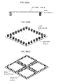
- FIGS. 38(A), 38(B) and 38(C) are a set of views showing in detail a post electrode component integrally connected by a support plate, wherein FIGS. 38(A) and 38(B) are a sectional view and a perspective view, respectively, showing a unit pattern for use in a single dual face package, and FIG. 38(C) is a perspective view showing a single connected pattern in which four unit patterns are integrally connected together, for use in four dual face packages.
- the post electrode component is configured similar to the above-described first to third examples of a wiring-added post electrode component, but differs in that a wiring pattern is not provided as shown in FIGS. 38(A) to 38(C) .
- the post electrode component of FIGS. 38(A) to 38(C) is configured such that a plurality of post electrodes are integrally connected by the support plate.
- the integrally connected post electrode component is manufactured through electroforming which has been described with reference to FIG. 55 .
- FIG. 39 is a view showing a state in which, after the post electrode component has been connected to and fixed on the multilayer organic substrate, resin sealing is performed.
- the front surfaces of LSI chips are transfer-molded with resin up to the lower surface of the support plate (electroforming mother die); i.e., transfer molding is performed so as to fill a space between the LSI chips and the support plate with resin; alternatively, resin sealing is performed by use of a liquid resin (e.g., epoxy resin).
- a liquid resin e.g., epoxy resin
- FIG. 40 is a view showing a state after separation of the support plate (electroforming mother die). Separation of the support plate electrically separates a plurality of post electrodes from one another.
- FIG. 41 is a view showing a state after formation of bump electrodes for external connection formed on the back face.
- the ends of the post electrodes can be used as external electrodes to be connected to the aforementioned image sensor chip package.
- electrode positions can be shifted arbitrarily from post electrode positions to external electrode positions of the image sensor chip. This readily enables three-dimensional connection of an image sensor chip package.
- Rewiring can be performed by means of ink jet printing or screen printing. Alternatively, for rewiring, electroless plating can be performed after formation of a seed layer pattern. Also, rewiring can be performed by use of the first example of a wiring-added post electrode component which has been described with reference to FIGS. 2(A) and 2(B) .
- a wiring-added post electrode component not only post electrodes supported by a support plate but also a wiring pattern connected to the post electrodes and serving as an upper-face wiring pattern are formed through electroforming.
- the wiring-added post electrode component of the first example is fixed on and electrically connected to the multilayer organic substrate (see FIG. 36 ) having the LSI chip bonded and connected thereto.
- a subsequent process can be similar to the process which has been described with reference to FIGS. 37 to 40 .
- FIGS. 42(A) and 42(B) are a pair of views showing a large number of wiring-added post electrode components of a fourth example integrally connected together, wherein FIG. 42(A) is a perspective view, and FIG. 42(B) is a sectional view taken along line Y-Y' of FIG. 42(A) .
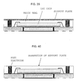
- the configuration of the wiring-added post electrode components of the fourth example shown in FIG. 42 differs from that shown in FIGS. 30(A) and 30(B) only in that, in place of the transparent glass substrate exemplified above in FIGS. 30(A) and 30(B) , a highly heat-releasing substrate functioning as a heat sink, a heat spreader, or the like is used.
- An example method of manufacturing the wiring-added post electrode components exemplified in FIGS. 42(A) and 42(B) is as follows. First, a thin insulation layer is provided on a highly heat-releasing substrate. Subsequently, similar to the case of FIGS. 30(A) and 30(B) , a metal seed layer is formed on the entire surface of the highly heat-releasing substrate (for example, a sputtering layer is formed, or a film is formed through application of a nanometal material). Then, resist is applied onto the seed layer, and a wiring pattern is formed through development, followed by growing through plating. Subsequently, for formation of post portions, application of resist and development are performed, followed by growing through plating. Thus, a plurality of post electrodes and wiring patterns are configured in such a manner as to be integrally connected together by the highly heat-releasing substrate serving as a back support plate.
- FIG. 43 exemplifies a state in which a high-power LSI chip is attached to the wiring-added post electrode component.
- the high-power LSI chip which requires intensive release of heat is fixed and electrically connected to the wiring-added post electrode component having the highly heat-releasing substrate.
- the highly heat-generating LSI chip is mounted on the back face side of the highly heat-releasing substrate functioning as a heat sink.
- FIG. 44 is a view showing a state in which, after the high-power LSI chip has been connected and fixed to the wiring-added post electrode component, resin sealing is performed. Transfer molding is performed so as to fill a space between the ends of the electrode posts and the lower surface of the highly heat-releasing substrate with resin; alternatively, resin sealing is performed by use of a liquid resin (e.g., epoxy resin).
- a liquid resin e.g., epoxy resin
- FIG. 45 is a view showing a state after formation of bump electrodes for external connection.
- Post electrode ends exposed from a resin seal portion can be used as external electrodes.
- bump electrodes connected to the post electrode ends can be formed for use as external connection electrodes.
- FIGS. 46 and 47 are schematic sectional views showing a state in which the high-power LSI chip package before formation of bump electrodes shown in FIG. 44 is bonded to another low-power LSI chip package in a layered manner.
- FIG. 46 shows a state before connection
- FIG. 47 shows a state after connection.
- the low-power LSI chip package is configured as a dual face package (PKG).
- the low-power LSI chip package can have a configuration similar to that having been described with reference to FIGS. 36 to 41 . Similar to the previously described configuration, rewiring may be formed on the upper surface of the LSI package.
- FIG. 46 is a view showing a state after connection of the LSI packages.
- FIG. 48 is a view showing a state in which still another LSI chip package is additionally layered. Even in the case of three or more layers, an LSI having the greatest power consumption is disposed as a top layer.
- An illustrated first package corresponds to the high-power LSI chip package having a highly heat-releasing substrate exemplified in FIG. 45 .
- Illustrated second and third packages correspond to the above-mentioned low-power LSI chip package.
- the size of a heat releasing portion is not limited to the size of the entire surface of a package, but can be determined arbitrarily.
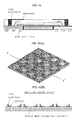
- FIGS. 49(A), 49(B) and 49(C) are a set of views exemplifying a state in which an image sensor (or high-power LSI chip package) is attached to a wiring-added post electrode component, wherein FIG. 49(A) is a sectional view, FIG. 49(B) is a perspective view of a wiring-added post electrode component as viewed from the back side, and FIG.
- FIGS. 49(A), 49(B) and 49(C) are a perspective view, as viewed from the back side, of the post-electrode-with-wiring to which the image sensor is attached.
- FIGS. 49(A), 49(B) and 49(C) correspond to aforementioned FIG. 31 or FIG. 43 , but differs only in that, in place of the aforementioned glass substrate or highly heat-releasing substrate, a separable support plate (electroforming mother die) is used.
- the wiring-added post electrode component shown in FIG. 49(B) can be manufactured similar to manufacture of the wiring-added post electrode component of the first example which has been described with reference to FIGS. 2A and 2(B) .
- the support plate shown in FIGS. 49(A) to 49(C) is separated in a later step.
- FIG. 50 is a view showing a state in which, after a semiconductor LSI chip has been connected and fixed to the wiring-added post electrode component, resin sealing is performed.
- FIG. 51 is a view showing a state after separation of the support plate.
- the support plate formed through electroforming can be readily separated. Separation of the support plate electrically separates a plurality of post electrodes from one another.
- FIG. 52 is a view showing a state in which a glass substrate or a transparent resin (acrylic, cycloolefin polymer, etc.) substrate having good light transmittance, or a highly heat-releasing substrate is affixed to a position from which the support plate has been separated.
- the substrate is affixed by use of an adhesive; for example, a thermosetting resin.
- the substrate may be affixed after singulation mentioned below.
- FIG. 53 is a view showing a state after formation of bump electrodes for external connection.
- Post electrode ends exposed from a resin seal portion can be used as external electrodes.
- bump electrodes connected to the post electrode ends can be formed for use as external electrodes. In actual manufacture, subsequently, singulation into individual chips is performed through cutting, thereby completing products.
Landscapes
- Engineering & Computer Science (AREA)
- Manufacturing & Machinery (AREA)
- Microelectronics & Electronic Packaging (AREA)
- Solid State Image Pick-Up Elements (AREA)
Applications Claiming Priority (2)
| Application Number | Priority Date | Filing Date | Title |
|---|---|---|---|
| JP2008020775A JP5690466B2 (ja) | 2008-01-31 | 2008-01-31 | 半導体チップパッケージの製造方法 |
| PCT/JP2009/050530 WO2009096240A1 (ja) | 2008-01-31 | 2009-01-16 | 半導体チップパッケージ及びその製造方法 |
Publications (3)
| Publication Number | Publication Date |
|---|---|
| EP2239773A1 true EP2239773A1 (de) | 2010-10-13 |
| EP2239773A4 EP2239773A4 (de) | 2017-04-26 |
| EP2239773B1 EP2239773B1 (de) | 2022-06-22 |
Family
ID=40912593
Family Applications (1)
| Application Number | Title | Priority Date | Filing Date |
|---|---|---|---|
| EP09707063.5A Active EP2239773B1 (de) | 2008-01-31 | 2009-01-16 | Herstellungsverfahren für halbleiter-chippaket |
Country Status (5)
| Country | Link |
|---|---|
| US (1) | US8110911B2 (de) |
| EP (1) | EP2239773B1 (de) |
| JP (1) | JP5690466B2 (de) |
| KR (1) | KR101150322B1 (de) |
| WO (1) | WO2009096240A1 (de) |
Cited By (2)
| Publication number | Priority date | Publication date | Assignee | Title |
|---|---|---|---|---|
| EP2472579A1 (de) * | 2010-12-30 | 2012-07-04 | Baumer Innotec AG | Kontaktierung von Bauelementen auf Substraten |
| US10714402B2 (en) | 2016-06-20 | 2020-07-14 | Sony Corporation | Semiconductor chip package for improving freedom of arrangement of external terminals |
Families Citing this family (30)
| Publication number | Priority date | Publication date | Assignee | Title |
|---|---|---|---|---|
| KR101009103B1 (ko) * | 2008-10-27 | 2011-01-18 | 삼성전기주식회사 | 양면 전극 패키지 및 그 제조방법 |
| JP5665020B2 (ja) * | 2009-12-22 | 2015-02-04 | 国立大学法人九州工業大学 | 配線用電子部品の製造方法 |
| JP2012044091A (ja) * | 2010-08-23 | 2012-03-01 | Canon Inc | 撮像装置、撮像モジュール及びカメラ |
| KR101163222B1 (ko) | 2010-09-13 | 2012-07-06 | 에스케이하이닉스 주식회사 | 반도체 패키지 및 그 제조방법 |
| US9142502B2 (en) | 2011-08-31 | 2015-09-22 | Zhiwei Gong | Semiconductor device packaging having pre-encapsulation through via formation using drop-in signal conduits |
| US8916421B2 (en) * | 2011-08-31 | 2014-12-23 | Freescale Semiconductor, Inc. | Semiconductor device packaging having pre-encapsulation through via formation using lead frames with attached signal conduits |
| US8597983B2 (en) | 2011-11-18 | 2013-12-03 | Freescale Semiconductor, Inc. | Semiconductor device packaging having substrate with pre-encapsulation through via formation |
| CN103794592B (zh) * | 2012-10-30 | 2016-10-05 | 中芯国际集成电路制造(上海)有限公司 | 具有接地屏蔽结构的半导体器件 |
| JP2016027586A (ja) * | 2012-11-29 | 2016-02-18 | パナソニック株式会社 | 光学装置および光学装置の製造方法 |
| WO2014083750A1 (ja) | 2012-11-30 | 2014-06-05 | パナソニック株式会社 | 光学装置及びその製造方法 |
| TWM455258U (zh) * | 2013-01-11 | 2013-06-11 | 勝開科技股份有限公司 | 具有氣室缺口之影像感測器結構 |
| KR20140126598A (ko) * | 2013-04-23 | 2014-10-31 | 삼성전자주식회사 | 반도체 패키지 및 그 제조 방법 |
| JP2015064413A (ja) * | 2013-09-24 | 2015-04-09 | 富士通株式会社 | 光半導体素子とその製造方法 |
| JP6327140B2 (ja) * | 2014-12-15 | 2018-05-23 | 株式会社デンソー | 電子装置 |
| KR20180054799A (ko) * | 2015-11-27 | 2018-05-24 | 차이나 와퍼 레벨 씨에스피 씨오., 엘티디. | 이미지 감지 칩 패키징 구조 및 방법 |
| US10153224B2 (en) * | 2016-09-14 | 2018-12-11 | Globalfoundries Inc. | Backside spacer structures for improved thermal performance |
| US10804115B2 (en) * | 2017-08-03 | 2020-10-13 | General Electric Company | Electronics package with integrated interconnect structure and method of manufacturing thereof |
| US10541153B2 (en) | 2017-08-03 | 2020-01-21 | General Electric Company | Electronics package with integrated interconnect structure and method of manufacturing thereof |
| US10541209B2 (en) | 2017-08-03 | 2020-01-21 | General Electric Company | Electronics package including integrated electromagnetic interference shield and method of manufacturing thereof |
| CN110139461A (zh) * | 2018-02-02 | 2019-08-16 | 三赢科技(深圳)有限公司 | 电路板、电路板的形成方法及相机模组 |
| CN112189260A (zh) * | 2018-05-28 | 2021-01-05 | 索尼半导体解决方案公司 | 成像装置 |
| CN109346534B (zh) * | 2018-11-23 | 2024-05-07 | 中国电子科技集团公司第四十四研究所 | 一种陶瓷管壳结构及其封装结构 |
| US12010416B1 (en) * | 2019-09-27 | 2024-06-11 | Apple Inc. | Camera module including embedded ceramic substrate package |
| KR20210155455A (ko) * | 2020-06-16 | 2021-12-23 | 삼성전자주식회사 | 반도체 패키지 |
| WO2022029969A1 (ja) * | 2020-08-06 | 2022-02-10 | オリンパス株式会社 | 撮像ユニット、挿入機器 |
| KR102890788B1 (ko) | 2020-11-23 | 2025-11-26 | 삼성전자주식회사 | 글래스 기판을 포함하는 이미지 센서 패키지 |
| CN113488490A (zh) * | 2021-06-07 | 2021-10-08 | 季华实验室 | 基于穿塑通孔的cis板级扇出型封装结构及其制作方法 |
| US12035060B2 (en) * | 2021-11-05 | 2024-07-09 | Omnivision Technologies, Inc. | Stacked image sensor |
| CN114725144B (zh) * | 2022-04-06 | 2025-07-29 | 三星半导体(中国)研究开发有限公司 | 制造半导体封装件的方法、半导体封装件及成像设备 |
| CN117410238B (zh) * | 2023-12-14 | 2024-09-13 | 青岛泰睿思微电子有限公司 | 内埋芯片的打线种球封装结构 |
Family Cites Families (22)
| Publication number | Priority date | Publication date | Assignee | Title |
|---|---|---|---|---|
| US6538210B2 (en) * | 1999-12-20 | 2003-03-25 | Matsushita Electric Industrial Co., Ltd. | Circuit component built-in module, radio device having the same, and method for producing the same |
| JP3772066B2 (ja) * | 2000-03-09 | 2006-05-10 | 沖電気工業株式会社 | 半導体装置 |
| JP2002134653A (ja) * | 2000-10-23 | 2002-05-10 | Matsushita Electric Ind Co Ltd | 半導体装置とその製造方法 |
| JP2003229513A (ja) * | 2001-11-29 | 2003-08-15 | Sony Corp | 素子内蔵基板および素子内蔵基板の製造方法 |
| TW200302685A (en) * | 2002-01-23 | 2003-08-01 | Matsushita Electric Industrial Co Ltd | Circuit component built-in module and method of manufacturing the same |
| US6885107B2 (en) * | 2002-08-29 | 2005-04-26 | Micron Technology, Inc. | Flip-chip image sensor packages and methods of fabrication |
| JP4126389B2 (ja) * | 2002-09-20 | 2008-07-30 | カシオ計算機株式会社 | 半導体パッケージの製造方法 |
| JP3740469B2 (ja) * | 2003-01-31 | 2006-02-01 | 株式会社東芝 | 半導体装置および半導体装置の製造方法 |
| JP2005039227A (ja) * | 2003-07-03 | 2005-02-10 | Matsushita Electric Ind Co Ltd | 半導体内蔵モジュールとその製造方法 |
| US7141884B2 (en) * | 2003-07-03 | 2006-11-28 | Matsushita Electric Industrial Co., Ltd. | Module with a built-in semiconductor and method for producing the same |
| JP3938921B2 (ja) * | 2003-07-30 | 2007-06-27 | Tdk株式会社 | 半導体ic内蔵モジュールの製造方法 |
| JP2005236039A (ja) * | 2004-02-19 | 2005-09-02 | Tdk Corp | 半導体ic内蔵基板及びその製造方法、並びに、半導体ic内蔵モジュール |
| JP2005294320A (ja) * | 2004-03-31 | 2005-10-20 | Sanyo Electric Co Ltd | 半導体装置およびその製造方法 |
| JP2006049822A (ja) * | 2004-06-29 | 2006-02-16 | Tdk Corp | 半導体ic内蔵モジュール |
| DE102004046227B3 (de) * | 2004-09-22 | 2006-04-20 | Infineon Technologies Ag | Verfahren zur Herstellung eines Halbleiterbauteils mit Durchkontakten durch eine Kunststoffgehäusemasse und entsprechendes Halbleiterbauteil |
| JP2006128625A (ja) * | 2004-09-30 | 2006-05-18 | Oki Electric Ind Co Ltd | 半導体装置及びその製造方法 |
| JP2006129625A (ja) | 2004-10-29 | 2006-05-18 | Konica Minolta Opto Inc | 駆動装置 |
| JP2006165252A (ja) * | 2004-12-07 | 2006-06-22 | Shinko Electric Ind Co Ltd | チップ内蔵基板の製造方法 |
| JP4837328B2 (ja) * | 2005-08-01 | 2011-12-14 | 新光電気工業株式会社 | 半導体装置及び半導体装置の製造方法 |
| JP4764710B2 (ja) * | 2005-12-06 | 2011-09-07 | 株式会社ザイキューブ | 半導体装置とその製造方法 |
| JP4498336B2 (ja) * | 2006-10-16 | 2010-07-07 | Okiセミコンダクタ株式会社 | 半導体装置および半導体装置の製造方法 |
| WO2008065896A1 (en) * | 2006-11-28 | 2008-06-05 | Kyushu Institute Of Technology | Method for manufacturing semiconductor device having dual-face electrode structure and semiconductor device manufactured by the method |
-
2008
- 2008-01-31 JP JP2008020775A patent/JP5690466B2/ja active Active
-
2009
- 2009-01-16 EP EP09707063.5A patent/EP2239773B1/de active Active
- 2009-01-16 US US12/864,125 patent/US8110911B2/en active Active
- 2009-01-16 WO PCT/JP2009/050530 patent/WO2009096240A1/ja not_active Ceased
- 2009-01-16 KR KR1020107014511A patent/KR101150322B1/ko active Active
Cited By (2)
| Publication number | Priority date | Publication date | Assignee | Title |
|---|---|---|---|---|
| EP2472579A1 (de) * | 2010-12-30 | 2012-07-04 | Baumer Innotec AG | Kontaktierung von Bauelementen auf Substraten |
| US10714402B2 (en) | 2016-06-20 | 2020-07-14 | Sony Corporation | Semiconductor chip package for improving freedom of arrangement of external terminals |
Also Published As
| Publication number | Publication date |
|---|---|
| US20100295178A1 (en) | 2010-11-25 |
| JP2009182208A (ja) | 2009-08-13 |
| KR20100089894A (ko) | 2010-08-12 |
| US8110911B2 (en) | 2012-02-07 |
| JP5690466B2 (ja) | 2015-03-25 |
| WO2009096240A1 (ja) | 2009-08-06 |
| EP2239773A4 (de) | 2017-04-26 |
| EP2239773B1 (de) | 2022-06-22 |
| KR101150322B1 (ko) | 2012-06-08 |
Similar Documents
| Publication | Publication Date | Title |
|---|---|---|
| US8110911B2 (en) | Semiconductor chip package with post electrodes | |
| US8415789B2 (en) | Three-dimensionally integrated semicondutor device and method for manufacturing the same | |
| US8017452B2 (en) | Method of manufacturing semiconductor device with electrode for external connection and semiconductor device obtained by means of said method | |
| US10748840B2 (en) | Chip-size, double side connection package and method for manufacturing the same | |
| EP2261974B1 (de) | Elektronisches bauteil für die verkabelung und sein herstellungsverfahren | |
| JP2009070882A (ja) | 半導体チップパッケージ及びその製造方法 | |
| JP2005033141A (ja) | 半導体装置及びその製造方法、疑似ウェーハ及びその製造方法、並びに半導体装置の実装構造 | |
| JP7257463B2 (ja) | 埋め込み構造およびその作製方法ならびに基板 | |
| TW201123391A (en) | Lead frame and manufacturing method of the same | |
| JP2009021267A (ja) | 外部接続用電極を配置した半導体装置及びその製造方法 | |
| JP2009059771A (ja) | ウエハレベルチップサイズパッケージ及びその製造方法 | |
| WO2025220084A1 (ja) | 半導体装置の製造方法、該半導体装置の製造方法に用いられる接合材及びキャリア、並びに、半導体装置 |
Legal Events
| Date | Code | Title | Description |
|---|---|---|---|
| PUAI | Public reference made under article 153(3) epc to a published international application that has entered the european phase |
Free format text: ORIGINAL CODE: 0009012 |
|
| 17P | Request for examination filed |
Effective date: 20100712 |
|
| AK | Designated contracting states |
Kind code of ref document: A1 Designated state(s): AT BE BG CH CY CZ DE DK EE ES FI FR GB GR HR HU IE IS IT LI LT LU LV MC MK MT NL NO PL PT RO SE SI SK TR |
|
| AX | Request for extension of the european patent |
Extension state: AL BA RS |
|
| DAX | Request for extension of the european patent (deleted) | ||
| RAP1 | Party data changed (applicant data changed or rights of an application transferred) |
Owner name: INVENSAS CORPORATION |
|
| RA4 | Supplementary search report drawn up and despatched (corrected) |
Effective date: 20170327 |
|
| RIC1 | Information provided on ipc code assigned before grant |
Ipc: H01L 21/683 20060101ALI20170321BHEP Ipc: H05K 1/02 20060101ALN20170321BHEP Ipc: H01L 27/14 20060101ALI20170321BHEP Ipc: H01L 27/146 20060101ALI20170321BHEP Ipc: H01L 31/0203 20140101ALI20170321BHEP Ipc: H01L 23/538 20060101AFI20170321BHEP Ipc: H01L 25/16 20060101ALI20170321BHEP Ipc: H01L 23/00 20060101ALI20170321BHEP Ipc: H05K 1/18 20060101ALI20170321BHEP |
|
| STAA | Information on the status of an ep patent application or granted ep patent |
Free format text: STATUS: EXAMINATION IS IN PROGRESS |
|
| 17Q | First examination report despatched |
Effective date: 20200116 |
|
| RIC1 | Information provided on ipc code assigned before grant |
Ipc: H05K 1/18 20060101AFI20210514BHEP Ipc: H01L 23/538 20060101ALI20210514BHEP Ipc: H01L 23/00 20060101ALI20210514BHEP Ipc: H01L 21/683 20060101ALI20210514BHEP Ipc: H01L 25/16 20060101ALI20210514BHEP Ipc: H01L 27/14 20060101ALI20210514BHEP Ipc: H01L 31/0203 20140101ALI20210514BHEP Ipc: H01L 27/146 20060101ALI20210514BHEP Ipc: H01L 21/56 20060101ALI20210514BHEP Ipc: H05K 1/02 20060101ALN20210514BHEP |
|
| GRAP | Despatch of communication of intention to grant a patent |
Free format text: ORIGINAL CODE: EPIDOSNIGR1 |
|
| STAA | Information on the status of an ep patent application or granted ep patent |
Free format text: STATUS: GRANT OF PATENT IS INTENDED |
|
| RIC1 | Information provided on ipc code assigned before grant |
Ipc: H05K 1/18 20060101AFI20210617BHEP Ipc: H01L 23/538 20060101ALI20210617BHEP Ipc: H01L 23/00 20060101ALI20210617BHEP Ipc: H01L 21/683 20060101ALI20210617BHEP Ipc: H01L 25/16 20060101ALI20210617BHEP Ipc: H01L 27/14 20060101ALI20210617BHEP Ipc: H01L 31/0203 20140101ALI20210617BHEP Ipc: H01L 27/146 20060101ALI20210617BHEP Ipc: H01L 21/56 20060101ALI20210617BHEP Ipc: H05K 1/02 20060101ALN20210617BHEP |
|
| INTG | Intention to grant announced |
Effective date: 20210709 |
|
| GRAJ | Information related to disapproval of communication of intention to grant by the applicant or resumption of examination proceedings by the epo deleted |
Free format text: ORIGINAL CODE: EPIDOSDIGR1 |
|
| STAA | Information on the status of an ep patent application or granted ep patent |
Free format text: STATUS: EXAMINATION IS IN PROGRESS |
|
| REG | Reference to a national code |
Ref country code: DE Ref legal event code: R079 Ref document number: 602009064489 Country of ref document: DE Free format text: PREVIOUS MAIN CLASS: H01L0023120000 Ipc: H05K0001180000 |
|
| INTC | Intention to grant announced (deleted) | ||
| RIC1 | Information provided on ipc code assigned before grant |
Ipc: H05K 1/02 20060101ALN20211125BHEP Ipc: H01L 21/56 20060101ALI20211125BHEP Ipc: H01L 27/146 20060101ALI20211125BHEP Ipc: H01L 31/0203 20140101ALI20211125BHEP Ipc: H01L 27/14 20060101ALI20211125BHEP Ipc: H01L 25/16 20060101ALI20211125BHEP Ipc: H01L 21/683 20060101ALI20211125BHEP Ipc: H01L 23/00 20060101ALI20211125BHEP Ipc: H01L 23/538 20060101ALI20211125BHEP Ipc: H05K 1/18 20060101AFI20211125BHEP |
|
| GRAP | Despatch of communication of intention to grant a patent |
Free format text: ORIGINAL CODE: EPIDOSNIGR1 |
|
| STAA | Information on the status of an ep patent application or granted ep patent |
Free format text: STATUS: GRANT OF PATENT IS INTENDED |
|
| INTG | Intention to grant announced |
Effective date: 20220113 |
|
| GRAS | Grant fee paid |
Free format text: ORIGINAL CODE: EPIDOSNIGR3 |
|
| GRAA | (expected) grant |
Free format text: ORIGINAL CODE: 0009210 |
|
| STAA | Information on the status of an ep patent application or granted ep patent |
Free format text: STATUS: THE PATENT HAS BEEN GRANTED |
|
| AK | Designated contracting states |
Kind code of ref document: B1 Designated state(s): AT BE BG CH CY CZ DE DK EE ES FI FR GB GR HR HU IE IS IT LI LT LU LV MC MK MT NL NO PL PT RO SE SI SK TR |
|
| REG | Reference to a national code |
Ref country code: GB Ref legal event code: FG4D |
|
| REG | Reference to a national code |
Ref country code: CH Ref legal event code: EP |
|
| REG | Reference to a national code |
Ref country code: DE Ref legal event code: R096 Ref document number: 602009064489 Country of ref document: DE |
|
| REG | Reference to a national code |
Ref country code: AT Ref legal event code: REF Ref document number: 1500655 Country of ref document: AT Kind code of ref document: T Effective date: 20220715 |
|
| REG | Reference to a national code |
Ref country code: IE Ref legal event code: FG4D |
|
| REG | Reference to a national code |
Ref country code: NL Ref legal event code: FP |
|
| REG | Reference to a national code |
Ref country code: LT Ref legal event code: MG9D |
|
| PG25 | Lapsed in a contracting state [announced via postgrant information from national office to epo] |
Ref country code: SE Free format text: LAPSE BECAUSE OF FAILURE TO SUBMIT A TRANSLATION OF THE DESCRIPTION OR TO PAY THE FEE WITHIN THE PRESCRIBED TIME-LIMIT Effective date: 20220622 Ref country code: NO Free format text: LAPSE BECAUSE OF FAILURE TO SUBMIT A TRANSLATION OF THE DESCRIPTION OR TO PAY THE FEE WITHIN THE PRESCRIBED TIME-LIMIT Effective date: 20220922 Ref country code: LT Free format text: LAPSE BECAUSE OF FAILURE TO SUBMIT A TRANSLATION OF THE DESCRIPTION OR TO PAY THE FEE WITHIN THE PRESCRIBED TIME-LIMIT Effective date: 20220622 Ref country code: HR Free format text: LAPSE BECAUSE OF FAILURE TO SUBMIT A TRANSLATION OF THE DESCRIPTION OR TO PAY THE FEE WITHIN THE PRESCRIBED TIME-LIMIT Effective date: 20220622 Ref country code: GR Free format text: LAPSE BECAUSE OF FAILURE TO SUBMIT A TRANSLATION OF THE DESCRIPTION OR TO PAY THE FEE WITHIN THE PRESCRIBED TIME-LIMIT Effective date: 20220923 Ref country code: FI Free format text: LAPSE BECAUSE OF FAILURE TO SUBMIT A TRANSLATION OF THE DESCRIPTION OR TO PAY THE FEE WITHIN THE PRESCRIBED TIME-LIMIT Effective date: 20220622 Ref country code: BG Free format text: LAPSE BECAUSE OF FAILURE TO SUBMIT A TRANSLATION OF THE DESCRIPTION OR TO PAY THE FEE WITHIN THE PRESCRIBED TIME-LIMIT Effective date: 20220922 |
|
| REG | Reference to a national code |
Ref country code: AT Ref legal event code: MK05 Ref document number: 1500655 Country of ref document: AT Kind code of ref document: T Effective date: 20220622 |
|
| PG25 | Lapsed in a contracting state [announced via postgrant information from national office to epo] |
Ref country code: LV Free format text: LAPSE BECAUSE OF FAILURE TO SUBMIT A TRANSLATION OF THE DESCRIPTION OR TO PAY THE FEE WITHIN THE PRESCRIBED TIME-LIMIT Effective date: 20220622 |
|
| PG25 | Lapsed in a contracting state [announced via postgrant information from national office to epo] |
Ref country code: SK Free format text: LAPSE BECAUSE OF FAILURE TO SUBMIT A TRANSLATION OF THE DESCRIPTION OR TO PAY THE FEE WITHIN THE PRESCRIBED TIME-LIMIT Effective date: 20220622 Ref country code: RO Free format text: LAPSE BECAUSE OF FAILURE TO SUBMIT A TRANSLATION OF THE DESCRIPTION OR TO PAY THE FEE WITHIN THE PRESCRIBED TIME-LIMIT Effective date: 20220622 Ref country code: PT Free format text: LAPSE BECAUSE OF FAILURE TO SUBMIT A TRANSLATION OF THE DESCRIPTION OR TO PAY THE FEE WITHIN THE PRESCRIBED TIME-LIMIT Effective date: 20221024 Ref country code: ES Free format text: LAPSE BECAUSE OF FAILURE TO SUBMIT A TRANSLATION OF THE DESCRIPTION OR TO PAY THE FEE WITHIN THE PRESCRIBED TIME-LIMIT Effective date: 20220622 Ref country code: EE Free format text: LAPSE BECAUSE OF FAILURE TO SUBMIT A TRANSLATION OF THE DESCRIPTION OR TO PAY THE FEE WITHIN THE PRESCRIBED TIME-LIMIT Effective date: 20220622 Ref country code: CZ Free format text: LAPSE BECAUSE OF FAILURE TO SUBMIT A TRANSLATION OF THE DESCRIPTION OR TO PAY THE FEE WITHIN THE PRESCRIBED TIME-LIMIT Effective date: 20220622 Ref country code: AT Free format text: LAPSE BECAUSE OF FAILURE TO SUBMIT A TRANSLATION OF THE DESCRIPTION OR TO PAY THE FEE WITHIN THE PRESCRIBED TIME-LIMIT Effective date: 20220622 |
|
| PG25 | Lapsed in a contracting state [announced via postgrant information from national office to epo] |
Ref country code: PL Free format text: LAPSE BECAUSE OF FAILURE TO SUBMIT A TRANSLATION OF THE DESCRIPTION OR TO PAY THE FEE WITHIN THE PRESCRIBED TIME-LIMIT Effective date: 20220622 Ref country code: IS Free format text: LAPSE BECAUSE OF FAILURE TO SUBMIT A TRANSLATION OF THE DESCRIPTION OR TO PAY THE FEE WITHIN THE PRESCRIBED TIME-LIMIT Effective date: 20221022 |
|
| REG | Reference to a national code |
Ref country code: DE Ref legal event code: R097 Ref document number: 602009064489 Country of ref document: DE |
|
| PG25 | Lapsed in a contracting state [announced via postgrant information from national office to epo] |
Ref country code: DK Free format text: LAPSE BECAUSE OF FAILURE TO SUBMIT A TRANSLATION OF THE DESCRIPTION OR TO PAY THE FEE WITHIN THE PRESCRIBED TIME-LIMIT Effective date: 20220622 |
|
| PLBE | No opposition filed within time limit |
Free format text: ORIGINAL CODE: 0009261 |
|
| STAA | Information on the status of an ep patent application or granted ep patent |
Free format text: STATUS: NO OPPOSITION FILED WITHIN TIME LIMIT |
|
| 26N | No opposition filed |
Effective date: 20230323 |
|
| P01 | Opt-out of the competence of the unified patent court (upc) registered |
Effective date: 20230524 |
|
| PG25 | Lapsed in a contracting state [announced via postgrant information from national office to epo] |
Ref country code: SI Free format text: LAPSE BECAUSE OF FAILURE TO SUBMIT A TRANSLATION OF THE DESCRIPTION OR TO PAY THE FEE WITHIN THE PRESCRIBED TIME-LIMIT Effective date: 20220622 |
|
| REG | Reference to a national code |
Ref country code: CH Ref legal event code: PL |
|
| GBPC | Gb: european patent ceased through non-payment of renewal fee |
Effective date: 20230116 |
|
| PG25 | Lapsed in a contracting state [announced via postgrant information from national office to epo] |
Ref country code: LU Free format text: LAPSE BECAUSE OF NON-PAYMENT OF DUE FEES Effective date: 20230116 |
|
| REG | Reference to a national code |
Ref country code: BE Ref legal event code: MM Effective date: 20230131 |
|
| PG25 | Lapsed in a contracting state [announced via postgrant information from national office to epo] |
Ref country code: LI Free format text: LAPSE BECAUSE OF NON-PAYMENT OF DUE FEES Effective date: 20230131 Ref country code: GB Free format text: LAPSE BECAUSE OF NON-PAYMENT OF DUE FEES Effective date: 20230116 Ref country code: CH Free format text: LAPSE BECAUSE OF NON-PAYMENT OF DUE FEES Effective date: 20230131 |
|
| PG25 | Lapsed in a contracting state [announced via postgrant information from national office to epo] |
Ref country code: FR Free format text: LAPSE BECAUSE OF NON-PAYMENT OF DUE FEES Effective date: 20230131 Ref country code: BE Free format text: LAPSE BECAUSE OF NON-PAYMENT OF DUE FEES Effective date: 20230131 |
|
| PG25 | Lapsed in a contracting state [announced via postgrant information from national office to epo] |
Ref country code: IT Free format text: LAPSE BECAUSE OF FAILURE TO SUBMIT A TRANSLATION OF THE DESCRIPTION OR TO PAY THE FEE WITHIN THE PRESCRIBED TIME-LIMIT Effective date: 20220622 Ref country code: IE Free format text: LAPSE BECAUSE OF NON-PAYMENT OF DUE FEES Effective date: 20230116 |
|
| PG25 | Lapsed in a contracting state [announced via postgrant information from national office to epo] |
Ref country code: MC Free format text: LAPSE BECAUSE OF FAILURE TO SUBMIT A TRANSLATION OF THE DESCRIPTION OR TO PAY THE FEE WITHIN THE PRESCRIBED TIME-LIMIT Effective date: 20220622 |
|
| PG25 | Lapsed in a contracting state [announced via postgrant information from national office to epo] |
Ref country code: MC Free format text: LAPSE BECAUSE OF FAILURE TO SUBMIT A TRANSLATION OF THE DESCRIPTION OR TO PAY THE FEE WITHIN THE PRESCRIBED TIME-LIMIT Effective date: 20220622 |
|
| P02 | Opt-out of the competence of the unified patent court (upc) changed |
Free format text: CASE NUMBER: APP_46455/2024 Effective date: 20240809 |
|
| REG | Reference to a national code |
Ref country code: DE Ref legal event code: R082 Ref document number: 602009064489 Country of ref document: DE Ref country code: DE Ref legal event code: R081 Ref document number: 602009064489 Country of ref document: DE Owner name: ADEIA SEMICONDUCTOR TECHNOLOGIES LLC (N.D. GES, US Free format text: FORMER OWNER: INVENSAS LLC (N.D.GES.D.STAATES DELAWARE), SAN JOSE, CA, US Ref country code: DE Ref legal event code: R081 Ref document number: 602009064489 Country of ref document: DE Owner name: ADEIA SEMICONDUCTOR TECHNOLOGIES LLC (N.D. GES, US Free format text: FORMER OWNER: INVENSAS CORP., SAN JOSE, CA, US |
|
| PG25 | Lapsed in a contracting state [announced via postgrant information from national office to epo] |
Ref country code: BG Free format text: LAPSE BECAUSE OF FAILURE TO SUBMIT A TRANSLATION OF THE DESCRIPTION OR TO PAY THE FEE WITHIN THE PRESCRIBED TIME-LIMIT Effective date: 20220622 |
|
| PG25 | Lapsed in a contracting state [announced via postgrant information from national office to epo] |
Ref country code: BG Free format text: LAPSE BECAUSE OF FAILURE TO SUBMIT A TRANSLATION OF THE DESCRIPTION OR TO PAY THE FEE WITHIN THE PRESCRIBED TIME-LIMIT Effective date: 20220622 |
|
| REG | Reference to a national code |
Ref country code: NL Ref legal event code: PD Owner name: INVENSAS LLC; US Free format text: DETAILS ASSIGNMENT: CHANGE OF OWNER(S), CHANGE OF LEGAL ENTITY; FORMER OWNER NAME: INVENSAS CORPORATION Effective date: 20250122 Ref country code: NL Ref legal event code: HC Owner name: ADEIA SEMICONDUCTOR TECHNOLOGIES LLC; US Free format text: DETAILS ASSIGNMENT: CHANGE OF OWNER(S), CHANGE OF OWNER(S) NAME; FORMER OWNER NAME: INVENSAS LLC Effective date: 20250122 |
|
| PGFP | Annual fee paid to national office [announced via postgrant information from national office to epo] |
Ref country code: NL Payment date: 20250127 Year of fee payment: 17 |
|
| PGFP | Annual fee paid to national office [announced via postgrant information from national office to epo] |
Ref country code: DE Payment date: 20250129 Year of fee payment: 17 |
|
| PG25 | Lapsed in a contracting state [announced via postgrant information from national office to epo] |
Ref country code: CY Free format text: LAPSE BECAUSE OF FAILURE TO SUBMIT A TRANSLATION OF THE DESCRIPTION OR TO PAY THE FEE WITHIN THE PRESCRIBED TIME-LIMIT; INVALID AB INITIO Effective date: 20090116 |
|
| PG25 | Lapsed in a contracting state [announced via postgrant information from national office to epo] |
Ref country code: HU Free format text: LAPSE BECAUSE OF FAILURE TO SUBMIT A TRANSLATION OF THE DESCRIPTION OR TO PAY THE FEE WITHIN THE PRESCRIBED TIME-LIMIT; INVALID AB INITIO Effective date: 20090116 |
|
| PG25 | Lapsed in a contracting state [announced via postgrant information from national office to epo] |
Ref country code: TR Free format text: LAPSE BECAUSE OF FAILURE TO SUBMIT A TRANSLATION OF THE DESCRIPTION OR TO PAY THE FEE WITHIN THE PRESCRIBED TIME-LIMIT Effective date: 20220622 |