EP2194576B1 - Verfahren zur herstellung einer gestapelten montagestruktur - Google Patents
Verfahren zur herstellung einer gestapelten montagestruktur Download PDFInfo
- Publication number
- EP2194576B1 EP2194576B1 EP08832607.9A EP08832607A EP2194576B1 EP 2194576 B1 EP2194576 B1 EP 2194576B1 EP 08832607 A EP08832607 A EP 08832607A EP 2194576 B1 EP2194576 B1 EP 2194576B1
- Authority
- EP
- European Patent Office
- Prior art keywords
- substrate
- electroconductive
- mounting structure
- stacked mounting
- stacked
- Prior art date
- Legal status (The legal status is an assumption and is not a legal conclusion. Google has not performed a legal analysis and makes no representation as to the accuracy of the status listed.)
- Not-in-force
Links
Images


Classifications
-
- H—ELECTRICITY
- H05—ELECTRIC TECHNIQUES NOT OTHERWISE PROVIDED FOR
- H05K—PRINTED CIRCUITS; CASINGS OR CONSTRUCTIONAL DETAILS OF ELECTRIC APPARATUS; MANUFACTURE OF ASSEMBLAGES OF ELECTRICAL COMPONENTS
- H05K3/00—Apparatus or processes for manufacturing printed circuits
- H05K3/36—Assembling printed circuits with other printed circuits
- H05K3/368—Assembling printed circuits with other printed circuits parallel to each other
-
- H—ELECTRICITY
- H01—ELECTRIC ELEMENTS
- H01L—SEMICONDUCTOR DEVICES NOT COVERED BY CLASS H10
- H01L24/00—Arrangements for connecting or disconnecting semiconductor or solid-state bodies; Methods or apparatus related thereto
- H01L24/01—Means for bonding being attached to, or being formed on, the surface to be connected, e.g. chip-to-package, die-attach, "first-level" interconnects; Manufacturing methods related thereto
- H01L24/18—High density interconnect [HDI] connectors; Manufacturing methods related thereto
- H01L24/19—Manufacturing methods of high density interconnect preforms
-
- H—ELECTRICITY
- H01—ELECTRIC ELEMENTS
- H01L—SEMICONDUCTOR DEVICES NOT COVERED BY CLASS H10
- H01L25/00—Assemblies consisting of a plurality of individual semiconductor or other solid state devices ; Multistep manufacturing processes thereof
- H01L25/03—Assemblies consisting of a plurality of individual semiconductor or other solid state devices ; Multistep manufacturing processes thereof all the devices being of a type provided for in the same subgroup of groups H01L27/00 - H01L33/00, or in a single subclass of H10K, H10N, e.g. assemblies of rectifier diodes
- H01L25/04—Assemblies consisting of a plurality of individual semiconductor or other solid state devices ; Multistep manufacturing processes thereof all the devices being of a type provided for in the same subgroup of groups H01L27/00 - H01L33/00, or in a single subclass of H10K, H10N, e.g. assemblies of rectifier diodes the devices not having separate containers
- H01L25/065—Assemblies consisting of a plurality of individual semiconductor or other solid state devices ; Multistep manufacturing processes thereof all the devices being of a type provided for in the same subgroup of groups H01L27/00 - H01L33/00, or in a single subclass of H10K, H10N, e.g. assemblies of rectifier diodes the devices not having separate containers the devices being of a type provided for in group H01L27/00
- H01L25/0657—Stacked arrangements of devices
-
- H—ELECTRICITY
- H01—ELECTRIC ELEMENTS
- H01L—SEMICONDUCTOR DEVICES NOT COVERED BY CLASS H10
- H01L25/00—Assemblies consisting of a plurality of individual semiconductor or other solid state devices ; Multistep manufacturing processes thereof
- H01L25/03—Assemblies consisting of a plurality of individual semiconductor or other solid state devices ; Multistep manufacturing processes thereof all the devices being of a type provided for in the same subgroup of groups H01L27/00 - H01L33/00, or in a single subclass of H10K, H10N, e.g. assemblies of rectifier diodes
- H01L25/10—Assemblies consisting of a plurality of individual semiconductor or other solid state devices ; Multistep manufacturing processes thereof all the devices being of a type provided for in the same subgroup of groups H01L27/00 - H01L33/00, or in a single subclass of H10K, H10N, e.g. assemblies of rectifier diodes the devices having separate containers
- H01L25/105—Assemblies consisting of a plurality of individual semiconductor or other solid state devices ; Multistep manufacturing processes thereof all the devices being of a type provided for in the same subgroup of groups H01L27/00 - H01L33/00, or in a single subclass of H10K, H10N, e.g. assemblies of rectifier diodes the devices having separate containers the devices being of a type provided for in group H01L27/00
-
- H—ELECTRICITY
- H05—ELECTRIC TECHNIQUES NOT OTHERWISE PROVIDED FOR
- H05K—PRINTED CIRCUITS; CASINGS OR CONSTRUCTIONAL DETAILS OF ELECTRIC APPARATUS; MANUFACTURE OF ASSEMBLAGES OF ELECTRICAL COMPONENTS
- H05K1/00—Printed circuits
- H05K1/02—Details
- H05K1/14—Structural association of two or more printed circuits
- H05K1/144—Stacked arrangements of planar printed circuit boards
-
- H—ELECTRICITY
- H05—ELECTRIC TECHNIQUES NOT OTHERWISE PROVIDED FOR
- H05K—PRINTED CIRCUITS; CASINGS OR CONSTRUCTIONAL DETAILS OF ELECTRIC APPARATUS; MANUFACTURE OF ASSEMBLAGES OF ELECTRICAL COMPONENTS
- H05K3/00—Apparatus or processes for manufacturing printed circuits
- H05K3/40—Forming printed elements for providing electric connections to or between printed circuits
- H05K3/4038—Through-connections; Vertical interconnect access [VIA] connections
- H05K3/4046—Through-connections; Vertical interconnect access [VIA] connections using auxiliary conductive elements, e.g. metallic spheres, eyelets, pieces of wire
-
- H—ELECTRICITY
- H05—ELECTRIC TECHNIQUES NOT OTHERWISE PROVIDED FOR
- H05K—PRINTED CIRCUITS; CASINGS OR CONSTRUCTIONAL DETAILS OF ELECTRIC APPARATUS; MANUFACTURE OF ASSEMBLAGES OF ELECTRICAL COMPONENTS
- H05K3/00—Apparatus or processes for manufacturing printed circuits
- H05K3/46—Manufacturing multilayer circuits
- H05K3/4644—Manufacturing multilayer circuits by building the multilayer layer by layer, i.e. build-up multilayer circuits
- H05K3/4647—Manufacturing multilayer circuits by building the multilayer layer by layer, i.e. build-up multilayer circuits by applying an insulating layer around previously made via studs
-
- H—ELECTRICITY
- H01—ELECTRIC ELEMENTS
- H01L—SEMICONDUCTOR DEVICES NOT COVERED BY CLASS H10
- H01L21/00—Processes or apparatus adapted for the manufacture or treatment of semiconductor or solid state devices or of parts thereof
- H01L21/02—Manufacture or treatment of semiconductor devices or of parts thereof
- H01L21/04—Manufacture or treatment of semiconductor devices or of parts thereof the devices having at least one potential-jump barrier or surface barrier, e.g. PN junction, depletion layer or carrier concentration layer
- H01L21/50—Assembly of semiconductor devices using processes or apparatus not provided for in a single one of the subgroups H01L21/06 - H01L21/326, e.g. sealing of a cap to a base of a container
- H01L21/56—Encapsulations, e.g. encapsulation layers, coatings
-
- H—ELECTRICITY
- H01—ELECTRIC ELEMENTS
- H01L—SEMICONDUCTOR DEVICES NOT COVERED BY CLASS H10
- H01L2224/00—Indexing scheme for arrangements for connecting or disconnecting semiconductor or solid-state bodies and methods related thereto as covered by H01L24/00
- H01L2224/01—Means for bonding being attached to, or being formed on, the surface to be connected, e.g. chip-to-package, die-attach, "first-level" interconnects; Manufacturing methods related thereto
- H01L2224/02—Bonding areas; Manufacturing methods related thereto
- H01L2224/04—Structure, shape, material or disposition of the bonding areas prior to the connecting process
- H01L2224/04105—Bonding areas formed on an encapsulation of the semiconductor or solid-state body, e.g. bonding areas on chip-scale packages
-
- H—ELECTRICITY
- H01—ELECTRIC ELEMENTS
- H01L—SEMICONDUCTOR DEVICES NOT COVERED BY CLASS H10
- H01L2224/00—Indexing scheme for arrangements for connecting or disconnecting semiconductor or solid-state bodies and methods related thereto as covered by H01L24/00
- H01L2224/01—Means for bonding being attached to, or being formed on, the surface to be connected, e.g. chip-to-package, die-attach, "first-level" interconnects; Manufacturing methods related thereto
- H01L2224/10—Bump connectors; Manufacturing methods related thereto
- H01L2224/12—Structure, shape, material or disposition of the bump connectors prior to the connecting process
- H01L2224/12105—Bump connectors formed on an encapsulation of the semiconductor or solid-state body, e.g. bumps on chip-scale packages
-
- H—ELECTRICITY
- H01—ELECTRIC ELEMENTS
- H01L—SEMICONDUCTOR DEVICES NOT COVERED BY CLASS H10
- H01L2224/00—Indexing scheme for arrangements for connecting or disconnecting semiconductor or solid-state bodies and methods related thereto as covered by H01L24/00
- H01L2224/01—Means for bonding being attached to, or being formed on, the surface to be connected, e.g. chip-to-package, die-attach, "first-level" interconnects; Manufacturing methods related thereto
- H01L2224/26—Layer connectors, e.g. plate connectors, solder or adhesive layers; Manufacturing methods related thereto
- H01L2224/27—Manufacturing methods
- H01L2224/274—Manufacturing methods by blanket deposition of the material of the layer connector
-
- H—ELECTRICITY
- H01—ELECTRIC ELEMENTS
- H01L—SEMICONDUCTOR DEVICES NOT COVERED BY CLASS H10
- H01L2225/00—Details relating to assemblies covered by the group H01L25/00 but not provided for in its subgroups
- H01L2225/03—All the devices being of a type provided for in the same subgroup of groups H01L27/00 - H01L33/648 and H10K99/00
- H01L2225/04—All the devices being of a type provided for in the same subgroup of groups H01L27/00 - H01L33/648 and H10K99/00 the devices not having separate containers
- H01L2225/065—All the devices being of a type provided for in the same subgroup of groups H01L27/00 - H01L33/648 and H10K99/00 the devices not having separate containers the devices being of a type provided for in group H01L27/00
- H01L2225/06503—Stacked arrangements of devices
- H01L2225/0652—Bump or bump-like direct electrical connections from substrate to substrate
-
- H—ELECTRICITY
- H01—ELECTRIC ELEMENTS
- H01L—SEMICONDUCTOR DEVICES NOT COVERED BY CLASS H10
- H01L2225/00—Details relating to assemblies covered by the group H01L25/00 but not provided for in its subgroups
- H01L2225/03—All the devices being of a type provided for in the same subgroup of groups H01L27/00 - H01L33/648 and H10K99/00
- H01L2225/04—All the devices being of a type provided for in the same subgroup of groups H01L27/00 - H01L33/648 and H10K99/00 the devices not having separate containers
- H01L2225/065—All the devices being of a type provided for in the same subgroup of groups H01L27/00 - H01L33/648 and H10K99/00 the devices not having separate containers the devices being of a type provided for in group H01L27/00
- H01L2225/06503—Stacked arrangements of devices
- H01L2225/06541—Conductive via connections through the device, e.g. vertical interconnects, through silicon via [TSV]
-
- H—ELECTRICITY
- H01—ELECTRIC ELEMENTS
- H01L—SEMICONDUCTOR DEVICES NOT COVERED BY CLASS H10
- H01L2225/00—Details relating to assemblies covered by the group H01L25/00 but not provided for in its subgroups
- H01L2225/03—All the devices being of a type provided for in the same subgroup of groups H01L27/00 - H01L33/648 and H10K99/00
- H01L2225/10—All the devices being of a type provided for in the same subgroup of groups H01L27/00 - H01L33/648 and H10K99/00 the devices having separate containers
- H01L2225/1005—All the devices being of a type provided for in the same subgroup of groups H01L27/00 - H01L33/648 and H10K99/00 the devices having separate containers the devices being of a type provided for in group H01L27/00
- H01L2225/1011—All the devices being of a type provided for in the same subgroup of groups H01L27/00 - H01L33/648 and H10K99/00 the devices having separate containers the devices being of a type provided for in group H01L27/00 the containers being in a stacked arrangement
- H01L2225/1017—All the devices being of a type provided for in the same subgroup of groups H01L27/00 - H01L33/648 and H10K99/00 the devices having separate containers the devices being of a type provided for in group H01L27/00 the containers being in a stacked arrangement the lowermost container comprising a device support
- H01L2225/1023—All the devices being of a type provided for in the same subgroup of groups H01L27/00 - H01L33/648 and H10K99/00 the devices having separate containers the devices being of a type provided for in group H01L27/00 the containers being in a stacked arrangement the lowermost container comprising a device support the support being an insulating substrate
-
- H—ELECTRICITY
- H01—ELECTRIC ELEMENTS
- H01L—SEMICONDUCTOR DEVICES NOT COVERED BY CLASS H10
- H01L2225/00—Details relating to assemblies covered by the group H01L25/00 but not provided for in its subgroups
- H01L2225/03—All the devices being of a type provided for in the same subgroup of groups H01L27/00 - H01L33/648 and H10K99/00
- H01L2225/10—All the devices being of a type provided for in the same subgroup of groups H01L27/00 - H01L33/648 and H10K99/00 the devices having separate containers
- H01L2225/1005—All the devices being of a type provided for in the same subgroup of groups H01L27/00 - H01L33/648 and H10K99/00 the devices having separate containers the devices being of a type provided for in group H01L27/00
- H01L2225/1011—All the devices being of a type provided for in the same subgroup of groups H01L27/00 - H01L33/648 and H10K99/00 the devices having separate containers the devices being of a type provided for in group H01L27/00 the containers being in a stacked arrangement
- H01L2225/1017—All the devices being of a type provided for in the same subgroup of groups H01L27/00 - H01L33/648 and H10K99/00 the devices having separate containers the devices being of a type provided for in group H01L27/00 the containers being in a stacked arrangement the lowermost container comprising a device support
- H01L2225/1035—All the devices being of a type provided for in the same subgroup of groups H01L27/00 - H01L33/648 and H10K99/00 the devices having separate containers the devices being of a type provided for in group H01L27/00 the containers being in a stacked arrangement the lowermost container comprising a device support the device being entirely enclosed by the support, e.g. high-density interconnect [HDI]
-
- H—ELECTRICITY
- H01—ELECTRIC ELEMENTS
- H01L—SEMICONDUCTOR DEVICES NOT COVERED BY CLASS H10
- H01L2225/00—Details relating to assemblies covered by the group H01L25/00 but not provided for in its subgroups
- H01L2225/03—All the devices being of a type provided for in the same subgroup of groups H01L27/00 - H01L33/648 and H10K99/00
- H01L2225/10—All the devices being of a type provided for in the same subgroup of groups H01L27/00 - H01L33/648 and H10K99/00 the devices having separate containers
- H01L2225/1005—All the devices being of a type provided for in the same subgroup of groups H01L27/00 - H01L33/648 and H10K99/00 the devices having separate containers the devices being of a type provided for in group H01L27/00
- H01L2225/1011—All the devices being of a type provided for in the same subgroup of groups H01L27/00 - H01L33/648 and H10K99/00 the devices having separate containers the devices being of a type provided for in group H01L27/00 the containers being in a stacked arrangement
- H01L2225/1047—Details of electrical connections between containers
- H01L2225/1058—Bump or bump-like electrical connections, e.g. balls, pillars, posts
-
- H—ELECTRICITY
- H01—ELECTRIC ELEMENTS
- H01L—SEMICONDUCTOR DEVICES NOT COVERED BY CLASS H10
- H01L23/00—Details of semiconductor or other solid state devices
- H01L23/28—Encapsulations, e.g. encapsulating layers, coatings, e.g. for protection
- H01L23/31—Encapsulations, e.g. encapsulating layers, coatings, e.g. for protection characterised by the arrangement or shape
- H01L23/3107—Encapsulations, e.g. encapsulating layers, coatings, e.g. for protection characterised by the arrangement or shape the device being completely enclosed
- H01L23/3121—Encapsulations, e.g. encapsulating layers, coatings, e.g. for protection characterised by the arrangement or shape the device being completely enclosed a substrate forming part of the encapsulation
-
- H—ELECTRICITY
- H01—ELECTRIC ELEMENTS
- H01L—SEMICONDUCTOR DEVICES NOT COVERED BY CLASS H10
- H01L2924/00—Indexing scheme for arrangements or methods for connecting or disconnecting semiconductor or solid-state bodies as covered by H01L24/00
- H01L2924/0001—Technical content checked by a classifier
- H01L2924/0002—Not covered by any one of groups H01L24/00, H01L24/00 and H01L2224/00
-
- H—ELECTRICITY
- H01—ELECTRIC ELEMENTS
- H01L—SEMICONDUCTOR DEVICES NOT COVERED BY CLASS H10
- H01L2924/00—Indexing scheme for arrangements or methods for connecting or disconnecting semiconductor or solid-state bodies as covered by H01L24/00
- H01L2924/01—Chemical elements
- H01L2924/01079—Gold [Au]
-
- H—ELECTRICITY
- H05—ELECTRIC TECHNIQUES NOT OTHERWISE PROVIDED FOR
- H05K—PRINTED CIRCUITS; CASINGS OR CONSTRUCTIONAL DETAILS OF ELECTRIC APPARATUS; MANUFACTURE OF ASSEMBLAGES OF ELECTRICAL COMPONENTS
- H05K2201/00—Indexing scheme relating to printed circuits covered by H05K1/00
- H05K2201/04—Assemblies of printed circuits
- H05K2201/042—Stacked spaced PCBs; Planar parts of folded flexible circuits having mounted components in between or spaced from each other
-
- H—ELECTRICITY
- H05—ELECTRIC TECHNIQUES NOT OTHERWISE PROVIDED FOR
- H05K—PRINTED CIRCUITS; CASINGS OR CONSTRUCTIONAL DETAILS OF ELECTRIC APPARATUS; MANUFACTURE OF ASSEMBLAGES OF ELECTRICAL COMPONENTS
- H05K2201/00—Indexing scheme relating to printed circuits covered by H05K1/00
- H05K2201/10—Details of components or other objects attached to or integrated in a printed circuit board
- H05K2201/10227—Other objects, e.g. metallic pieces
- H05K2201/10242—Metallic cylinders
-
- H—ELECTRICITY
- H05—ELECTRIC TECHNIQUES NOT OTHERWISE PROVIDED FOR
- H05K—PRINTED CIRCUITS; CASINGS OR CONSTRUCTIONAL DETAILS OF ELECTRIC APPARATUS; MANUFACTURE OF ASSEMBLAGES OF ELECTRICAL COMPONENTS
- H05K2201/00—Indexing scheme relating to printed circuits covered by H05K1/00
- H05K2201/10—Details of components or other objects attached to or integrated in a printed circuit board
- H05K2201/10227—Other objects, e.g. metallic pieces
- H05K2201/1031—Surface mounted metallic connector elements
- H05K2201/10318—Surface mounted metallic pins
-
- H—ELECTRICITY
- H05—ELECTRIC TECHNIQUES NOT OTHERWISE PROVIDED FOR
- H05K—PRINTED CIRCUITS; CASINGS OR CONSTRUCTIONAL DETAILS OF ELECTRIC APPARATUS; MANUFACTURE OF ASSEMBLAGES OF ELECTRICAL COMPONENTS
- H05K2203/00—Indexing scheme relating to apparatus or processes for manufacturing printed circuits covered by H05K3/00
- H05K2203/02—Details related to mechanical or acoustic processing, e.g. drilling, punching, cutting, using ultrasound
- H05K2203/025—Abrading, e.g. grinding or sand blasting
-
- H—ELECTRICITY
- H05—ELECTRIC TECHNIQUES NOT OTHERWISE PROVIDED FOR
- H05K—PRINTED CIRCUITS; CASINGS OR CONSTRUCTIONAL DETAILS OF ELECTRIC APPARATUS; MANUFACTURE OF ASSEMBLAGES OF ELECTRICAL COMPONENTS
- H05K2203/00—Indexing scheme relating to apparatus or processes for manufacturing printed circuits covered by H05K3/00
- H05K2203/13—Moulding and encapsulation; Deposition techniques; Protective layers
- H05K2203/1305—Moulding and encapsulation
- H05K2203/1316—Moulded encapsulation of mounted components
-
- H—ELECTRICITY
- H05—ELECTRIC TECHNIQUES NOT OTHERWISE PROVIDED FOR
- H05K—PRINTED CIRCUITS; CASINGS OR CONSTRUCTIONAL DETAILS OF ELECTRIC APPARATUS; MANUFACTURE OF ASSEMBLAGES OF ELECTRICAL COMPONENTS
- H05K3/00—Apparatus or processes for manufacturing printed circuits
- H05K3/22—Secondary treatment of printed circuits
- H05K3/28—Applying non-metallic protective coatings
- H05K3/284—Applying non-metallic protective coatings for encapsulating mounted components
-
- H—ELECTRICITY
- H05—ELECTRIC TECHNIQUES NOT OTHERWISE PROVIDED FOR
- H05K—PRINTED CIRCUITS; CASINGS OR CONSTRUCTIONAL DETAILS OF ELECTRIC APPARATUS; MANUFACTURE OF ASSEMBLAGES OF ELECTRICAL COMPONENTS
- H05K3/00—Apparatus or processes for manufacturing printed circuits
- H05K3/30—Assembling printed circuits with electric components, e.g. with resistor
- H05K3/32—Assembling printed circuits with electric components, e.g. with resistor electrically connecting electric components or wires to printed circuits
- H05K3/34—Assembling printed circuits with electric components, e.g. with resistor electrically connecting electric components or wires to printed circuits by soldering
- H05K3/341—Surface mounted components
- H05K3/3421—Leaded components
- H05K3/3426—Leaded components characterised by the leads
-
- H—ELECTRICITY
- H05—ELECTRIC TECHNIQUES NOT OTHERWISE PROVIDED FOR
- H05K—PRINTED CIRCUITS; CASINGS OR CONSTRUCTIONAL DETAILS OF ELECTRIC APPARATUS; MANUFACTURE OF ASSEMBLAGES OF ELECTRICAL COMPONENTS
- H05K3/00—Apparatus or processes for manufacturing printed circuits
- H05K3/30—Assembling printed circuits with electric components, e.g. with resistor
- H05K3/32—Assembling printed circuits with electric components, e.g. with resistor electrically connecting electric components or wires to printed circuits
- H05K3/34—Assembling printed circuits with electric components, e.g. with resistor electrically connecting electric components or wires to printed circuits by soldering
- H05K3/341—Surface mounted components
- H05K3/3431—Leadless components
- H05K3/3436—Leadless components having an array of bottom contacts, e.g. pad grid array or ball grid array components
-
- Y—GENERAL TAGGING OF NEW TECHNOLOGICAL DEVELOPMENTS; GENERAL TAGGING OF CROSS-SECTIONAL TECHNOLOGIES SPANNING OVER SEVERAL SECTIONS OF THE IPC; TECHNICAL SUBJECTS COVERED BY FORMER USPC CROSS-REFERENCE ART COLLECTIONS [XRACs] AND DIGESTS
- Y10—TECHNICAL SUBJECTS COVERED BY FORMER USPC
- Y10T—TECHNICAL SUBJECTS COVERED BY FORMER US CLASSIFICATION
- Y10T29/00—Metal working
- Y10T29/49—Method of mechanical manufacture
- Y10T29/49002—Electrical device making
- Y10T29/49117—Conductor or circuit manufacturing
- Y10T29/49124—On flat or curved insulated base, e.g., printed circuit, etc.
- Y10T29/4913—Assembling to base an electrical component, e.g., capacitor, etc.
-
- Y—GENERAL TAGGING OF NEW TECHNOLOGICAL DEVELOPMENTS; GENERAL TAGGING OF CROSS-SECTIONAL TECHNOLOGIES SPANNING OVER SEVERAL SECTIONS OF THE IPC; TECHNICAL SUBJECTS COVERED BY FORMER USPC CROSS-REFERENCE ART COLLECTIONS [XRACs] AND DIGESTS
- Y10—TECHNICAL SUBJECTS COVERED BY FORMER USPC
- Y10T—TECHNICAL SUBJECTS COVERED BY FORMER US CLASSIFICATION
- Y10T29/00—Metal working
- Y10T29/49—Method of mechanical manufacture
- Y10T29/49002—Electrical device making
- Y10T29/49117—Conductor or circuit manufacturing
- Y10T29/49124—On flat or curved insulated base, e.g., printed circuit, etc.
- Y10T29/49147—Assembling terminal to base
Definitions
- the present invention relates to a method of manufacturing a stacked mounting structure.
- a substrate connecting member which connects electronic circuit boards which are stacked
- a substrate connecting member described in JP 2001-144399 A is available.
- This substrate connecting member is a member which covers a core body made of a stiff conductor by an elastic body, and which covers the surrounding of the elastic body by an electroconductive material.
- the electronic components which can be built-in in a substrate thickness were restricted to components having a height smaller than the substrate thickness, and also, the circuit layer on the front and rear surface of the board main body had to be connected via the electronic components, due to which there had been substantial restrictions in designing of the circuit layer.
- the connections can be made via a through hole, but it is necessary to provide an electrode pad (land electrode) larger than a through-hole diameter, and since the narrowing of pitch of the board connecting portion was difficult, there had been limitations on making small an area of a principal surface of the substrate.
- stacked mounting structures or manufacturing methods thereof are to be found in US 2006/0284309 A1 , US 6,222,259 B1 , JP 2000-323806 A or JP 2002-134653 A .
- a base plate for carrying a semiconductor and a plurality of electroconductive members or penetration conductors.
- These electroconductive members can be connected or bridged to be of a unitary construction.
- An insulator in a semi-cured state is applied over and pressed down onto this structure and is finally hardened.
- upper and lower surfaces are machined in order to arrive at a structure comprising a semiconductor device having an embedded integrated circuit and a plurality of penetration conductors between the two main surfaces.
- a plurality of such individual devices in turn can be stacked onto each other in order to arrive at a multiple-stacked semiconductor package.
- the present invention has been made in view of the abovementioned circumstances, and an object of the present invention is to provide a method for manufacturing a stacked mounting structure by means of which, it is possible to realize a stacked mounting structure having a narrowed pitch and securing a height which enables to mount components.
- the present invention provides a method of manufacturing a stacked mounting structure, said stacked mounting structure being comprised of at least two substrates stacked onto each other, comprises the steps of: a) mounting components on a principal surface of one of the substrates; b) mounting components on a surface of the other one of the substrates, said components mounting surface being opposite to a principal surface of the other substrate which is to face to the principal surface of the one substrate in the final stacked mounting structure; c) forming a plurality of electroconductive members collectively on a plate of an electroconductive material in a joined manner, said electroconductive members being higher than the height of the components on the principal surface of the one of the substrates; d) placing the plate over the principal surface of the one substrate for contacting and connecting the plurality of electroconductive members with the principal surface of the one substrate; e) removing the plate by grinding to expose end portions of the electroconductive members; and f) stacking the other one of the substrates onto the one substrate with the principal surface of the other substrate facing towards the end portions of the electroconductive members
- forming a metal film on an end-portion surface of the electroconductive member which is exposed is done after the reinforcing member is formed by exposing the end portion of the electroconductive member, on the opposite side of the first member, and a step of forming a bump on the metal film of the end-portion surface of the electroconductive member is also done.
- a stacked mounting structure manufactured by the method according to the present invention may thus include: a plurality of members provided with a mounting area which is necessary for installing an operating components to be mounted on at least one principal surface, and an area for connections for signal transfer for operating the components to be mounted, and an electroconductive member which is disposed on the area for connections between the mutually facing members, and a cross-section of the electroconductive member is same as or smaller than the area for connections, and an end portion of the electroconductive member is extended from a principal surface of one member up to a principal surface of the other member, and a height of the electroconductive member regulates a distance of the mounting area.
- a reinforcing member is installed around the electroconductive member.
- the components to be mounted are mounted on the mounting area, and a distance of the mounting area between the plurality of members is more than a height of the components to be mounted.
- the reinforcing member is filled in the mounting area between the mutually facing members.
- the electroconductive member is rod-shaped.
- the electroconductive member in a state of one end portion thereof joined, the other end portion is mounted on the member, and is formed by removing the portion joined after the other end portion is mounted on the member.
- an electroconductive pattern of which, at least a part is electrically connected to the electroconductive member is formed at one end portion of the reinforcing member.
- components to be mounted are mounted on a circuit board and at the same time, from among these components to be mounted, an electroconductive member which is longer than a component having the maximum height is connected upon fixing in perpendicular with the substrate, to an electrode on the circuit board, and after filling a resin in a gap between the electroconductive member and the component to be mounted, only a head portion of the electroconductive member is exposed by grinding.
- an electroconductive member which is longer than a component having the maximum height is connected upon fixing in perpendicular with the substrate, to an electrode on the circuit board, and after filling a resin in a gap between the electroconductive member and the component to be mounted, only a head portion of the electroconductive member is exposed by grinding.
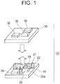
- Fig. 1 is a perspective view showing a structure of a stacked mounting structure by separating into a first substrate 20 and a second substrate 30.
- electronic components 26 are mounted on a principal surface of the first substrate 20.
- electronic components 36 are mounted on the second substrate 30.
- the first substrate 20 and the second substrate 30 are disposed face-to-face.
- a multi-layer substrate or a substrate with built-in electronic components may be used for the first substrate 20 and the second substrate 30.
- Electrodes 22 are provided between the electronic components 26 of the first substrate 20, and electroconductive members 21 having a substantially circular cylindrical shape are installed on the electrodes 22.
- a length of all the electroconductive members 21 is substantially same, and is longer than the maximum height of the electronic component 26 from among the electronic components 26 mounted on the first substrate 20.
- an area of an orthogonal cross-section perpendicular to a longitudinal direction of the electroconductive member 21 is same as or less than an area of the electrodes 22.
- the electroconductive member 21 can be made easily by cutting out from a wire, when a circular cylindrical shaped component is used. At this time, when a diameter of an end portion of a side of the electroconductive portion 21, to be mounted on the first substrate 20 is made substantial, the mounting on the first substrate 20 can be carried out easily and assuredly. Whereas, an end portion of the electroconductive member, on the opposite side of the first substrate 20 can also be mounted in a state of a number of electroconductive members joined.
- the electroconductive member 21 it is preferable to use a material having a lower electrical resistance (such as Cu (copper)). Moreover, it is preferable to apply Au (gold) plating on a surface of the electroconductive member 21 for preventing oxidation of a base material. Furthermore, a surface treatment for making soldering easy is carried out on the electroconductive member 21, and one end portion of the electroconductive member 21, and the electrode 22 are joined to be electroconductive by soldering. Instead of soldering, it is possible to bring into electrical conduction by contact conduction by a method such as an ACP method in which, an anisotropic conductive material is used, an ACF method, and an NCP method.
- a method such as an ACP method in which, an anisotropic conductive material is used, an ACF method, and an NCP method.
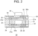
- circuit layers 24 and 34 are formed in the first substrate 20 and the second substrate 30 respectively.
- An insulating layer 23 is formed by filling and curing an insulating material (reinforcing member) of a resin around the electroconductive member 21 and the electronic components 26 on the first substrate 20. In the insulating layer 23, only an end portion 21a of the electroconductive member 21, toward the second substrate 30 is exposed from a surface (an upper surface) 23a toward the second substrate 30.
- Electrodes 32 are installed on a surface 30a of the second substrate 30, facing the first substrate 20, at positions facing the electroconductive members 21.
- the second substrate 30 is joined to a surface of the insulating surface 23 such that the end portions 21a of the electroconductive members 21 of the first substrate 20 and the electrodes 32 are connected electrically.
- the number of stacked layers may be increased further by installing electroconductive members (not shown in the diagram) on electrodes (not shown in the diagram) on the exposed surface of the second substrate 30.
- the electroconductive member connecting the upper and the lower circuit boards can be installed freely between the electronic components, a wiring design of each substrate is not constrained. Furthermore, the electrode on which the electroconductive member is mounted not being a through hole electrode, a land electrode is not necessary, and the electroconductive members can be disposed at a narrow pitch. Therefore, it is possible to provide a stacked mounting structure having a small area of a principal surface of a substrate. Moreover, since processes such as cutting of through holes and recesses in the substrate are not necessary, it is possible to provide a stacked mounting structure at a low price and having a small area of the principal surface of the substrate.
- Fig. 3 is a perspective view showing an other structure of a stacked mounting structure according to the present invention, by separating into a first substrate 50 and a second substrate 60.
- Fig. 4 is an enlarged perspective view showing a relationship of an electroconductive member and a reinforcing member.
- a reinforcing member 57 is formed in a state of a part or whole of a mounting area exposed around an electroconductive member 51.
- the first substrate 20, the electrode 22, the electronic component 26, the second substrate 30, the electronic component 36 in the stacked mounting structure 10 correspond to the first substrate 50, the electroconductive member 51, an electrode 52, an electronic component 56, the second substrate 60, and an electronic component 66 respectively in a stacked mounting structure 40.
- a circuit layer similar to the circuit layers 24 and 34 of the stacked mounting structure 10 is formed.
- the electronic components being exposed after forming the reinforcing member the electronic components can be checked immediately before connecting the second substrate, and the number of defective stacked mounting structures can be reduced.
- the reinforcing member 57 is disposed such that an end portion 51a toward the second substrate 60 is left around the electroconductive member 51.
- a material which is in a liquid form at the time of disposing around the electroconductive member 51, and which is hardened after disposing is to be used.
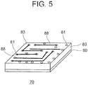
- Fig. 5 is a perspective view showing an other structure of a stacked mounting structure.
- a stacked mounting structure 70 similarly as the insulating layer 23, an insulating layer 83 by an insulating material of a resin is formed around electronic components (not shown in the diagram) and electroconductive members 81 on a first substrate 80, and on a surface of the insulating layer 83, which is far from the first substrate 80, wires 88 are formed to connect the electroconductive members 81.
- the wires 88 are formed directly on the insulating layer 83.
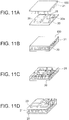
- FIGS. 11A, Fig. 11B, Fig. 11C, and Fig. 11D show stages of a method of manufacturing a stacked mounting structure in accordance with a first embodiment of the invention.
- the end portion of the electroconductive member 21 toward the opposite side of the first substrate 20 can be mounted in the state of the number of electroconductive members 21 joined.
- the state of the number of electroconductive members 21 joined can be formed by forming the electroconductive members 21 by plating of Cu on a substrate 100, or by carrying out press working on a plate 100 of an electroconductive material such as Cu ( Fig. 11A ).
- an electroconductive member 21 which is connected is prepared separately from the first substrate 20, and is connected to the first substrate 20.
- Fig. 11B shows a state of a pin-substrate joining.
- a resin is applied between a portion where the first substrate 20 and the electroconductive members 21 are joined, and cured.
- a resin may be applied in advance on the first substrate 20.
- the portion at which the first substrate 20 and the electroconductive members 21 are joined is removed by grinding, and each electroconductive member 21 is exposed.
- a metal film which prevents oxidation of the electroconductive member 21 is formed at the end portion of the exposed electroconductive members 21.
- the second substrate 30 is stacked as shown in Fig. 11D , and the substrates 20 and 30 are connected. Accordingly, the stacked mounting structure is formed. Therefore, in a case in which the height of the electronic component 26 is comparatively high such as from 0.3 mm to 1 mm, by disposing freely the electroconductive members 21 longer than the height of the electronic component 26 on a principal surface 20a of the first substrate 20, it is possible to connect the first substrate 20 and the second substrate 30. Moreover, it is possible to narrow a pitch of connections.
- the electroconductive members 21 are mounted collectively on the first substrate 20 in the state of the plurality of one end portions joined. Therefore, it is possible to mount the electroconductive members 21 easily. Moreover, since protruding electrodes can be prepared collectively, further narrowing of pitch is possible. As a result, the stacked mounting structure can be easily manufactured to be small.
- Fig. 6 is a flowchart showing a flow of a method of manufacturing stacked mounting structure.
- the electronic components 26 are mounted on the first substrate 20 (step S1), and at the same time, the electroconductive members 21 are mounted on the electrodes 22 of the first substrate 20 (step S2).
- a prevalent surface mounting process may be used.
- the electroconductive members 21 can be mounted by a method in which, a cream solder and flux are supplied on the electrodes 22 by a method such as printing, and the electroconductive members are positioned and fixed on the electrodes 22 by using a mounting instrument and jig, and heated.
- the electroconductive members 21 may be mounted after the electronic components 26 are mounted (refer to the fifth embodiment or the sixth embodiment), or vice versa.
- the insulating layer 23 is formed around the electronic components 26 and the electroconductive members 21 on the first substrate 20 by applying a liquid sealing resin on the first substrate 20 on which the electronic components 26 and the electroconductive members 21 are mounted such that, the end surface 21a on the opposite side of the first substrate 20 (toward the second substrate 30) is exposed, and then curing the liquid sealing resin. Accordingly, the electroconductive members 21 and the electronic components 26 are sealed (step S3).
- a curing method of resin methods such as a thermal curing and two-liquid mixing are available.
- the shape of the resin after curing can be set easily by using a mould which is matched with an outer shape of the first substrate 20 or a desired shape after curing.
- a reinforcing member can be disposed around the electroconductive members.
- the second substrate 30 is connected by stacking on the first substrate 20 via the bump in the form of a metal film formed on an end surface of the electroconductive member 21, on the opposite side of the first substrate 20. Without stacking the second substrate 30, wires can be formed directly on a surface 23a of the insulating layer 23, on the opposite side of the first substrate 20.
- the stacked mounting structure being manufactured by the abovementioned steps, it is possible to provide the stacked mounting structure having a small area of a principal surface of the substrate by extremely less number of steps.
- Fig. 7 is a flowchart showing a flow of an other method of manufacturing stacked mounting structure. Steps of mounting electronic components (step S1), mounting electroconductive members (step S2), and resin sealing (step S3) being same as above and the description of these steps is omitted.
- the upper surface 23a of the insulating layer 23 is ground and flattened to be parallel to the principal surface 20a of the first substrate 20, as well as, each of the end surfaces 21a of the electroconductive members 21, on the opposite side of the first substrate 20 is exposed (step S4).
- a metal film (UBM layer) is formed on the end surface 21a of the exposed electroconductive member 21 (step S5).
- UBM layer a metal film
- the bump is formed on the metal film which is formed on the end surface 21a of the exposed electroconductive member 21 (step S6).
- Solder or gold can be used as a material of bump.
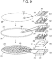
- the second substrate 30 is connected by stacking via a bump 29 ( Fig. 9 and Fig. 10 ) on the metal film which is formed on the end surface 21a of the electroconductive member 21.
- the end surface 21a of the electroconductive member 21 has a structure which makes it easy to connect the second substrate 30. Consequently, it is possible to provide a stacked mounting structure having a high quality of connection of the first substrate 20 and the second substrate 30, and small area of the principal surface of the substrate.
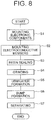
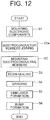
- Fig. 8 is a flowchart showing a flow of an other method of manufacturing stacked mounting structure.
- Fig. 9 is a diagram of which, a right side is an enlarged perspective view showing a structure of a stacked mounting structure corresponding to steps from Step S1 to step S6 in Fig. 8 , and left side is a perspective view showing an assembled state of the stacked mounting structure separated into pieces in the right-side diagram.
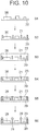
- Fig. 10 is a side view showing a structure of the stacked mounting structure corresponding to steps from step S1 to step S6 in Fig. 8 .
- Steps of mounting electronic components are same as above.
- step S1 mounting electroconductive members
- step S3 resin sealing
- step S4 grinding
- step S5 UBM layer formation
- step S6 bump formation
- step S7 After forming the bump 29, a plurality of modules 90 is formed on the first substrate 20, and by a step of separating such as dicing, the modules are turned to be individual modules (step S7).
- Fig. 12 is a flow chart showing a flow of a further method of manufacturing stacked mounting structure. Same reference numerals are assigned to contents which are same as described above, and repeated description of such steps is omitted.
- the electronic components 26 are mounted on the first substrate 20 (step S1).
- step S2a a state in which one end portions of some of the electroconductive members 21 are connected is formed.
- various methods such as forming Cu by plating on the substrate 10, furthermore, forming the electroconductive members 21 by a method such as press working on a plate 100 of an electroconductive material such as Cu, and plating the end surfaces in a state of the rod-shaped electroconductive members 21 arranged to be aligned on a jig, can be used.
- the electroconductive members 21 are formed such that the height of the electroconductive member 21 is more than the height of the electronic component 26.
- step S2 The end portion of the electroconductive member 21, on the side which is not connected, is joined to the electrode of the principal surface 20a of the first substrate 20 (step S2).
- step S2 In a state of the one end portion of the electroconductive member 21 joined, when Au plating is applied on a surface thereof, oxidation of Cu is prevented and the soldering can be carried out assuredly.
- a resin is applied between portions at which, the first substrate 20 and the electroconductive members 21 are joined, and cured (step S3).
- the resin may be applied in advance on the first substrate 20.
- a portion at which the first substrate 20 and the electroconductive members 21 are joined is removed by grinding, and each electroconductive member 21 is exposed (step S4).
- Surrounding of the electroconductive member 21 is reinforced by resin. Therefore, the electroconductive member 21 can be ground stably. Furthermore, the height (length) of the electroconductive members 21 can be arranged precisely by grinding. Therefore, a tolerance of length of the electroconductive member 21 to be used can be widened.
- the electroconductive member 21 longer than the height of the electronic components 26 can be disposed freely on the principal surface 20a of the first substrate 20, and the first substrate 20 and the second substrate 30 can be joined. Moreover, pitch of connections can be narrowed.
- the electroconductive members 21 are mounted on the first substrate 20 in the state of the plurality of one end portions joined. Therefore, the electroconductive members 21 can be mounted easily. Moreover, since protruding electrodes can be prepared collectively, further narrowing is possible. As a result, the stacked mounting structure can be easily manufactured to be small.
- the electroconductive members which connect the upper and the lower circuit boards can be disposed freely between the electronic components, wiring design of each substrate is not constrained. Furthermore, the electrodes on which the electroconductive members are mounted not being through-hole electrode, land electrodes are not required, and the electroconductive members can be disposed with a narrow pitch. Therefore, it is possible to provide a stacked mounting structure having a small area of the principal surface of the substrate.
- the method of manufacturing a stacked mounting structure according to the present invention is useful for small sizing of a mounting structure main body, and particularly, appropriate for highly dense mounting of an image picking unit at a front end of an endoscope.
Claims (2)
- Verfahren zur Herstellung einer gestapelten Montagestruktur, wobei die gestapelte Montagestruktur aus mindestens zwei aufeinander gestapelten Substraten (20, 30) besteht; mit folgenden Schritten:a) Montage elektronischer Bauteile (26) auf einer Hauptoberfläche (20a) eines der Substrate (20, 30);b) Montage elektronischer Bauteile (26) auf einer Oberfläche des anderen (30) Substrates, wobei die Oberfläche des anderen Substrates (30) sich gegenüber einer Hauptoberfläche (30a) des anderen Substrates (30) befindet, welche in der fertigen gestapelten Montagestruktur der Hauptoberfläche (20a) des einen Substrates (20) zugewandt sein wird;c) Bildung einer Vielzahl von elektrisch leitenden Elementen (21) auf einer Platte (100) aus einem elektrisch leitenden Material in verbundener Weise, wobei die elektrisch leitenden Elemente (21) höher sind als die Höhe der Bauteile (26) auf der Hauptoberfläche (20a) des einen Substrates (20);d) Platzieren der Platte (100) über der Hauptoberfläche (20a) des einen Substrates (20), um die Vielzahl von elektrisch leitenden Elementen (21) mit der Hauptoberfläche (20a) des einen Substrates (20) zu kontaktieren und zu verbinden;e) Entfernen der Platte (100) durch Abschleifen, um die Enden der elektrisch leitenden Elemente (21) freizulegen; undf) Stapeln des anderen Substrates (30) auf dem einen Substrat (20), wobei die Hauptoberfläche (30a) des anderen Substrates (30) den Enden der elektrisch leitenden Elemente (21) zugewandt ist und somit die Substrate verbindet,wobei außerdem ein Harz zwischen dem einen Substrat (20) und der Platte (100) entweder vor oder nach dem Schritt d) aufgebracht wird, das Harz wird vor dem Schritt e) gehärtet; und
nach dem Entfernen der Platte (100) in Schritt e) wird zum Verhindern von Oxidation ein Metallfilm auf den Enden der elektrisch leitenden Elemente (21) aufgebracht, welche in Schritt e) freigelegt wurden. - Verfahren nach Anspruch 1, wobei die elektrisch leitenden Elemente (21) stabförmig ausgebildet sind.
Applications Claiming Priority (3)
| Application Number | Priority Date | Filing Date | Title |
|---|---|---|---|
| JP2007240785 | 2007-09-18 | ||
| JP2008091636A JP2009094457A (ja) | 2007-09-18 | 2008-03-31 | 積層実装構造体及び積層実装構造体の製造方法 |
| PCT/JP2008/066655 WO2009038042A1 (ja) | 2007-09-18 | 2008-09-16 | 積層実装構造体及び積層実装構造体の製造方法 |
Publications (3)
| Publication Number | Publication Date |
|---|---|
| EP2194576A1 EP2194576A1 (de) | 2010-06-09 |
| EP2194576A4 EP2194576A4 (de) | 2010-10-06 |
| EP2194576B1 true EP2194576B1 (de) | 2017-12-06 |
Family
ID=40467856
Family Applications (1)
| Application Number | Title | Priority Date | Filing Date |
|---|---|---|---|
| EP08832607.9A Not-in-force EP2194576B1 (de) | 2007-09-18 | 2008-09-16 | Verfahren zur herstellung einer gestapelten montagestruktur |
Country Status (5)
| Country | Link |
|---|---|
| US (2) | US20100202126A1 (de) |
| EP (1) | EP2194576B1 (de) |
| JP (1) | JP2009094457A (de) |
| CN (1) | CN101803020B (de) |
| WO (1) | WO2009038042A1 (de) |
Families Citing this family (19)
| Publication number | Priority date | Publication date | Assignee | Title |
|---|---|---|---|---|
| JP5449237B2 (ja) * | 2011-03-09 | 2014-03-19 | 古河電気工業株式会社 | 基板および基板の製造方法 |
| JP2014123638A (ja) * | 2012-12-21 | 2014-07-03 | Murata Mfg Co Ltd | 部品モジュール |
| JP6205228B2 (ja) * | 2013-09-30 | 2017-09-27 | オリンパス株式会社 | 撮像モジュールおよび内視鏡装置 |
| DE102014101366B3 (de) * | 2014-02-04 | 2015-05-13 | Infineon Technologies Ag | Chip-Montage an über Chip hinausstehender Adhäsions- bzw. Dielektrikumsschicht auf Substrat |
| KR20150092881A (ko) * | 2014-02-06 | 2015-08-17 | 엘지이노텍 주식회사 | 인쇄회로기판, 패키지 기판 및 이의 제조 방법 |
| JP6274135B2 (ja) * | 2015-03-12 | 2018-02-07 | 株式会社村田製作所 | コイルモジュール |
| EP3324416A4 (de) * | 2015-07-15 | 2019-02-20 | Murata Manufacturing Co., Ltd. | Elektronische komponente |
| US10297576B2 (en) | 2016-04-18 | 2019-05-21 | Skyworks Solutions, Inc. | Reduced form factor radio frequency system-in-package |
| US10062670B2 (en) | 2016-04-18 | 2018-08-28 | Skyworks Solutions, Inc. | Radio frequency system-in-package with stacked clocking crystal |
| US10269769B2 (en) | 2016-04-18 | 2019-04-23 | Skyworks Solutions, Inc. | System in package with vertically arranged radio frequency componentry |
| US9918386B2 (en) | 2016-04-18 | 2018-03-13 | Skyworks Solutions, Inc. | Surface mount device stacking for reduced form factor |
| TW202329611A (zh) | 2016-12-29 | 2023-07-16 | 美商天工方案公司 | 前端系統及相關裝置、積體電路、模組及方法 |
| US10515924B2 (en) | 2017-03-10 | 2019-12-24 | Skyworks Solutions, Inc. | Radio frequency modules |
| DE102017212739A1 (de) | 2017-07-25 | 2019-01-31 | Siemens Aktiengesellschaft | Halbleiterbauteil sowie Verfahren zu dessen Herstellung |
| CN109714910B (zh) * | 2019-01-29 | 2020-08-14 | 维沃移动通信有限公司 | 一种多层电路板的制造方法、多层电路板和移动终端 |
| JP2022080657A (ja) * | 2020-11-18 | 2022-05-30 | 株式会社ディスコ | ウェーハの製造方法及び積層デバイスチップの製造方法 |
| JP2022080653A (ja) * | 2020-11-18 | 2022-05-30 | 株式会社ディスコ | ウェーハの製造方法及び積層デバイスチップの製造方法 |
| JP2022080658A (ja) * | 2020-11-18 | 2022-05-30 | 株式会社ディスコ | ウェーハの製造方法及び積層デバイスチップの製造方法 |
| JP2022080655A (ja) * | 2020-11-18 | 2022-05-30 | 株式会社ディスコ | ウェーハの製造方法及び積層デバイスチップの製造方法 |
Citations (4)
| Publication number | Priority date | Publication date | Assignee | Title |
|---|---|---|---|---|
| JP2000323806A (ja) * | 1999-05-13 | 2000-11-24 | Matsushita Electric Ind Co Ltd | バンプ付セラミック回路基板及びその製造方法 |
| US6222259B1 (en) * | 1998-09-15 | 2001-04-24 | Hyundai Electronics Industries Co., Ltd. | Stack package and method of fabricating the same |
| JP2002134653A (ja) * | 2000-10-23 | 2002-05-10 | Matsushita Electric Ind Co Ltd | 半導体装置とその製造方法 |
| US20060284309A1 (en) * | 2005-06-16 | 2006-12-21 | Samsung Electronics Co., Ltd. | Integrated circuit package and integrated circuit module |
Family Cites Families (13)
| Publication number | Priority date | Publication date | Assignee | Title |
|---|---|---|---|---|
| JPH05102149A (ja) * | 1991-10-04 | 1993-04-23 | Sharp Corp | 半導体装置の製造方法 |
| US5334804A (en) * | 1992-11-17 | 1994-08-02 | Fujitsu Limited | Wire interconnect structures for connecting an integrated circuit to a substrate |
| US5977640A (en) * | 1998-06-26 | 1999-11-02 | International Business Machines Corporation | Highly integrated chip-on-chip packaging |
| JP3833859B2 (ja) * | 1999-10-14 | 2006-10-18 | ローム株式会社 | 半導体装置およびその製造方法 |
| EP1154474A4 (de) * | 1999-08-23 | 2008-07-16 | Rohm Co Ltd | Halbleiter-bauteil und verfahren zur herstellung hierfür |
| US6448106B1 (en) | 1999-11-09 | 2002-09-10 | Fujitsu Limited | Modules with pins and methods for making modules with pins |
| JP2001144399A (ja) | 1999-11-17 | 2001-05-25 | Sony Corp | 基板間接続部材、電子回路基板、電子回路装置及び電子回路装置の製造方法 |
| JP4320492B2 (ja) * | 1999-12-08 | 2009-08-26 | 株式会社デンソー | 半導体素子の実装構造および半導体素子の実装構造の製造方法 |
| JP4380088B2 (ja) * | 2001-05-31 | 2009-12-09 | 株式会社デンソー | 積層回路モジュールの製造方法 |
| JP2006165252A (ja) | 2004-12-07 | 2006-06-22 | Shinko Electric Ind Co Ltd | チップ内蔵基板の製造方法 |
| JP4635202B2 (ja) * | 2005-07-20 | 2011-02-23 | 国立大学法人九州工業大学 | 両面電極パッケージの製造方法 |
| JP3960479B1 (ja) * | 2006-07-07 | 2007-08-15 | 国立大学法人九州工業大学 | 両面電極構造の半導体装置の製造方法 |
| JP4793155B2 (ja) * | 2006-07-31 | 2011-10-12 | エプソントヨコム株式会社 | プリント基板、プリント基板ユニット、表面実装型高安定圧電発振器、及びプリント基板の加工方法 |
-
2008
- 2008-03-31 JP JP2008091636A patent/JP2009094457A/ja active Pending
- 2008-09-16 CN CN2008801075629A patent/CN101803020B/zh active Active
- 2008-09-16 EP EP08832607.9A patent/EP2194576B1/de not_active Not-in-force
- 2008-09-16 WO PCT/JP2008/066655 patent/WO2009038042A1/ja active Application Filing
- 2008-09-16 US US12/678,855 patent/US20100202126A1/en not_active Abandoned
-
2012
- 2012-11-05 US US13/668,982 patent/US10244639B2/en active Active
Patent Citations (4)
| Publication number | Priority date | Publication date | Assignee | Title |
|---|---|---|---|---|
| US6222259B1 (en) * | 1998-09-15 | 2001-04-24 | Hyundai Electronics Industries Co., Ltd. | Stack package and method of fabricating the same |
| JP2000323806A (ja) * | 1999-05-13 | 2000-11-24 | Matsushita Electric Ind Co Ltd | バンプ付セラミック回路基板及びその製造方法 |
| JP2002134653A (ja) * | 2000-10-23 | 2002-05-10 | Matsushita Electric Ind Co Ltd | 半導体装置とその製造方法 |
| US20060284309A1 (en) * | 2005-06-16 | 2006-12-21 | Samsung Electronics Co., Ltd. | Integrated circuit package and integrated circuit module |
Also Published As
| Publication number | Publication date |
|---|---|
| JP2009094457A (ja) | 2009-04-30 |
| US10244639B2 (en) | 2019-03-26 |
| EP2194576A4 (de) | 2010-10-06 |
| WO2009038042A1 (ja) | 2009-03-26 |
| US20100202126A1 (en) | 2010-08-12 |
| US20130133190A1 (en) | 2013-05-30 |
| CN101803020B (zh) | 2012-05-23 |
| EP2194576A1 (de) | 2010-06-09 |
| CN101803020A (zh) | 2010-08-11 |
Similar Documents
| Publication | Publication Date | Title |
|---|---|---|
| EP2194576B1 (de) | Verfahren zur herstellung einer gestapelten montagestruktur | |
| CN101843181B (zh) | 内置元件电路板 | |
| US7076869B2 (en) | Solid via layer to layer interconnect | |
| US20120080221A1 (en) | Printed wiring board with built-in component and its manufacturing method | |
| JPH07240496A (ja) | 半導体装置、その製造方法、半導体素子のテスト方法、そのテスト基板およびそのテスト基板の製造方法 | |
| EP2750490A1 (de) | Bestückungsleiterplatte und herstellungsverfahren dafür | |
| KR101608745B1 (ko) | 인쇄회로기판조립체의 제조방법 | |
| JP2001332866A (ja) | 回路基板及びその製造方法 | |
| KR101586633B1 (ko) | 플렉스 회로와 기밀하게 패킹된 어레이의 상호 접속 | |
| JP2009252942A (ja) | 部品内蔵配線板、部品内蔵配線板の製造方法 | |
| WO2007040193A1 (ja) | ハイブリッド集積回路装置とその製造方法 | |
| WO2010067508A1 (ja) | 多層基板およびその製造方法 | |
| US10448510B2 (en) | Multilayer substrate and electronic device | |
| US20190254164A1 (en) | Circuit board, method of manufacturing circuit board, and electronic device | |
| US9929116B2 (en) | Electronic device module and method of manufacturing the same | |
| JP5397012B2 (ja) | 部品内蔵配線板、部品内蔵配線板の製造方法 | |
| US20170294258A1 (en) | Built-in-coil substrate and method for manufacturing the same | |
| US8546186B2 (en) | Planar interconnect structure for hybrid circuits | |
| JP3930222B2 (ja) | 半導体装置の製造方法 | |
| JP2011151103A (ja) | 電子部品相互の接続構造及び接続方法 | |
| US20100155928A1 (en) | Semiconductor package and manufacturing method of the same | |
| JP5654109B2 (ja) | 積層実装構造体の製造方法 | |
| CN108305864B (zh) | 端子 | |
| KR101184784B1 (ko) | 전자부품 내장기판 제조방법 및 전자부품 내장기판 | |
| JP4954778B2 (ja) | 三次元電子回路装置および連結部材 |
Legal Events
| Date | Code | Title | Description |
|---|---|---|---|
| PUAI | Public reference made under article 153(3) epc to a published international application that has entered the european phase |
Free format text: ORIGINAL CODE: 0009012 |
|
| 17P | Request for examination filed |
Effective date: 20100322 |
|
| AK | Designated contracting states |
Kind code of ref document: A1 Designated state(s): AT BE BG CH CY CZ DE DK EE ES FI FR GB GR HR HU IE IS IT LI LT LU LV MC MT NL NO PL PT RO SE SI SK TR |
|
| AX | Request for extension of the european patent |
Extension state: AL BA MK RS |
|
| A4 | Supplementary search report drawn up and despatched |
Effective date: 20100903 |
|
| DAX | Request for extension of the european patent (deleted) | ||
| 17Q | First examination report despatched |
Effective date: 20140307 |
|
| RAP1 | Party data changed (applicant data changed or rights of an application transferred) |
Owner name: OLYMPUS CORPORATION |
|
| REG | Reference to a national code |
Ref country code: DE Ref legal event code: R079 Ref document number: 602008053267 Country of ref document: DE Free format text: PREVIOUS MAIN CLASS: H01L0025065000 Ipc: H01L0025070000 |
|
| GRAP | Despatch of communication of intention to grant a patent |
Free format text: ORIGINAL CODE: EPIDOSNIGR1 |
|
| RIC1 | Information provided on ipc code assigned before grant |
Ipc: H01L 23/31 20060101ALN20170516BHEP Ipc: H01L 25/10 20060101ALI20170516BHEP Ipc: H01L 25/065 20060101ALI20170516BHEP Ipc: H05K 3/34 20060101ALN20170516BHEP Ipc: H01L 25/07 20060101AFI20170516BHEP Ipc: H05K 3/30 20060101ALI20170516BHEP Ipc: H05K 1/14 20060101ALI20170516BHEP Ipc: H05K 3/28 20060101ALN20170516BHEP Ipc: H05K 3/36 20060101ALN20170516BHEP |
|
| RIC1 | Information provided on ipc code assigned before grant |
Ipc: H01L 25/10 20060101ALI20170530BHEP Ipc: H01L 25/07 20060101AFI20170530BHEP Ipc: H05K 3/30 20060101ALI20170530BHEP Ipc: H05K 3/28 20060101ALN20170530BHEP Ipc: H05K 3/36 20060101ALN20170530BHEP Ipc: H05K 3/34 20060101ALN20170530BHEP Ipc: H01L 25/065 20060101ALI20170530BHEP Ipc: H05K 1/14 20060101ALI20170530BHEP Ipc: H01L 23/31 20060101ALN20170530BHEP |
|
| INTG | Intention to grant announced |
Effective date: 20170614 |
|
| RIN1 | Information on inventor provided before grant (corrected) |
Inventor name: NAKAMURA, MIKIO Inventor name: KONDO, YU |
|
| GRAS | Grant fee paid |
Free format text: ORIGINAL CODE: EPIDOSNIGR3 |
|
| GRAA | (expected) grant |
Free format text: ORIGINAL CODE: 0009210 |
|
| AK | Designated contracting states |
Kind code of ref document: B1 Designated state(s): AT BE BG CH CY CZ DE DK EE ES FI FR GB GR HR HU IE IS IT LI LT LU LV MC MT NL NO PL PT RO SE SI SK TR |
|
| REG | Reference to a national code |
Ref country code: GB Ref legal event code: FG4D |
|
| REG | Reference to a national code |
Ref country code: AT Ref legal event code: REF Ref document number: 953108 Country of ref document: AT Kind code of ref document: T Effective date: 20171215 Ref country code: CH Ref legal event code: EP |
|
| REG | Reference to a national code |
Ref country code: IE Ref legal event code: FG4D |
|
| REG | Reference to a national code |
Ref country code: DE Ref legal event code: R096 Ref document number: 602008053267 Country of ref document: DE |
|
| REG | Reference to a national code |
Ref country code: NL Ref legal event code: MP Effective date: 20171206 |
|
| REG | Reference to a national code |
Ref country code: LT Ref legal event code: MG4D |
|
| PG25 | Lapsed in a contracting state [announced via postgrant information from national office to epo] |
Ref country code: NO Free format text: LAPSE BECAUSE OF FAILURE TO SUBMIT A TRANSLATION OF THE DESCRIPTION OR TO PAY THE FEE WITHIN THE PRESCRIBED TIME-LIMIT Effective date: 20180306 Ref country code: SE Free format text: LAPSE BECAUSE OF FAILURE TO SUBMIT A TRANSLATION OF THE DESCRIPTION OR TO PAY THE FEE WITHIN THE PRESCRIBED TIME-LIMIT Effective date: 20171206 Ref country code: FI Free format text: LAPSE BECAUSE OF FAILURE TO SUBMIT A TRANSLATION OF THE DESCRIPTION OR TO PAY THE FEE WITHIN THE PRESCRIBED TIME-LIMIT Effective date: 20171206 Ref country code: ES Free format text: LAPSE BECAUSE OF FAILURE TO SUBMIT A TRANSLATION OF THE DESCRIPTION OR TO PAY THE FEE WITHIN THE PRESCRIBED TIME-LIMIT Effective date: 20171206 Ref country code: LT Free format text: LAPSE BECAUSE OF FAILURE TO SUBMIT A TRANSLATION OF THE DESCRIPTION OR TO PAY THE FEE WITHIN THE PRESCRIBED TIME-LIMIT Effective date: 20171206 |
|
| REG | Reference to a national code |
Ref country code: AT Ref legal event code: MK05 Ref document number: 953108 Country of ref document: AT Kind code of ref document: T Effective date: 20171206 |
|
| PG25 | Lapsed in a contracting state [announced via postgrant information from national office to epo] |
Ref country code: HR Free format text: LAPSE BECAUSE OF FAILURE TO SUBMIT A TRANSLATION OF THE DESCRIPTION OR TO PAY THE FEE WITHIN THE PRESCRIBED TIME-LIMIT Effective date: 20171206 Ref country code: LV Free format text: LAPSE BECAUSE OF FAILURE TO SUBMIT A TRANSLATION OF THE DESCRIPTION OR TO PAY THE FEE WITHIN THE PRESCRIBED TIME-LIMIT Effective date: 20171206 Ref country code: GR Free format text: LAPSE BECAUSE OF FAILURE TO SUBMIT A TRANSLATION OF THE DESCRIPTION OR TO PAY THE FEE WITHIN THE PRESCRIBED TIME-LIMIT Effective date: 20180307 Ref country code: BG Free format text: LAPSE BECAUSE OF FAILURE TO SUBMIT A TRANSLATION OF THE DESCRIPTION OR TO PAY THE FEE WITHIN THE PRESCRIBED TIME-LIMIT Effective date: 20180306 |
|
| PG25 | Lapsed in a contracting state [announced via postgrant information from national office to epo] |
Ref country code: NL Free format text: LAPSE BECAUSE OF FAILURE TO SUBMIT A TRANSLATION OF THE DESCRIPTION OR TO PAY THE FEE WITHIN THE PRESCRIBED TIME-LIMIT Effective date: 20171206 |
|
| PG25 | Lapsed in a contracting state [announced via postgrant information from national office to epo] |
Ref country code: CZ Free format text: LAPSE BECAUSE OF FAILURE TO SUBMIT A TRANSLATION OF THE DESCRIPTION OR TO PAY THE FEE WITHIN THE PRESCRIBED TIME-LIMIT Effective date: 20171206 Ref country code: EE Free format text: LAPSE BECAUSE OF FAILURE TO SUBMIT A TRANSLATION OF THE DESCRIPTION OR TO PAY THE FEE WITHIN THE PRESCRIBED TIME-LIMIT Effective date: 20171206 Ref country code: SK Free format text: LAPSE BECAUSE OF FAILURE TO SUBMIT A TRANSLATION OF THE DESCRIPTION OR TO PAY THE FEE WITHIN THE PRESCRIBED TIME-LIMIT Effective date: 20171206 |
|
| PG25 | Lapsed in a contracting state [announced via postgrant information from national office to epo] |
Ref country code: RO Free format text: LAPSE BECAUSE OF FAILURE TO SUBMIT A TRANSLATION OF THE DESCRIPTION OR TO PAY THE FEE WITHIN THE PRESCRIBED TIME-LIMIT Effective date: 20171206 Ref country code: PL Free format text: LAPSE BECAUSE OF FAILURE TO SUBMIT A TRANSLATION OF THE DESCRIPTION OR TO PAY THE FEE WITHIN THE PRESCRIBED TIME-LIMIT Effective date: 20171206 Ref country code: AT Free format text: LAPSE BECAUSE OF FAILURE TO SUBMIT A TRANSLATION OF THE DESCRIPTION OR TO PAY THE FEE WITHIN THE PRESCRIBED TIME-LIMIT Effective date: 20171206 Ref country code: IT Free format text: LAPSE BECAUSE OF FAILURE TO SUBMIT A TRANSLATION OF THE DESCRIPTION OR TO PAY THE FEE WITHIN THE PRESCRIBED TIME-LIMIT Effective date: 20171206 |
|
| REG | Reference to a national code |
Ref country code: DE Ref legal event code: R097 Ref document number: 602008053267 Country of ref document: DE |
|
| PLBE | No opposition filed within time limit |
Free format text: ORIGINAL CODE: 0009261 |
|
| STAA | Information on the status of an ep patent application or granted ep patent |
Free format text: STATUS: NO OPPOSITION FILED WITHIN TIME LIMIT |
|
| PGFP | Annual fee paid to national office [announced via postgrant information from national office to epo] |
Ref country code: DE Payment date: 20180905 Year of fee payment: 11 |
|
| 26N | No opposition filed |
Effective date: 20180907 |
|
| PG25 | Lapsed in a contracting state [announced via postgrant information from national office to epo] |
Ref country code: DK Free format text: LAPSE BECAUSE OF FAILURE TO SUBMIT A TRANSLATION OF THE DESCRIPTION OR TO PAY THE FEE WITHIN THE PRESCRIBED TIME-LIMIT Effective date: 20171206 Ref country code: SI Free format text: LAPSE BECAUSE OF FAILURE TO SUBMIT A TRANSLATION OF THE DESCRIPTION OR TO PAY THE FEE WITHIN THE PRESCRIBED TIME-LIMIT Effective date: 20171206 |
|
| PG25 | Lapsed in a contracting state [announced via postgrant information from national office to epo] |
Ref country code: MC Free format text: LAPSE BECAUSE OF FAILURE TO SUBMIT A TRANSLATION OF THE DESCRIPTION OR TO PAY THE FEE WITHIN THE PRESCRIBED TIME-LIMIT Effective date: 20171206 |
|
| REG | Reference to a national code |
Ref country code: CH Ref legal event code: PL |
|
| GBPC | Gb: european patent ceased through non-payment of renewal fee |
Effective date: 20180916 |
|
| REG | Reference to a national code |
Ref country code: BE Ref legal event code: MM Effective date: 20180930 |
|
| REG | Reference to a national code |
Ref country code: IE Ref legal event code: MM4A |
|
| PG25 | Lapsed in a contracting state [announced via postgrant information from national office to epo] |
Ref country code: LU Free format text: LAPSE BECAUSE OF NON-PAYMENT OF DUE FEES Effective date: 20180916 |
|
| PG25 | Lapsed in a contracting state [announced via postgrant information from national office to epo] |
Ref country code: IE Free format text: LAPSE BECAUSE OF NON-PAYMENT OF DUE FEES Effective date: 20180916 |
|
| PG25 | Lapsed in a contracting state [announced via postgrant information from national office to epo] |
Ref country code: CH Free format text: LAPSE BECAUSE OF NON-PAYMENT OF DUE FEES Effective date: 20180930 Ref country code: BE Free format text: LAPSE BECAUSE OF NON-PAYMENT OF DUE FEES Effective date: 20180930 Ref country code: LI Free format text: LAPSE BECAUSE OF NON-PAYMENT OF DUE FEES Effective date: 20180930 Ref country code: FR Free format text: LAPSE BECAUSE OF NON-PAYMENT OF DUE FEES Effective date: 20180930 |
|
| PG25 | Lapsed in a contracting state [announced via postgrant information from national office to epo] |
Ref country code: GB Free format text: LAPSE BECAUSE OF NON-PAYMENT OF DUE FEES Effective date: 20180916 |
|
| PG25 | Lapsed in a contracting state [announced via postgrant information from national office to epo] |
Ref country code: MT Free format text: LAPSE BECAUSE OF NON-PAYMENT OF DUE FEES Effective date: 20180916 |
|
| PG25 | Lapsed in a contracting state [announced via postgrant information from national office to epo] |
Ref country code: TR Free format text: LAPSE BECAUSE OF FAILURE TO SUBMIT A TRANSLATION OF THE DESCRIPTION OR TO PAY THE FEE WITHIN THE PRESCRIBED TIME-LIMIT Effective date: 20171206 |
|
| REG | Reference to a national code |
Ref country code: DE Ref legal event code: R119 Ref document number: 602008053267 Country of ref document: DE |
|
| PG25 | Lapsed in a contracting state [announced via postgrant information from national office to epo] |
Ref country code: HU Free format text: LAPSE BECAUSE OF FAILURE TO SUBMIT A TRANSLATION OF THE DESCRIPTION OR TO PAY THE FEE WITHIN THE PRESCRIBED TIME-LIMIT; INVALID AB INITIO Effective date: 20080916 Ref country code: PT Free format text: LAPSE BECAUSE OF FAILURE TO SUBMIT A TRANSLATION OF THE DESCRIPTION OR TO PAY THE FEE WITHIN THE PRESCRIBED TIME-LIMIT Effective date: 20171206 |
|
| PG25 | Lapsed in a contracting state [announced via postgrant information from national office to epo] |
Ref country code: CY Free format text: LAPSE BECAUSE OF FAILURE TO SUBMIT A TRANSLATION OF THE DESCRIPTION OR TO PAY THE FEE WITHIN THE PRESCRIBED TIME-LIMIT Effective date: 20171206 |
|
| PG25 | Lapsed in a contracting state [announced via postgrant information from national office to epo] |
Ref country code: DE Free format text: LAPSE BECAUSE OF NON-PAYMENT OF DUE FEES Effective date: 20200401 Ref country code: IS Free format text: LAPSE BECAUSE OF FAILURE TO SUBMIT A TRANSLATION OF THE DESCRIPTION OR TO PAY THE FEE WITHIN THE PRESCRIBED TIME-LIMIT Effective date: 20180406 |