EP2192653A2 - Dispositif d'antenne, équipement de communication radio, antenne assemblée à la surface, carte de circuit imprimé, et procédé de fabrication d'antenne assemblée en surface et la carte de circuit imprimé - Google Patents
Dispositif d'antenne, équipement de communication radio, antenne assemblée à la surface, carte de circuit imprimé, et procédé de fabrication d'antenne assemblée en surface et la carte de circuit imprimé Download PDFInfo
- Publication number
- EP2192653A2 EP2192653A2 EP09014708A EP09014708A EP2192653A2 EP 2192653 A2 EP2192653 A2 EP 2192653A2 EP 09014708 A EP09014708 A EP 09014708A EP 09014708 A EP09014708 A EP 09014708A EP 2192653 A2 EP2192653 A2 EP 2192653A2
- Authority
- EP
- European Patent Office
- Prior art keywords
- antenna
- power supply
- pattern
- supply line
- conductor patterns
- Prior art date
- Legal status (The legal status is an assumption and is not a legal conclusion. Google has not performed a legal analysis and makes no representation as to the accuracy of the status listed.)
- Withdrawn
Links
- 238000004891 communication Methods 0.000 title claims description 17
- 238000004519 manufacturing process Methods 0.000 title claims description 10
- 239000004020 conductor Substances 0.000 claims abstract description 204
- 239000000758 substrate Substances 0.000 claims abstract description 53
- 230000001939 inductive effect Effects 0.000 description 13
- 239000000463 material Substances 0.000 description 10
- 230000005855 radiation Effects 0.000 description 6
- 239000000919 ceramic Substances 0.000 description 5
- 239000003989 dielectric material Substances 0.000 description 5
- RYGMFSIKBFXOCR-UHFFFAOYSA-N Copper Chemical compound [Cu] RYGMFSIKBFXOCR-UHFFFAOYSA-N 0.000 description 4
- 238000010586 diagram Methods 0.000 description 4
- 229910000679 solder Inorganic materials 0.000 description 4
- 239000011889 copper foil Substances 0.000 description 3
- VYPSYNLAJGMNEJ-UHFFFAOYSA-N Silicium dioxide Chemical compound O=[Si]=O VYPSYNLAJGMNEJ-UHFFFAOYSA-N 0.000 description 2
- GWEVSGVZZGPLCZ-UHFFFAOYSA-N Titan oxide Chemical compound O=[Ti]=O GWEVSGVZZGPLCZ-UHFFFAOYSA-N 0.000 description 2
- 239000003990 capacitor Substances 0.000 description 2
- 230000001413 cellular effect Effects 0.000 description 2
- 238000005520 cutting process Methods 0.000 description 2
- 230000000694 effects Effects 0.000 description 2
- 238000005530 etching Methods 0.000 description 2
- 238000007650 screen-printing Methods 0.000 description 2
- BQCADISMDOOEFD-UHFFFAOYSA-N Silver Chemical compound [Ag] BQCADISMDOOEFD-UHFFFAOYSA-N 0.000 description 1
- IHWJXGQYRBHUIF-UHFFFAOYSA-N [Ag].[Pt] Chemical compound [Ag].[Pt] IHWJXGQYRBHUIF-UHFFFAOYSA-N 0.000 description 1
- PNEYBMLMFCGWSK-UHFFFAOYSA-N aluminium oxide Inorganic materials [O-2].[O-2].[O-2].[Al+3].[Al+3] PNEYBMLMFCGWSK-UHFFFAOYSA-N 0.000 description 1
- 238000001354 calcination Methods 0.000 description 1
- ODINCKMPIJJUCX-UHFFFAOYSA-N calcium oxide Inorganic materials [Ca]=O ODINCKMPIJJUCX-UHFFFAOYSA-N 0.000 description 1
- 229910052681 coesite Inorganic materials 0.000 description 1
- 239000012141 concentrate Substances 0.000 description 1
- 230000010485 coping Effects 0.000 description 1
- 229910052802 copper Inorganic materials 0.000 description 1
- 239000010949 copper Substances 0.000 description 1
- 229910052878 cordierite Inorganic materials 0.000 description 1
- 229910052906 cristobalite Inorganic materials 0.000 description 1
- JSKIRARMQDRGJZ-UHFFFAOYSA-N dimagnesium dioxido-bis[(1-oxido-3-oxo-2,4,6,8,9-pentaoxa-1,3-disila-5,7-dialuminabicyclo[3.3.1]nonan-7-yl)oxy]silane Chemical compound [Mg++].[Mg++].[O-][Si]([O-])(O[Al]1O[Al]2O[Si](=O)O[Si]([O-])(O1)O2)O[Al]1O[Al]2O[Si](=O)O[Si]([O-])(O1)O2 JSKIRARMQDRGJZ-UHFFFAOYSA-N 0.000 description 1
- 230000005684 electric field Effects 0.000 description 1
- 238000002474 experimental method Methods 0.000 description 1
- CPLXHLVBOLITMK-UHFFFAOYSA-N magnesium oxide Inorganic materials [Mg]=O CPLXHLVBOLITMK-UHFFFAOYSA-N 0.000 description 1
- VASIZKWUTCETSD-UHFFFAOYSA-N manganese(II) oxide Inorganic materials [Mn]=O VASIZKWUTCETSD-UHFFFAOYSA-N 0.000 description 1
- 238000000034 method Methods 0.000 description 1
- SWELZOZIOHGSPA-UHFFFAOYSA-N palladium silver Chemical compound [Pd].[Ag] SWELZOZIOHGSPA-UHFFFAOYSA-N 0.000 description 1
- 238000007747 plating Methods 0.000 description 1
- 229910052594 sapphire Inorganic materials 0.000 description 1
- 239000010980 sapphire Substances 0.000 description 1
- 238000004904 shortening Methods 0.000 description 1
- 239000000377 silicon dioxide Substances 0.000 description 1
- 229910052709 silver Inorganic materials 0.000 description 1
- 239000004332 silver Substances 0.000 description 1
- 238000005245 sintering Methods 0.000 description 1
- 238000004544 sputter deposition Methods 0.000 description 1
- 229910052682 stishovite Inorganic materials 0.000 description 1
- 229910052905 tridymite Inorganic materials 0.000 description 1
Images


Classifications
-
- H—ELECTRICITY
- H01—ELECTRIC ELEMENTS
- H01Q—ANTENNAS, i.e. RADIO AERIALS
- H01Q1/00—Details of, or arrangements associated with, antennas
- H01Q1/36—Structural form of radiating elements, e.g. cone, spiral, umbrella; Particular materials used therewith
- H01Q1/38—Structural form of radiating elements, e.g. cone, spiral, umbrella; Particular materials used therewith formed by a conductive layer on an insulating support
-
- H—ELECTRICITY
- H01—ELECTRIC ELEMENTS
- H01Q—ANTENNAS, i.e. RADIO AERIALS
- H01Q1/00—Details of, or arrangements associated with, antennas
- H01Q1/12—Supports; Mounting means
- H01Q1/22—Supports; Mounting means by structural association with other equipment or articles
- H01Q1/2283—Supports; Mounting means by structural association with other equipment or articles mounted in or on the surface of a semiconductor substrate as a chip-type antenna or integrated with other components into an IC package
-
- H—ELECTRICITY
- H01—ELECTRIC ELEMENTS
- H01Q—ANTENNAS, i.e. RADIO AERIALS
- H01Q1/00—Details of, or arrangements associated with, antennas
- H01Q1/12—Supports; Mounting means
- H01Q1/22—Supports; Mounting means by structural association with other equipment or articles
- H01Q1/24—Supports; Mounting means by structural association with other equipment or articles with receiving set
- H01Q1/241—Supports; Mounting means by structural association with other equipment or articles with receiving set used in mobile communications, e.g. GSM
- H01Q1/242—Supports; Mounting means by structural association with other equipment or articles with receiving set used in mobile communications, e.g. GSM specially adapted for hand-held use
- H01Q1/243—Supports; Mounting means by structural association with other equipment or articles with receiving set used in mobile communications, e.g. GSM specially adapted for hand-held use with built-in antennas
-
- H—ELECTRICITY
- H01—ELECTRIC ELEMENTS
- H01Q—ANTENNAS, i.e. RADIO AERIALS
- H01Q9/00—Electrically-short antennas having dimensions not more than twice the operating wavelength and consisting of conductive active radiating elements
- H01Q9/04—Resonant antennas
- H01Q9/0407—Substantially flat resonant element parallel to ground plane, e.g. patch antenna
- H01Q9/0421—Substantially flat resonant element parallel to ground plane, e.g. patch antenna with a shorting wall or a shorting pin at one end of the element
-
- H—ELECTRICITY
- H01—ELECTRIC ELEMENTS
- H01Q—ANTENNAS, i.e. RADIO AERIALS
- H01Q9/00—Electrically-short antennas having dimensions not more than twice the operating wavelength and consisting of conductive active radiating elements
- H01Q9/04—Resonant antennas
- H01Q9/30—Resonant antennas with feed to end of elongated active element, e.g. unipole
- H01Q9/42—Resonant antennas with feed to end of elongated active element, e.g. unipole with folded element, the folded parts being spaced apart a small fraction of the operating wavelength
-
- Y—GENERAL TAGGING OF NEW TECHNOLOGICAL DEVELOPMENTS; GENERAL TAGGING OF CROSS-SECTIONAL TECHNOLOGIES SPANNING OVER SEVERAL SECTIONS OF THE IPC; TECHNICAL SUBJECTS COVERED BY FORMER USPC CROSS-REFERENCE ART COLLECTIONS [XRACs] AND DIGESTS
- Y10—TECHNICAL SUBJECTS COVERED BY FORMER USPC
- Y10T—TECHNICAL SUBJECTS COVERED BY FORMER US CLASSIFICATION
- Y10T29/00—Metal working
- Y10T29/49—Method of mechanical manufacture
- Y10T29/49002—Electrical device making
- Y10T29/49016—Antenna or wave energy "plumbing" making
Definitions
- the present invention relates to an antenna device, radio communication equipment, a surface-mounted antenna, a printed circuit board, and a manufacturing method of the surface-mounted antenna and the printed circuit board.
- compact communication terminal devices such as cellular phones which solely cope with plural radio communication systems using a surface-mounted inverted-F antenna, such as wireless LAN, GPS, and Bluetooth (registered trademark), have appeared.
- the frequencies of electric waves used by these radio communication systems are typically different from each other.
- Plural surface-mounted antennas are provided in one compact mobile terminal device, which cannot make the compact communication terminal device smaller. The study for coping with the plural radio communication systems of different frequencies by one surface-mounted antenna is being advanced.
- a multiple-resonance antenna This has plural radiation electrodes whose lengths and widths are different from each other on one base surface and supplies power from one power supply line to all the radiation electrodes. Its specific example is shown in Figs. 1 , 4 , 6 , and 8 of Japanese Patent No. 3319268 .
- capacitance power supply having a gap between the power supply line and the radiation electrode is adopted.
- the characteristic of the resonance antenna responds to the length and width of the gap very sensitively. Therefore, if the manufacturing accuracy of the gap is low, the manufacturing variation in impedance is increased. Additionally, an electric field concentrates on the gap portion, therefore the resonance antenna is susceptible to an outside influence.
- the power supply method be direct power supply.
- the direct power supply causes another problem that the impedance matching between the resonance antennas becomes difficult. This will be described below in detail.
- the impedance matching between the resonance antennas of the multiple-resonance antenna is preferable.
- the impedance for each of the resonance antennas can be controlled relatively easily by controlling the length and width of the gap for capacitance power supply. Therefore, the impedance matching between the resonance antennas is relatively easy.
- the gap for capacitance power supply does not exist in the multiple-resonance antenna adopting direct power supply. Therefore, the impedance control for each of the resonance antennas cannot be performed. The impedance matching between the resonance antennas becomes difficult.
- An object of the present invention is to provide an antenna device which can realize the impedance matching between resonance antennas of a surface-mounted multiple-resonance antenna of a direct power supply type by a simple configuration, radio communication equipment, a surface-mounted antenna, a printed circuit board, and a manufacturing method of the surface-mounted antenna and the printed circuit board.
- An antenna device to achieve the above object includes a substrate having a power supply line and a ground pattern, and a surface-mounted multiple-resonance antenna having a base and a conductor pattern formed on the base and provided on the substrate, wherein the conductor pattern includes plural antenna conductor patterns and a plane conductor pattern which connects each of the antenna conductor patterns and the power supply line, wherein the plane conductor pattern includes a slit which controls the connection distance between at least a portion of each of the antenna conductor patterns and the power supply line, wherein the substrate has a land pattern which connects each of the antenna conductor patterns and the ground pattern and does not have a conductor pattern in a region corresponding to the slit.
- the impedance of the resonance antenna varies according to the length of a power supply path to the antenna conductor pattern.
- the impedance matching between the resonance antennas of the surface-mounted multiple-resonance antenna of a direct power supply type can be realized by the simple configuration of the slit.
- each of the antenna conductor patterns may include a power supply electrode formed on the side surface of the base, the plane conductor pattern may be formed on the bottom surface of the base and connect the power supply electrode and the power supply line, and the slit may be provided between the power supply line and each of the power supply electrodes.
- the length of the power supply path to each of the antenna conductor patterns can be controlled by adjusting the depth of the slit.
- each of the plural antenna conductor patterns may include a top surface conductor pattern formed on the top surface of the base, and the conductor pattern may include each conductor pattern provided in the position of the bottom surface of the base opposite each of the top surface conductor patterns.
- An antenna device of another aspect of the present invention includes a substrate having a power supply line and a ground pattern, and a surface-mounted multiple-resonance antenna having a base and plural antenna conductor patterns formed on the base and provided on the substrate, wherein the substrate has a land pattern which connects each of the antenna conductor patterns, the power supply line, and the ground pattern, wherein the land pattern includes a slit which controls the connection distance between at least a portion of each of the antenna conductor patterns and the power supply line, wherein the surface-mounted multiple-resonance antenna does not have a conductor pattern on the surface corresponding to the slit.
- each of the antenna conductor patterns may include a power supply electrode formed on the side surface of the base, the land pattern may be formed under the base and connect each of the power supply electrodes and the power supply line, and the slit may be provided between the power supply line and the power supply electrode.
- the length of the power supply path to each of the antenna conductor patterns can be controlled by adjusting the depth of the slit.
- Radio communication equipment has at least one of the antenna devices.
- a surface-mounted multiple-resonance antenna has a base and a conductor pattern formed on the base and provided on a substrate having a power supply line, wherein the conductor pattern includes plural antenna conductor patterns and a plane conductor pattern which connects each of the antenna conductor patterns and the power supply line, wherein the plane conductor pattern includes a slit which controls the connection distance between at least a portion of each of the antenna conductor patterns and the power supply line.
- a printed circuit board has a power supply line and a ground pattern and on which a surface-mounted multiple-resonance antenna having plural antenna conductor patterns formed on a base is provided, and includes a land pattern which connects each of the antenna conductor patterns, the power supply line, and the ground pattern, wherein the land pattern includes a slit which controls the connection distance between at least a portion of each of the antenna conductor patterns and the power supply line.
- a manufacturing method of a surface-mounted multiple-resonance antenna according to the present invention has a base and provided on a substrate having a power supply line, wherein a conductor pattern which has plural antenna conductor patterns and a plane conductor pattern which connects each of the antenna conductor patterns and the power supply line and includes a slit which controls the connection distance between at least a portion of each of the antenna conductor patterns and the power supply line is formed on the base.
- a manufacturing method of a printed circuit board according to the present invention has a power supply line and a ground pattern and on which a surface-mounted multiple-resonance antenna having plural antenna conductor patterns is provided, wherein a land pattern which connects each of the antenna conductor patterns, the power supply line, and the ground pattern and includes a slit which controls the connection distance between at least a portion of each of the antenna conductor patterns and the power supply line is formed.
- the impedance matching between the resonance antennas of the surface-mounted multiple-resonance antenna of a direct power supply type can be realized by the simple configuration of the slit.
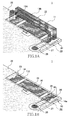
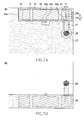
- Fig. 1A is a perspective view showing the configuration of an antenna device 1 according to a first embodiment of the present invention.
- the antenna device 1 has a surface-mounted antenna 10, and a substrate 20 on which the surface-mounted antenna 10 is provided.
- the antenna device 1 is mounted on compact radio communication equipment such as a cellular phone.
- Fig. 1B omits the description of other portions of the surface-mounted antenna 10 so that conductors formed on the bottom surface of the surface-mounted antenna 10 can be easily seen.
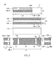
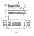
- Fig. 2 shows a developed view of the surface-mounted antenna 10.
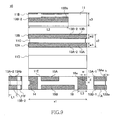
- Figs. 3A and 3B show plan views showing the configuration of the substrate 20.
- FIG. 3A is a plan view of the face side of the substrate 20 (the surface on which the surface-mounted antenna 10 is provided).
- Fig. 3B is a plan view of the back side of the substrate 20. The configuration of the antenna device 1 will be described below in detail with reference to these drawings.
- the surface-mounted antenna 10 has a base 11 made of a dielectric having a substantially rectangular parallelepiped shape, antenna conductor patterns 13A and 13B and plane conductor patterns 14 to 16 configured by conductors on the surface of the base 11. As shown in Fig. 1A , the surface-mounted antenna 10 is provided near the corner portion of the substrate 20.
- the size of the base 11 may be appropriately set according to a target antenna characteristic.
- lateral lengths x1 and x2 (x1 > x2) can be 14 mm and 3 mm, respectively, and a height x3 can be 3 mm.
- dielectric materials such as a Ba-Nd-Ti material (specific inductive capacity of 80 to 120), an Nd-Al-Ca-Ti material (specific inductive capacity of 43 to 46), an Li-Al-Sr-Ti (specific inductive capacity of 38 to 41), a Ba-Ti material (specific inductive capacity of 34 to 36), a Ba-Mg-W material (specific inductive capacity of 20 to 22), an Mg-Ca-Ti material (specific inductive capacity of 19 to 21), sapphire (specific inductive capacity of 9 to 10), alumina ceramics (specific inductive capacity of 9 to 10), and cordierite ceramics (specific inductive capacity of 4 to 6).
- the base 11 is manufactured by calcining these materials using a die.
- the dielectric materials to be specifically used may be appropriately selected according to the used frequencies of the later-described radio communication systems to use the antenna conductor patterns 13A and 13B.
- specific inductive capacity ⁇ r is larger, a higher wavelength shortening effect can be obtained. Therefore, the length of the radiation conductor can be shortened.
- the specific inductive capacity ⁇ r is too large, the antenna gain is reduced. It is preferable to determine the optimum dielectric material by observing the balance of these.
- the Mg-Ca-Ti dielectric ceramic can be preferably used.
- the Mg-Ca-Ti dielectric ceramic it is particularly preferable to use the Mg-Ca-Ti dielectric ceramic containing TiO 2 , MgO, CaO, MnO, and SiO 2 .
- substantially rectangular parallelepiped shape is intended to include, not only a complete rectangular parallelepiped, but also a partially incomplete rectangular parallelepiped.
- a groove which penetrates through the center of each of the surfaces at an equal width and a depth h from the lower side of a side surface 11A through a top surface 11C to the lower side of a side surface 11F is cut in the base 11.
- a convex surface 12A having a constant width w1 along the boundary between the top surface 11C and a side surface 11D and a convex surface 12B having a constant width w2 along the boundary between the top surface 11C and a side surface 11B are formed.
- the base 11 does not have the complete rectangular parallelepiped shape.
- Such groove and convex portions are provided for preferably electrically separating the antenna conductor patterns 13A and 13B.
- the antenna conductor pattern 13A is a conductor pattern formed on the convex surface 12A.
- the formed region of the antenna conductor pattern 13A passes from the lower side of the side surface 11A (of two side surfaces vertical to a longitudinal direction, the side surface near the corner portion of the substrate 20) of the base 11 through the top surface 11C to the position at a distance L1 from the upper side of the side surface 11F (the side surface opposite the side surface 11A), and has a continuous belt-shaped configuration having the constant width w1.
- the portion of the conductor pattern configuring the antenna conductor pattern 13A provided on the side surface 11A is a power supply electrode 13A-1 and the portion other than that is a radiation electrode 13A-2.
- One end 13Aa (the end on the power supply electrode 13A-1 side) of the antenna conductor pattern 13A is connected to the plane conductor pattern 16 at the lower end of the side surface 11A.
- the other end 13Ab (the portion at the distance L1 from the upper side of the side surface 11F) of the antenna conductor pattern 13A is not connected to other conductor patterns.
- the antenna conductor pattern 13B has a conductor pattern formed on the convex surface 12B and a conductor pattern formed on the side surface 11B.
- the former passes from the lower side of the side surface 11A of the base 11 through the top surface 11C to the position at the distance L1 from the upper side of the side surface 11F, and has a continuous belt-shaped configuration having the constant width w2 in parallel with the antenna conductor pattern 13A.
- the latter has a configuration extended from the conductor pattern of the side surface 11F onto the side surface 11B along a length L2.
- the portion of the conductor pattern configuring the antenna conductor pattern 13B provided on the side surface 11A is a power supply electrode 13B-1 and the portion other than that is a radiation electrode 13B-2.
- One end 13Ba (the end on the power supply electrode 13B-1 side) of the antenna conductor pattern 13B is connected to the plane conductor pattern 16 at the lower end of the side surface 11A.
- the other end 13Bb (the portion at the distance L2 from the boundary between the side surfaces 11B and 11F) of the antenna conductor pattern 13B is not connected to other conductor patterns.
- the plane conductor patterns 14 and 16 are conductor patterns having a substantially rectangular shape formed throughout the entire width of a bottom surface 11E at the end on the side surface 11F side and the end on the side surface 11A side in a longitudinal direction of the bottom surface 11E, respectively.
- the length in a longitudinal direction of the base 11 of the plane conductor pattern 16 is L3.
- the plane conductor pattern 14 is extended to the side surfaces 11F and 11B and is not connected to the antenna conductor patterns 13A and 13B.
- the plane conductor pattern 16 is connected to the power supply electrodes 13A-1 and 13B-2 provided on the side surface 11A.
- the plane conductor pattern 16 has a slit 16a having a width w and a depth d cut from the side surface 11D side. This point will be described in detail later.
- the plane conductor pattern 15 is a rectangular conductor pattern formed throughout the entire width of the bottom surface 11E between the plane conductor patterns 14 and 16.
- the plane conductor pattern 15 is extended to near the boundary between the side surface 11B and the bottom surface 11E.
- the plane conductor pattern 15 is not contacted with other conductor patterns on the surface of the base 11.
- Each of the conductor patterns can be formed by sintering under a predetermined temperature condition after applying a paste material for electrode to the base 11 by screen printing or transfer.
- a paste material for electrode silver, silver-palladium, silver-platinum, and copper can be used.
- the conductor pattern can also be formed by plating or sputtering.
- the slit 16a may be manufactured by providing a shape corresponding to the slit 16a in a plate film used for screen printing or may be manufactured by cutting away the portion corresponding to the slit 16a after the plane conductor pattern 16 not having the slit is formed.
- the substrate 20 has, on its face side, a ground clearance region 21 not provided with a ground pattern, a ground pattern 22 provided around the ground clearance region 21, land patterns 23 to 26 provided in the ground clearance region 21, a power supply line 27 connected to the land pattern 25, and a throughhole conductor 28 which guides the power supply line 27 to the back side of the substrate 20, and has, on its back side, a ground pattern 30.
- a region X indicated by the dashed line of the ground clearance region 21 is the provided region of the surface-mounted antenna 10.
- the ground clearance region 21 is provided along the corner portion of the substrate 20. Two directions around the ground clearance region 21 are surrounded by the ground pattern 22. Other two directions form an open space in which the substrate 20 does not exist.
- the ground pattern 30 on the back side also exists immediately below the region X. Therefore, the surface-mounted antenna 10 is of the so-called on-ground type.
- the land patterns 23 and 24 are provided in the positions corresponding to the plane conductor patterns 14 and 15 of the surface-mounted antenna 10, respectively, and are solder connected to these conductors.
- the land pattern 23 is contacted with the ground pattern 22 at an end 23a.
- a chip reactor 29a for frequency adjustment configured by an inductor, a capacitor, or a short circuit is mounted between the land pattern 24 and the ground pattern 22.
- the chip reactor 29a is inserted in series between a lead portion 24a of the land pattern 24 and the ground pattern 22.
- the mounted position of the chip reactor 29a is preferably the position outside the ground clearance region 21 and as closely as possible to the ground clearance region 21.
- the land patterns 25 and 26 are provided in the positions corresponding to the plane conductor pattern 16 of the surface-mounted antenna 10 and are solder connected to these conductors.
- the gap between the land patterns 25 and 26 is set to the constant width w.
- the position of the gap corresponds to the position of the slit 16a.
- the substrate 20 does not have a conductor pattern in a region corresponding to the slit 16a.
- the land pattern 26 is contacted with the ground pattern 22 at an end 26a.
- the power supply line 27 is connected to the land pattern 25.
- a chip reactor 29b for impedance adjustment configured by an inductor, a capacitor, or a short circuit is mounted between the power supply line 27 and the ground pattern 22.
- the mounted position of the chip reactor 29b is preferably the position outside the ground clearance region 21 and as closely as possible to the ground clearance region 21.
- the power supply line 27 is introduced into the back side by the through hole conductor 28 and is connected to a signal line (not shown) on the back side.
- Each of the ground patterns and each of the land patterns can be formed by preparing a substrate to which copper foil is stuck on the entire surface and dissolving the copper foil in the unnecessary portion by etching.
- the antenna conductor patterns 13A and 13B function as an inverted-F antenna, respectively. That is, in the antenna conductor pattern 13A, the land pattern 26 functions as the short stub of the inverted-F antenna, and the end 13Ab functions as the open end of the inverted-F antenna. In the antenna conductor pattern 13B, the land pattern 26 functions as the short stub of the inverted-F antenna and the end 13Bb functions as the open end of the inverted-F antenna.
- the resonance frequencies of the antenna conductor patterns 13A and 13B are determined mainly by the length and width of the conductors formed on the surface of the base 11 and the specific inductive capacity of the base 11. In the antenna device 1, fine adjustment of the resonance frequencies is enabled by appropriately adjusting the reactance of the chip reactor 29a.
- the antenna conductor pattern 13A relatively located inside the substrate 20 is preferably used for the radio communication system of a relatively high frequency.
- the antenna conductor pattern 13B relatively located outside the substrate 20 is preferably used for the radio communication system of a relatively low frequency.
- the resonance frequency of the antenna conductor pattern 13A be adjusted to the 2.5 GHz bandwidth and that the resonance frequency of the antenna conductor pattern 13B be adjusted to the 1.5 GHz bandwidth.
- the slit 16a provided in the plane conductor pattern 16 will be described.
- an electric current input from the power supply line 27 enters the plane conductor pattern 16 through the land pattern 25, and reaches each of the power supply electrodes 13A-1 and 13B-1 beyond the slit 16a.
- the slit 16a is provided between the power supply line 27 and each of the power supply electrodes 13A-1 and 13A-2.
- the depth d of the slit 16a the connection distance between the antenna conductor patterns 13A and 13B and the power supply line 27 can be controlled. This will be specifically described below.
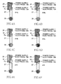
- Figs. 4A, 4B, 4C, 4D, 4E, and 4F are explanatory views of the relation between the connection distance between the antenna conductor patterns 13A or 13B and the power supply line 27 and the depth d of the slit 16a.
- d d 2
- d d 1 (0 ⁇ d 1 ⁇ d 2 )
- d 0.
- the position of the end 26a is fixed.
- a path (power supply path) D A of an electric current from the power supply line 27 to the power supply electrode 13A is longer. This is because the electric current goes around the slit 16a.
- a path D B of an electric current from the power supply line 27 to the power supply electrode 13B is also longer.
- the power supply electrode 13B is substantially opposite the power supply line 27 across the depth direction of the slit 16a, so the amount in change is smaller than that of the path D A .
- the difference between the paths D B and D A can be controlled by changing the depth.
- the impedance matching between the resonance antennas can be simply realized.
- x1 14 mm
- x2 3 mm
- x3 3 mm
- w1 1 mm
- w2 1 mm
- L1 2 mm
- L2 10 mm
- L3 2.5 mm
- d 1 1.5 mm
- d 2 2.5 mm.
- the resonance frequency of the antenna conductor pattern 13A is adjusted to the 2.5 GHz bandwidth.
- the resonance frequency of the antenna conductor pattern 13B is adjusted to the 1.5 GHz bandwidth.
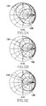
- Figs. 5A, 5B, and 5C are diagrams in which the impedance of each of the antenna conductor patterns 13A and 13B for each of the examples of the depth d shown in Figs. 4A, 4B, 4C, 4D, 4E, and 4F is measured and is shown on the Smith chart.
- the center indicates a reference characteristic impedance (e.g., 50 ⁇ )
- the right end indicates impedance infinity (open)
- the left end indicates impedance 0 (short circuit).
- a positive reactance is taken clockwise of the upper half portion.
- a negative reactance is taken counterclockwise of the lower half portion.
- the impedance of each of the antenna conductor patterns 13A and 13B is traced as shown in the Smith chart of Figs. 5A, 5B, and 5C .
- the impedance characteristic of the antenna conductor pattern 13B is hardly changed according to the depth d.
- the impedance characteristic of the antenna conductor pattern 13A is largely changed according to the depth d. This shows that the impedance of the antenna conductor pattern 13A is particularly controlled by the control of the depth d of the slit 16a.
- Figs. 6A, 6B, 6C, 6D, 6E, and 6F are diagrams in which a return loss near the resonance frequency of each of the antenna conductor patterns 13A and 13B of each of the examples of the depth d shown in Figs. 4A, 4B, 4C, 4D, 4E, and 4F is measured and is plotted.
- Figs. 6A, 6C, and 6E show a return loss near the resonance frequency in the 1.5 GHz bandwidth of the antenna conductor pattern 13B.
- Figs. 6B, 6D, and 6F show a return loss near the resonance frequency in the 2.5 GHz bandwidth of the antenna conductor pattern 13A.
- the return losses are changed according to the depth d of the slit 16a in both the 1.5 GHz bandwidth and the 2.5 GHz bandwidth.
- the magnitude of the change in the 2.5 GHz bandwidth is larger. That is, the difference in impedance between the antenna conductor patterns 13A and 13B is controlled by the control of the depth d of the slit 16a.
- the specific value of the depth d is changed due to various factors of the material, shape, and size of the base 11, the conductor patterns, and the substrate 20, and other elements provided on the substrate 20 and is preferably determined by an experiment for each type of a product.
- the length of the power supply path to each of the antenna conductor patterns can be controlled by adjusting the depth d of the slit 16a. Therefore, the impedance matching between the resonance antennas can be realized by the simple configuration of the slit 16a.
- the antenna device 1 is the same as the first embodiment except for the position providing the slit.
- the slit is provided in the conductor pattern formed on the surface of the surface-mounted antenna 10.
- the slit is provided in the land pattern formed on the surface of the substrate 20. Focusing on this difference, this embodiment will be described below in detail.
- Figs. 7A and 7B are plan views showing the configuration of the substrate 20 according to this embodiment.
- Fig. 8 is a developed view of the surface-mounted antenna 10 according to this embodiment.
- the substrate 20 has a land pattern 31 in place of the land patterns 25 and 26 shown in Fig. 3 .
- the land pattern 31 has a shape in which the gap portion between the land patterns 25 and 26 is filled with the conductor pattern and has a slit 31a having the width w and the depth d cut from the power supply line 27 side in the portion corresponding to the gap.
- the slit 31a may be manufactured by providing a shape corresponding to the slit 31a in a mask used for etching copper foil stuck onto the substrate or may be manufactured by cutting away the portion corresponding to the slit 31a after the land pattern 31 not having the slit is formed.
- the surface-mounted antenna 10 has a plane conductor pattern 17 in place of the plane conductor pattern 16.
- the plane conductor pattern 17 is a substantially rectangular conductor pattern formed throughout the entire width of the bottom surface 11E at the end on the side surface 11A side in a longitudinal direction of the bottom surface 11E, and has a shape in which only the portion on the side surface 11A side from the slit 16a is cut out from the plane conductor pattern 16 shown in Fig. 2 .
- the surface-mounted antenna 10 does not have the conductor pattern in the position corresponding to the slit 31a.
- an electric current input from the power supply line 27 passes through the land pattern 31 beyond the slit 31a to the plane conductor pattern 17.
- the slit 31a is provided between the power supply line 27 and each of the power supply electrodes 13A-1 and 13A-2, as in the slit 16a according to the first embodiment.
- the connection distance between the antenna conductor patterns 13A and 13B and the power supply line 27 is controlled according to the depth d of the slit 31a.
- the length of the power supply path to each of the antenna conductor patterns can be controlled by adjusting the depth d of the slit 31a. Therefore, the impedance matching between the resonance antennas can be realized by the simple configuration of the slit 31a.
- the slit is provided in the substrate 20 side, as compared with the case in which the slit is provided in the surface-mounted antenna 10, the slit can be formed at high accuracy.
- This embodiment is the same as the first embodiment except for the specific configuration of the plane conductor pattern 15. Focusing on this difference, this embodiment will be described below in detail.
- Fig. 9 is a developed view of the surface-mounted antenna 10 according to this embodiment.
- Figs. 10A and 10B are plan views showing the configuration of the substrate 20 according to this embodiment.
- the surface-mounted antenna 10 has plane conductor patterns 15A and 15B in the portion having the plane conductor pattern 15 in the first embodiment (the bottom surface 11E of the base 11).
- the plane conductor pattern 15A has the same width as that of the antenna conductor pattern 13A, and is provided in the position opposite the portion provided on the top surface 11C of the antenna conductor pattern 13A (top surface conductor pattern).
- the plane conductor pattern 15B has the same width as that of the antenna conductor pattern 13B, and is provided in the position opposite the portion provided on the top surface 11C of the antenna conductor pattern 13B (top surface conductor pattern).
- the substrate 20 has land patterns 24A and 24B in place of the land pattern 24.
- the land pattern 24A is provided in the position corresponding to the plane conductor pattern 15A of the surface-mounted antenna 10 and is solder connected to the plane conductor pattern 15A.
- the land pattern 24B is provided in the position corresponding to the plane conductor pattern 15B of the surface-mounted antenna 10 and is solder connected to the plane conductor pattern 15B.
- a chip reactor 29a for frequency adjustment is mounted between the land pattern 24A and the ground pattern 22.
- the chip reactor 29a is inserted in series between a lead portion 24Aa of the land pattern 24A and the ground pattern 22.
- a chip reactor 29c for frequency adjustment is mounted between the land pattern 24B and the ground pattern 22.
- the chip reactor 29c is inserted in series between a lead portion 24Ba of the land pattern 24B and the ground pattern 22.
- the characteristic of the antenna conductor pattern 13A and the characteristic of the antenna conductor pattern 13B can be easily controlled independently. Therefore, the impedance matching between the resonance antennas can be realized more easily.
- the land patterns 24A and 24B are connected to the ground pattern 22 via the chip reactors for adjusting different frequencies (the chip reactors 29a and 29c).
- the frequency can be adjusted for each of the antenna conductor patterns.
Landscapes
- Engineering & Computer Science (AREA)
- Computer Networks & Wireless Communication (AREA)
- Microelectronics & Electronic Packaging (AREA)
- Details Of Aerials (AREA)
- Variable-Direction Aerials And Aerial Arrays (AREA)
- Waveguide Aerials (AREA)
Applications Claiming Priority (1)
| Application Number | Priority Date | Filing Date | Title |
|---|---|---|---|
| JP2008300903A JP4645729B2 (ja) | 2008-11-26 | 2008-11-26 | アンテナ装置、無線通信機、表面実装型アンテナ、プリント基板、並びに表面実装型アンテナ及びプリント基板の製造方法 |
Publications (2)
| Publication Number | Publication Date |
|---|---|
| EP2192653A2 true EP2192653A2 (fr) | 2010-06-02 |
| EP2192653A3 EP2192653A3 (fr) | 2011-08-17 |
Family
ID=41796085
Family Applications (1)
| Application Number | Title | Priority Date | Filing Date |
|---|---|---|---|
| EP09014708A Withdrawn EP2192653A3 (fr) | 2008-11-26 | 2009-11-25 | Antenne assemblée à la surface d'une carte de circuit imprimé et procédé de fabrication |
Country Status (3)
| Country | Link |
|---|---|
| US (1) | US20100127940A1 (fr) |
| EP (1) | EP2192653A3 (fr) |
| JP (1) | JP4645729B2 (fr) |
Cited By (1)
| Publication number | Priority date | Publication date | Assignee | Title |
|---|---|---|---|---|
| EP2648280A1 (fr) * | 2010-11-30 | 2013-10-09 | Mitsubishi Materials Corporation | Dispositif d'antenne |
Families Citing this family (7)
| Publication number | Priority date | Publication date | Assignee | Title |
|---|---|---|---|---|
| JP5375719B2 (ja) * | 2010-04-01 | 2013-12-25 | Tdk株式会社 | アンテナ装置及びこれを用いた無線通信機 |
| JP4938158B2 (ja) | 2010-06-07 | 2012-05-23 | 新日本製鐵株式会社 | 鋼レールおよびその製造方法 |
| JP5251965B2 (ja) * | 2010-11-22 | 2013-07-31 | Tdk株式会社 | アンテナ装置及びその周波数調整方法 |
| JP5561615B2 (ja) * | 2011-01-18 | 2014-07-30 | 三菱マテリアル株式会社 | アンテナ装置 |
| US8970436B2 (en) * | 2013-03-14 | 2015-03-03 | Circomm Technology Corp. | Surface mount device multi-frequency antenna module |
| JP7298505B2 (ja) | 2020-02-19 | 2023-06-27 | 株式会社デンソー | アンテナ装置 |
| JP7298517B2 (ja) | 2020-03-05 | 2023-06-27 | 株式会社デンソー | 電子装置 |
Citations (1)
| Publication number | Priority date | Publication date | Assignee | Title |
|---|---|---|---|---|
| JP3319268B2 (ja) | 1996-02-13 | 2002-08-26 | 株式会社村田製作所 | 表面実装型アンテナおよびこれを用いた通信機 |
Family Cites Families (14)
| Publication number | Priority date | Publication date | Assignee | Title |
|---|---|---|---|---|
| JPH1127041A (ja) * | 1997-07-03 | 1999-01-29 | F Ii C:Kk | 携帯通信端末用のアンテナ |
| JP2001127525A (ja) * | 1999-08-18 | 2001-05-11 | Alps Electric Co Ltd | アンテナ |
| JP2001177330A (ja) * | 1999-12-17 | 2001-06-29 | Tdk Corp | パッチアンテナ |
| JP3658639B2 (ja) * | 2000-04-11 | 2005-06-08 | 株式会社村田製作所 | 表面実装型アンテナおよびそのアンテナを備えた無線機 |
| TW513829B (en) * | 2000-10-12 | 2002-12-11 | Furukawa Electric Co Ltd | Small antenna |
| DE60223515T2 (de) * | 2001-03-15 | 2008-09-18 | Matsushita Electric Industrial Co., Ltd., Kadoma | Antennenvorrichtung |
| JP4044302B2 (ja) * | 2001-06-20 | 2008-02-06 | 株式会社村田製作所 | 表面実装型アンテナおよびそれを用いた無線機 |
| JP3931866B2 (ja) * | 2002-10-23 | 2007-06-20 | 株式会社村田製作所 | 表面実装型アンテナおよびそれを用いたアンテナ装置および通信装置 |
| JP3812531B2 (ja) * | 2002-11-13 | 2006-08-23 | 株式会社村田製作所 | 面実装型アンテナおよびその製造方法および通信装置 |
| EP1643588B1 (fr) * | 2003-07-08 | 2008-02-13 | Matsushita Electric Industrial Co., Ltd. | Poste de radio portatif |
| WO2006073034A1 (fr) * | 2005-01-05 | 2006-07-13 | Murata Manufacturing Co., Ltd. | Structure d’antenne et unité de communication sans fil équipée de celle-ci |
| WO2006120763A1 (fr) * | 2005-05-13 | 2006-11-16 | Murata Manufacturing Co., Ltd. | Structure d’antenne et dispositif de communication radio utilisant ladite structure d’antenne |
| JP4775233B2 (ja) * | 2006-11-16 | 2011-09-21 | Tdk株式会社 | アンテナ装置及びそれを用いたアンテナ実装基板 |
| JP5056846B2 (ja) * | 2007-03-29 | 2012-10-24 | 株式会社村田製作所 | アンテナおよび無線通信機 |
-
2008
- 2008-11-26 JP JP2008300903A patent/JP4645729B2/ja not_active Expired - Fee Related
-
2009
- 2009-11-23 US US12/623,911 patent/US20100127940A1/en not_active Abandoned
- 2009-11-25 EP EP09014708A patent/EP2192653A3/fr not_active Withdrawn
Patent Citations (1)
| Publication number | Priority date | Publication date | Assignee | Title |
|---|---|---|---|---|
| JP3319268B2 (ja) | 1996-02-13 | 2002-08-26 | 株式会社村田製作所 | 表面実装型アンテナおよびこれを用いた通信機 |
Cited By (3)
| Publication number | Priority date | Publication date | Assignee | Title |
|---|---|---|---|---|
| EP2648280A1 (fr) * | 2010-11-30 | 2013-10-09 | Mitsubishi Materials Corporation | Dispositif d'antenne |
| EP2648280A4 (fr) * | 2010-11-30 | 2014-08-06 | Mitsubishi Materials Corp | Dispositif d'antenne |
| US9142884B2 (en) | 2010-11-30 | 2015-09-22 | Mitsubishi Materials Corporation | Antenna device |
Also Published As
| Publication number | Publication date |
|---|---|
| JP4645729B2 (ja) | 2011-03-09 |
| EP2192653A3 (fr) | 2011-08-17 |
| US20100127940A1 (en) | 2010-05-27 |
| JP2010130164A (ja) | 2010-06-10 |
Similar Documents
| Publication | Publication Date | Title |
|---|---|---|
| EP2192653A2 (fr) | Dispositif d'antenne, équipement de communication radio, antenne assemblée à la surface, carte de circuit imprimé, et procédé de fabrication d'antenne assemblée en surface et la carte de circuit imprimé | |
| EP2226891B1 (fr) | Dispositif d'antenne et élément d'antenne utilisé avec celui-ci | |
| KR101139741B1 (ko) | 안테나 장치 및 이것을 사용한 무선 통신기 | |
| JP5333235B2 (ja) | アンテナ装置及びこれを用いた無線通信機 | |
| JP4867787B2 (ja) | アンテナ装置 | |
| US8279133B2 (en) | Antenna device | |
| JP2005167762A (ja) | 誘電体アンテナおよびそれを用いた通信機能を有する電気機器 | |
| US9225057B2 (en) | Antenna apparatus and wireless communication device using same | |
| JPH05259724A (ja) | プリントアンテナ | |
| US8384598B2 (en) | Surface-mounted antenna, antenna device using the same, and radio communication equipment | |
| JP2005086788A (ja) | 表面実装型アンテナおよびアンテナ装置ならびに無線通信装置 | |
| JP4848992B2 (ja) | アンテナ装置及びこれを用いた無線通信機器 | |
| JP4924399B2 (ja) | アンテナ装置及びこれを用いた無線通信機 | |
| JP4775298B2 (ja) | アンテナ装置及びこれを用いた無線通信機器 | |
| JP4894502B2 (ja) | アンテナ装置 | |
| JP2008252155A (ja) | アンテナ装置及びこれを用いた無線通信機器 | |
| KR20110003679A (ko) | 접지면 패치를 이용한 모노폴 칩 안테나 | |
| JP2008252158A (ja) | アンテナブロック、アンテナ装置及び無線通信機器 | |
| JP2016116145A (ja) | アンテナ素子、アンテナ装置及びこれを用いた無線通信機器 | |
| JP2009239538A (ja) | アンテナ装置 |
Legal Events
| Date | Code | Title | Description |
|---|---|---|---|
| PUAI | Public reference made under article 153(3) epc to a published international application that has entered the european phase |
Free format text: ORIGINAL CODE: 0009012 |
|
| AK | Designated contracting states |
Kind code of ref document: A2 Designated state(s): AT BE BG CH CY CZ DE DK EE ES FI FR GB GR HR HU IE IS IT LI LT LU LV MC MK MT NL NO PL PT RO SE SI SK SM TR |
|
| AX | Request for extension of the european patent |
Extension state: AL BA RS |
|
| RTI1 | Title (correction) |
Free format text: SURFACE-MOUNTED ANTENNA ON A PRINTED CIRCUIT BOARD, AND MANUFACTURING METHOD THEREOF |
|
| PUAL | Search report despatched |
Free format text: ORIGINAL CODE: 0009013 |
|
| AK | Designated contracting states |
Kind code of ref document: A3 Designated state(s): AT BE BG CH CY CZ DE DK EE ES FI FR GB GR HR HU IE IS IT LI LT LU LV MC MK MT NL NO PL PT RO SE SI SK SM TR |
|
| AX | Request for extension of the european patent |
Extension state: AL BA RS |
|
| RIC1 | Information provided on ipc code assigned before grant |
Ipc: H01Q 9/42 20060101ALI20110713BHEP Ipc: H01Q 1/24 20060101ALI20110713BHEP Ipc: H01Q 1/38 20060101ALI20110713BHEP Ipc: H01Q 9/04 20060101AFI20110713BHEP |
|
| STAA | Information on the status of an ep patent application or granted ep patent |
Free format text: STATUS: THE APPLICATION HAS BEEN WITHDRAWN |
|
| 18W | Application withdrawn |
Effective date: 20120214 |