EP2157668A1 - Verbinder und metallmaterial für einen verbinder - Google Patents
Verbinder und metallmaterial für einen verbinder Download PDFInfo
- Publication number
- EP2157668A1 EP2157668A1 EP08739527A EP08739527A EP2157668A1 EP 2157668 A1 EP2157668 A1 EP 2157668A1 EP 08739527 A EP08739527 A EP 08739527A EP 08739527 A EP08739527 A EP 08739527A EP 2157668 A1 EP2157668 A1 EP 2157668A1
- Authority
- EP
- European Patent Office
- Prior art keywords
- alloy
- layer
- connector
- metallic material
- plating layer
- Prior art date
- Legal status (The legal status is an assumption and is not a legal conclusion. Google has not performed a legal analysis and makes no representation as to the accuracy of the status listed.)
- Granted
Links
Images


Classifications
-
- H—ELECTRICITY
- H01—ELECTRIC ELEMENTS
- H01R—ELECTRICALLY-CONDUCTIVE CONNECTIONS; STRUCTURAL ASSOCIATIONS OF A PLURALITY OF MUTUALLY-INSULATED ELECTRICAL CONNECTING ELEMENTS; COUPLING DEVICES; CURRENT COLLECTORS
- H01R13/00—Details of coupling devices of the kinds covered by groups H01R12/70 or H01R24/00 - H01R33/00
- H01R13/02—Contact members
- H01R13/03—Contact members characterised by the material, e.g. plating, or coating materials
-
- C—CHEMISTRY; METALLURGY
- C25—ELECTROLYTIC OR ELECTROPHORETIC PROCESSES; APPARATUS THEREFOR
- C25D—PROCESSES FOR THE ELECTROLYTIC OR ELECTROPHORETIC PRODUCTION OF COATINGS; ELECTROFORMING; APPARATUS THEREFOR
- C25D5/00—Electroplating characterised by the process; Pretreatment or after-treatment of workpieces
- C25D5/10—Electroplating with more than one layer of the same or of different metals
-
- C—CHEMISTRY; METALLURGY
- C25—ELECTROLYTIC OR ELECTROPHORETIC PROCESSES; APPARATUS THEREFOR
- C25D—PROCESSES FOR THE ELECTROLYTIC OR ELECTROPHORETIC PRODUCTION OF COATINGS; ELECTROFORMING; APPARATUS THEREFOR
- C25D5/00—Electroplating characterised by the process; Pretreatment or after-treatment of workpieces
- C25D5/48—After-treatment of electroplated surfaces
- C25D5/50—After-treatment of electroplated surfaces by heat-treatment
-
- C—CHEMISTRY; METALLURGY
- C25—ELECTROLYTIC OR ELECTROPHORETIC PROCESSES; APPARATUS THEREFOR
- C25D—PROCESSES FOR THE ELECTROLYTIC OR ELECTROPHORETIC PRODUCTION OF COATINGS; ELECTROFORMING; APPARATUS THEREFOR
- C25D5/00—Electroplating characterised by the process; Pretreatment or after-treatment of workpieces
- C25D5/60—Electroplating characterised by the structure or texture of the layers
- C25D5/623—Porosity of the layers
-
- C—CHEMISTRY; METALLURGY
- C25—ELECTROLYTIC OR ELECTROPHORETIC PROCESSES; APPARATUS THEREFOR
- C25D—PROCESSES FOR THE ELECTROLYTIC OR ELECTROPHORETIC PRODUCTION OF COATINGS; ELECTROFORMING; APPARATUS THEREFOR
- C25D7/00—Electroplating characterised by the article coated
-
- H—ELECTRICITY
- H01—ELECTRIC ELEMENTS
- H01R—ELECTRICALLY-CONDUCTIVE CONNECTIONS; STRUCTURAL ASSOCIATIONS OF A PLURALITY OF MUTUALLY-INSULATED ELECTRICAL CONNECTING ELEMENTS; COUPLING DEVICES; CURRENT COLLECTORS
- H01R43/00—Apparatus or processes specially adapted for manufacturing, assembling, maintaining, or repairing of line connectors or current collectors or for joining electric conductors
- H01R43/16—Apparatus or processes specially adapted for manufacturing, assembling, maintaining, or repairing of line connectors or current collectors or for joining electric conductors for manufacturing contact members, e.g. by punching and by bending
-
- C—CHEMISTRY; METALLURGY
- C25—ELECTROLYTIC OR ELECTROPHORETIC PROCESSES; APPARATUS THEREFOR
- C25D—PROCESSES FOR THE ELECTROLYTIC OR ELECTROPHORETIC PRODUCTION OF COATINGS; ELECTROFORMING; APPARATUS THEREFOR
- C25D3/00—Electroplating: Baths therefor
- C25D3/02—Electroplating: Baths therefor from solutions
- C25D3/30—Electroplating: Baths therefor from solutions of tin
-
- C—CHEMISTRY; METALLURGY
- C25—ELECTROLYTIC OR ELECTROPHORETIC PROCESSES; APPARATUS THEREFOR
- C25D—PROCESSES FOR THE ELECTROLYTIC OR ELECTROPHORETIC PRODUCTION OF COATINGS; ELECTROFORMING; APPARATUS THEREFOR
- C25D3/00—Electroplating: Baths therefor
- C25D3/02—Electroplating: Baths therefor from solutions
- C25D3/38—Electroplating: Baths therefor from solutions of copper
-
- H—ELECTRICITY
- H01—ELECTRIC ELEMENTS
- H01R—ELECTRICALLY-CONDUCTIVE CONNECTIONS; STRUCTURAL ASSOCIATIONS OF A PLURALITY OF MUTUALLY-INSULATED ELECTRICAL CONNECTING ELEMENTS; COUPLING DEVICES; CURRENT COLLECTORS
- H01R13/00—Details of coupling devices of the kinds covered by groups H01R12/70 or H01R24/00 - H01R33/00
- H01R13/02—Contact members
- H01R13/04—Pins or blades for co-operation with sockets
-
- H—ELECTRICITY
- H01—ELECTRIC ELEMENTS
- H01R—ELECTRICALLY-CONDUCTIVE CONNECTIONS; STRUCTURAL ASSOCIATIONS OF A PLURALITY OF MUTUALLY-INSULATED ELECTRICAL CONNECTING ELEMENTS; COUPLING DEVICES; CURRENT COLLECTORS
- H01R13/00—Details of coupling devices of the kinds covered by groups H01R12/70 or H01R24/00 - H01R33/00
- H01R13/02—Contact members
- H01R13/10—Sockets for co-operation with pins or blades
- H01R13/11—Resilient sockets
- H01R13/113—Resilient sockets co-operating with pins or blades having a rectangular transverse section
-
- Y—GENERAL TAGGING OF NEW TECHNOLOGICAL DEVELOPMENTS; GENERAL TAGGING OF CROSS-SECTIONAL TECHNOLOGIES SPANNING OVER SEVERAL SECTIONS OF THE IPC; TECHNICAL SUBJECTS COVERED BY FORMER USPC CROSS-REFERENCE ART COLLECTIONS [XRACs] AND DIGESTS
- Y10—TECHNICAL SUBJECTS COVERED BY FORMER USPC
- Y10T—TECHNICAL SUBJECTS COVERED BY FORMER US CLASSIFICATION
- Y10T428/00—Stock material or miscellaneous articles
- Y10T428/12—All metal or with adjacent metals
- Y10T428/12458—All metal or with adjacent metals having composition, density, or hardness gradient
-
- Y—GENERAL TAGGING OF NEW TECHNOLOGICAL DEVELOPMENTS; GENERAL TAGGING OF CROSS-SECTIONAL TECHNOLOGIES SPANNING OVER SEVERAL SECTIONS OF THE IPC; TECHNICAL SUBJECTS COVERED BY FORMER USPC CROSS-REFERENCE ART COLLECTIONS [XRACs] AND DIGESTS
- Y10—TECHNICAL SUBJECTS COVERED BY FORMER USPC
- Y10T—TECHNICAL SUBJECTS COVERED BY FORMER US CLASSIFICATION
- Y10T428/00—Stock material or miscellaneous articles
- Y10T428/12—All metal or with adjacent metals
- Y10T428/12493—Composite; i.e., plural, adjacent, spatially distinct metal components [e.g., layers, joint, etc.]
- Y10T428/12708—Sn-base component
- Y10T428/12715—Next to Group IB metal-base component
-
- Y—GENERAL TAGGING OF NEW TECHNOLOGICAL DEVELOPMENTS; GENERAL TAGGING OF CROSS-SECTIONAL TECHNOLOGIES SPANNING OVER SEVERAL SECTIONS OF THE IPC; TECHNICAL SUBJECTS COVERED BY FORMER USPC CROSS-REFERENCE ART COLLECTIONS [XRACs] AND DIGESTS
- Y10—TECHNICAL SUBJECTS COVERED BY FORMER USPC
- Y10T—TECHNICAL SUBJECTS COVERED BY FORMER US CLASSIFICATION
- Y10T428/00—Stock material or miscellaneous articles
- Y10T428/12—All metal or with adjacent metals
- Y10T428/12493—Composite; i.e., plural, adjacent, spatially distinct metal components [e.g., layers, joint, etc.]
- Y10T428/12708—Sn-base component
- Y10T428/12722—Next to Group VIII metal-base component
Definitions
- the present invention relates to a connector that is comprised of a male terminal and a female terminal, and relates to a metallic material to be made use for such the connector.
- a male terminal and a female terminal for such as a connector to be made use for a connection to between an electric wire in a motor vehicle or the like, in which there are provided a metal covering layer of such as a tin (Sn) or an alloy of tin or the like on an electrically conductive substrate (refer to as a substrate properly hereinafter) of such as an alloy of copper (Cu) or the like.
- such the male terminal and the female terminal are individually housed in a housing, and then each of such the terminals is configured as a male connector and a female connector respectively.
- a metallic material as a high performance electric conductor that has a substrate which is superior in the electrical conductivity and a strength thereof, that has a metal covering layer which is superior in an electrical connectability and a corrosion resistance and in a solderability thereon, that is to be made use for a material of the male terminal and for a material of the female terminal, in which there is provided the metal covering layer of such as Sn or the alloy of Sn or the like on the electrically conductive substrate of such as Cu or the alloy of Cu or the like by making use of such as a plating or the like (refer to the following Patent Document 1 to 4 for example).
- the metallic material in general, there is designed to be formed an underlayer of nickel (Ni) or cobalt (Co) or of iron (Fe) or the like by making use of such as the plating or the like, that individually have a barrier function in order to prevent an alloy content of such as zinc (Zn) or the like in the substrate (refer to as a substrate element properly hereinafter) from diffusing into the above mentioned metal covering layer.
- Ni nickel
- Co cobalt
- Fe iron
- an oxide film layer on a surface of such the metal covering layer of such as Sn or the like on a surface of the terminal due to the Sn thereon as easier to be oxidized under an environment at a temperature as higher, such as at an inside of an engine room of the motor vehicle or the like. And then due to such the oxide film layer as short, it is able to obtain an electrical connectability of therebetween as excellently because such the oxide film layer becomes to be torn thereby at a time of a connection of the terminal thereto, and then because there becomes to be exposed unoxygenated Sn from an inside of an under layered metal covering layer.
- such the above mentioned fretting phenomenon is the phenomenon that a plating layer of Sn as a soft layer on a surface of a terminal becomes to be worn away and to be oxidized and then to be a abrasion powder that has a specific resistance as larger, due to a slight sliding that is generated on between the contact faces of the individual terminals because of such as a vibration thereon or variation of a temperature thereof or the like. And then thereby there becomes to be occurred the failure in connection of therebetween in the case where there is occurred such the phenomenon at between each of the terminals. Further, the lower the pressure of the contact to between each of the terminals the easier there becomes to be occurred such the phenomenon. Still further, there may become to be difficult for such the phenomenon to occur by designing a thickness of the plating layer of Sn as thinner on each of the surfaces of the individual terminals in the connector, however, it is difficult to prevent completely from occurring such the phenomenon.
- the metallic material in which there is designed to be provided a layer of Ni in between the above mentioned substrate and the intermetallic compound layer of Cu-Sn in order to prevent from the diffusion of any elements from the substrate (refer to the following Patent Document 7 for example).
- Patent Document 7 for example.
- a connector that is comprised of a male terminal and a female terminal and able to provide a metallic material to be made use therefor as defined below.
- a connector in accordance with the present invention is the connector in which there are designed to be arranged a male connector that comprises a male terminal and to be arranged a female connector that comprises a female terminal as connectable with each other, and that there is designed to be formed a most surface layer on at least one of such the male terminal and the female terminal with making use of a metallic material as an alloy layer of Cu-Sn. Moreover, there are designed to be arranged such the male terminals as not less than one in general by being housed individually in a housing (not shown in any of the figures) regarding the male connector that comprises such the male terminal.
- the above mentioned metallic material as preferably by performing a plating of an element, such as Ni or Cu or Sn or the like as principally, onto such as an electrically conductive base material or the like.
- a plating of an element such as Ni or Cu or Sn or the like as principally
- an electrically conductive base material or the like such as an electrically conductive base material or the like.
- a configuration of the individual thicknesses of the plating thereon, whether or not performing a process of a heat treatment therefor, an amount of time at a temperature of the process of the heat treatment therefor in a case of performing such the process of the heat treatment therefor, whether or not performing a process of cooling therefor, an amount of time for performing the process of cooling therefor in a case of performing such the process of cooling therefor, or the like it is designed therefor individually to be set as properly with corresponding to a manufacturing cost in total and with corresponding to quality of a part as required that is to be made use therefor.
- FIG. 1 is a diagrammatic perspective view for showing a male terminal 10 in a connector regarding one embodiment in accordance with the present invention.
- the male terminal 10 comprises a tab 11 as a part for connecting with a female terminal 20 and a wire barrel 12 as a part for jointing by pressing in order to perform a jointing by pressing with an electric wire.
- the tab 11 is designed to be formed as a flat plate shape, and then there is designed to be finished the same with an upper surface thereof and a lower surface thereof to be the individual surfaces as smooth respectively.
- FIG. 2 is a diagrammatic perspective view for showing an internal structure of a female terminal 20 in the connector regarding one embodiment in accordance with the present invention. And then such the male terminal 10 as shown in FIG. 1 and the female terminal 20 as shown in FIG. 2 are designed to be as connectable with reach other and designed to comprise the connector therein. Still further, a contact member part in the female terminal 20 for the male terminal 10 in accordance with FIG. 2 is designed to be as a hollow box type, and then there is provided a ligulate piece 21 and a dimple 22 and a bead 23 at an inner side thereof.
- such the dimple 22 is the member of convex shape that is designed to be arranged on an upper part of the ligulate piece 21, and then that is designed to be point contacted with a lower surface of the tab 11 at a period of the connection to the male terminal 10.
- such the ligulate piece 21 is designed to have a function as a spring to function a contact pressure, that is to say, a pressure to push the dimple 22 toward the tab 11.
- the bead 23 is the member of convex shape as well, and then that is designed to be contacted to the upper surface of the tab 11 and then to be received the contact pressure of which such the dimple 22 forces toward the tab 11.
- a most surf ace thereof is designed to be formed with making use of a metallic material as an alloy layer of Cu-Sn. Moreover, there may be designed to be formed only a part of the male terminal 10 and/or of the female terminal 20 with making use of the above mentioned metallic material. And then it is desirable to be formed at least the contact member part with making use of the above mentioned metallic material in such the case thereof.
- the male terminal 10 it is desirable only for the male terminal 10 to be as the alloy of Cu-Sn rather than only for the female terminal 20 to comprise the alloy layer of Cu-Sn in a case where there is designed to be formed the most surface layer on either one of the male terminal 10 or the female terminal 20 with making use of the metallic material as the alloy layer of Cu-Sn. And then it is further preferable for both of the male terminal 10 and the female terminal 20 to be as the alloy of Cu-Sn.
- a state of the most surface layer of the metallic material is defined here to be as an initial state for a connector in a case where such the metallic material is designed to be made use for the connector in accordance with the present invention.
- the softer surface thereof becomes to be rubbed worn away easier, and then the smaller an amount of such the part to be worn away the smaller the force for inserting thereinto.
- a male terminal and a female terminal that are connectable to each other, and there is designed to be formed all over a surface of the terminal regarding either one of the above mentioned male terminal or the above mentioned female terminal or to be formed at least a contact member part of the same with making use of a metallic material on which a most surface thereof is designed to be comprised of an alloy layer of Cu-Sn, and also there is designed to be formed at least a contact member part of the other one of the above mentioned male terminal or the above mentioned female terminal with making use of a metallic material on which a most surface thereof is designed to be comprised of a layer of Sn or an alloy layer of Sn.
- the male terminal there may be a probability to occur with an area as larger regarding the fretting phenomenon or a forming of a pure layer of Sn which is a cause of the force for inserting thereinto as higher, due to the contact member part thereof as a flat plate shape.
- the area thereof becomes to be smaller due to the contact member part thereof as a hemispherical shape. Therefore, it is desirable for the above mentioned most surface of the male terminal to be comprised of the alloy layer of Cu-Sn, and for the above mentioned most surface of the female terminal to be comprised of the layer of Sn or of the alloy layer of Sn.
- the male terminal to be as the terminal that has the surface to be harder as the side for the above mentioned contact member part thereof to have the contact area as larger
- the female terminal to be as the terminal that has the surface to be softer as the side for the above mentioned contact member part thereof to have the contact area as smaller, with taking into consideration of the locus of such the individual contact member parts for each of the male terminal and the female terminal at the period of the connection to therebetween. And then thereby it becomes able to reduce the amount of the part to be worn away (per a unit area) from the surface for such the contact member part thereof to have the contact area as larger, and hence it becomes able to enhance the effect of reducing the force for inserting thereinto.
- the male terminal in general with having the flat shape in order to insert with ease thereinto.
- the female terminal on the contrary thereto with having a shape by which the same become to have a function as a spring by being performed a process of bending work onto either one of an upper side of an inner surface thereof or a lower side thereof or both of such the sides thereof.
- the contact member part at the side on the female terminal as being protruded toward the side on the male terminal in general.
- such the connector is designed for such the connector to be mounted onto a motor vehicle as a connector for being mounted on a motor vehicle for instance.
- the usage of such the connector in accordance with the present invention is not limited to the connector for being mounted on a motor vehicle, and then it is possible to apply the same to any connector for any other usage of such as an electrical device or an electronic device or the like.
- the metallic material for the connector in accordance with the present invention is the metallic material to form at least a part of a male terminal or a part of a female terminal in an electrical device or in an electronic device, in which there is provided an alloy layer of Cu-Sn on a most surface thereof.
- an alloy layer of Cu-Sn on a most surface thereof.
- FIG. 4 is a drawing from a diagrammatic perspective view for showing a metallic material for a connector regarding one embodiment as preferably in accordance with the present invention, wherein such the metallic material for the connector 5 comprises an electrically conductive substrate 1, an underlayer 2 which is comprised of Ni and is provided thereto, an intermediate layer 3 which is comprised of Cu and is provided thereto, and an alloy layer of Cu-Sn 4 which is provided thereto.
- the metallic material for the connector 5 comprises an electrically conductive substrate 1, an underlayer 2 which is comprised of Ni and is provided thereto, an intermediate layer 3 which is comprised of Cu and is provided thereto, and an alloy layer of Cu-Sn 4 which is provided thereto.
- such the metallic material for the connector 5 is designed to be produced by such as the following processes of: performing a process of plating for forming a layer of Ni (an N-layer) 2a, a layer of Cu (a C-layer) 3a and a layer of Sn (an S-layer) 4a in order onto an electrically conductive substrate 1 as shown in a drawing from a diagrammatic perspective view of FIG. 5 in order to form a layered body by plating 6; performing each of the diffusions of the Cu in the above mentioned C-layer 3a and the Sn in the above mentioned S-layer 4a by performing a process of treating with heat therefor; and then forming an alloy layer of Cu-Sn on a most surface thereof by performing a reaction therebetween.
- a thickness of the above mentioned C-layer 3a (the thickness of the intermediate layer 3) in particular therein after performing the process of treating with heat therefor to be specified as strictly on the contrary thereto. And hence it becomes able to perform as easily the designing of the layered body by plating 6 and to perform the process of treating with heat therefor. And therefore it becomes able to obtain the metallic material for the connector 5 in accordance with the present invention with an ease of the production therefor and with being superior in productivity thereof.
- a thickness of the C-layer 3a in the layered body by plating 6 is designed for a thickness of the C-layer 3a in the layered body by plating 6 to be as not less than 0.01 ⁇ m in general. Moreover, it is desirable for an upper limit therefor to be as approximately 5.0 ⁇ m, with taking into consideration of such as a point of view of a practical aspect thereof, a cost of the materials therefor, a cost of the production therefor, or the like. Further, it is further preferable for such the thickness of the C-layer 3a therein to be as not thinner than 0.05 ⁇ m but not thicker than 0.5 ⁇ m.
- micro-pores as a large number thereof in the C-layer (intermediate layer 3) after performing the process of treating with heat therefor in a case where there is designed to be made use of Cu for such the C-layer 3a and then where such the Cu layer 3a is thinner therein. And then thereby there may be a case to be happened that the barrier function as the intermediate layer is lost therefrom. And hence it is further preferable for such the thickness of the C-layer 3a to be as slightly thicker in the case where there is designed to be made use of Cu, which is compared to that in a case where there is designed to be made use of an alloy of Cu therefor.
- the S-layer 4a in accordance with the present invention it is required an amount of time as longer with depending on a thickness thereof for such the S-layer 4a to be reacted completely therein. And then after a process of treating with heat therefor there may be a case where the Sn therein is diffused into the alloy of Cu-Sn 4 and then is remained therein with having a punctuate shape or an island shape. However, there is seldom happened for the function of the metallic material for the connector 5 to be worsened due to such the case thereof. Moreover, there may be a case where a part of the Sn or the alloy of Sn that is diffused thereinto becomes to be exposed onto the surface of the alloy layer of Cu-Sn 4 in such the above mentioned case thereof. And then in such the case thereof it is desirable for an exposed area of the Sn or of the alloy of Sn that is exposed thereto to be as sufficiently smaller comparing to an area of the faces in total of the Sn or the alloy of Sn that is diffused thereinto.
- the diffused Sn thereinto it becomes possible for the diffused Sn thereinto to react with such the excessive amount thereof and then to further diffuse such the Sn thereinto in such the case where there is designed to be diffused such the Sn into the alloy layer of Cu-Sn 4 as the most surface layer even if there is designed to be remained the Cu layer (intermediate layer) 3 as thicker. Furthermore, an effect of such the diffusion thereinto is remarkable under an environment with a temperature as higher. And hence it becomes possible to obtain a domain for a designing of condition as wider regarding the plating thereon and the production thereof, and then thereby it becomes possible to maintain the individual properties thereof with an amount of time for longer even under such the environment with the temperature as higher.
- the above mentioned material in which the Sn or the alloy of Sn is designed to be diffused into the alloy layer of Cu-Sn 4 is one embodiment regarding the metallic material in accordance with the present invention as well.
- the Sn or the alloy of Sn that is diffused as the punctuate shape or as the island shape from the point of view of cross section is defined that a rate of occupation regarding an area of the Sn or of the alloy of Sn in the alloy layer of Cu-Sn, which is approximately equivalent to a rate of occupation regarding a volume thereof, to be as between zero percent and sixty percent in accordance with an image by mapping that is obtained by making use of such as an instrument of an Auger electron spectroscopy (AES) or the like.
- AES Auger electron spectroscopy
- FIG. 6 through FIG. 10 is a picture for showing an image by mapping that is obtained by making use of the instrument of the AES for one sample regarding the metallic material in accordance with the present invention.
- the sample with an oblique section of thirty degrees by making use of a focused ion beam (FIB) with setting such the sample to be inclined as sixty degrees, and such the sample is assumed to be as a sample for an Auger analysis and measurement (AES).
- FIB focused ion beam
- AES Auger analysis and measurement
- each of such the electron images of the AES therein therein.
- the alloy layer of Cu-Sn as the most surface layer thereon that there is existed an intermetallic compound of Cu-Sn together therewith, such as Cu 6 Sn 5 or Cu 3 Sn or Cu 4 Sn or the like.
- FIG. 6 is an SEM photograph (having a width of 11.7 ⁇ m) for showing a measuring region of the AES measurement therefor on a cross section of the sample.
- each of FIG. 7 through FIG. 10 is a picture for showing an image by mapping regarding a metallographic structure of the measuring region thereof as shown in FIG. 6 .
- FIG. 7 is an Sn-Cu-Ni map for showing the Sn therein, the Cu therein and the Ni therein with making use of lightness and darkness of color as different from each other
- FIG. 8 is an Sn map for showing the Sn therein with making use of white color
- FIG. 9 is a Cu map for showing the Cu therein with making use of white color
- FIG. 10 is an Ni map for showing the Ni therein with making use of white color.
- the symbol of 31 designates a surface of the alloy layer of Cu-Sn (outermost layer) in accordance with each of FIG. 7 through FIG. 10
- the symbol of 32 designates a substrate therein
- the symbol of 33 designates an underlayer therein
- the symbol of 34 designates an intermediate layer therein
- the symbol of 35 designates the alloy layer of Cu-Sn (outermost layer) therein.
- the alloy layer of Cu-Sn 35 with making use of white color in accordance with FIG. 8 , and then a part at a side for the surface 31 as further brighter indicates that there is contained Sn therein as a larger number thereof.
- the underlayer 33 with making use of black color in accordance with FIG.
- each of FIG. 11 through FIG. 15 is a picture for showing an image by mapping for another sample regarding the other metallic material in accordance with the present invention, which is obtained by making use of the instrument of the AES as similar to that in accordance with each of FIG. 7 through FIG. 10 .
- FIG. 11 is an SEM photograph (having a width of 11.7 ⁇ m) for showing a measuring region of the AES measurement therefor on a cross section of the sample.
- each of FIG. 12 through FIG. 15 is a picture for showing an image by mapping regarding a metallographic structure of the measuring region thereof as shown in FIG. 11 .
- FIG. 11 is an SEM photograph (having a
- FIG. 12 is an Sn-Cu-Ni map for showing the Sn therein, the Cu therein and the Ni therein with making use of lightness and darkness of color as different from each other
- FIG. 13 is an Sn map for showing the Sn therein with making use of white color
- FIG. 14 is a Cu map for showing the Cu therein with making use of white color
- FIG. 15 is an Ni map for showing the Ni therein with making use of white color.
- the symbol of 31 designates a surface of the alloy layer of Cu-Sn in accordance with each of FIG. 11 through FIG.
- the symbol of 32 designates a substrate therein
- the symbol of 33 designates an underlayer therein
- the symbol of 34 designates an intermediate layer therein
- the symbol of 35 designates the alloy layer of Cu-Sn therein.
- Sn or an alloy of Sn 36 to be diffused as an island shape into the alloy layer of Cu-Sn 35 in accordance with FIG. 12 as shown with making use of a further darker color therein.
- the alloy layer of Cu-Sn 35 as further brighter in accordance with FIG. 13 , and then which indicates that there is contained the Sn or the alloy of Sn 36 in a part as an island shape with making use of a further white color at a side for the surface 31 thereof.
- underlayer 33 and the Sn or the alloy of Sn 36 as an island shape in accordance with FIG. 14 , and then which indicates that there is not contained substantially any Cu in each of such the regions thereof respectively. Still further, there is shown only the underlayer 33 with making use of white color in accordance with FIG. 15 , and then which indicates that there is not diffused the Ni into any other region except such the underlayer 33.
- an area of the region where there is occupied by the Sn or the alloy of Sn in the alloy layer of Cu-Sn on the layer of Ni is between thirty percent and sixty percent therein in total. Still further, it is found out that there is decreased gradually the Cu therein toward the surface thereof.
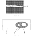
- the metallic material as the present sample therefor there is diffused the Sn or the alloy of Sn 36 as the island shape into the alloy layer of Cu-Sn 35 from the view of cross section as shown in FIG. 12 , and then there becomes to be exposed the part of the Sn or the alloy of Sn 36 as the island shape onto the surface 31 of the alloy layer of Cu-Sn 35. Still further, there is existed the part of the alloy of Cu-Sn at the inside of the Sn or of the alloy of Sn that is exposed on the alloy layer of Cu-Sn as schematically shown in FIG. 16 and in FIG. 17 , that there is exposed such the Sn or the alloy of Sn as approximately looked like a doughnut shape from a point of view of the surface thereof.
- the number 4 in accordance with FIG. 16 and with FIG. 17 designates a metal layer of Cu-Sn by plating on the most surface thereof
- the number 4b therein designates an intermetallic compound of Cu-Sn
- the number 4c therein designates a part of the Sn or the alloy of Sn by which there is formed the layer of Sn (the S-layer) in accordance with FIG. 2 .
- such the intermetallic compound of Cu-Sn 4b therein becomes to form a part of the layer of the most surface thereof by being combined with the alloy layer of Cu-Sn 4.
- a thickness of the intermediate layer 3 in the metallic material for the connector 5 there is no limitation in particular regarding a thickness of the intermediate layer 3 in the metallic material for the connector 5.
- a thickness of the alloy layer of Cu-Sn 4 in the metallic material for the connector 5 in accordance with the present invention it is desirable therefor to be as between 0.05 ⁇ m and 2.0 ⁇ m, or it is further preferable therefor to be as between 0.1 ⁇ m and 1.0 ⁇ m.
- the intermediate layer 3 which is comprised of copper or the alloy of copper in such the metallic material for the connector 5 in accordance with the present invention. And then there is seldom worsened such as the properties of inserting thereinto and extracting the terminal thereinto or the like, regarding such the metallic material therein even in a case where there may be assumed for the C-layer 3a to be disappeared therefrom together with the S-layer 4a after performing the process of treating with heat for the above mentioned layered body by plating 6.
- the alloy layer of Cu-Sn by plating as the most surface thereof in accordance with the present invention is desirable for the alloy layer of Cu-Sn by plating as the most surface thereof in accordance with the present invention to be designed as decreasing the concentration of Cu therein as gradually from a side for the substrate toward the surface thereof. And then in such the case thereof there becomes not to be formed clearly a boundary of between such the alloy layer of Cu-Sn and the layer of Cu which is existing under such the alloy layer or a boundary of between such the alloy layer and the substrate.
- the metallic material in accordance with the present invention that comprises the contact member part in the terminal on which there is designed for the most surface thereof to be as the alloy layer of Cu-Sn with decreasing gradually the concentration of the Cu therein toward the surface thereof and that comprises a joint part for electric wire by pressing to be as the layer of Sn.
- a substantial temperature of the layered body by plating 6 is desirable for a substantial temperature of the layered body by plating 6 to be as between 232 °C and 500 °C, with an amount of time for between 0.1 second and ten minutes, or therewith for not longer than 100 seconds as it is more desirable therefor, or therewith for not longer than ten seconds as it is further preferable therefor.
- the above mentioned layered body in a case of performing such the process thereof by making use of a batch processing therefor, it is desirable for the above mentioned layered body to be performed by being maintained in a furnace which has a temperature of between 50 °C and 250 °C, with an amount of time for between several tens minutes and several hours. Furthermore, there are required for such as the temperature thereof or the amount of time for heating thereof or the like in the case of performing the process of treating with heat therefor by making use of the reflow treatment therefor to be set as a condition that is pursuant to such as each of the thicknesses of the N-layer 2a and the C-layer 3a and the S-layer 4a in the layered body by plating 6 or the like. And then it is able to set each of the specific conditions thereof as properly, that will be described in detail later in accordance with the following Examples.
- the electrically conductive substrate 1 to be made use as properly of such as copper, an alloy of copper, such as aphosphor bronze, a brass, a white metal, a beryllium copper, a Corson alloy, or the like, iron, an alloy of iron, such as a stainless steel or the like, a composite material, such as a material of iron to be covered by copper, a material of iron to be covered by nickel, or the like, an alloy of nickel as a variety thereof, an alloy of aluminum as a variety thereof, or the like, that each of such the materials individually have the electrical conductivities and the mechanical strengths and the heat resisting properties that are required for the terminal respectively.
- an alloy of copper such as aphosphor bronze, a brass, a white metal, a beryllium copper, a Corson alloy, or the like
- iron, an alloy of iron, such as a stainless steel or the like a composite material, such as a material of iron to be covered by copper, a material of iron to be covered by nickel, or the like,
- the copper based material in particular of such as copper or the copper alloy or the like among the above mentioned metal and the alloys (materials), as it is superior in a balance of between the electrical conductivity thereof and the mechanical strength thereof.
- the copper based material in particular of such as copper or the copper alloy or the like among the above mentioned metal and the alloys (materials), it is superior in a balance of between the electrical conductivity thereof and the mechanical strength thereof.
- the electrically conductive substrate 1 in a case where there is designed for the above mentioned electrically conductive substrate 1 to be made use of the other material except such the copper based material, it becomes able to improve a corrosion resistance thereof and an adherence to between the underlayer 2 by being covered a surface thereof with making use of copper or an alloy of copper.
- the underlayer 2 to be provided onto the above mentioned electrically conductive substrate 1 there is made use as preferred thereto of such as a metal of Ni or Co or Fe, an alloy of Ni, such as a system of Ni-P, a system of Ni-Sn, a system of Co-P, a system of Ni-Co, a system of Ni-Co-P, a system of Ni-Cu, a system of Ni-Cr, a system of Ni-Zn, a system of Ni-Fe, or the like, an alloy of Fe, an alloy of Co, or the like, that individually have the barrier function to prevent any of the elements in the substrate from the occurrence of the thermal diffusion into the alloy layer of Cu-Sn 4.
- an alloy of Ni such as a system of Ni-P, a system of Ni-Sn, a system of Co-P, a system of Ni-Co, a system of Ni-Co-P, a system of Ni-Cu, a system of Ni-Cr, a system of Ni-Zn, a system
- such the metal (alloy) of such as Ni or the like to be made use for the above mentioned underlayer 2 has a melting point as high as not lower than 1000 °C. While, a temperature of an environment for a usage of a connector to be connected is normally lower on the contrary thereto as not higher than 200 °C. And then thereby it is difficult for such the underlayer 2 to be occurred the thermal diffusion of itself. And hence it becomes able to come out the barrier function thereof as effectively. Still further, such the underlayer 2 has a further function to enhance an adherence of between the electrically conductive substrate 1 and the intermediate layer 3 with corresponding to the material to be made use for such the electrically conductive substrate 1.
- a thickness of such the underlayer 2 it becomes not able to function such the barrier function as sufficiently in a case where it is thinner than 0.05 ⁇ m. While, there becomes to be larger a distortion due to the plating thereon in a case where it is thicker than 3 ⁇ m on the contrary thereto. And then thereby there becomes to be peeled off as easier such the layer from the substrate. And hence it is desirable therefor to be as between 0.05 ⁇ m and 3 ⁇ m. Still further, it is more desirable for an upper limit regarding such the thickness of the underlayer 2 to be as not thicker than 1.5 ⁇ m, or it is further preferable therefor to be as not thicker than 0.5 ⁇ m, with taking into consideration of workability on the terminal.
- the underlayer 2 may be available to design such the underlayer 2 as one layer or layers as not less than two thereof. Furthermore, in a case where there is designed therefor to be the layers as not less than two thereof, it becomes able to obtain a further advantage of such as being able to set as properly such as the barrier function or the function to enhance the adherence to therebetween or the like, due to a relation to between the other layer as adjacent thereto.
- an alloy of copper such as a system of Cu-Sn or the like, in addition to copper as preferred to the intermediate layer 3 therein. And then it is desirable for a concentration of Cu in such the alloy of copper to be as not lower than fifty mass percent in such the case thereof.
- a volume ratio of between the volume of the S-layer 4a and that of the C-layer 3a that is defined as (S/C) is desirable to be as not higher than 1.85 in a case where the S-layer 4a is comprised of Sn and where the C-layer 3a is comprised of Cu.
- a thickness of the above mentioned S-layer 4a is desirable for a volume ratio of between the volume of the S-layer 4a and that of the C-layer 3a that is defined as (S/C) to be as not higher than 1.85 in a case where the S-layer 4a is comprised of Sn and where the C-layer 3a is comprised of Cu.
- a thickness of the above mentioned S-layer 4a is as not thicker than 9.5 ⁇ m.
- N-layer 2a that is comprised of such as Ni or the like
- C-layer 3a that is comprised of such as Cu or the like
- S-layer 4a that is comprised of such as Sn or the like
- plating 6 by making use of such as a method of a physical vapor deposition (PVD) or the like.
- PVD physical vapor deposition
- an intermetallic compound of Cu-Sn in order to form the alloy layer of Cu-Sn 4, such as a Cu 6 Sn 5 , a Cu 3 Sn, a Cu 4 Sn, or the like.
- the Cu 6 Sn 5 is generated by being reacted Sn as a volume of 1.90 with corresponding to a volume as one for Cu.
- the Cu 3 Sn is generated by being reacted Sn as the volume of 0.76 with corresponding to the volume as one for Cu on the contrary thereto.
- the Cu 4 Sn is generated by being reacted Sn as the volume of 0.57 with corresponding to the volume as one for Cu on the contrary thereto.
- an alloy layer of Cu-Sn in which the Cu 6 Sn 5 is dominant in a case of performing a process of treating with heat for a layered body by plating with an amount of time for longer that has the volume ratio of between the volume of the S-layer 4a and that of the C-layer 3a as the (S/C) to be as between 1.90 and 1.80 for instance.
- another alloy layer of Cu-Sn in which the Cu 3 Sn is dominant in a case of performing the process of treating with heat for another layered body by plating with an amount of time for longer that has the above mentioned ratio of volumes of therebetween to be as between 0.76 and 0.70 on the contrary thereto for instance.
- the alloy layer of Cu-Sn 4 by making use of the layers as two of the layer of Cu 6 Sn 5 and the layer of Cu 3 Sn in accordance with the present invention, there is no specification in particular regarding a thickness of each of such the layers therein.
- the layer of Cu 6 Sn 5 therein it is further preferable for the layer of Cu 6 Sn 5 therein to be as between 0.01 ⁇ m and 5.0 ⁇ m, and it is further preferable for the layer of Cu 3 Sn therein to be as between 0.008 ⁇ m and 4.0 ⁇ m as well.
- the metallic material for the connector 5 in accordance with the present invention there becomes not to be affected negatively onto the performance thereof even in a case where there is formed an oxide film layer which has a thickness of not thicker than 100 nm onto the surface of the alloy layer of Cu-Sn 4.
- the metallic material for the connector 5 in accordance with the present invention there is designed for the outermost layer 4a before performing the process of treating with heat therefor to be as the Sn or the alloy of Sn, and then thereby there becomes to be formed an oxide of Sn as an oxidized substance in the case thereof. And then such the oxide of Sn has an electrical conductivity as higher comparing to that of such as an oxide of Cu or the like. And hence it may be considered that there becomes not to be affected negatively onto the electrical conductivity thereof as the metallic material. Still further, it is desirable for such the thickness of the oxide film layer thereon to be as not thicker than 30 nm.
- a dissimilar material as a different kind therefrom to be interjacent at between the electrically conductive substrate 1 and the underlayer 2, and/or at between the underlayer 2 and the intermediate layer 3, and/or at between the intermediate layer 3 and the alloy layer of Cu-Sn 4, that has a thickness as thinner than that of each of the layers to be adjacent thereto.
- the alloy layer of Cu-Sn 4 may be provided onto the electrically conductive substrate 1 regarding the metallic material in accordance with the present invention, and it may be available to design such the alloy layer of Cu-Sn 4 to be provided onto the underlayer 2 which is provided on the electrically conductive substrate 1 as well.
- a shape of the metallic material for the connector in accordance with the present invention such as a bar material or a plate material or the like, if such the material has a shape that forms at least a part of the male terminal in the connector and/or at least a part of the female terminal therein.
- a connector for another embodiment in accordance with the present invention in which such the above mentioned metallic material for the connector configures at least a contact member part therein. And then it is desirable therefor in particular to be as a connector of a multi way type or as a contact shoe. Moreover, it becomes able to work with making use of the metallic material for the connector in accordance with the present invention into such as a connector or a contact shoe or the like for a usage of such as a motor vehicle or of an electrical device or of an electronic device or the like.
- the connector for an electrical device and for an electronic device that is comprised of the male terminal and the female terminal, that becomes to be easier for the production thereof, that becomes to have the electrical connectability as further stable, and that there becomes to be improved the properties for inserting thereinto and for extracting therefrom, and it becomes available therein to provide the metallic material for a connector as well, that is made use for such the connector, and then that becomes to be applied as preferred to such as the connect member part in the male terminal or in the female terminal or the like.
- the connector which is characterized in that there is designed for such the connector to comprise the male terminal and the female terminal that it is possible to connect to each other, that there is designed for all over the surface of the terminal of either one of the above mentioned male terminal or the above mentioned female terminal or at least the contact member part of either one thereof only to be formed with making use of the metallic material in which the most surface thereof is the alloy layer of Cu-Sn, and that there is designed for all over the surface of the other terminal against the either one of the above mentioned male terminal or the above mentioned female terminal or at least the contact member part of such the other terminal against the either one thereof only to be formed with making use of the metallic material in which the most surface thereof is the layer of Sn or the alloy layer of Sn.
- the volume ratio of between the volume of the S-layer and that of the C-layer as the (S/C) is designed for the volume ratio of between the volume of the S-layer and that of the C-layer as the (S/C) to be varied in a variety thereof regarding the layered body by plating to be produced thereby. And then thereafter there is performed a process of treating with heat for such the layered body by plating, and hence there is produced the following individual samples of the metallic material as the sample numbers of 1 to 3 that individually have the configurations as shown in FIG. 4 and FIG. 6 through FIG. 17 respectively.
- FIG. 4 corresponds to the sample number as 1 of the metallic material
- all of FIG. 6 through FIG. 10 correspond to the sample number as 2 of the metallic material
- all of FIG. 11 through FIG. 17 correspond to the sample number as 3 of the metallic material.
- each of such the metallic materials to be obtained thereby first of all there is performed for each of the samples with the oblique section of thirty degrees by making use of the focused ion beam (FIB) with setting the same to be inclined as sixty degrees, and each of such the samples is assumed to be as the sample for the Auger analysis and measurement (AES). Still further, there is performed such the analysis of the AES with each of such the samples to be inclined for having the oblique section of thirty degrees to become horizontal. And hence there becomes to be obtained each of the individual electron images of the AES, and then by making thereof there is measured a thickness of each of the layers thereon. Furthermore, there is shown a configuration of each of such the samples in the following Table 2.
- a projected part of hemispheric shape 41a which has a radius of curvature as 1.8 mm with being performed a reflow plating of Sn for an outside surface of the projected convex part to have a thickness of approximately 1 ⁇ m on the metallic material 41, and that the metallic material 42 comprises an alloy layer of Cu-Sn 42a.
- a process of cleaning for removing any grease from both of such the materials and then thereafter there is contacted to therebetween with a contact pressure of 3 N.
- a sliding for going and coming back the both of such the materials with a distance for sliding as 30 ⁇ m under an environment at a temperature of 20 °C and with a humidity of 65 % approximately.
- a coefficient of dynamic friction for each thereof by making use of a friction tester of the Bowden type under the following conditions of the load as 2.94 N, the distance of sliding as 10 mm, the velocity of sliding as 100 mm/min and the number of times for sliding as one time.
- a partner material therefor on which there is performed a work for forming a projected part to have a curvature of 0.5 mm R after performing a reflow plating of Sn with a thickness of approximately 1 ⁇ m onto a bar material of brass which has a plate thickness of 0.25 mm approximately.
- Table 3 there is shown both in Table 3 regarding each of the results from such the individual measurements for each of the coefficient of friction.
- a production of a connector that is comprised of the individual male terminals in accordance with the following Comparative example 1 and the following Present invention example 1 to 4, and the individual female terminals that individually are connectable with such the corresponding male terminals respectively, with making use of each of the materials which is performed the process of the reflow treatment under the conditions of treating with heat therefor as shown in the above Table 1 (the temperature thereof and the amount of time therefor), and that are shown in FIG. 1 and in FIG. 2 .
- the surface of the female terminal in accordance with Present invention example 1 and for the surface of the male terminal in accordance with Present invention example 3 to be formed as the alloy of Cu-Sn individually for all over the individual surfaces thereof as shown in FIG. 6 through FIG.
- each of the connectors in accordance with Present invention example 1 through 4 as shown in Table 5 it becomes able to reduce the force for inserting thereinto as not less than 0.1 N as comparing to the connector in accordance with Comparative example 1, and then thereby it becomes able to obtain the property of insertion thereinto and of extraction therefrom as further excellently.
Applications Claiming Priority (2)
| Application Number | Priority Date | Filing Date | Title |
|---|---|---|---|
| JP2007102099 | 2007-04-09 | ||
| PCT/JP2008/056414 WO2008126719A1 (ja) | 2007-04-09 | 2008-03-31 | コネクタおよびコネクタ用金属材料 |
Publications (4)
| Publication Number | Publication Date |
|---|---|
| EP2157668A1 true EP2157668A1 (de) | 2010-02-24 |
| EP2157668A4 EP2157668A4 (de) | 2012-07-18 |
| EP2157668B1 EP2157668B1 (de) | 2015-11-11 |
| EP2157668B9 EP2157668B9 (de) | 2016-02-17 |
Family
ID=39863824
Family Applications (1)
| Application Number | Title | Priority Date | Filing Date |
|---|---|---|---|
| EP08739527.3A Not-in-force EP2157668B9 (de) | 2007-04-09 | 2008-03-31 | Verbinder und metallmaterial für einen verbinder |
Country Status (5)
| Country | Link |
|---|---|
| US (1) | US8342895B2 (de) |
| EP (1) | EP2157668B9 (de) |
| JP (1) | JP5192878B2 (de) |
| CN (1) | CN101682135B (de) |
| WO (1) | WO2008126719A1 (de) |
Cited By (4)
| Publication number | Priority date | Publication date | Assignee | Title |
|---|---|---|---|---|
| EP2169093A1 (de) * | 2007-05-29 | 2010-03-31 | The Furukawa Electric Co., Ltd. | Metallmaterial für elektrische elektronikbauteile |
| CN102237593A (zh) * | 2010-03-25 | 2011-11-09 | Wago管理有限责任公司 | 导线引入插头 |
| EP2590268A1 (de) * | 2011-11-02 | 2013-05-08 | Sumitomo Wiring Systems, Ltd. | Buchsenanschlussstück und Verfahren zu dessen Herstellung |
| EP4220865A1 (de) * | 2020-02-07 | 2023-08-02 | Northrop Grumman Systems Corporation | Selbstisolierender kontakt für einen nasselektroverbinder |
Families Citing this family (33)
| Publication number | Priority date | Publication date | Assignee | Title |
|---|---|---|---|---|
| EP2273621A4 (de) * | 2008-03-19 | 2011-07-13 | Furukawa Electric Co Ltd | Anschluss für einen verbinder und prozess zum herstellen des anschlusses für einen verbinder |
| JP2010267418A (ja) * | 2009-05-12 | 2010-11-25 | Furukawa Electric Co Ltd:The | コネクタ |
| JP5325734B2 (ja) * | 2009-08-18 | 2013-10-23 | 三菱伸銅株式会社 | 導電部材及びその製造方法 |
| JP5442385B2 (ja) * | 2009-10-07 | 2014-03-12 | 三菱伸銅株式会社 | 導電部材及びその製造方法 |
| JP5036892B2 (ja) * | 2010-05-10 | 2012-09-26 | 株式会社神戸製鋼所 | コンタクトプローブ |
| JP5714863B2 (ja) * | 2010-10-14 | 2015-05-07 | 矢崎総業株式会社 | 雌端子および雌端子の製造方法 |
| JP6029435B2 (ja) * | 2012-06-27 | 2016-11-24 | Jx金属株式会社 | 電子部品用金属材料及びその製造方法、それを用いたコネクタ端子、コネクタ及び電子部品 |
| JP5427945B2 (ja) * | 2012-06-27 | 2014-02-26 | Jx日鉱日石金属株式会社 | 電子部品用金属材料及びその製造方法、それを用いたコネクタ端子、コネクタ及び電子部品 |
| JP6050664B2 (ja) * | 2012-06-27 | 2016-12-21 | Jx金属株式会社 | 電子部品用金属材料及びその製造方法、それを用いたコネクタ端子、コネクタ及び電子部品 |
| WO2014017238A1 (ja) * | 2012-07-25 | 2014-01-30 | Jx日鉱日石金属株式会社 | 電子部品用金属材料及びその製造方法、それを用いたコネクタ端子、コネクタ及び電子部品 |
| AU2012394374B2 (en) * | 2012-11-08 | 2018-03-15 | Monnaie Royale Canadienne / Royal Canadian Mint | Enhanced techniques for production of golden bronze by inter-diffusion of tin and copper under controlled conditions |
| KR101515772B1 (ko) * | 2013-02-24 | 2015-04-28 | 후루카와 덴키 고교 가부시키가이샤 | 금속 부재, 단자, 전선 접속 구조체, 및 단자의 제조 방법 |
| US9054435B2 (en) * | 2013-07-18 | 2015-06-09 | GM Global Technology Operations LLC | Conversion terminal device and method for coupling dissimilar metal electrical components |
| WO2015083547A1 (ja) * | 2013-12-04 | 2015-06-11 | 株式会社オートネットワーク技術研究所 | 電気接点およびコネクタ端子対 |
| DE112015001904T5 (de) | 2014-04-24 | 2016-12-29 | Yazaki Corporation | Kontaktverbindungsstruktur |
| JP5883201B1 (ja) * | 2014-09-26 | 2016-03-09 | 京セラ株式会社 | 音響発生器、音響発生装置および電子機器 |
| CN105637898B (zh) | 2014-09-26 | 2019-04-26 | 京瓷株式会社 | 声音产生器、声音产生装置以及电子设备 |
| JP6361477B2 (ja) * | 2014-11-19 | 2018-07-25 | 株式会社オートネットワーク技術研究所 | コネクタ用端子 |
| JP5984980B2 (ja) * | 2015-02-24 | 2016-09-06 | Jx金属株式会社 | 電子部品用Snめっき材 |
| JP5984981B2 (ja) * | 2015-02-24 | 2016-09-06 | Jx金属株式会社 | 電子部品用Snめっき材 |
| JP6204953B2 (ja) * | 2015-09-18 | 2017-09-27 | 矢崎総業株式会社 | 端子付き電線及びそれを用いたワイヤーハーネス |
| JP6423383B2 (ja) * | 2016-03-31 | 2018-11-14 | 日新製鋼株式会社 | 接続部品用材料 |
| WO2018074256A1 (ja) * | 2016-10-17 | 2018-04-26 | 古河電気工業株式会社 | 導電性条材 |
| US9859640B1 (en) | 2016-11-14 | 2018-01-02 | Te Connectivity Corporation | Electrical connector with plated signal contacts |
| US11152729B2 (en) | 2016-11-14 | 2021-10-19 | TE Connectivity Services Gmbh | Electrical connector and electrical connector assembly having a mating array of signal and ground contacts |
| US20190103693A1 (en) * | 2017-09-29 | 2019-04-04 | Apple Inc. | Electrical contacts having sacrificial layer for corrosion protection |
| JP7067766B2 (ja) * | 2017-12-04 | 2022-05-16 | 石原ケミカル株式会社 | Sn層又はSn合金層を含む構造体 |
| JP2020047500A (ja) * | 2018-09-20 | 2020-03-26 | 矢崎総業株式会社 | 端子嵌合構造 |
| JP7111000B2 (ja) * | 2019-01-18 | 2022-08-02 | 株式会社オートネットワーク技術研究所 | 金属材および接続端子 |
| JP2020149805A (ja) * | 2019-03-11 | 2020-09-17 | 株式会社オートネットワーク技術研究所 | 端子、コネクタ、端子対、及びコネクタ対 |
| JP7352851B2 (ja) * | 2019-08-05 | 2023-09-29 | 株式会社オートネットワーク技術研究所 | 電気接点材料、端子金具、コネクタ、及びワイヤーハーネス |
| JP6958643B2 (ja) * | 2020-01-10 | 2021-11-02 | トヨタ自動車株式会社 | 評価方法 |
| CN114094373A (zh) * | 2020-06-22 | 2022-02-25 | 华为技术有限公司 | 导电端子、电连接器和电子设备 |
Citations (6)
| Publication number | Priority date | Publication date | Assignee | Title |
|---|---|---|---|---|
| EP1026287A1 (de) * | 1999-02-03 | 2000-08-09 | Dowa Mining Co., Ltd. | Verfahren zur Herstellung von Kupfer sowie Kupferlegierungen |
| US20030091855A1 (en) * | 2001-01-19 | 2003-05-15 | Hitoshi Tanaka | Plated material, method of producing same, and electrical/electronic part using same |
| US20030186597A1 (en) * | 2002-03-25 | 2003-10-02 | Takeshi Suzuki | Connector terminal |
| JP2004179055A (ja) * | 2002-11-28 | 2004-06-24 | Mitsubishi Shindoh Co Ltd | コネクタ端子、コネクタおよびその製造方法 |
| JP2004339555A (ja) * | 2003-05-14 | 2004-12-02 | Mitsubishi Shindoh Co Ltd | めっき処理材およびその製造方法、コネクタ用端子部材、およびコネクタ |
| JP2006114492A (ja) * | 2004-09-17 | 2006-04-27 | Shinko Leadmikk Kk | プレスフィット用端子及びその製造方法 |
Family Cites Families (19)
| Publication number | Priority date | Publication date | Assignee | Title |
|---|---|---|---|---|
| JP2975246B2 (ja) * | 1993-12-08 | 1999-11-10 | 古河電気工業株式会社 | 電気接点用Snめっき線とその製造方法 |
| US5849424A (en) * | 1996-05-15 | 1998-12-15 | Dowa Mining Co., Ltd. | Hard coated copper alloys, process for production thereof and connector terminals made therefrom |
| JP3286560B2 (ja) * | 1997-04-28 | 2002-05-27 | 株式会社オートネットワーク技術研究所 | 嵌合型接続端子 |
| JPH10302867A (ja) | 1997-04-28 | 1998-11-13 | Harness Sogo Gijutsu Kenkyusho:Kk | 嵌合型接続端子の製造方法 |
| US5967860A (en) * | 1997-05-23 | 1999-10-19 | General Motors Corporation | Electroplated Ag-Ni-C electrical contacts |
| JPH11135226A (ja) * | 1997-10-27 | 1999-05-21 | Harness Syst Tech Res Ltd | 嵌合型接続端子の製造方法 |
| JP3411824B2 (ja) | 1998-06-30 | 2003-06-03 | 株式会社オートネットワーク技術研究所 | 嵌合型接続端子の製造方法 |
| JP3465876B2 (ja) | 1999-01-27 | 2003-11-10 | 同和鉱業株式会社 | 耐摩耗性銅または銅基合金とその製造方法ならびに該耐摩耗性銅または銅基合金からなる電気部品 |
| US6537091B2 (en) * | 2000-11-28 | 2003-03-25 | Autonetworks Technologies, Ltd. | Arc discharge suppressive terminal, method for producing such terminal, and arc discharge suppressive connector |
| JP4090302B2 (ja) | 2001-07-31 | 2008-05-28 | 株式会社神戸製鋼所 | 接続部品成形加工用導電材料板 |
| JP4753502B2 (ja) | 2001-09-11 | 2011-08-24 | 株式会社神戸製鋼所 | 錫−銅金属間化合物分散錫めっき端子 |
| JP4247339B2 (ja) | 2002-01-21 | 2009-04-02 | Dowaメタルテック株式会社 | Sn被覆部材およびその製造方法 |
| JP4560642B2 (ja) * | 2004-04-19 | 2010-10-13 | Dowaメタルテック株式会社 | Sn被覆導電材の製造方法 |
| JP2005344188A (ja) * | 2004-06-04 | 2005-12-15 | Furukawa Electric Co Ltd:The | めっき材料の製造方法、そのめっき材料を用いた電気・電子部品 |
| JP4292122B2 (ja) * | 2004-07-30 | 2009-07-08 | タイコエレクトロニクスアンプ株式会社 | 電気コネクタ |
| JP2006324063A (ja) * | 2005-05-17 | 2006-11-30 | Ykk Corp | 導電性接続用コネクタ |
| JP4934456B2 (ja) * | 2006-02-20 | 2012-05-16 | 古河電気工業株式会社 | めっき材料および前記めっき材料が用いられた電気電子部品 |
| JP5355935B2 (ja) * | 2007-05-29 | 2013-11-27 | 古河電気工業株式会社 | 電気電子部品用金属材料 |
| EP2173012B1 (de) * | 2007-06-29 | 2019-04-17 | The Furukawa Electric Co., Ltd. | Reibverschleissbeständiger verbinder und verfahren zu seiner herstellung |
-
2008
- 2008-03-31 WO PCT/JP2008/056414 patent/WO2008126719A1/ja active Application Filing
- 2008-03-31 US US12/595,057 patent/US8342895B2/en active Active
- 2008-03-31 CN CN2008800194851A patent/CN101682135B/zh active Active
- 2008-03-31 JP JP2008090606A patent/JP5192878B2/ja active Active
- 2008-03-31 EP EP08739527.3A patent/EP2157668B9/de not_active Not-in-force
Patent Citations (6)
| Publication number | Priority date | Publication date | Assignee | Title |
|---|---|---|---|---|
| EP1026287A1 (de) * | 1999-02-03 | 2000-08-09 | Dowa Mining Co., Ltd. | Verfahren zur Herstellung von Kupfer sowie Kupferlegierungen |
| US20030091855A1 (en) * | 2001-01-19 | 2003-05-15 | Hitoshi Tanaka | Plated material, method of producing same, and electrical/electronic part using same |
| US20030186597A1 (en) * | 2002-03-25 | 2003-10-02 | Takeshi Suzuki | Connector terminal |
| JP2004179055A (ja) * | 2002-11-28 | 2004-06-24 | Mitsubishi Shindoh Co Ltd | コネクタ端子、コネクタおよびその製造方法 |
| JP2004339555A (ja) * | 2003-05-14 | 2004-12-02 | Mitsubishi Shindoh Co Ltd | めっき処理材およびその製造方法、コネクタ用端子部材、およびコネクタ |
| JP2006114492A (ja) * | 2004-09-17 | 2006-04-27 | Shinko Leadmikk Kk | プレスフィット用端子及びその製造方法 |
Non-Patent Citations (1)
| Title |
|---|
| See also references of WO2008126719A1 * |
Cited By (8)
| Publication number | Priority date | Publication date | Assignee | Title |
|---|---|---|---|---|
| EP2169093A1 (de) * | 2007-05-29 | 2010-03-31 | The Furukawa Electric Co., Ltd. | Metallmaterial für elektrische elektronikbauteile |
| EP2169093A4 (de) * | 2007-05-29 | 2012-01-25 | Furukawa Electric Co Ltd | Metallmaterial für elektrische elektronikbauteile |
| US9263814B2 (en) | 2007-05-29 | 2016-02-16 | Furukawa Electric Co., Ltd. | Metal material for electrical electronic component |
| CN102237593A (zh) * | 2010-03-25 | 2011-11-09 | Wago管理有限责任公司 | 导线引入插头 |
| CN102237593B (zh) * | 2010-03-25 | 2015-07-15 | Wago管理有限责任公司 | 导线引入插头 |
| EP2590268A1 (de) * | 2011-11-02 | 2013-05-08 | Sumitomo Wiring Systems, Ltd. | Buchsenanschlussstück und Verfahren zu dessen Herstellung |
| EP4220865A1 (de) * | 2020-02-07 | 2023-08-02 | Northrop Grumman Systems Corporation | Selbstisolierender kontakt für einen nasselektroverbinder |
| EP4101033A4 (de) * | 2020-02-07 | 2024-02-21 | Northrop Grumman Systems Corp | Einziger selbstisolierender kontakt für nasse elektrische verbinder |
Also Published As
| Publication number | Publication date |
|---|---|
| JP5192878B2 (ja) | 2013-05-08 |
| EP2157668A4 (de) | 2012-07-18 |
| WO2008126719A1 (ja) | 2008-10-23 |
| CN101682135B (zh) | 2013-10-02 |
| US20100190390A1 (en) | 2010-07-29 |
| US8342895B2 (en) | 2013-01-01 |
| EP2157668B1 (de) | 2015-11-11 |
| EP2157668B9 (de) | 2016-02-17 |
| CN101682135A (zh) | 2010-03-24 |
| JP2008282802A (ja) | 2008-11-20 |
Similar Documents
| Publication | Publication Date | Title |
|---|---|---|
| EP2157668B9 (de) | Verbinder und metallmaterial für einen verbinder | |
| EP1995356B1 (de) | Plattierungsmaterial und elektrisches und elektronisches bauteil unter verwendung des plattierungsmaterials | |
| EP2620275B1 (de) | Verzinntes Kupferlegierungsmaterial für Klemme und Verfahren zur Herstellung davon | |
| CN108352639B (zh) | 镀锡铜端子材及端子以及电线末端部结构 | |
| JP5355935B2 (ja) | 電気電子部品用金属材料 | |
| EP1352993B1 (de) | Herstellung eines metallplattierten materials | |
| EP1281789B1 (de) | Plattierte Kupferlegierung und Verfahren zu ihre Herstellung | |
| EP2351875B1 (de) | Leitfähiges element und herstellungsverfahren dafür | |
| JP4653133B2 (ja) | めっき材料および前記めっき材料が用いられた電気電子部品 | |
| EP2896724B1 (de) | Verzinntes Klemmenmaterial aus Kupferlegierung | |
| EP3456871B1 (de) | Verzinntes kupferklemmenmaterial, klemme und elektrische drahtendteilstruktur | |
| EP2267187A1 (de) | Metallwerkstoff für anschlussteil und herstellungsverfahren dafür | |
| EP2703524A2 (de) | Sn-beschichtetes Kupferlegierungsband mit ausgezeichneter Wärmebeständigkeit | |
| EP1788585A1 (de) | Leitfähiges material zur teileverbindung und verfahren zur herstellung des leitfähigen materials | |
| EP2173012A1 (de) | Reibverschleissbeständiger verbinder und verfahren zu seiner herstellung | |
| EP2843086A2 (de) | Verzinntes Kupferlegierungsmaterial für einen Anschluss mit hervorragenden Einsetz-/Extraktionseigenschaften | |
| CN110997985A (zh) | 附银皮膜端子材及附银皮膜端子 | |
| JP2010267418A (ja) | コネクタ | |
| EP3575448A1 (de) | Anschlussmaterial für verbinder, anschluss und elektrische drahtendteilstruktur | |
| CN110326168B (zh) | 防腐蚀端子材料及防腐蚀端子以及电线末端部结构 | |
| JP2010267419A (ja) | コネクタおよびコネクタ用金属材料 | |
| US10804632B2 (en) | Connection terminal and method for producing connection terminal | |
| JP7230570B2 (ja) | コネクタ端子用導電部材及びコネクタ端子 |
Legal Events
| Date | Code | Title | Description |
|---|---|---|---|
| PUAI | Public reference made under article 153(3) epc to a published international application that has entered the european phase |
Free format text: ORIGINAL CODE: 0009012 |
|
| 17P | Request for examination filed |
Effective date: 20091109 |
|
| AK | Designated contracting states |
Kind code of ref document: A1 Designated state(s): AT BE BG CH CY CZ DE DK EE ES FI FR GB GR HR HU IE IS IT LI LT LU LV MC MT NL NO PL PT RO SE SI SK TR |
|
| AX | Request for extension of the european patent |
Extension state: AL BA MK RS |
|
| RAP1 | Party data changed (applicant data changed or rights of an application transferred) |
Owner name: FURUKAWA ELECTRIC CO., LTD. |
|
| DAX | Request for extension of the european patent (deleted) | ||
| A4 | Supplementary search report drawn up and despatched |
Effective date: 20120620 |
|
| RIC1 | Information provided on ipc code assigned before grant |
Ipc: C25D 5/50 20060101ALI20120614BHEP Ipc: C25D 7/00 20060101ALI20120614BHEP Ipc: H01R 13/04 20060101ALN20120614BHEP Ipc: C25D 5/12 20060101ALI20120614BHEP Ipc: H01R 13/03 20060101AFI20120614BHEP Ipc: H01R 13/11 20060101ALN20120614BHEP Ipc: H01R 43/16 20060101ALI20120614BHEP |
|
| GRAP | Despatch of communication of intention to grant a patent |
Free format text: ORIGINAL CODE: EPIDOSNIGR1 |
|
| RIC1 | Information provided on ipc code assigned before grant |
Ipc: C25D 5/12 20060101ALI20150430BHEP Ipc: C25D 7/00 20060101ALI20150430BHEP Ipc: H01R 13/11 20060101ALN20150430BHEP Ipc: C25D 3/38 20060101ALN20150430BHEP Ipc: H01R 13/04 20060101ALN20150430BHEP Ipc: C25D 5/10 20060101ALN20150430BHEP Ipc: H01R 43/16 20060101ALI20150430BHEP Ipc: H01R 13/03 20060101AFI20150430BHEP Ipc: C25D 5/50 20060101ALI20150430BHEP Ipc: C25D 3/30 20060101ALN20150430BHEP |
|
| INTG | Intention to grant announced |
Effective date: 20150529 |
|
| RIN1 | Information on inventor provided before grant (corrected) |
Inventor name: YOSHIDA, KAZUO Inventor name: KITAGAWA, SHUICHI Inventor name: SUSAI, KYOTA Inventor name: UNO, TAKEO |
|
| GRAS | Grant fee paid |
Free format text: ORIGINAL CODE: EPIDOSNIGR3 |
|
| GRAA | (expected) grant |
Free format text: ORIGINAL CODE: 0009210 |
|
| AK | Designated contracting states |
Kind code of ref document: B1 Designated state(s): AT BE BG CH CY CZ DE DK EE ES FI FR GB GR HR HU IE IS IT LI LT LU LV MC MT NL NO PL PT RO SE SI SK TR |
|
| REG | Reference to a national code |
Ref country code: GB Ref legal event code: FG4D |
|
| REG | Reference to a national code |
Ref country code: CH Ref legal event code: EP |
|
| REG | Reference to a national code |
Ref country code: IE Ref legal event code: FG4D |
|
| REG | Reference to a national code |
Ref country code: AT Ref legal event code: REF Ref document number: 760864 Country of ref document: AT Kind code of ref document: T Effective date: 20151215 |
|
| REG | Reference to a national code |
Ref country code: DE Ref legal event code: R096 Ref document number: 602008041122 Country of ref document: DE |
|
| REG | Reference to a national code |
Ref country code: LT Ref legal event code: MG4D |
|
| REG | Reference to a national code |
Ref country code: NL Ref legal event code: MP Effective date: 20160211 |
|
| REG | Reference to a national code |
Ref country code: AT Ref legal event code: MK05 Ref document number: 760864 Country of ref document: AT Kind code of ref document: T Effective date: 20151111 |
|
| PG25 | Lapsed in a contracting state [announced via postgrant information from national office to epo] |
Ref country code: ES Free format text: LAPSE BECAUSE OF FAILURE TO SUBMIT A TRANSLATION OF THE DESCRIPTION OR TO PAY THE FEE WITHIN THE PRESCRIBED TIME-LIMIT Effective date: 20151111 Ref country code: HR Free format text: LAPSE BECAUSE OF FAILURE TO SUBMIT A TRANSLATION OF THE DESCRIPTION OR TO PAY THE FEE WITHIN THE PRESCRIBED TIME-LIMIT Effective date: 20151111 Ref country code: NO Free format text: LAPSE BECAUSE OF FAILURE TO SUBMIT A TRANSLATION OF THE DESCRIPTION OR TO PAY THE FEE WITHIN THE PRESCRIBED TIME-LIMIT Effective date: 20160211 Ref country code: LT Free format text: LAPSE BECAUSE OF FAILURE TO SUBMIT A TRANSLATION OF THE DESCRIPTION OR TO PAY THE FEE WITHIN THE PRESCRIBED TIME-LIMIT Effective date: 20151111 Ref country code: IT Free format text: LAPSE BECAUSE OF FAILURE TO SUBMIT A TRANSLATION OF THE DESCRIPTION OR TO PAY THE FEE WITHIN THE PRESCRIBED TIME-LIMIT Effective date: 20151111 Ref country code: IS Free format text: LAPSE BECAUSE OF FAILURE TO SUBMIT A TRANSLATION OF THE DESCRIPTION OR TO PAY THE FEE WITHIN THE PRESCRIBED TIME-LIMIT Effective date: 20160311 Ref country code: NL Free format text: LAPSE BECAUSE OF FAILURE TO SUBMIT A TRANSLATION OF THE DESCRIPTION OR TO PAY THE FEE WITHIN THE PRESCRIBED TIME-LIMIT Effective date: 20151111 |
|
| PG25 | Lapsed in a contracting state [announced via postgrant information from national office to epo] |
Ref country code: LV Free format text: LAPSE BECAUSE OF FAILURE TO SUBMIT A TRANSLATION OF THE DESCRIPTION OR TO PAY THE FEE WITHIN THE PRESCRIBED TIME-LIMIT Effective date: 20151111 Ref country code: PT Free format text: LAPSE BECAUSE OF FAILURE TO SUBMIT A TRANSLATION OF THE DESCRIPTION OR TO PAY THE FEE WITHIN THE PRESCRIBED TIME-LIMIT Effective date: 20160311 Ref country code: AT Free format text: LAPSE BECAUSE OF FAILURE TO SUBMIT A TRANSLATION OF THE DESCRIPTION OR TO PAY THE FEE WITHIN THE PRESCRIBED TIME-LIMIT Effective date: 20151111 Ref country code: PL Free format text: LAPSE BECAUSE OF FAILURE TO SUBMIT A TRANSLATION OF THE DESCRIPTION OR TO PAY THE FEE WITHIN THE PRESCRIBED TIME-LIMIT Effective date: 20151111 Ref country code: SE Free format text: LAPSE BECAUSE OF FAILURE TO SUBMIT A TRANSLATION OF THE DESCRIPTION OR TO PAY THE FEE WITHIN THE PRESCRIBED TIME-LIMIT Effective date: 20151111 Ref country code: GR Free format text: LAPSE BECAUSE OF FAILURE TO SUBMIT A TRANSLATION OF THE DESCRIPTION OR TO PAY THE FEE WITHIN THE PRESCRIBED TIME-LIMIT Effective date: 20160212 Ref country code: FI Free format text: LAPSE BECAUSE OF FAILURE TO SUBMIT A TRANSLATION OF THE DESCRIPTION OR TO PAY THE FEE WITHIN THE PRESCRIBED TIME-LIMIT Effective date: 20151111 |
|
| PG25 | Lapsed in a contracting state [announced via postgrant information from national office to epo] |
Ref country code: CZ Free format text: LAPSE BECAUSE OF FAILURE TO SUBMIT A TRANSLATION OF THE DESCRIPTION OR TO PAY THE FEE WITHIN THE PRESCRIBED TIME-LIMIT Effective date: 20151111 |
|
| REG | Reference to a national code |
Ref country code: DE Ref legal event code: R097 Ref document number: 602008041122 Country of ref document: DE |
|
| PG25 | Lapsed in a contracting state [announced via postgrant information from national office to epo] |
Ref country code: BE Free format text: LAPSE BECAUSE OF NON-PAYMENT OF DUE FEES Effective date: 20160331 Ref country code: DK Free format text: LAPSE BECAUSE OF FAILURE TO SUBMIT A TRANSLATION OF THE DESCRIPTION OR TO PAY THE FEE WITHIN THE PRESCRIBED TIME-LIMIT Effective date: 20151111 Ref country code: RO Free format text: LAPSE BECAUSE OF FAILURE TO SUBMIT A TRANSLATION OF THE DESCRIPTION OR TO PAY THE FEE WITHIN THE PRESCRIBED TIME-LIMIT Effective date: 20151111 Ref country code: EE Free format text: LAPSE BECAUSE OF FAILURE TO SUBMIT A TRANSLATION OF THE DESCRIPTION OR TO PAY THE FEE WITHIN THE PRESCRIBED TIME-LIMIT Effective date: 20151111 Ref country code: SK Free format text: LAPSE BECAUSE OF FAILURE TO SUBMIT A TRANSLATION OF THE DESCRIPTION OR TO PAY THE FEE WITHIN THE PRESCRIBED TIME-LIMIT Effective date: 20151111 |
|
| PLBE | No opposition filed within time limit |
Free format text: ORIGINAL CODE: 0009261 |
|
| STAA | Information on the status of an ep patent application or granted ep patent |
Free format text: STATUS: NO OPPOSITION FILED WITHIN TIME LIMIT |
|
| 26N | No opposition filed |
Effective date: 20160812 |
|
| PG25 | Lapsed in a contracting state [announced via postgrant information from national office to epo] |
Ref country code: LU Free format text: LAPSE BECAUSE OF FAILURE TO SUBMIT A TRANSLATION OF THE DESCRIPTION OR TO PAY THE FEE WITHIN THE PRESCRIBED TIME-LIMIT Effective date: 20160331 Ref country code: MC Free format text: LAPSE BECAUSE OF FAILURE TO SUBMIT A TRANSLATION OF THE DESCRIPTION OR TO PAY THE FEE WITHIN THE PRESCRIBED TIME-LIMIT Effective date: 20151111 |
|
| REG | Reference to a national code |
Ref country code: CH Ref legal event code: PL |
|
| GBPC | Gb: european patent ceased through non-payment of renewal fee |
Effective date: 20160331 |
|
| PG25 | Lapsed in a contracting state [announced via postgrant information from national office to epo] |
Ref country code: SI Free format text: LAPSE BECAUSE OF FAILURE TO SUBMIT A TRANSLATION OF THE DESCRIPTION OR TO PAY THE FEE WITHIN THE PRESCRIBED TIME-LIMIT Effective date: 20151111 |
|
| REG | Reference to a national code |
Ref country code: IE Ref legal event code: MM4A |
|
| PG25 | Lapsed in a contracting state [announced via postgrant information from national office to epo] |
Ref country code: BE Free format text: LAPSE BECAUSE OF FAILURE TO SUBMIT A TRANSLATION OF THE DESCRIPTION OR TO PAY THE FEE WITHIN THE PRESCRIBED TIME-LIMIT Effective date: 20151111 |
|
| REG | Reference to a national code |
Ref country code: FR Ref legal event code: ST Effective date: 20161130 |
|
| PG25 | Lapsed in a contracting state [announced via postgrant information from national office to epo] |
Ref country code: FR Free format text: LAPSE BECAUSE OF NON-PAYMENT OF DUE FEES Effective date: 20160331 Ref country code: CH Free format text: LAPSE BECAUSE OF NON-PAYMENT OF DUE FEES Effective date: 20160331 Ref country code: LI Free format text: LAPSE BECAUSE OF NON-PAYMENT OF DUE FEES Effective date: 20160331 Ref country code: IE Free format text: LAPSE BECAUSE OF NON-PAYMENT OF DUE FEES Effective date: 20160331 Ref country code: GB Free format text: LAPSE BECAUSE OF NON-PAYMENT OF DUE FEES Effective date: 20160331 |
|
| PGFP | Annual fee paid to national office [announced via postgrant information from national office to epo] |
Ref country code: DE Payment date: 20170329 Year of fee payment: 10 |
|
| PG25 | Lapsed in a contracting state [announced via postgrant information from national office to epo] |
Ref country code: MT Free format text: LAPSE BECAUSE OF FAILURE TO SUBMIT A TRANSLATION OF THE DESCRIPTION OR TO PAY THE FEE WITHIN THE PRESCRIBED TIME-LIMIT Effective date: 20151111 |
|
| PG25 | Lapsed in a contracting state [announced via postgrant information from national office to epo] |
Ref country code: HU Free format text: LAPSE BECAUSE OF FAILURE TO SUBMIT A TRANSLATION OF THE DESCRIPTION OR TO PAY THE FEE WITHIN THE PRESCRIBED TIME-LIMIT; INVALID AB INITIO Effective date: 20080331 Ref country code: CY Free format text: LAPSE BECAUSE OF FAILURE TO SUBMIT A TRANSLATION OF THE DESCRIPTION OR TO PAY THE FEE WITHIN THE PRESCRIBED TIME-LIMIT Effective date: 20151111 |
|
| PG25 | Lapsed in a contracting state [announced via postgrant information from national office to epo] |
Ref country code: TR Free format text: LAPSE BECAUSE OF FAILURE TO SUBMIT A TRANSLATION OF THE DESCRIPTION OR TO PAY THE FEE WITHIN THE PRESCRIBED TIME-LIMIT Effective date: 20151111 |
|
| PG25 | Lapsed in a contracting state [announced via postgrant information from national office to epo] |
Ref country code: BG Free format text: LAPSE BECAUSE OF FAILURE TO SUBMIT A TRANSLATION OF THE DESCRIPTION OR TO PAY THE FEE WITHIN THE PRESCRIBED TIME-LIMIT Effective date: 20151111 |
|
| REG | Reference to a national code |
Ref country code: DE Ref legal event code: R119 Ref document number: 602008041122 Country of ref document: DE |
|
| PG25 | Lapsed in a contracting state [announced via postgrant information from national office to epo] |
Ref country code: DE Free format text: LAPSE BECAUSE OF NON-PAYMENT OF DUE FEES Effective date: 20181002 |