EP2126632B1 - Imprint method, chip production process, and imprint apparatus - Google Patents
Imprint method, chip production process, and imprint apparatus Download PDFInfo
- Publication number
- EP2126632B1 EP2126632B1 EP08738738.7A EP08738738A EP2126632B1 EP 2126632 B1 EP2126632 B1 EP 2126632B1 EP 08738738 A EP08738738 A EP 08738738A EP 2126632 B1 EP2126632 B1 EP 2126632B1
- Authority
- EP
- European Patent Office
- Prior art keywords
- resin material
- mold
- electromagnetic wave
- substrate
- imprint
- Prior art date
- Legal status (The legal status is an assumption and is not a legal conclusion. Google has not performed a legal analysis and makes no representation as to the accuracy of the status listed.)
- Not-in-force
Links
- 238000000034 method Methods 0.000 title claims description 27
- 238000004519 manufacturing process Methods 0.000 title claims description 10
- 239000000463 material Substances 0.000 claims description 130
- 229920005989 resin Polymers 0.000 claims description 125
- 239000011347 resin Substances 0.000 claims description 125
- 239000000758 substrate Substances 0.000 claims description 68
- 238000001723 curing Methods 0.000 claims description 22
- 230000007246 mechanism Effects 0.000 claims description 14
- 238000000016 photochemical curing Methods 0.000 claims description 12
- 230000001678 irradiating effect Effects 0.000 claims description 9
- 239000011261 inert gas Substances 0.000 claims description 8
- IJGRMHOSHXDMSA-UHFFFAOYSA-N Atomic nitrogen Chemical compound N#N IJGRMHOSHXDMSA-UHFFFAOYSA-N 0.000 description 12
- XKRFYHLGVUSROY-UHFFFAOYSA-N Argon Chemical compound [Ar] XKRFYHLGVUSROY-UHFFFAOYSA-N 0.000 description 10
- 238000005516 engineering process Methods 0.000 description 8
- 238000001514 detection method Methods 0.000 description 7
- 229910052786 argon Inorganic materials 0.000 description 5
- QVGXLLKOCUKJST-UHFFFAOYSA-N atomic oxygen Chemical compound [O] QVGXLLKOCUKJST-UHFFFAOYSA-N 0.000 description 5
- 229910052757 nitrogen Inorganic materials 0.000 description 5
- 239000001301 oxygen Substances 0.000 description 5
- 229910052760 oxygen Inorganic materials 0.000 description 5
- 230000015556 catabolic process Effects 0.000 description 4
- 238000011109 contamination Methods 0.000 description 4
- 239000000428 dust Substances 0.000 description 4
- PQXKHYXIUOZZFA-UHFFFAOYSA-M lithium fluoride Chemical compound [Li+].[F-] PQXKHYXIUOZZFA-UHFFFAOYSA-M 0.000 description 4
- 230000003287 optical effect Effects 0.000 description 4
- 239000004065 semiconductor Substances 0.000 description 4
- VYPSYNLAJGMNEJ-UHFFFAOYSA-N silicon dioxide Inorganic materials O=[Si]=O VYPSYNLAJGMNEJ-UHFFFAOYSA-N 0.000 description 4
- YZCKVEUIGOORGS-OUBTZVSYSA-N Deuterium Chemical compound [2H] YZCKVEUIGOORGS-OUBTZVSYSA-N 0.000 description 3
- 230000007547 defect Effects 0.000 description 3
- 229910052805 deuterium Inorganic materials 0.000 description 3
- ORUIBWPALBXDOA-UHFFFAOYSA-L magnesium fluoride Chemical compound [F-].[F-].[Mg+2] ORUIBWPALBXDOA-UHFFFAOYSA-L 0.000 description 3
- 229910001635 magnesium fluoride Inorganic materials 0.000 description 3
- QSHDDOUJBYECFT-UHFFFAOYSA-N mercury Chemical compound [Hg] QSHDDOUJBYECFT-UHFFFAOYSA-N 0.000 description 3
- 229910052753 mercury Inorganic materials 0.000 description 3
- 238000001179 sorption measurement Methods 0.000 description 3
- 238000000018 DNA microarray Methods 0.000 description 2
- MYMOFIZGZYHOMD-UHFFFAOYSA-N Dioxygen Chemical compound O=O MYMOFIZGZYHOMD-UHFFFAOYSA-N 0.000 description 2
- YCKRFDGAMUMZLT-UHFFFAOYSA-N Fluorine atom Chemical compound [F] YCKRFDGAMUMZLT-UHFFFAOYSA-N 0.000 description 2
- 239000006087 Silane Coupling Agent Substances 0.000 description 2
- ISQINHMJILFLAQ-UHFFFAOYSA-N argon hydrofluoride Chemical compound F.[Ar] ISQINHMJILFLAQ-UHFFFAOYSA-N 0.000 description 2
- 230000005540 biological transmission Effects 0.000 description 2
- WUKWITHWXAAZEY-UHFFFAOYSA-L calcium difluoride Chemical compound [F-].[F-].[Ca+2] WUKWITHWXAAZEY-UHFFFAOYSA-L 0.000 description 2
- 229910001873 dinitrogen Inorganic materials 0.000 description 2
- 229910001882 dioxygen Inorganic materials 0.000 description 2
- 230000000694 effects Effects 0.000 description 2
- 238000005530 etching Methods 0.000 description 2
- 239000010408 film Substances 0.000 description 2
- 229910052731 fluorine Inorganic materials 0.000 description 2
- 239000011737 fluorine Substances 0.000 description 2
- 239000010436 fluorite Substances 0.000 description 2
- 239000007789 gas Substances 0.000 description 2
- 238000001746 injection moulding Methods 0.000 description 2
- 238000004886 process control Methods 0.000 description 2
- 239000010453 quartz Substances 0.000 description 2
- 229910052594 sapphire Inorganic materials 0.000 description 2
- 239000010980 sapphire Substances 0.000 description 2
- 238000000926 separation method Methods 0.000 description 2
- 229920005992 thermoplastic resin Polymers 0.000 description 2
- 229920001187 thermosetting polymer Polymers 0.000 description 2
- 229910052724 xenon Inorganic materials 0.000 description 2
- FHNFHKCVQCLJFQ-UHFFFAOYSA-N xenon atom Chemical compound [Xe] FHNFHKCVQCLJFQ-UHFFFAOYSA-N 0.000 description 2
- 239000012080 ambient air Substances 0.000 description 1
- 238000004458 analytical method Methods 0.000 description 1
- 230000015572 biosynthetic process Effects 0.000 description 1
- 238000006243 chemical reaction Methods 0.000 description 1
- 239000011248 coating agent Substances 0.000 description 1
- 238000000576 coating method Methods 0.000 description 1
- 229910052681 coesite Inorganic materials 0.000 description 1
- 229910052906 cristobalite Inorganic materials 0.000 description 1
- 230000003247 decreasing effect Effects 0.000 description 1
- 230000002950 deficient Effects 0.000 description 1
- 230000001419 dependent effect Effects 0.000 description 1
- 238000000151 deposition Methods 0.000 description 1
- 230000008021 deposition Effects 0.000 description 1
- 230000006866 deterioration Effects 0.000 description 1
- 230000005611 electricity Effects 0.000 description 1
- 239000001307 helium Substances 0.000 description 1
- 229910052734 helium Inorganic materials 0.000 description 1
- SWQJXJOGLNCZEY-UHFFFAOYSA-N helium atom Chemical compound [He] SWQJXJOGLNCZEY-UHFFFAOYSA-N 0.000 description 1
- 230000006872 improvement Effects 0.000 description 1
- 238000005468 ion implantation Methods 0.000 description 1
- 239000007788 liquid Substances 0.000 description 1
- 239000007769 metal material Substances 0.000 description 1
- 239000006082 mold release agent Substances 0.000 description 1
- 238000000465 moulding Methods 0.000 description 1
- 238000001127 nanoimprint lithography Methods 0.000 description 1
- 239000004038 photonic crystal Substances 0.000 description 1
- 238000003825 pressing Methods 0.000 description 1
- 230000002265 prevention Effects 0.000 description 1
- 230000008569 process Effects 0.000 description 1
- 239000000377 silicon dioxide Substances 0.000 description 1
- 238000004528 spin coating Methods 0.000 description 1
- 238000005507 spraying Methods 0.000 description 1
- 230000003068 static effect Effects 0.000 description 1
- 229910052682 stishovite Inorganic materials 0.000 description 1
- 239000010409 thin film Substances 0.000 description 1
- 239000012780 transparent material Substances 0.000 description 1
- 229910052905 tridymite Inorganic materials 0.000 description 1
- 230000004304 visual acuity Effects 0.000 description 1
Images
Classifications
-
- B—PERFORMING OPERATIONS; TRANSPORTING
- B29—WORKING OF PLASTICS; WORKING OF SUBSTANCES IN A PLASTIC STATE IN GENERAL
- B29C—SHAPING OR JOINING OF PLASTICS; SHAPING OF MATERIAL IN A PLASTIC STATE, NOT OTHERWISE PROVIDED FOR; AFTER-TREATMENT OF THE SHAPED PRODUCTS, e.g. REPAIRING
- B29C37/00—Component parts, details, accessories or auxiliary operations, not covered by group B29C33/00 or B29C35/00
-
- B—PERFORMING OPERATIONS; TRANSPORTING
- B29—WORKING OF PLASTICS; WORKING OF SUBSTANCES IN A PLASTIC STATE IN GENERAL
- B29C—SHAPING OR JOINING OF PLASTICS; SHAPING OF MATERIAL IN A PLASTIC STATE, NOT OTHERWISE PROVIDED FOR; AFTER-TREATMENT OF THE SHAPED PRODUCTS, e.g. REPAIRING
- B29C35/00—Heating, cooling or curing, e.g. crosslinking or vulcanising; Apparatus therefor
- B29C35/02—Heating or curing, e.g. crosslinking or vulcanizing during moulding, e.g. in a mould
- B29C35/08—Heating or curing, e.g. crosslinking or vulcanizing during moulding, e.g. in a mould by wave energy or particle radiation
- B29C35/0888—Heating or curing, e.g. crosslinking or vulcanizing during moulding, e.g. in a mould by wave energy or particle radiation using transparant moulds
-
- B—PERFORMING OPERATIONS; TRANSPORTING
- B29—WORKING OF PLASTICS; WORKING OF SUBSTANCES IN A PLASTIC STATE IN GENERAL
- B29C—SHAPING OR JOINING OF PLASTICS; SHAPING OF MATERIAL IN A PLASTIC STATE, NOT OTHERWISE PROVIDED FOR; AFTER-TREATMENT OF THE SHAPED PRODUCTS, e.g. REPAIRING
- B29C37/00—Component parts, details, accessories or auxiliary operations, not covered by group B29C33/00 or B29C35/00
- B29C37/0053—Moulding articles characterised by the shape of the surface, e.g. ribs, high polish
-
- B—PERFORMING OPERATIONS; TRANSPORTING
- B29—WORKING OF PLASTICS; WORKING OF SUBSTANCES IN A PLASTIC STATE IN GENERAL
- B29C—SHAPING OR JOINING OF PLASTICS; SHAPING OF MATERIAL IN A PLASTIC STATE, NOT OTHERWISE PROVIDED FOR; AFTER-TREATMENT OF THE SHAPED PRODUCTS, e.g. REPAIRING
- B29C43/00—Compression moulding, i.e. applying external pressure to flow the moulding material; Apparatus therefor
- B29C43/003—Compression moulding, i.e. applying external pressure to flow the moulding material; Apparatus therefor characterised by the choice of material
-
- B—PERFORMING OPERATIONS; TRANSPORTING
- B29—WORKING OF PLASTICS; WORKING OF SUBSTANCES IN A PLASTIC STATE IN GENERAL
- B29C—SHAPING OR JOINING OF PLASTICS; SHAPING OF MATERIAL IN A PLASTIC STATE, NOT OTHERWISE PROVIDED FOR; AFTER-TREATMENT OF THE SHAPED PRODUCTS, e.g. REPAIRING
- B29C43/00—Compression moulding, i.e. applying external pressure to flow the moulding material; Apparatus therefor
- B29C43/02—Compression moulding, i.e. applying external pressure to flow the moulding material; Apparatus therefor of articles of definite length, i.e. discrete articles
- B29C43/021—Compression moulding, i.e. applying external pressure to flow the moulding material; Apparatus therefor of articles of definite length, i.e. discrete articles characterised by the shape of the surface
-
- B—PERFORMING OPERATIONS; TRANSPORTING
- B29—WORKING OF PLASTICS; WORKING OF SUBSTANCES IN A PLASTIC STATE IN GENERAL
- B29C—SHAPING OR JOINING OF PLASTICS; SHAPING OF MATERIAL IN A PLASTIC STATE, NOT OTHERWISE PROVIDED FOR; AFTER-TREATMENT OF THE SHAPED PRODUCTS, e.g. REPAIRING
- B29C45/00—Injection moulding, i.e. forcing the required volume of moulding material through a nozzle into a closed mould; Apparatus therefor
-
- B—PERFORMING OPERATIONS; TRANSPORTING
- B82—NANOTECHNOLOGY
- B82Y—SPECIFIC USES OR APPLICATIONS OF NANOSTRUCTURES; MEASUREMENT OR ANALYSIS OF NANOSTRUCTURES; MANUFACTURE OR TREATMENT OF NANOSTRUCTURES
- B82Y10/00—Nanotechnology for information processing, storage or transmission, e.g. quantum computing or single electron logic
-
- B—PERFORMING OPERATIONS; TRANSPORTING
- B82—NANOTECHNOLOGY
- B82Y—SPECIFIC USES OR APPLICATIONS OF NANOSTRUCTURES; MEASUREMENT OR ANALYSIS OF NANOSTRUCTURES; MANUFACTURE OR TREATMENT OF NANOSTRUCTURES
- B82Y40/00—Manufacture or treatment of nanostructures
-
- G—PHYSICS
- G03—PHOTOGRAPHY; CINEMATOGRAPHY; ANALOGOUS TECHNIQUES USING WAVES OTHER THAN OPTICAL WAVES; ELECTROGRAPHY; HOLOGRAPHY
- G03F—PHOTOMECHANICAL PRODUCTION OF TEXTURED OR PATTERNED SURFACES, e.g. FOR PRINTING, FOR PROCESSING OF SEMICONDUCTOR DEVICES; MATERIALS THEREFOR; ORIGINALS THEREFOR; APPARATUS SPECIALLY ADAPTED THEREFOR
- G03F7/00—Photomechanical, e.g. photolithographic, production of textured or patterned surfaces, e.g. printing surfaces; Materials therefor, e.g. comprising photoresists; Apparatus specially adapted therefor
- G03F7/0002—Lithographic processes using patterning methods other than those involving the exposure to radiation, e.g. by stamping
-
- B—PERFORMING OPERATIONS; TRANSPORTING
- B29—WORKING OF PLASTICS; WORKING OF SUBSTANCES IN A PLASTIC STATE IN GENERAL
- B29C—SHAPING OR JOINING OF PLASTICS; SHAPING OF MATERIAL IN A PLASTIC STATE, NOT OTHERWISE PROVIDED FOR; AFTER-TREATMENT OF THE SHAPED PRODUCTS, e.g. REPAIRING
- B29C35/00—Heating, cooling or curing, e.g. crosslinking or vulcanising; Apparatus therefor
- B29C35/02—Heating or curing, e.g. crosslinking or vulcanizing during moulding, e.g. in a mould
- B29C35/08—Heating or curing, e.g. crosslinking or vulcanizing during moulding, e.g. in a mould by wave energy or particle radiation
- B29C35/0805—Heating or curing, e.g. crosslinking or vulcanizing during moulding, e.g. in a mould by wave energy or particle radiation using electromagnetic radiation
- B29C2035/0827—Heating or curing, e.g. crosslinking or vulcanizing during moulding, e.g. in a mould by wave energy or particle radiation using electromagnetic radiation using UV radiation
-
- B—PERFORMING OPERATIONS; TRANSPORTING
- B29—WORKING OF PLASTICS; WORKING OF SUBSTANCES IN A PLASTIC STATE IN GENERAL
- B29C—SHAPING OR JOINING OF PLASTICS; SHAPING OF MATERIAL IN A PLASTIC STATE, NOT OTHERWISE PROVIDED FOR; AFTER-TREATMENT OF THE SHAPED PRODUCTS, e.g. REPAIRING
- B29C43/00—Compression moulding, i.e. applying external pressure to flow the moulding material; Apparatus therefor
- B29C43/02—Compression moulding, i.e. applying external pressure to flow the moulding material; Apparatus therefor of articles of definite length, i.e. discrete articles
- B29C43/021—Compression moulding, i.e. applying external pressure to flow the moulding material; Apparatus therefor of articles of definite length, i.e. discrete articles characterised by the shape of the surface
- B29C2043/023—Compression moulding, i.e. applying external pressure to flow the moulding material; Apparatus therefor of articles of definite length, i.e. discrete articles characterised by the shape of the surface having a plurality of grooves
- B29C2043/025—Compression moulding, i.e. applying external pressure to flow the moulding material; Apparatus therefor of articles of definite length, i.e. discrete articles characterised by the shape of the surface having a plurality of grooves forming a microstructure, i.e. fine patterning
-
- B—PERFORMING OPERATIONS; TRANSPORTING
- B29—WORKING OF PLASTICS; WORKING OF SUBSTANCES IN A PLASTIC STATE IN GENERAL
- B29C—SHAPING OR JOINING OF PLASTICS; SHAPING OF MATERIAL IN A PLASTIC STATE, NOT OTHERWISE PROVIDED FOR; AFTER-TREATMENT OF THE SHAPED PRODUCTS, e.g. REPAIRING
- B29C43/00—Compression moulding, i.e. applying external pressure to flow the moulding material; Apparatus therefor
- B29C43/32—Component parts, details or accessories; Auxiliary operations
- B29C43/36—Moulds for making articles of definite length, i.e. discrete articles
- B29C43/361—Moulds for making articles of definite length, i.e. discrete articles with pressing members independently movable of the parts for opening or closing the mould, e.g. movable pistons
- B29C2043/3615—Forming elements, e.g. mandrels or rams or stampers or pistons or plungers or punching devices
- B29C2043/3634—Forming elements, e.g. mandrels or rams or stampers or pistons or plungers or punching devices having specific surface shape, e.g. grooves, projections, corrugations
-
- B—PERFORMING OPERATIONS; TRANSPORTING
- B29—WORKING OF PLASTICS; WORKING OF SUBSTANCES IN A PLASTIC STATE IN GENERAL
- B29C—SHAPING OR JOINING OF PLASTICS; SHAPING OF MATERIAL IN A PLASTIC STATE, NOT OTHERWISE PROVIDED FOR; AFTER-TREATMENT OF THE SHAPED PRODUCTS, e.g. REPAIRING
- B29C43/00—Compression moulding, i.e. applying external pressure to flow the moulding material; Apparatus therefor
- B29C43/32—Component parts, details or accessories; Auxiliary operations
- B29C43/58—Measuring, controlling or regulating
- B29C2043/5833—Measuring, controlling or regulating movement of moulds or mould parts, e.g. opening or closing, actuating
-
- B—PERFORMING OPERATIONS; TRANSPORTING
- B29—WORKING OF PLASTICS; WORKING OF SUBSTANCES IN A PLASTIC STATE IN GENERAL
- B29C—SHAPING OR JOINING OF PLASTICS; SHAPING OF MATERIAL IN A PLASTIC STATE, NOT OTHERWISE PROVIDED FOR; AFTER-TREATMENT OF THE SHAPED PRODUCTS, e.g. REPAIRING
- B29C43/00—Compression moulding, i.e. applying external pressure to flow the moulding material; Apparatus therefor
- B29C43/32—Component parts, details or accessories; Auxiliary operations
- B29C43/58—Measuring, controlling or regulating
-
- H—ELECTRICITY
- H01—ELECTRIC ELEMENTS
- H01J—ELECTRIC DISCHARGE TUBES OR DISCHARGE LAMPS
- H01J2237/00—Discharge tubes exposing object to beam, e.g. for analysis treatment, etching, imaging
- H01J2237/004—Charge control of objects or beams
- H01J2237/0041—Neutralising arrangements
- H01J2237/0042—Deflection of neutralising particles
-
- H—ELECTRICITY
- H01—ELECTRIC ELEMENTS
- H01J—ELECTRIC DISCHARGE TUBES OR DISCHARGE LAMPS
- H01J2237/00—Discharge tubes exposing object to beam, e.g. for analysis treatment, etching, imaging
- H01J2237/004—Charge control of objects or beams
- H01J2237/0041—Neutralising arrangements
- H01J2237/0044—Neutralising arrangements of objects being observed or treated
- H01J2237/0047—Neutralising arrangements of objects being observed or treated using electromagnetic radiations, e.g. UV, X-rays, light
-
- H—ELECTRICITY
- H01—ELECTRIC ELEMENTS
- H01J—ELECTRIC DISCHARGE TUBES OR DISCHARGE LAMPS
- H01J37/00—Discharge tubes with provision for introducing objects or material to be exposed to the discharge, e.g. for the purpose of examination or processing thereof
- H01J37/02—Details
- H01J37/026—Means for avoiding or neutralising unwanted electrical charges on tube components
Definitions
- the present invention relates to an imprint method and an imprint apparatus.
- the technology is capable of effecting simultaneous processing during formation of a three-dimensional structure on a wafer. For this reason, the technology is expected to be applied to a wide variety of fields as manufacturing technologies and the like for optical devices such as photonic crystal and the like, biochips such as ⁇ -TAS (micro total analysis system), etc.
- optical devices such as photonic crystal and the like, biochips such as ⁇ -TAS (micro total analysis system), etc.
- ⁇ -TAS micro total analysis system
- a layer of a photocurable resin material is formed on a substrate (semiconductor wafer) as a member to be processed constituting the work.
- a mold provided with a fine structure of a desired imprint pattern is aligned with the work and an ultraviolet-curable resin material is filled between the mold and the substrate. Thereafter, the resin material is irradiated with ultraviolet rays to be cured, followed by parting of the mold from the resin material.
- the fine structure of the mold is transferred onto the resin material layer.
- a pattern corresponding to the fine structure of the mold is formed on the substrate.
- Document US 2006249886 A 1 discloses a nanoimprint lithography method of fabricating a nanoadhesive includes steps of (a) preparing a substrate and a mold under the vacuum environment, wherein at least one of the substrate and the mold is transparent, the mold is located over the substrate and has an oppressing portion having nanometer-scale features and a mold release agent located on the surface of the nanometer-scale features; (b) coating a liquid resist cast on the substrate, wherein the resist cast can be hardened by ultraviolet rays; (c) having the mold is pressed on the substrate to enable the resist cast to fill between the nanometer-scale features and the substrate; (d) irradiating the resist cast by the ultraviolet rays for hardening; and (e) releasing the mold from the substrate to enable the resist cast to produce a contrast pattern thereon corresponding to the nanometer-scale features, wherein the resist cast with the contrast pattern is the nanoadhesive.
- Document JP2000218659 A discloses an apparatus and method for injection molding for efficiently eliminating a static electricity generated at an injection molding by spraying an ionized gas to the molding released from a mold.
- a principal object of the present invention is to provide an imprint method capable of alleviating an occurrence of a defect of a transferred pattern caused by discharge breakdown of the transferred pattern or adsorption of dust or contamination to a mold during parting or separation between the mold and a work.
- Another object of the present invention is to provide a chip production process and an imprint apparatus using the imprint method.
- light includes electromagnetic wave of 200nm or less.
- an imprint method as defined in claim 1.
- an imprint apparatus as defined in claim 7.
- a resin material is cured in a state in which an imprint pattern of a mold is in contact or proximity with the resin material on a substrate.
- This state is realized by bringing an uncured resin material and the imprint pattern into direct contact or in proximity with each other.
- the proximity state means a state of indirect contact through, e.g., a parting layer (of a fluorine-containing silane coupling agent or the like).
- the imprint pattern can also be said to be a pattern forming surface (imprint pattern surface).
- the mold will be specifically described later.
- the resin material it is possible to use a photocurable resin material, a thermoplastic resin material, and a thermosetting resin material. With respect to the curing of the resin material, the resin material is not necessarily completely cured.
- the mold is parted (separated) from the cured resin material. Irradiation of an electromagnetic wave for ionizing gaseous molecules in an atmosphere in which the mold and the cured resin material are placed is performed. The parting is effected while irradiating an entire area in which the imprint pattern of the mold is formed and the cured resin material with the electromagnetic wave.
- electrification can occur at the surfaces of the resin material and the mold.
- the electrification can be removed by performing the parting while irradiating the entire area and the resin material with the electromagnetic wave. BY irradiating the entire area with the electromagnetic wave, it is possible to remove the electrification even when the electrification occurs at any portion of the resin material and the mold.
- the irradiation of the cured resin material with the electromagnetic wave may preferably be performed through the mold.
- the irradiation may also be performed through the substrate or from a lateral side with respect to the surfaces of the substrate and the mold.
- transmission of the electromagnetic wave through the mold the removal of electrification can be suitably performed irrespective of a material for the substrate.
- the irradiation of the electromagnetic wave may also be performed in methods other than the method of irradiating the resin material with the electromagnetic wave through the mold.
- the wavelength of the electromagnetic wave may preferably be selected from a range of 100 nm or more and less than 200 nm.
- the electromagnetic wave may preferably be X-rays and may preferably have a wavelength of 0.1 nm or less.
- the electromagnetic wave may also have a wavelength in other ranges so long as they contain the above-described ranges.
- inert gas for the above-described ionization is introduced into an atmosphere in which the mold and the cured resin material are placed.
- a pressure in the atmosphere in which the mold and the resin material are placed is 0.1 Pa or more and 100 Pa or less.
- the irradiation light for curing the resin material may preferably have a wavelength different from a wavelength of the electromagnetic wave for ionizing the gaseous molecules in the atmosphere.
- removal of electrification is performed by introducing inert gas into the atmosphere, in which the mold and the resin material are placed, after the contact between the resin material and the pattern forming surface at which the imprint pattern is formed is performed at a pressure of 0.1 Pa or more and 100 Pa or less in the atmosphere.
- a member including a substrate and a cured resin material layer disposed on the substrate obtained by using the imprint method described in First Embodiment is prepared. Thereafter, the substrate is processed by using the cured resin material as a mask.
- the thus processed substrate can be utilized as a semiconductor chip or a biochip.
- the cured resin material remains as a residual film, the residual film can be removed.
- the processing can be performed by etching or ion implantation.
- the imprint apparatus is an apparatus for imprinting a pattern onto a resin material on a substrate.
- This apparatus includes a mold holding portion for holding a mold having a pattern forming surface at which an imprint pattern is formed, a substrate holding portion for holding the substrate, and an electromagnetic wave generation source for ionizing gaseous molecules in an atmosphere in which the mold held by said mold holding portion is placed.
- the electromagnetic wave generation source is disposed so that the mold is irradiated with an electromagnetic wave generated from the electromagnetic wave so that the electromagnetic wave travels from a surface, of the mold opposite from the pattern forming surface, toward the pattern forming surface.
- the electromagnetic wave generation source may preferably be used for removing electrification generated on the mold and the resin material.
- the electromagnetic wave generated from the electromagnetic wave generation source may preferably have a wavelength selected from a range of 100 nm or more and less than 200 nm.
- Examples of the electromagnetic wave generation source may include an excimer lamp of argon (wavelength in a range with 126 nm as a center), an excimer lamp of argon fluoride (wavelength in a range with 193 nm as a center), an excimer lamp of xenon (wavelength in a range with 172 nm as a center), and a deuterium lamp capable of irradiation with an electromagnetic wave with a wide-range wavelength.
- the electromagnetic wave generation source is not limited thereto.
- the imprint apparatus may preferably be further provided with a resin material curing light source for curing the resin material on the substrate.
- the resin material curing light source may include a high-pressure mercury lamp capable of irradiation with an electromagnetic wave having a wavelength of about 365 nm. It is preferable that the mold is irradiated with the light from the resin material curing light source and the electromagnetic wave from the electromagnetic wave generation source by using an irradiation mechanism common to the light and the electromagnetic wave.
- the resin material may preferably be a photocurable resin material and a light source for photocuring may preferably be used as an irradiation means for curing the resin material. Further, it is preferable that irradiation with the light from the light source for photocuring and the light generated from the electromagnetic wave generation source is performed through the same irradiation mechanism. Further, the light emitted from the irradiation mechanism may preferably have both of a wavelength used for curing the photocurable resin material and a wavelength used for removing the above-described electrification.
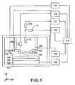
- Figure 1 is a constitutional embodiment of such an imprint apparatus that in order to transfer a pattern of a mold used in this embodiment, a resin material is cured by bringing a pattern forming surface of the mold into contact with the resin material and then the mold is parted from the resin material.
- the imprint apparatus includes a casing 101, a stage 102, a substrate holding portion 103, a substrate 104, a photocurable resin material 105, a mold 106, a mold holding portion 107, a load cell 108, a scope 109, and a light source 110 for photocuring, a light source 111 for electrification removal, a light irradiation mechanism 112, a dispenser 113, a process control circuit 114, an application control circuit 115, a position detection circuit 116, an exposure amount control circuit 117, an electrification removal control circuit 118, a pressure detection circuit 119, and a position control circuit 120.
- the mold 106 and the substrate 104 are disposed opposite to each other.
- the mold 106 is a transparent member having a desired imprint pattern at its surface facing the substrate 104 and is connected to the casing 101 through the mold holding portion 107, the load cell 108, and a member.
- a material for the mold 106 can be appropriately selected from transparent materials capable of transmission of light of a wavelength of 200 nm or less, such as quartz, sapphire, fluorite, magnesium fluoride, lithium fluoride, and the like.
- light with a wavelength of about 150 nm or more is transmissible when quartz or sapphire is used
- light with a wavelength of about 130 nm or more is transmissible when fluorite is used
- light with a wavelength of about 115 nm or more is transmissible when magnesium fluoride is used
- light with a wavelength of about 100 nm or more is transmissible when lithium fluoride is used.
- the mold 106 When the mold 106 is prepared by processing an SiO 2 thin film formed on a magnesium fluoride substrate to form a desired imprint pattern, the mold 106 is excellent in processability and transmissivity of light of a short wavelength (115 nm or more and 150 nm or less in this case).
- a releasing treatment using a fluorine-containing silane coupling agent or the like may generally be performed.
- the light irradiation mechanism 112 is provided as a portion of the casing 101 opposite from a pattern transfer surface of the mold 106.
- Light from the light source 110 for photocuring constituting a means for curing the photocurable resin material and light from the light source 111 for electrification removal constituting an electrification removing means are emitted from the light irradiation mechanism 112.
- the light source 110 for photocuring emits light with a wavelength for curing the photocurable resin material 105.
- the light source 111 for electrification removal emits light from removing electrification of the mold 106, the photocurable resin material 105, and the substrate 104.
- the scope 109 is constituted by a light source, a lens system and a CCD camera and obtains positional information between the mold 106 and the substrate 104.
- the substrate 104 is mounted on the stage 102 through the substrate holding portion 103.
- the stage 102 has six movable directions with respect to 6 axes (x, y, z, ⁇ , ⁇ , ⁇ ) and is secured to the casing 101.
- the dispenser 113 is attached to the casing 101 through a member so that the photocurable resin material 105 can be applied onto the substrate at any position.
- the photocurable resin material 105 is a resin material capable of being cured by irradiation thereof with light of a specific wavelength.
- As the photocurable resin material 105 it is possible to use a resin material ("PAK-01", mfd. by Toyo Gosei Co., Ltd.). This photocurable resin material can be cured by using a high-pressure mercury lamp having a wavelength of about 365 nm.
- the process control circuit 114 provides instructions to the application control circuit 115, the position detection circuit 116, the exposure amount control circuit 117, the electrification removal control circuit 118, the pressure detection circuit 119, and the position control circuit 120 to carry out the imprint process and receive output data from these circuits.
- the application control circuit 115 controls the dispenser 113 so as to apply the photocurable resin material 105 onto the substrate 104.
- the position detection circuit 116 performs image processing of the image obtained by the scope 109 to determine a positional relationship between the mold 106 and the substrate 104.
- the exposure amount control circuit 117 controls the light source 110 for photocuring to perform light exposure.
- the electrification removal control circuit 118 controls the light source 111 for electrification removal to remove electrification from the photocurable resin material 105, the mold 106, and the substrate 104.
- the pressure detection circuit 119 calculates a pressure exerted between the mold 106 and the substrate 104 from a detection signal by the load cell 108 and an area of a portion to be processed.
- the position control circuit 120 controls the stage 102 so that the mold 106 and the substrate 104 can satisfy a desired positional relationship.
- arrangements and methods of the respective mechanisms are not limited to those in this embodiment but may also be applicable to other constitutions. It is possible to employ such a constitution that the electrification removal light source 111 is disposed on a side opposite from the pattern transfer surface of the substrate 104 so that the pattern transfer surface is irradiated with light from the electrification removal light source 111 passing through the substrate 104. It is also possible to employ such a constitution that the photocurable resin material is coated by spin coating in which the mold 106 is moved instead of the substrate 104.
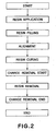
- Figure 2 is a flow chart for illustrating a pattern transfer step in the imprint method in this embodiment.
- the photocurable resin material 105 is applied by the dispenser 113 to prepare a substrate having a resin material-coated surface.
- the mold 106 and the substrate 104 are aligned with each other with a gap, between which the resin material is filled. At this time, a pressing pressure is detected by the load cell 108.
- the substrate 104 onto which the photocurable resin material 105 is applied is disposed opposite to the mold 106 to adjust a positional relationship therebetween by using the scope 109 and the stage 102.
- the resin material filling step corresponds to a contact step for bringing a pattern forming surface (imprint pattern surface), of the mold, for transferring the pattern of the mold onto the resin material on the substrate.
- the resin material between the substrate 104 and the mold 106 is irradiated with light from the photocuring light source 110 to be cured. Thereafter, the irradiation of light from the photocuring light source 110 is stopped.
- an electrification removal (electric charge removal) start step irradiation with light from the electrification removal light source 111 is performed to start the electrification removal from the mold 106, the photocurable resin material 105, and the substrate 104.
- a resin material parting (removal) step the substrate 104 and the mold 106 are moved apart from each other while performing the electrification removal to part (separate) the cured photocurable resin material 105 from the mold 106.
- the electrification removal is completed by stopping the irradiation of light from the electrification removal light source 111.
- the electrification removal start step, the resin material parting step, and the electrification removal end step correspond to a parting step in the present invention for parting the mold from the resin material while performing electrification removal for removing electrification caused during a parting operation when the mold is parted from the resin material cured in the resin material curing step.
- the electrification removal light source 111 continuously emits light from the start of the electrification removal to the end of the electrification removal.
- the imprint pattern at the surface of the mold 106 is transferred onto the resin material layer on the substrate 104.
- the parting is performed while effecting the electrification removal, so that it is possible to improve a throughput.
- the wavelength of the light from the electrification removal light source 111 is selectable from a range of 200 nm or less and may preferably be a range of 100 nm or more and 200 nm or less.
- Example of the electrification removal light source 111 may include an argon excimer lamp (wavelength in a range with 126 nm as a center), an argon fluoride excimer lamp (wavelength in a range with 193 nm as a center), a xenon excimer lamp (wavelength in a range with 172 nm as a center), and a deuterium lamp.
- gaseous molecules in an atmosphere are ionized, so that electrification is removed from the mold 106, the resin material 105, and the substrate 104 in the atmosphere.
- the light with substrate a wavelength is liable to be absorbed by oxygen, so that the electrification removal may suitably be performed in an ionizable atmosphere such as an atmosphere of inert gas such as nitrogen, argon, or the like (low oxygen gas atmosphere) or a reduced-pressure atmosphere.
- an atmosphere of inert gas such as nitrogen, argon, or the like (low oxygen gas atmosphere) or a reduced-pressure atmosphere.
- the electrification removal is performed in a state in which the mold 106 and the substrate 104 are covered with a chamber and the inside of the chamber is aerated with inert gas such as nitrogen, helium, argon, or the like or in a reduced-pressure state.
- the pattern surface of the mold 106 and the neighborhood thereof are placed in an atmosphere with a locally decreased oxygen concentration.
- a nitrogen gas supplying mechanism is provided in the neighborhood of the pattern surface of the mold 106 and nitrogen gas is supplied therefrom during the electrification removal to create an atmosphere with a locally increased nitrogen concentration.
- the electrification removal may be performed in the low oxygen gas atmosphere.
- the photocurable resin material 105 is filled in the gap between the mold 106 and the substrate 104.
- the electrification removal from the mold 106 and the photocurable resin material 105 can be performed while parting the photocurable resin material 105 from the mold 106 in an inert gas atmosphere created by supplying the inert gas such as nitrogen.
- the photocuring light source 110 is selectable from light sources with wavelengths capable of curing the photocurable resin material 105.
- a light source such as the high-pressure mercury lamp is usable.
- the light from the photocurable light source 110 and the light from the electrification removal light source 111 can be configured and positioned to be introduced into the same optical path by using a half mirror to be emitted from the light irradiation mechanism 112.
- the entire transfer pattern surface of the mold 106 is irradiated with the light from the light irradiation mechanism 112.
- the light for the electrification removal is liable to be absorbed by oxygen, so that it is desirable that the optical path from the electrification removal light source 111 to the pattern surface of the mold 106 is placed in the less oxygen atmosphere such as the atmosphere in which the inside of the chamber is aerated with nitrogen or argon or is reduced in pressure.
- the constitutions and arrangements of the photocurable resin material 110 and the electrification removal light source 111 are not limited to those in this embodiment but are applicable to other constitutions. For example, it is possible to employ such a constitution that the light irradiation is performed from separate light irradiation mechanisms.
- the photocurable light source and the electrification removal light source may also be constituted as the same light source with a wavelength for curing the photocurable resin material and a wavelength for performing the electrification removal.
- the light source such as the deuterium lamp having both of the wavelengths for the photocuring and the electrification removal, it is also possible to employ such a constitution that the curing of the photocurable resin material and the electrification removal are performed by the same light source.
- the electromagnetic wave for ionizing the gaseous molecules it is also possible to use X-rays of a wavelength of 0.1 nm or less.
- a mechanism for controlling shielding and irradiation range results in a large scale, so that it is difficult to use the light source and optical system for curing the resin material in common.
- X-rays having good light transmissivity it is possible to effect imprint in not only the less(no) oxygen atmosphere but also the ambient air and to select various members as the mold 106.
- the transfer pattern surface is irradiated through the mold 106 with light with a wavelength of 200 nm or less.
- the ionized gaseous molecules are supplied simultaneously with the parting to remove the electrification from the mold 106, the photocurable resin material 105, and the substrate 104.
- the imprint method and imprint apparatus in this embodiment it is possible to alleviate a degree of occurrence of a defect of the transfer pattern due to discharge breakdown or deposition of dust (contamination) during the parting between the mold 106 and the photocurable resin material 105.
- the photocurable resin material is used as the resin material but other resin materials may also be usable.
- other resin materials may also be usable.
- heat processing is effected by using a thermoplastic resin material or a thermosetting resin material, it is possible to effect similar electrification removal if the mold and the substrate are capable of transmitting therethrough light with a wavelength of 200 nm or less.
- a mold template
- a member to be processed work or resin material
Landscapes
- Engineering & Computer Science (AREA)
- Physics & Mathematics (AREA)
- Chemical & Material Sciences (AREA)
- Nanotechnology (AREA)
- Mechanical Engineering (AREA)
- General Physics & Mathematics (AREA)
- Crystallography & Structural Chemistry (AREA)
- Health & Medical Sciences (AREA)
- Manufacturing & Machinery (AREA)
- Theoretical Computer Science (AREA)
- Toxicology (AREA)
- Oral & Maxillofacial Surgery (AREA)
- Thermal Sciences (AREA)
- Mathematical Physics (AREA)
- Condensed Matter Physics & Semiconductors (AREA)
- Shaping Of Tube Ends By Bending Or Straightening (AREA)
- Exposure Of Semiconductors, Excluding Electron Or Ion Beam Exposure (AREA)
Applications Claiming Priority (2)
| Application Number | Priority Date | Filing Date | Title |
|---|---|---|---|
| JP2007068628 | 2007-03-16 | ||
| PCT/JP2008/055354 WO2008114881A1 (en) | 2007-03-16 | 2008-03-17 | Imprint method, chip production process, and imprint apparatus |
Publications (2)
| Publication Number | Publication Date |
|---|---|
| EP2126632A1 EP2126632A1 (en) | 2009-12-02 |
| EP2126632B1 true EP2126632B1 (en) | 2013-07-03 |
Family
ID=39586034
Family Applications (1)
| Application Number | Title | Priority Date | Filing Date |
|---|---|---|---|
| EP08738738.7A Not-in-force EP2126632B1 (en) | 2007-03-16 | 2008-03-17 | Imprint method, chip production process, and imprint apparatus |
Country Status (6)
| Country | Link |
|---|---|
| US (1) | US8828307B2 (enExample) |
| EP (1) | EP2126632B1 (enExample) |
| JP (1) | JP5137635B2 (enExample) |
| KR (1) | KR101114178B1 (enExample) |
| CN (1) | CN101632040B (enExample) |
| WO (1) | WO2008114881A1 (enExample) |
Families Citing this family (24)
| Publication number | Priority date | Publication date | Assignee | Title |
|---|---|---|---|---|
| US20090166317A1 (en) * | 2007-12-26 | 2009-07-02 | Canon Kabushiki Kaisha | Method of processing substrate by imprinting |
| JP4892025B2 (ja) | 2008-09-26 | 2012-03-07 | 株式会社東芝 | インプリント方法 |
| NL2004685A (en) * | 2009-07-27 | 2011-01-31 | Asml Netherlands Bv | Imprint lithography apparatus and method. |
| JP5583374B2 (ja) * | 2009-09-07 | 2014-09-03 | 株式会社島津製作所 | 光硬化樹脂の特性試験装置、その試験装置で使用する保持具、特性試験方法 |
| KR101134383B1 (ko) | 2009-11-27 | 2012-04-09 | 현대자동차주식회사 | 빛 반사 억제 효과가 우수한 폴리메틸메타크릴레이트 패널 나노임프린팅용 코팅제 |
| JPWO2012020741A1 (ja) * | 2010-08-12 | 2013-10-28 | 株式会社日立ハイテクノロジーズ | 光インプリント方法及び装置 |
| JP5539113B2 (ja) * | 2010-08-30 | 2014-07-02 | キヤノン株式会社 | インプリント装置及び物品の製造方法 |
| JP5836652B2 (ja) | 2011-06-10 | 2015-12-24 | キヤノン株式会社 | インプリント方法、インプリント装置及び物品の製造方法 |
| JP2013003541A (ja) * | 2011-06-21 | 2013-01-07 | Konica Minolta Advanced Layers Inc | 複合レンズの製造方法 |
| JP6200135B2 (ja) | 2012-07-24 | 2017-09-20 | キヤノン株式会社 | インプリント装置、インプリント方法、および、物品製造方法 |
| JP6032036B2 (ja) * | 2013-02-06 | 2016-11-24 | 大日本印刷株式会社 | インプリント方法およびインプリント装置 |
| JP6028602B2 (ja) * | 2013-02-06 | 2016-11-16 | 大日本印刷株式会社 | インプリント方法およびインプリント装置 |
| JP6123321B2 (ja) * | 2013-02-06 | 2017-05-10 | 大日本印刷株式会社 | インプリント方法およびインプリント装置 |
| JP5865340B2 (ja) * | 2013-12-10 | 2016-02-17 | キヤノン株式会社 | インプリント装置及び物品の製造方法 |
| JP6413507B2 (ja) * | 2014-09-02 | 2018-10-31 | 大日本印刷株式会社 | インプリント方法およびインプリント装置 |
| JP6584182B2 (ja) * | 2015-07-16 | 2019-10-02 | キヤノン株式会社 | インプリント装置、インプリント方法および物品製造方法 |
| JP6603678B2 (ja) * | 2016-02-26 | 2019-11-06 | キヤノン株式会社 | インプリント装置およびその動作方法ならびに物品製造方法 |
| WO2017145924A1 (ja) * | 2016-02-26 | 2017-08-31 | キヤノン株式会社 | インプリント装置およびその動作方法ならびに物品製造方法 |
| JP6365619B2 (ja) * | 2016-10-17 | 2018-08-01 | 大日本印刷株式会社 | インプリント方法およびインプリント装置 |
| JP6365620B2 (ja) * | 2016-10-17 | 2018-08-01 | 大日本印刷株式会社 | インプリント方法およびインプリント装置 |
| JP6735656B2 (ja) * | 2016-11-18 | 2020-08-05 | キヤノン株式会社 | インプリント装置、インプリント方法及び物品の製造方法 |
| US11040482B2 (en) * | 2017-02-28 | 2021-06-22 | Toshiba Kikai Kabushiki Kaisha | Transfer method, transfer apparatus, and mold |
| US10895806B2 (en) * | 2017-09-29 | 2021-01-19 | Canon Kabushiki Kaisha | Imprinting method and apparatus |
| JP6948924B2 (ja) * | 2017-11-21 | 2021-10-13 | キヤノン株式会社 | インプリント装置、インプリント方法、および物品製造方法 |
Family Cites Families (25)
| Publication number | Priority date | Publication date | Assignee | Title |
|---|---|---|---|---|
| US4534921A (en) * | 1984-03-06 | 1985-08-13 | Asm Fico Tooling, B.V. | Method and apparatus for mold cleaning by reverse sputtering |
| JPH01101128A (ja) * | 1987-10-15 | 1989-04-19 | Pioneer Electron Corp | 光ディスク製造装置 |
| US5450463A (en) * | 1992-12-25 | 1995-09-12 | Olympus Optical Co., Ltd. | X-ray microscope |
| JPH0745397A (ja) * | 1993-07-27 | 1995-02-14 | Sigma Tec:Kk | 静電気除去装置 |
| JPH10269636A (ja) * | 1997-03-19 | 1998-10-09 | Teijin Ltd | 光記録媒体用基板の製造方法 |
| JP2000218659A (ja) | 1999-01-28 | 2000-08-08 | Sony Corp | 射出成形装置、射出成形方法及びディスク基板 |
| JP2000321777A (ja) * | 1999-05-07 | 2000-11-24 | Toppan Printing Co Ltd | 露光装置 |
| US6504702B1 (en) * | 1999-07-30 | 2003-01-07 | Illinois Tool Works Inc. | Ionizer for static elimination in variable ion mobility environments |
| US6465795B1 (en) * | 2000-03-28 | 2002-10-15 | Applied Materials, Inc. | Charge neutralization of electron beam systems |
| US6729922B2 (en) * | 2000-06-05 | 2004-05-04 | Semiconductor Energy Laboratory Co., Ltd. | Device for inspecting element substrates and method of inspection using this device |
| JP2002353096A (ja) * | 2001-05-22 | 2002-12-06 | Nikon Corp | 基板搬送方法、露光装置及び露光方法 |
| JP3850718B2 (ja) * | 2001-11-22 | 2006-11-29 | 株式会社東芝 | 加工方法 |
| US7122482B2 (en) * | 2003-10-27 | 2006-10-17 | Molecular Imprints, Inc. | Methods for fabricating patterned features utilizing imprint lithography |
| JP5020459B2 (ja) * | 2004-03-29 | 2012-09-05 | 公益財団法人国際科学振興財団 | 樹脂成形機および樹脂成形方法 |
| JP4308739B2 (ja) * | 2004-09-22 | 2009-08-05 | 株式会社フューチャービジョン | 除電装置を備えた射出成形装置 |
| US20060081557A1 (en) * | 2004-10-18 | 2006-04-20 | Molecular Imprints, Inc. | Low-k dielectric functional imprinting materials |
| US7041989B1 (en) * | 2004-10-22 | 2006-05-09 | Asml Netherlands B.V. | Lithographic apparatus and device manufacturing method |
| CN2769065Y (zh) * | 2005-01-31 | 2006-04-05 | 伟诚实业(深圳)有限公司 | 凹印系统的全息印刷装置 |
| JP2006294602A (ja) * | 2005-03-15 | 2006-10-26 | X-Ray Precision Inc | 除電方法、除電装置、ガラス基板の帯電防止方法およびガラス基板の帯電防止装置 |
| JP3971429B2 (ja) | 2005-03-25 | 2007-09-05 | Tdk株式会社 | 光ディスクの製造装置及び製造方法 |
| TWI280159B (en) | 2005-03-29 | 2007-05-01 | Li Bing Huan | Method for fabricating nano-adhesive |
| JP3958344B2 (ja) * | 2005-06-07 | 2007-08-15 | キヤノン株式会社 | インプリント装置、インプリント方法及びチップの製造方法 |
| JP5002211B2 (ja) | 2005-08-12 | 2012-08-15 | キヤノン株式会社 | インプリント装置およびインプリント方法 |
| JP2007098779A (ja) * | 2005-10-05 | 2007-04-19 | Nikon Corp | 樹脂の剥離方法及びパターン転写装置 |
| JP2008098266A (ja) | 2006-10-10 | 2008-04-24 | Canon Inc | 近接場露光装置および近接場露光方法 |
-
2008
- 2008-03-13 JP JP2008064858A patent/JP5137635B2/ja not_active Expired - Fee Related
- 2008-03-17 CN CN2008800079745A patent/CN101632040B/zh not_active Expired - Fee Related
- 2008-03-17 EP EP08738738.7A patent/EP2126632B1/en not_active Not-in-force
- 2008-03-17 WO PCT/JP2008/055354 patent/WO2008114881A1/en not_active Ceased
- 2008-03-17 KR KR1020097021307A patent/KR101114178B1/ko not_active Expired - Fee Related
- 2008-03-17 US US12/091,836 patent/US8828307B2/en not_active Expired - Fee Related
Also Published As
| Publication number | Publication date |
|---|---|
| CN101632040B (zh) | 2012-05-30 |
| JP2008260273A (ja) | 2008-10-30 |
| US8828307B2 (en) | 2014-09-09 |
| WO2008114881A1 (en) | 2008-09-25 |
| JP5137635B2 (ja) | 2013-02-06 |
| EP2126632A1 (en) | 2009-12-02 |
| KR101114178B1 (ko) | 2012-02-22 |
| CN101632040A (zh) | 2010-01-20 |
| KR20090130294A (ko) | 2009-12-22 |
| US20090098688A1 (en) | 2009-04-16 |
Similar Documents
| Publication | Publication Date | Title |
|---|---|---|
| EP2126632B1 (en) | Imprint method, chip production process, and imprint apparatus | |
| JP5421378B2 (ja) | インプリント・リソグラフィ・ツールのその場クリーニング | |
| JP5868215B2 (ja) | インプリント装置およびインプリント方法、それを用いた物品の製造方法 | |
| EP1667778B1 (en) | Single phase fluid imprint lithography method | |
| US8011916B2 (en) | Mold, imprint apparatus, and process for producing structure | |
| US8333583B2 (en) | Methods and apparatus for rapid imprint lithography | |
| JP2000194142A (ja) | パタ―ン形成方法及び半導体装置の製造方法 | |
| JP6525572B2 (ja) | インプリント装置、および物品の製造方法 | |
| JP2006245071A (ja) | 転写装置および転写方法 | |
| US20120321740A1 (en) | Pneumatic method and apparatus for nano imprint lithography having a conforming mask | |
| JP2014212206A (ja) | インプリント装置、それを用いた物品の製造方法 | |
| JP5822597B2 (ja) | インプリント装置、及びそれを用いた物品の製造方法 | |
| JP2014007260A (ja) | インプリント装置、収納ケース及び物品の製造方法 | |
| KR20070078264A (ko) | 기판 표면 처리 방법과 이를 수행하기 위한 기판 표면 처리장치 | |
| JP4858030B2 (ja) | インプリント用モールド、インプリント用モールド製造方法およびパターン形成方法 | |
| JP7676281B2 (ja) | インプリント装置、インプリント方法、及び物品の製造方法 | |
| KR20080098212A (ko) | 포토리소그래피와 나노임프린트 리소그래피를 결합한리소그래피 방법 | |
| JP5297141B2 (ja) | 転写装置 | |
| JP2024108835A (ja) | 異物除去装置、異物除去方法、および物品の製造方法 | |
| JP2024042329A (ja) | クリーニング装置、クリーニング方法、インプリント装置、及び物品の製造方法 | |
| JP2023109248A (ja) | インプリント装置、インプリント方法、及び物品の製造方法 | |
| JP2023180038A (ja) | 膜形成方法、膜形成装置、および物品製造方法 | |
| Stacey et al. | System for creating a turbulent flow of fluid between a mold and a substrate | |
| KR20150025557A (ko) | 패턴 형성용 어셈블리 및 그 제조 방법, 이를 이용한 패턴 형성 방법 및 터치 스크린 패널의 금속 배선 형성 방법 |
Legal Events
| Date | Code | Title | Description |
|---|---|---|---|
| PUAI | Public reference made under article 153(3) epc to a published international application that has entered the european phase |
Free format text: ORIGINAL CODE: 0009012 |
|
| 17P | Request for examination filed |
Effective date: 20091016 |
|
| AK | Designated contracting states |
Kind code of ref document: A1 Designated state(s): AT BE BG CH CY CZ DE DK EE ES FI FR GB GR HR HU IE IS IT LI LT LU LV MC MT NL NO PL PT RO SE SI SK TR |
|
| DAX | Request for extension of the european patent (deleted) | ||
| 17Q | First examination report despatched |
Effective date: 20100812 |
|
| GRAP | Despatch of communication of intention to grant a patent |
Free format text: ORIGINAL CODE: EPIDOSNIGR1 |
|
| GRAS | Grant fee paid |
Free format text: ORIGINAL CODE: EPIDOSNIGR3 |
|
| GRAA | (expected) grant |
Free format text: ORIGINAL CODE: 0009210 |
|
| AK | Designated contracting states |
Kind code of ref document: B1 Designated state(s): AT BE BG CH CY CZ DE DK EE ES FI FR GB GR HR HU IE IS IT LI LT LU LV MC MT NL NO PL PT RO SE SI SK TR |
|
| REG | Reference to a national code |
Ref country code: GB Ref legal event code: FG4D |
|
| REG | Reference to a national code |
Ref country code: CH Ref legal event code: EP Ref country code: AT Ref legal event code: REF Ref document number: 620088 Country of ref document: AT Kind code of ref document: T Effective date: 20130715 |
|
| REG | Reference to a national code |
Ref country code: IE Ref legal event code: FG4D |
|
| REG | Reference to a national code |
Ref country code: DE Ref legal event code: R096 Ref document number: 602008025748 Country of ref document: DE Effective date: 20130829 |
|
| PG25 | Lapsed in a contracting state [announced via postgrant information from national office to epo] |
Ref country code: SI Free format text: LAPSE BECAUSE OF FAILURE TO SUBMIT A TRANSLATION OF THE DESCRIPTION OR TO PAY THE FEE WITHIN THE PRESCRIBED TIME-LIMIT Effective date: 20130703 |
|
| REG | Reference to a national code |
Ref country code: AT Ref legal event code: MK05 Ref document number: 620088 Country of ref document: AT Kind code of ref document: T Effective date: 20130703 |
|
| REG | Reference to a national code |
Ref country code: NL Ref legal event code: VDEP Effective date: 20130703 |
|
| REG | Reference to a national code |
Ref country code: LT Ref legal event code: MG4D |
|
| PG25 | Lapsed in a contracting state [announced via postgrant information from national office to epo] |
Ref country code: NO Free format text: LAPSE BECAUSE OF FAILURE TO SUBMIT A TRANSLATION OF THE DESCRIPTION OR TO PAY THE FEE WITHIN THE PRESCRIBED TIME-LIMIT Effective date: 20131003 Ref country code: BE Free format text: LAPSE BECAUSE OF FAILURE TO SUBMIT A TRANSLATION OF THE DESCRIPTION OR TO PAY THE FEE WITHIN THE PRESCRIBED TIME-LIMIT Effective date: 20130703 Ref country code: CY Free format text: LAPSE BECAUSE OF FAILURE TO SUBMIT A TRANSLATION OF THE DESCRIPTION OR TO PAY THE FEE WITHIN THE PRESCRIBED TIME-LIMIT Effective date: 20130814 Ref country code: SE Free format text: LAPSE BECAUSE OF FAILURE TO SUBMIT A TRANSLATION OF THE DESCRIPTION OR TO PAY THE FEE WITHIN THE PRESCRIBED TIME-LIMIT Effective date: 20130703 Ref country code: IS Free format text: LAPSE BECAUSE OF FAILURE TO SUBMIT A TRANSLATION OF THE DESCRIPTION OR TO PAY THE FEE WITHIN THE PRESCRIBED TIME-LIMIT Effective date: 20131103 Ref country code: PT Free format text: LAPSE BECAUSE OF FAILURE TO SUBMIT A TRANSLATION OF THE DESCRIPTION OR TO PAY THE FEE WITHIN THE PRESCRIBED TIME-LIMIT Effective date: 20131104 Ref country code: AT Free format text: LAPSE BECAUSE OF FAILURE TO SUBMIT A TRANSLATION OF THE DESCRIPTION OR TO PAY THE FEE WITHIN THE PRESCRIBED TIME-LIMIT Effective date: 20130703 Ref country code: LT Free format text: LAPSE BECAUSE OF FAILURE TO SUBMIT A TRANSLATION OF THE DESCRIPTION OR TO PAY THE FEE WITHIN THE PRESCRIBED TIME-LIMIT Effective date: 20130703 Ref country code: HR Free format text: LAPSE BECAUSE OF FAILURE TO SUBMIT A TRANSLATION OF THE DESCRIPTION OR TO PAY THE FEE WITHIN THE PRESCRIBED TIME-LIMIT Effective date: 20130703 |
|
| PG25 | Lapsed in a contracting state [announced via postgrant information from national office to epo] |
Ref country code: NL Free format text: LAPSE BECAUSE OF FAILURE TO SUBMIT A TRANSLATION OF THE DESCRIPTION OR TO PAY THE FEE WITHIN THE PRESCRIBED TIME-LIMIT Effective date: 20130703 Ref country code: GR Free format text: LAPSE BECAUSE OF FAILURE TO SUBMIT A TRANSLATION OF THE DESCRIPTION OR TO PAY THE FEE WITHIN THE PRESCRIBED TIME-LIMIT Effective date: 20131004 Ref country code: PL Free format text: LAPSE BECAUSE OF FAILURE TO SUBMIT A TRANSLATION OF THE DESCRIPTION OR TO PAY THE FEE WITHIN THE PRESCRIBED TIME-LIMIT Effective date: 20130703 Ref country code: ES Free format text: LAPSE BECAUSE OF FAILURE TO SUBMIT A TRANSLATION OF THE DESCRIPTION OR TO PAY THE FEE WITHIN THE PRESCRIBED TIME-LIMIT Effective date: 20131014 Ref country code: LV Free format text: LAPSE BECAUSE OF FAILURE TO SUBMIT A TRANSLATION OF THE DESCRIPTION OR TO PAY THE FEE WITHIN THE PRESCRIBED TIME-LIMIT Effective date: 20130703 Ref country code: FI Free format text: LAPSE BECAUSE OF FAILURE TO SUBMIT A TRANSLATION OF THE DESCRIPTION OR TO PAY THE FEE WITHIN THE PRESCRIBED TIME-LIMIT Effective date: 20130703 |
|
| PG25 | Lapsed in a contracting state [announced via postgrant information from national office to epo] |
Ref country code: CY Free format text: LAPSE BECAUSE OF FAILURE TO SUBMIT A TRANSLATION OF THE DESCRIPTION OR TO PAY THE FEE WITHIN THE PRESCRIBED TIME-LIMIT Effective date: 20130703 |
|
| PG25 | Lapsed in a contracting state [announced via postgrant information from national office to epo] |
Ref country code: RO Free format text: LAPSE BECAUSE OF FAILURE TO SUBMIT A TRANSLATION OF THE DESCRIPTION OR TO PAY THE FEE WITHIN THE PRESCRIBED TIME-LIMIT Effective date: 20130703 Ref country code: DK Free format text: LAPSE BECAUSE OF FAILURE TO SUBMIT A TRANSLATION OF THE DESCRIPTION OR TO PAY THE FEE WITHIN THE PRESCRIBED TIME-LIMIT Effective date: 20130703 Ref country code: CZ Free format text: LAPSE BECAUSE OF FAILURE TO SUBMIT A TRANSLATION OF THE DESCRIPTION OR TO PAY THE FEE WITHIN THE PRESCRIBED TIME-LIMIT Effective date: 20130703 Ref country code: SK Free format text: LAPSE BECAUSE OF FAILURE TO SUBMIT A TRANSLATION OF THE DESCRIPTION OR TO PAY THE FEE WITHIN THE PRESCRIBED TIME-LIMIT Effective date: 20130703 Ref country code: EE Free format text: LAPSE BECAUSE OF FAILURE TO SUBMIT A TRANSLATION OF THE DESCRIPTION OR TO PAY THE FEE WITHIN THE PRESCRIBED TIME-LIMIT Effective date: 20130703 |
|
| PLBE | No opposition filed within time limit |
Free format text: ORIGINAL CODE: 0009261 |
|
| STAA | Information on the status of an ep patent application or granted ep patent |
Free format text: STATUS: NO OPPOSITION FILED WITHIN TIME LIMIT |
|
| PG25 | Lapsed in a contracting state [announced via postgrant information from national office to epo] |
Ref country code: IT Free format text: LAPSE BECAUSE OF FAILURE TO SUBMIT A TRANSLATION OF THE DESCRIPTION OR TO PAY THE FEE WITHIN THE PRESCRIBED TIME-LIMIT Effective date: 20130703 |
|
| 26N | No opposition filed |
Effective date: 20140404 |
|
| REG | Reference to a national code |
Ref country code: DE Ref legal event code: R097 Ref document number: 602008025748 Country of ref document: DE Effective date: 20140404 |
|
| PG25 | Lapsed in a contracting state [announced via postgrant information from national office to epo] |
Ref country code: LU Free format text: LAPSE BECAUSE OF FAILURE TO SUBMIT A TRANSLATION OF THE DESCRIPTION OR TO PAY THE FEE WITHIN THE PRESCRIBED TIME-LIMIT Effective date: 20140317 |
|
| REG | Reference to a national code |
Ref country code: CH Ref legal event code: PL |
|
| GBPC | Gb: european patent ceased through non-payment of renewal fee |
Effective date: 20140317 |
|
| REG | Reference to a national code |
Ref country code: FR Ref legal event code: ST Effective date: 20141128 |
|
| REG | Reference to a national code |
Ref country code: IE Ref legal event code: MM4A |
|
| PG25 | Lapsed in a contracting state [announced via postgrant information from national office to epo] |
Ref country code: IE Free format text: LAPSE BECAUSE OF NON-PAYMENT OF DUE FEES Effective date: 20140317 Ref country code: LI Free format text: LAPSE BECAUSE OF NON-PAYMENT OF DUE FEES Effective date: 20140331 Ref country code: GB Free format text: LAPSE BECAUSE OF NON-PAYMENT OF DUE FEES Effective date: 20140317 Ref country code: CH Free format text: LAPSE BECAUSE OF NON-PAYMENT OF DUE FEES Effective date: 20140331 Ref country code: FR Free format text: LAPSE BECAUSE OF NON-PAYMENT OF DUE FEES Effective date: 20140331 |
|
| PG25 | Lapsed in a contracting state [announced via postgrant information from national office to epo] |
Ref country code: MT Free format text: LAPSE BECAUSE OF FAILURE TO SUBMIT A TRANSLATION OF THE DESCRIPTION OR TO PAY THE FEE WITHIN THE PRESCRIBED TIME-LIMIT Effective date: 20130703 |
|
| PG25 | Lapsed in a contracting state [announced via postgrant information from national office to epo] |
Ref country code: BG Free format text: LAPSE BECAUSE OF FAILURE TO SUBMIT A TRANSLATION OF THE DESCRIPTION OR TO PAY THE FEE WITHIN THE PRESCRIBED TIME-LIMIT Effective date: 20130703 Ref country code: MC Free format text: LAPSE BECAUSE OF FAILURE TO SUBMIT A TRANSLATION OF THE DESCRIPTION OR TO PAY THE FEE WITHIN THE PRESCRIBED TIME-LIMIT Effective date: 20130703 |
|
| PG25 | Lapsed in a contracting state [announced via postgrant information from national office to epo] |
Ref country code: TR Free format text: LAPSE BECAUSE OF FAILURE TO SUBMIT A TRANSLATION OF THE DESCRIPTION OR TO PAY THE FEE WITHIN THE PRESCRIBED TIME-LIMIT Effective date: 20130703 Ref country code: HU Free format text: LAPSE BECAUSE OF FAILURE TO SUBMIT A TRANSLATION OF THE DESCRIPTION OR TO PAY THE FEE WITHIN THE PRESCRIBED TIME-LIMIT; INVALID AB INITIO Effective date: 20080317 |
|
| PGFP | Annual fee paid to national office [announced via postgrant information from national office to epo] |
Ref country code: DE Payment date: 20210217 Year of fee payment: 14 |
|
| REG | Reference to a national code |
Ref country code: DE Ref legal event code: R119 Ref document number: 602008025748 Country of ref document: DE |
|
| PG25 | Lapsed in a contracting state [announced via postgrant information from national office to epo] |
Ref country code: DE Free format text: LAPSE BECAUSE OF NON-PAYMENT OF DUE FEES Effective date: 20221001 |