EP2109143B1 - Dispositif d'imagerie à l'état solide, son procédé de production, et dispositif électronique - Google Patents
Dispositif d'imagerie à l'état solide, son procédé de production, et dispositif électronique Download PDFInfo
- Publication number
- EP2109143B1 EP2109143B1 EP09004724.2A EP09004724A EP2109143B1 EP 2109143 B1 EP2109143 B1 EP 2109143B1 EP 09004724 A EP09004724 A EP 09004724A EP 2109143 B1 EP2109143 B1 EP 2109143B1
- Authority
- EP
- European Patent Office
- Prior art keywords
- solid
- state imaging
- imaging device
- isolation region
- pixel
- Prior art date
- Legal status (The legal status is an assumption and is not a legal conclusion. Google has not performed a legal analysis and makes no representation as to the accuracy of the status listed.)
- Expired - Fee Related
Links
- 238000003384 imaging method Methods 0.000 title claims description 178
- 238000004519 manufacturing process Methods 0.000 title description 58
- 238000002955 isolation Methods 0.000 claims description 253
- 239000012212 insulator Substances 0.000 claims description 127
- 239000004065 semiconductor Substances 0.000 claims description 121
- 239000000758 substrate Substances 0.000 claims description 95
- 230000002093 peripheral effect Effects 0.000 claims description 94
- 238000000034 method Methods 0.000 claims description 86
- 230000008569 process Effects 0.000 claims description 35
- 238000006243 chemical reaction Methods 0.000 claims description 22
- 239000012535 impurity Substances 0.000 claims description 20
- 238000005530 etching Methods 0.000 claims description 19
- 238000005498 polishing Methods 0.000 claims description 16
- 230000003287 optical effect Effects 0.000 claims description 13
- 239000010408 film Substances 0.000 description 225
- 239000010410 layer Substances 0.000 description 206
- 239000011229 interlayer Substances 0.000 description 53
- 238000009792 diffusion process Methods 0.000 description 48
- 230000035945 sensitivity Effects 0.000 description 36
- 230000002265 prevention Effects 0.000 description 33
- 238000005468 ion implantation Methods 0.000 description 22
- 230000000694 effects Effects 0.000 description 20
- VYPSYNLAJGMNEJ-UHFFFAOYSA-N Silicium dioxide Chemical compound O=[Si]=O VYPSYNLAJGMNEJ-UHFFFAOYSA-N 0.000 description 18
- 229910052814 silicon oxide Inorganic materials 0.000 description 18
- 241000519995 Stachys sylvatica Species 0.000 description 15
- 229910052581 Si3N4 Inorganic materials 0.000 description 14
- 230000015572 biosynthetic process Effects 0.000 description 14
- 239000012792 core layer Substances 0.000 description 14
- 229910021420 polycrystalline silicon Inorganic materials 0.000 description 14
- 229920005591 polysilicon Polymers 0.000 description 14
- HQVNEWCFYHHQES-UHFFFAOYSA-N silicon nitride Chemical compound N12[Si]34N5[Si]62N3[Si]51N64 HQVNEWCFYHHQES-UHFFFAOYSA-N 0.000 description 14
- 241000293849 Cordylanthus Species 0.000 description 13
- 230000002829 reductive effect Effects 0.000 description 13
- 229920002120 photoresistant polymer Polymers 0.000 description 12
- 238000007254 oxidation reaction Methods 0.000 description 11
- 239000010949 copper Substances 0.000 description 10
- 238000005286 illumination Methods 0.000 description 10
- 230000003647 oxidation Effects 0.000 description 10
- 230000003071 parasitic effect Effects 0.000 description 9
- 230000002411 adverse Effects 0.000 description 8
- 230000006872 improvement Effects 0.000 description 8
- 238000009825 accumulation Methods 0.000 description 7
- 230000000875 corresponding effect Effects 0.000 description 7
- 230000000052 comparative effect Effects 0.000 description 6
- 230000007423 decrease Effects 0.000 description 6
- 238000000926 separation method Methods 0.000 description 6
- XUIMIQQOPSSXEZ-UHFFFAOYSA-N Silicon Chemical compound [Si] XUIMIQQOPSSXEZ-UHFFFAOYSA-N 0.000 description 5
- 230000004888 barrier function Effects 0.000 description 5
- 239000007772 electrode material Substances 0.000 description 5
- 239000000463 material Substances 0.000 description 5
- 239000002184 metal Substances 0.000 description 5
- 229910052751 metal Inorganic materials 0.000 description 5
- 229910052710 silicon Inorganic materials 0.000 description 5
- 239000010703 silicon Substances 0.000 description 5
- 206010047571 Visual impairment Diseases 0.000 description 4
- 230000003247 decreasing effect Effects 0.000 description 4
- 238000000151 deposition Methods 0.000 description 4
- 239000007943 implant Substances 0.000 description 4
- 238000002513 implantation Methods 0.000 description 4
- 150000004767 nitrides Chemical class 0.000 description 4
- 238000002161 passivation Methods 0.000 description 4
- 238000007517 polishing process Methods 0.000 description 4
- 230000009467 reduction Effects 0.000 description 4
- RYGMFSIKBFXOCR-UHFFFAOYSA-N Copper Chemical compound [Cu] RYGMFSIKBFXOCR-UHFFFAOYSA-N 0.000 description 3
- 230000003321 amplification Effects 0.000 description 3
- 238000005229 chemical vapour deposition Methods 0.000 description 3
- 239000003086 colorant Substances 0.000 description 3
- 229910052802 copper Inorganic materials 0.000 description 3
- 230000008021 deposition Effects 0.000 description 3
- 150000002500 ions Chemical class 0.000 description 3
- 238000003199 nucleic acid amplification method Methods 0.000 description 3
- 239000000126 substance Substances 0.000 description 3
- NBIIXXVUZAFLBC-UHFFFAOYSA-N Phosphoric acid Chemical compound OP(O)(O)=O NBIIXXVUZAFLBC-UHFFFAOYSA-N 0.000 description 2
- 206010034960 Photophobia Diseases 0.000 description 2
- 230000001413 cellular effect Effects 0.000 description 2
- 230000001276 controlling effect Effects 0.000 description 2
- 230000007547 defect Effects 0.000 description 2
- 230000005684 electric field Effects 0.000 description 2
- 208000013469 light sensitivity Diseases 0.000 description 2
- 238000004518 low pressure chemical vapour deposition Methods 0.000 description 2
- 230000001590 oxidative effect Effects 0.000 description 2
- 238000000059 patterning Methods 0.000 description 2
- 229920001296 polysiloxane Polymers 0.000 description 2
- 238000009877 rendering Methods 0.000 description 2
- 238000005728 strengthening Methods 0.000 description 2
- 230000002195 synergetic effect Effects 0.000 description 2
- 229910052715 tantalum Inorganic materials 0.000 description 2
- GUVRBAGPIYLISA-UHFFFAOYSA-N tantalum atom Chemical compound [Ta] GUVRBAGPIYLISA-UHFFFAOYSA-N 0.000 description 2
- MZLGASXMSKOWSE-UHFFFAOYSA-N tantalum nitride Chemical compound [Ta]#N MZLGASXMSKOWSE-UHFFFAOYSA-N 0.000 description 2
- 230000006978 adaptation Effects 0.000 description 1
- 229910000147 aluminium phosphate Inorganic materials 0.000 description 1
- 230000003466 anti-cipated effect Effects 0.000 description 1
- 230000008901 benefit Effects 0.000 description 1
- 230000008859 change Effects 0.000 description 1
- 230000000295 complement effect Effects 0.000 description 1
- 239000011162 core material Substances 0.000 description 1
- 230000002596 correlated effect Effects 0.000 description 1
- 238000010586 diagram Methods 0.000 description 1
- 238000001459 lithography Methods 0.000 description 1
- 229910044991 metal oxide Inorganic materials 0.000 description 1
- 150000004706 metal oxides Chemical class 0.000 description 1
- 239000012788 optical film Substances 0.000 description 1
- 238000005457 optimization Methods 0.000 description 1
- 230000036961 partial effect Effects 0.000 description 1
- 230000003014 reinforcing effect Effects 0.000 description 1
- 230000000246 remedial effect Effects 0.000 description 1
- 238000005070 sampling Methods 0.000 description 1
- 239000007787 solid Substances 0.000 description 1
- 239000010409 thin film Substances 0.000 description 1
- 239000011800 void material Substances 0.000 description 1
- 238000005406 washing Methods 0.000 description 1
- 230000003313 weakening effect Effects 0.000 description 1
Images


Classifications
-
- H—ELECTRICITY
- H01—ELECTRIC ELEMENTS
- H01L—SEMICONDUCTOR DEVICES NOT COVERED BY CLASS H10
- H01L27/00—Devices consisting of a plurality of semiconductor or other solid-state components formed in or on a common substrate
- H01L27/14—Devices consisting of a plurality of semiconductor or other solid-state components formed in or on a common substrate including semiconductor components sensitive to infrared radiation, light, electromagnetic radiation of shorter wavelength or corpuscular radiation and specially adapted either for the conversion of the energy of such radiation into electrical energy or for the control of electrical energy by such radiation
- H01L27/144—Devices controlled by radiation
- H01L27/146—Imager structures
- H01L27/14601—Structural or functional details thereof
- H01L27/1463—Pixel isolation structures
-
- H—ELECTRICITY
- H01—ELECTRIC ELEMENTS
- H01L—SEMICONDUCTOR DEVICES NOT COVERED BY CLASS H10
- H01L27/00—Devices consisting of a plurality of semiconductor or other solid-state components formed in or on a common substrate
- H01L27/14—Devices consisting of a plurality of semiconductor or other solid-state components formed in or on a common substrate including semiconductor components sensitive to infrared radiation, light, electromagnetic radiation of shorter wavelength or corpuscular radiation and specially adapted either for the conversion of the energy of such radiation into electrical energy or for the control of electrical energy by such radiation
- H01L27/144—Devices controlled by radiation
- H01L27/146—Imager structures
- H01L27/14683—Processes or apparatus peculiar to the manufacture or treatment of these devices or parts thereof
- H01L27/14689—MOS based technologies
-
- H—ELECTRICITY
- H01—ELECTRIC ELEMENTS
- H01L—SEMICONDUCTOR DEVICES NOT COVERED BY CLASS H10
- H01L27/00—Devices consisting of a plurality of semiconductor or other solid-state components formed in or on a common substrate
- H01L27/14—Devices consisting of a plurality of semiconductor or other solid-state components formed in or on a common substrate including semiconductor components sensitive to infrared radiation, light, electromagnetic radiation of shorter wavelength or corpuscular radiation and specially adapted either for the conversion of the energy of such radiation into electrical energy or for the control of electrical energy by such radiation
- H01L27/144—Devices controlled by radiation
- H01L27/146—Imager structures
- H01L27/148—Charge coupled imagers
- H01L27/14831—Area CCD imagers
-
- H—ELECTRICITY
- H01—ELECTRIC ELEMENTS
- H01L—SEMICONDUCTOR DEVICES NOT COVERED BY CLASS H10
- H01L27/00—Devices consisting of a plurality of semiconductor or other solid-state components formed in or on a common substrate
- H01L27/14—Devices consisting of a plurality of semiconductor or other solid-state components formed in or on a common substrate including semiconductor components sensitive to infrared radiation, light, electromagnetic radiation of shorter wavelength or corpuscular radiation and specially adapted either for the conversion of the energy of such radiation into electrical energy or for the control of electrical energy by such radiation
- H01L27/144—Devices controlled by radiation
- H01L27/146—Imager structures
- H01L27/14601—Structural or functional details thereof
- H01L27/14609—Pixel-elements with integrated switching, control, storage or amplification elements
-
- H—ELECTRICITY
- H01—ELECTRIC ELEMENTS
- H01L—SEMICONDUCTOR DEVICES NOT COVERED BY CLASS H10
- H01L27/00—Devices consisting of a plurality of semiconductor or other solid-state components formed in or on a common substrate
- H01L27/14—Devices consisting of a plurality of semiconductor or other solid-state components formed in or on a common substrate including semiconductor components sensitive to infrared radiation, light, electromagnetic radiation of shorter wavelength or corpuscular radiation and specially adapted either for the conversion of the energy of such radiation into electrical energy or for the control of electrical energy by such radiation
- H01L27/144—Devices controlled by radiation
- H01L27/146—Imager structures
- H01L27/14601—Structural or functional details thereof
- H01L27/14625—Optical elements or arrangements associated with the device
- H01L27/14627—Microlenses
Definitions
- the invention generally relates to solid-state imaging devices, production methods thereof, and electronic devices provided with the solid-state imaging devices.
- Solid-state imaging devices are broadly classified into amplification type solid-state imaging devices, which are typically illustrated by CMOS (complementary metal-oxide semiconductor) image sensors, and charge transfer type imaging devices, which are typified by CCD (charge-coupled device) image sensors.
- CMOS complementary metal-oxide semiconductor
- CCD charge-coupled device
- the solid-state imaging devices have been used extensively in digital still cameras, digital camcorders, etc.
- CMOS image sensors are used more frequently in recent years owing to relatively low source voltages and low power consumption characteristics among others.
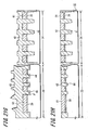
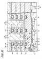
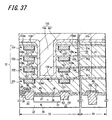
- FIG. 1 is a schematic view illustrating an exemplary CMOS solid-state imaging device provided with isolation regions formed with diffusion layers.
- a CMOS solid-state imaging device 101 including a pixel section 103 having plural pixels arranged on a semiconductor substrate 102, and a peripheral circuit section 104 including logic circuits, formed on the periphery of the pixel section 103.
- plural unit pixels 110 are disposed to be arrayed two-dimensionally, in which each of the unit pixels is formed, including a photodiode (PD) 107 serving as a photoelectric conversion element and several pixel transistors 108.
- PD photodiode
- These pixel transistors are representatively illustrated in FIG.
- a multilevel wiring layer 114 is formed above the pixel 110, including multiple wiring layers 113 having insulator films 112 formed thereunder for passivation, and an on-chip color filter 115 and an on-chip micro-lens 116 are formed on thus formed structure.
- another multilevel wiring layer is similarly formed in the peripheral circuit section 104, including multiple layers of wiring having insulator films formed thereunder.
- the isolation region 121 in the pixel section 103 is formed, including a p+ diffusion region 122 formed by ion implantations in the semiconductor substrate 102, and an insulator layer 123 of a silicon oxide film formed on the diffusion region.
- the insulator layer 123 is partially buried into the substrate 102, the buried depth h1 is set to be 50 nm or less, and the total thickness is set in the range approximately from 50 to 150 nm.
- an isolation region 125 is formed with the STI structure, consisting of a trench 126 disposed in the semiconductor substrate 102, and an insulator layer 127 of a silicon oxide film buried into the trench 126.
- the buried depth h2 of the insulating layer 127 into the substrate 102 is in the range approximately from 200 to 300 nm, and its protrusion height h3 protruded out of the substrate surface is sufficiently lower than the protrusion height h4 of the insulator layer 123 in the pixel section 103.
- an example of an isolation region formed in a pixel section is disclosed in Japanese Unexamined Patent Application Publication No. 2005-191262
- another example of isolation region in DRAM is disclosed in Japanese Unexamined Patent Application Publication No. 2007-288137 .
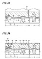
- the former of the abovementioned structures which forms the regions with the same STI structure in both the pixel section and the peripheral circuit section, is known to have a problem of increasing white spots. Namely, since the STI isolation regions in the pixel section are formed deep into the semiconductor substrate similarly to the STI isolation regions in the peripheral circuit section, the effects of stresses and damages exerted onto the photodiode increase, and this results in the increase of white spots. In order to suppress these white spots, the pinning (i.e., hole accumulation) has to be strengthened at the edges of the STI isolation regions.
- the latter of the abovementioned structures may be taken as a remedial measure, which forms the isolation region 121 including the p+ diffusion region 122 and the insulator layer 123 disposed on the diffusion region.
- the formation of the abovementioned diffusion region has to be included in addition to the processes of forming the isolation region 125 with the STI structure in the peripheral circuit section 104.
- the protrusion height h4 of the insulator layer 123 is relatively large in the isolation region 121 of the pixel section, there is a problem of generating a polysilicon residue 133a, etc.
- gate electrodes 131 (131A, 131B, 131C) of pixel transistors.
- the residue 133a of conductive polysilicon is formed with relative ease on the sidewall of the insulator layer 123 having a large step difference.
- the polysilicon residue 133a is formed, several adverse effects may arise such as short circuit failures between neighboring gate electrodes 131 of the pixel transistors and defects of imaging characteristics.
- the notations 131A, 131B, and 131C used in FIGS. 2A and 2B stand for gate electrodes of transfer, reset, and amplifying transistors, respectively.
- the notations 134 indicate n+ source/drain regions.
- the present invention provides a solid-state imaging device that enables reducing the number of production processes and improving pixel characteristics including the sensitivity, and a production method thereof.
- this invention provides an electronic device incorporating the solid-state imaging device.
- the invention provides a solid-state imaging device as defined in claim 1, a method of manufacturing it as defined in claim 4 and an electronic device as defined in claim 8.
- the solid-state imaging device including a pixel section, a peripheral circuit section, a first isolation region formed with the STI structure on a semiconductor substrate in the peripheral circuit section, and a second isolation regions formed with the STI structure on the semiconductor substrate in the pixel section.
- the second isolation region in the pixel section is formed such that the portion thereof buried into the semiconductor substrate is shallower than the portion buried into the semiconductor substrate of the first isolation region and the height of the upper face thereof is equal to that of the first isolation region with the STI structure.
- the portion buried into the semiconductor substrate of the second isolation region in the pixel section is shallower than the portion buried into the semiconductor substrate of the first isolation region in the peripheral circuit section, so that adverse effects of stresses and damages onto the photoelectric conversion element are suppressed.
- the surface height of the second isolation region in the pixel section is made to be equal to and as low as that of the first isolation region in the peripheral circuit section, so that in fabricating gate electrodes after forming device separation regions, no electrode material remains on the sidewalls of the device separation regions. Because the surface height of the second isolation region in the pixel section is made equal to that of the first isolation region in the peripheral circuit section, the increase of processing steps due to the difference in the STI structures of the first and second isolation regions can be suppressed to a minimum.
- the film thickness of insulating interlayers from the surface of the photoelectric conversion element to the wiring on the lowermost layer is decreased.
- the distance between the photoelectric conversion element and an on-chip micro-lens becomes small according to the abovementioned decrease in the film thickness, whereby the condensing efficiency is improved.
- the surface height of second isolation regions in the pixel section is brought to be equal to and as low as that of the first isolation regions in the peripheral circuit section, as mentioned above. Therefore, no electrode material remains on the sidewalls of the isolation regions during the gate electrode fabrication following the formation of the isolation regions.
- a method of producing the solid-state imaging device including the steps of (a) forming a first trench in the portion where an isolation region is to be formed in the peripheral circuit section on a semiconductor substrate and a second trench in the portion where another isolation region is to be formed in the pixel section on the semiconductor substrate, in which the second trench is shallower than the first trench, (b) forming a insulator layer over the structure including the interiors of the first and second trenches, and (c) forming first and second isolation regions to have the surface heights equal to each other through polishing the insulator layer.
- both the deposition of the insulator layer into the first trench formed on the side of the peripheral circuit section and the second trench formed on the side of the pixel section having a shallower depth than the first trench and the polishing of the insulator layer are performed in the same process, and the surface heights of the insulator layer, which is used for forming the first and second isolation regions, are brought to be equal to each other.
- the increase of the processing steps due to the difference in the STI structures of the first and second isolation regions can be suppressed to a minimum.
- the surface height of second isolation regions in the pixel section is brought to be equal to and as low as that of the first isolation regions in the peripheral circuit section, no electrode material remains on the sidewalls of the isolation regions during the gate electrode fabrication following the formation of the isolation regions. Since the second trenches on the side of the pixel section are formed to be shallower than the first trenches on the side of the peripheral circuit section, the adverse effects of stresses and damages can be suppressed, which are otherwise exerted by the second isolation regions onto the photoelectric conversion element.
- An electronic device including a solid-state imaging device, an optical system configured to lead incident light to a photoelectric conversion element included in the solid-state imaging device, and a signal processing circuit configured to process output signals from the solid-state imaging device.
- This solid-state imaging device includes a pixel section and a peripheral circuit section, in which first isolation regions are formed with the STI structure on a semiconductor substrate in the peripheral circuit section, and second isolation regions are formed with the STI structure on the semiconductor substrate in the pixel section.
- the second isolation regions in the pixel section are formed such that the portion thereof buried into the semiconductor substrate is shallower than the portion buried into the semiconductor substrate of the first isolation regions, and the height of the upper face thereof is equal to that of the first isolation regions with the STI structure.
- the portion buried into the semiconductor substrate of the second isolation region in the pixel section is shallower than the portion buried into the semiconductor substrate of the first isolation region in the peripheral circuit section, so that adverse effects of stresses and damages by the second isolation region onto the photoelectric conversion element are suppressed.
- the surface height of the second isolation region in the pixel section is made to be equal to and as low as that of the first isolation region in the peripheral circuit section, so that in fabricating gate electrodes after forming device separation regions, no electrode material remains on the sidewalls of the device separation regions. Because the surface height of the second isolation region in the pixel section is made equal to that of the first isolation region in the peripheral circuit section, the increase of the processing steps due to the difference in the STI structures of the first and second isolation regions can be suppressed to a minimum.
- the film thickness of insulating interlayers decreases and the condensing efficiency is improved.
- the portion of the second isolation regions buried in the semiconductor substrate in the pixel section is shallower than the portion of the first isolation regions buried in the semiconductor substrate in the peripheral circuit section. As a result, adverse effects onto the photoelectric conversion element due to stresses and damages by the second isolation region can be suppressed. Since the surface height of second isolation regions in the pixel section is brought to be equal to and as low as that of the first isolation regions in the peripheral circuit section, no electrode material remains on the sidewall of the isolation regions during the gate electrode fabrication following the formation of the isolation regions.
- the reduction of processes and the improvement in the pixel characteristic including sensitivity can be achieved.
- the solid-state imaging device is characterized by the configuration of isolation regions included in a pixel section and a peripheral circuit section of the imaging device.
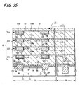
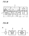
- FIG. 3 is a drawing generally illustrating a configuration of a solid-state imaging device or CMOS image sensor to which the an embodiment of present invention is applied.
- the solid-state imaging device 1 in this example is provided, including a pixel section 3 (so-called imaging section) having plural pixels 2 with plural photoelectric conversion elements regularly arranged in two-dimension on a semiconductor substrate 11 of silicon substrate, for example, and also including a peripheral circuit section.
- Each of the plural pixels 2 is formed, including a photodiode for example, serving as a photoelectric conversion element, and several pixel transistors (so-called MOS transistors).
- These pixel transistors are provided, including four transistors, for example, a transfer transistor, a reset transistor, an amplifying transistor, and a select transistor.
- the pixel transistors may alternatively be provided, including three transistors such as the transfer, reset, and amplifying transistors, excepting the select transistor. Since the equivalent circuit of a unit pixel is similar to the one in the past, a detailed description thereof is omitted herein.
- the peripheral circuit section is provided, including a vertical driving circuit 4, column signal processing circuits 5, a horizontal driving circuit 6, an output circuit 7, and a control circuit 8, etc.
- the control circuit 8 is configured to generate, based on vertical synchronizing signals, horizontal synchronizing signals, and the master clock, clock signals and control signals, which are used as the standard for the operation of the vertical driving circuit 4, column signal processing circuits 5, and horizontal driving circuit 6, and to input these generated signals to the vertical driving circuit 4, column signal processing circuits 5, horizontal driving circuit 6, etc.
- the vertical driving circuit 4 is provided, including shift registers, for example, and configured to selectively scan each of the pixels 2 included in the pixel section 3 sequentially row by row in the vertical direction, and to supply pixel signals based on signal charges generated corresponding to the amount of light received by the photoelectric conversion element in each pixel 2, i.e., photodiode in this example, to the column signal processing circuits 5 by way of vertical signal lines 9.
- the column signal processing circuits 5 are provided for example for respective columns of the pixels 2 included in the pixel section, and configured to implement various types of signal processing such as noise removal, which is performed by comparing, pixel column by column, a first group of the signals output from the pixels 2 on the presently selected column with a second group of the signals output from black reference pixels (disposed surrounding an effective pixel region). Namely, the column signal processing circuits 5 perform signal processing such as CDS (correlated double sampling) to remove fixed pattern noises inherent to the pixels 2, signal amplification, and other similar processes.
- CDS correlated double sampling
- the horizontal driving circuit 6 is provided, including shift registers, for example, and configured to sequentially select each of the column signal processing circuits 5 by successively outputting horizontal scanning pulses, and to output pixel signals from each of the column signal processing circuits 5 to the horizontal signal line 10.
- the output circuit 7 is configured to perform signal processing onto the signals successively supplied by each of the column signal processing circuits 5 through the horizontal signal line 10, and output the thus processed signals.
- a multilevel wiring layer is formed above the substrate surface on the side where the pixel section 3 and the peripheral circuit section are formed, having insulator films formed thereunder for passivation.
- an on-chip color filter is formed on the multilevel wiring layer having a planarizing film formed thereunder, and further thereon an on-chip micro-lens is formed.
- a shading film is formed in the regions other than pixel regions in the imaging section.
- the shading film is disposed in both the peripheral circuit section and the region in the imaging section other than the photodiodes (so-called photodetector parts).
- the shading film may be formed using the uppermost wiring layer of the multilevel wiring layer.
- the multilevel wiring layer is formed on the backside as the light incidence side (so-called light receiving surface). Namely, the multilevel wiring layer is formed on the surface side opposite to the light receiving surface.
- solid-state imaging device according to the present embodiments of the invention, and particularly the configuration of isolation regions formed therein, can primarily be adapted to CMOS solid-state imaging devices as described herein, it is not intended to limit the invention to those disclosed in the embodiments.
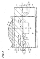
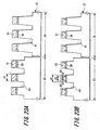
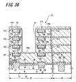
- FIG. 4 is a schematic view illustrating a solid-state imaging device according to a first embodiment of the present invention.
- the major portions of the imaging device are shown including a pixel section (so-called imaging region) 23 and a peripheral circuit section 24, respectively formed on a semiconductor substrate 22 such as a silicon substrate, for example.
- the solid-state imaging device 21 of the present embodiment is provided, including the pixel section 23 having a plurality of pixels arranged on the semiconductor substrate 22, and the peripheral circuit section 24 formed on the periphery of the pixel section 23 including logic circuits, for example.
- the pixel section 23 is provided with a plurality of unit pixels 25 arranged in a two-dimensional array, in which each of the unit pixels is formed, including a photodiode (PD) 26 serving as a photoelectric conversion element and several pixel transistors 27.
- PD photodiode
- pixel transistors are representatively illustrated in FIG. 4 by a single pixel transistor 27 for the purpose of clarity, and this pixel transistor 27 is formed, including source/drain regions 28, and a gate insulating film and a gate electrode (not shown).
- a multilevel wiring layer 33 is formed above the pixel 25, including multiple layers of wiring 32 having insulating interlayers 31 formed thereunder, and an on-chip color filter 34 and an on-chip micro-lens 35 are formed on thus formed structure.
- the peripheral circuit section 24 is provided with logic circuits which are formed, including CMOS transistors (not shown), for example, and with another multilevel wiring layer which is similarly formed, including multiple layers of wiring having insulating interlayers 31 formed thereunder. '
- the photodiode 26 is provided in a p-type (or a first conductivity type) semiconductor well region 36 of the semiconductor substrate 22, including a charge accumulation region 37 of n-type (or a second conductivity type opposite to that of the first conductivity type), an insulator film 39 formed on the surface of the accumulation region, and a p+ semiconductor region 38 (so-called hole accumulation layer) for controlling dark currents formed in the vicinity of the interface with a silicon oxide film, for example.
- a first isolation region 43 with the STI structure is formed by burying an insulator layer 42 in a trench 41, which is formed in advance vertically into the semiconductor substrate 22.
- a second isolation region 45 of the STI structure is formed by burying an insulator layer 42 in another trench 44, which is formed in advance vertically into the semiconductor substrate 22.
- the first isolation region 43 in the peripheral circuit section 24 is formed with a buried depth h5 of the buried portion of the insulator layer 42 in the semiconductor substrate ranging approximately from 200 to 300 nm, and with a height of the upper face of the portion thereof protruded from the surface of the semiconductor substrate 22, i.e., protrusion height h6, ranging approximately from 0 to 40 nm.
- the buried depth h5 is herein measured as the distance from the surface of the semiconductor substrate 22 under the insulator film 39, and the protrusion height h6 is the height measured also from the surface of the semiconductor substrate 22 under the insulator film 39.
- the buried depth h7 of the portion buried into the insulator layer 42 of the semiconductor substrate is formed to be shallower than the buried depth h5 on the side of the peripheral circuit section 24.
- this second isolation region 45 is formed to have a height of the upper face of the portion of the insulator layer 42 protruded from the surface of the semiconductor substrate 22, i.e., a protrusion height h8, that is approximately equal to the protrusion height h6 on the side of the peripheral circuit section 24.
- the second isolation region 45 can therefore be formed to have the protrusion height h8 ranging approximately from 0 to 40 nm, the buried depth h7 ranging approximately from 50 to 160 nm, and the total thickness h9 ranging approximately from 70 to 200 nm.
- the protrusion height h6 of the first isolation region 43 is necessary to be in the range approximately from 0 to 40 nm from restrictions on the ordinary MOS structure.
- the protrusion height h8 of the second isolation region 45 is set to be in the range approximately from 0 to 40 nm in conformity with the protrusion height h6 on the side of the peripheral circuit section 24.
- the total thickness h9 ranging approximately from 70 to 200 nm as described above is needed for the second isolation region 45 from restrictions on pixel characteristics.
- This total thickness h9 of the second isolation region 45 in the pixel section 23 is sufficient to yield satisfactory device isolation characteristics, not to form a parasitic MOS transistor even after wirings are formed on the insulator layer 42, and not to exert adverse effects on the photodiode 26 such as stress and damage.
- the total thickness h9 is within the range between 70 and 200 nm, satisfactory device isolation characteristics of the isolation region 45 are obtained and the generation of white spots can be suppressed.
- the heights, h6 and h8, of the first and second isolation regions that these heights are defined as the same if they are found equal to each other within the limits of the processing variation based on manufacture processing accuracy.
- the wafer in-plane variation of about ⁇ 10% is generally present for the nitride film with a thickness in the order of 200 nm.
- polishing by CMP chemical mechanical polishing
- both the second isolation region 45 in the pixel section 23 and the first isolation region 43 in the peripheral circuit section 24 are made in the STI structure, and the protrusion heights h6 and h8 of respective insulating layers 42 from the surfaces of the semiconductor substrate 22 are made the same. Since the process steps of burying the insulator layer 42 and planarizing the insulator layer 42 can be simultaneously carried out in production, owing to this configuration, the number of processes can be reduced.
- the protrusion height h8 for the second isolation region 45 in the pixel section 23 is formed to be comparable with the protrusion height h6 of the first isolation region 43 in the peripheral circuit section 24, i.e., to be sufficiently small, so that the film thickness of the insulating interlayer between the photodiode 26 and the first layer wiring becomes small. Accordingly, the distance L2 between the photodiode 26 and the on-chip micro lens 35 becomes smaller than the distance L1 shown earlier in FIG. 1 . As a result, the condensing efficiency to the photodiode 26 is improved and the sensitivity is improved.
- its protrusion height h8 above the substrate is in the range from 0 to 40 nm, which is as small as the protrusion height h6 of the first isolation region 43 in the peripheral circuit section 24.
- the second isolation region 45 is formed with the STI structure so that the buried depth h7 of the portion of the second isolation region 45 buried into the semiconductor substrate 22 is shallower than the buried depth h5 of the first isolation region 43 with the STI structure into the semiconductor substrate 22 on the side of the peripheral circuit section 24.
- the buried depth h7 of the second isolation region 45 in the pixel section 23 is set to be in the range from 50 nm to 160 nm. This buried depth h7 does not exert adverse effects such as stress and damage on the photodiode 26. That is, the generation of defects can be prevented since the depth of the trench 44 is small.
- the generation of the electrons at the interface between the second isolation region 45 and the photodiode 26 can be suppressed, which is a factor in causing white spots otherwise.
- the leak of the electrons into the photodiode 26 from the interface with the second isolation region 45 is suppressed, whereby the appearance of the white spots in the photodiode 26 can be suppressed.
- the total thickness h9 of the second isolation region 45 in the pixel section 23 is in the range approximately from 70 and 200 nm, sufficient device isolation characteristics can be obtained.
- the parasitic MOS transistor may not be formed even when wirings are formed extending above the second isolation region 45.
- the device isolation characteristics can be secured even if the concentration of p-type ions at the edge portion (transverse end portion) of the second isolation region 45 in the pixel section 23 is relatively low, it is advantageous for reading out from the transfer transistor in comparison with the related art configuration having a diffusion layer isolation region shown in FIGS. 2A and 2B .
- the above noted p-type region is formed in the isolation region adjacent to the transfer transistor in the pixel.
- the protrusion height h8 of the second isolation region 45 in the pixel section 23 becomes the same as the protrusion height h6 of the first isolation region 43 in the peripheral circuit section 24, i.e., sufficiently small, the distance L2 between the photodiode 26 and the on-chip micro lens 35 becomes smaller than the distance L1 shown in FIG. 1 . As a result, the condensing efficiency to the photodiode 26 is improved and the sensitivity is improved.
- Both the second isolation region 45 in the pixel section 23 and the first isolation region 43 in the peripheral circuit section 24 are each configured to be the STI structure, having the same protrusion heights, h6 and h8, for respective insulator layers 42 from the surface of semiconductor substrate 22. Since the process steps of burying and planarizing the insulator layers 42 can be carried out simultaneously with this configuration, the number of processes can be reduced.
- the reduction in the number of processes in the manufacturing process becomes feasible and pixel characteristics can be improved through the improvement in afterimage characteristics and in the amount of saturation signals, the short circuit prevention between pixel transistors, etc.
- no polysilicon residue is formed during the fabrication of gate electrodes with a polysilicon film, on the sidewall of the portion of the insulator film 42 protruded out of the substrate surface, the insulator film 42 forming the second isolation region 45 in the pixel section 23. Thereby, the processing of gate electrodes can be carried out with more ease and manufacturing yield is improved.
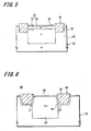
- FIG. 6 illustrates the solid-state imaging device according to a second embodiment of the present invention.
- FIG. 6 is a cross section illustrating the major portions of the imaging device configuration primarily including the photodiode 26 in the pixel section 23 and the second isolation region 45 adjacent thereto.
- the solid-state imaging device 48 is provided with a p-type semiconductor layer 49 formed at least in the region in contact with the photodiode 26 in the second isolation region 45 of the pixel section 23.
- the p-type semiconductor layer 49 is formed, extending onto the side face in contact with the photodiode 26 and a part of the underside of the insulator layer 42 in the second isolation region 45.
- the p-type semiconductor layer 49 may alternatively be formed extending onto the entire side face and underside of the insulator layer 42 buried in the semiconductor substrate 22 as indicated by chain lines in the drawing.
- the p-type semiconductor layer 49 may be formed by conducting ion implantations of impurities, for example. ,
- the formation of the p-type semiconductor layer 49 may also be carried out by ion implantations into the trench either after completion of the trench in the course of the STI structure formation, or after completing the STI structure, through the insulator layer 42 from above.
- the p-type semiconductor layer 49 is formed by ion implantations following the formation of the insulator layer 42, when the depth of the insulating layer 42 is too deep, a difficulty may arise in distributing p-type impurity ions properly even after implanting the ions at any implant angle.
- the insulator layer 42 is formed relatively shallow and a little bit tapered, namely such that its width is gradually narrowed downward. Since the other parts of the configuration are similar to those mentioned earlier with reference to FIGS. 3 and 4 , the repeated description thereof is omitted herein.
- the p-type semiconductor layer 49 is formed in the vicinity of the interface between the insulator layer 42 and the photodiode 26 in the second isolation region 45 of the pixel section 23, the generation of the electrons at the device isolation interface can be suppressed further and the generation of the white spots in the photodiode 26 can also be suppressed.
- the effects similar to those described earlier with the configuration according to the first embodiment can also be offered with the present structure.
- FIG. 7 illustrates the solid-state imaging device according to a third embodiment of the present invention.
- FIG. 7 is a cross section illustrating the major portions of the imaging device primarily including the photodiode 26 in the pixel section 23 and the second isolation region 45 adjacent thereto.
- the solid-state imaging device 51 is provided, in the second isolation region 45 of the pixel section 23, further including a p-type semiconductor layer 52 formed under the insulator layer 42 for also serving as diffusion layer isolation.
- the p-type semiconductor layer 49 shown in FIG. 7 is formed at least in the vicinity of the interface between the photodiode 26 and the insulator layer 42 in a manner similar to FIG. 6 .
- the device configuration may alternatively be provided without the p-type semiconductor layer 49. Since the other parts of the configuration are similar to those mentioned earlier with reference to FIGS. 4 , 5, and 6 , the repeated description thereof is omitted herein.
- the p-type semiconductor layer 52 is further formed under the insulator layer 42 to provide the diffusion layer isolation in the second isolation region 45 in the pixel section 23
- device isolation characteristics of the second isolation region 45 in the pixel section 23 are further improved merging with the abovementioned diffusion layer isolation.
- the effects similar to those described earlier with the configuration according to the first and second embodiments can also be offered with the present structure.
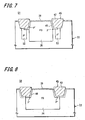
- FIG. 8 illustrates the solid-state imaging device according to a fourth embodiment of the present invention.
- FIG. 8 is a cross section illustrating the major portions of the imaging device primarily including the photodiode 26 in the pixel section 23 and the second isolation region 45 adjacent thereto.
- the solid-state imaging device 54 is provided, in the pixel section 23, forming the second isolation region 45 with the STI structure shallower than that on the side of the peripheral circuit section 24 as in the above-described embodiments and extending the photodiode 26 such that at least part thereof comes underneath the second isolation region 45.
- the p-type semiconductor layer 49 similar to that shown in FIG. 6 can be formed in the vicinity of the interface between the second isolation region 45 and at least the photodiode 26.
- the device configuration may alternatively be provided without the p-type semiconductor layer 49.
- the p-type semiconductor layer 52 for serving as the diffusion layer isolation may be formed under the insulator layer 42 in the second isolation region 45. Since the other parts of the configuration are similar to those mentioned earlier with respect to the first and second embodiments, the repeated description thereof is omitted herein.
- the photodiode 26 is formed to be extended such that at least a part thereof comes underneath the second isolation region 45, the area of the photodiode 26 can be increased. This increase in the photodiode area is advantageous for increasing the amount of saturation signals and improving the sensor sensitivity.
- the effects similar to those described earlier with the configuration according to the first through third embodiments can also be offered with the present structure.
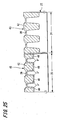
- FIG. 9 illustrates the solid-state imaging device according to a fifth embodiment of the present invention.
- FIG. 9 is a cross section illustrating only the major portions of the imaging device including the photodiode 26 in the pixel section 23, the pixel transistor 27 and the second isolation region 45 adjacent thereto, and the first isolation region 43 in the peripheral circuit section 24.
- the first isolation region 43 with the STI structure in the peripheral circuit section 24 is formed deep in the vertical direction in the semiconductor substrate 22.
- the second device separation region 45 with the STI structure in the pixel section 23 is formed in the vertical direction in the semiconductor substrate 22 shallower than the first isolation region 43.
- the protruded heights h8 and h6 from the surfaces of the semiconductor substrate 22 of the insulator layer 42 of the first isolation region 43 and the insulator layer 42 of the second isolation region 45 are the same.
- an insulator section 42a in a bird's beak shape extending from the insulator layer 42 is provided in each of the parts of the first isolation region 43 and the second isolation region 45 contacting the surfaces of the semiconductor substrate 22. That is, respective shoulder portions of the insulator layers 42 of the first isolation region 43 and the second isolation region 45 contacting the surfaces of the semiconductor substrate 22 form the insulator sections 42a each in a bird's beak shape, and the shoulder portions of the semiconductor substrate 22 are covered by the insulator sections 42a with thick film thicknesses. Also, because of the insulator sections 42a each in a bird's beak shape, the curvatures of the insulator layers 42 in the shoulder portions are gentle.
- insulator films other than the thermally-oxidized film, such as, a plasma-oxidized film, a plasma-oxynitrided film, etc., formed by insulating processing, such as plasma oxidizing processing, plasma oxynitriding processing, etc., may be used.
- an impurity implanting region for suppressing dark currents i.e., a p-type semiconductor layer 49
- a p-type semiconductor layer 49 is formed from the interface with the semiconductor substrate 22 to a part of the surface side of the semiconductor substrate 22. That is, the p-type semiconductor layer 49 is formed along the bottom and side surfaces of the insulator layer 42 inlaid in the second isolation region 45 to the insulator sections 42a each in a bird's beak, partly extending in the lateral direction in the area reaching the semiconductor substrate surface.
- a gate electrode 56 is formed so as to ride on a protruded surface protruded from the surface of the second isolation region 45.
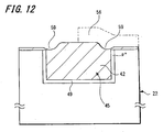
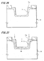
- the insulator section 42a in a bird's beak shape is formed in the upper corner part (shoulder part) of the trench 44 of the second isolation region 45 with the STI structure in the pixel section 23 . That is, because the insulator section 42a in a bird's beak shape is provided as shown in FIG. 10 , a divot 59 shown in FIG. 12 that occurs in the isolation region 45 with the ordinary STI structure is suppressed.
- end portions of the gate electrode 56 are formed so as to ride on the isolation region.
- the thickness t1 of the insulator layer 42 at the upper corner portion of the trench 44 being large and the stress being lessened due to the gentle curvature of the upper corner portion combine to make the electric field concentration to the upper corner portion of the trench 44 to be lessened.
- Lessening of the electric field concentration increases the threshold voltage Vth in the upper corner portion and can suppress generation of a parasitic channel component 57 at an edge portion on the boundary with the second isolation region 45 of the pixel transistor 27 shown in FIG. 11 . Because the generation of the parasitic channel component 57 is suppressed, leak current between the source S and the drain D is suppressed and random noise can be reduced.
- the oxide film quality in the edge portion is not relatively good compared with the center portion, random noise can be reduced. Because the divot 59 is suppressed, a hump in the ⁇ Id (drain current) - Vg (gate voltage) ⁇ characteristic of the pixel transistor 27 can be reduced.
- the curvature of the upper corner portion of the trench 44 is gentle in the second isolation region 45 of the pixel section 23, the stress given to the upper corner portion is reduced. Thereby, dark currents and white spots attributed to the floating diffusion (FD) section of the pixel can be improved. Also, junction leak in the floating diffusion section is suppressed.
- FD floating diffusion
- the p-type semiconductor layer 49 is provided around the STI structure.
- the p-type semiconductor layer 49 is formed from the sidewall of the trench 44 to the surface side of the semiconductor substrate, that is, the p-type semiconductor layer 49 is formed extending toward the active region side of the photodiode or pixel transistor.
- the p-type semiconductor layer 49 is provided also to the active region side in the upper portion of the trench 44, so that the freedom of enabling improvement of dark currents and white spots is increased.
- the parasitic channel component can be made further smaller. Combined with the above-described divot improvement, random noise can be improved in a synergistic manner. Moreover, similar effects described in the first embodiment are produced.
- FIGS. 13A through 17J a first embodiment of the production method for the solid-state imaging device according to the present invention will be described with reference to FIGS. 13A through 17J .
- the present embodiment is adapted to producing the solid-state imaging device according to the aforementioned second embodiment of the solid-state imaging device shown in FIG. 6 , in particular to forming isolation regions thereof.
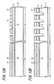
- a thin insulator film 39 is formed having a first predetermined film thickness on a major surface of a semiconductor substrate 22, and subsequently formed on the insulator film 39 is another insulator film 61 having a second predetermined film thickness with an etching rate different from that of the insulator film 39.
- a silicon oxide film may be used, for example.
- a silicon nitride film formed by low pressure CVD of about 100 nm in film thickness may be used, for example.
- a photoresist film is deposited over the insulator film 61.
- This photoresist film is exposed through an optical' mask having a prescribed pattern and subsequently developed, whereby a resist mask 63 is formed, having openings 62 corresponding to the portions into which isolation regions on the side of the peripheral circuit section 24 are to be formed.
- a resist mask 63 is formed, having openings 62 corresponding to the portions into which isolation regions on the side of the peripheral circuit section 24 are to be formed.
- the entire surface on the side of the pixel section 23 is covered by a flat face resist mask 63 having no opening.
- the insulator films 61 and 39 on the side of the peripheral circuit section 24 are removed by performing selective etching through the resist mask 63, and portions of the semiconductor substrate 22 are subsequently removed by further performing selective etching to obtain a predetermined depth, whereby several trenches 41 are formed.
- These trenches 41 are formed herein as relatively deep trenches having the depth ranging approximately from 200 to 300 nm, as mentioned earlier.
- a new photoresist film is deposited after removing the resist mask 63, as illustrated in FIG. 14C .
- This photoresist film is exposed through an optical mask having a prescribed pattern and subsequently developed, whereby a resist mask 65 is completed, having openings 64 corresponding to the portions into which isolation regions on the side of the pixel section 23 are to be formed.
- the entire surface on the side of the peripheral circuit section 24 is covered by a flat face resist mask 65 having no opening.
- the insulator films 61 and 49 on the side of the pixel section 23 are removed by performing selective etching through the resist mask 65, and portions of the semiconductor substrate 22 are subsequently removed by further performing selective etching to obtain a predetermined depth, whereby several trenches 44 are formed.
- These trenches 44 are formed to be relatively shallow with the depth approximately ranging from 50 to 160 nm, as mentioned earlier.
- the trenches are formed by performing an etching process first to have the depth ranging approximately from 40 to 150 nm, and subsequently, through light etching etc., the final depth on completion is obtained in the abovementioned range approximately from 50 to 160 nm.
- the resist mask 65 is removed, as illustrated in FIG. 15E .
- the process may alternatively be reversed in which the shallow trenches 44 on the side of the pixel section 23 are formed first and the deep trenches 41 on the side of the peripheral circuit section 24 are formed afterwards.
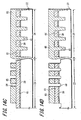
- p-type semiconductor layers 49 may be formed by ion implantations on the inner wall surface of the trenches 44.
- the p-type semiconductor layers 49 may alternatively be formed by ion implantations subsequent to the completion of isolation regions.
- the p-type semiconductor layers 49 may be formed by first implanting a first p-type impurity at the step of FIG. 15F and next implanting a second p-type impurity after completing isolation regions, whereby the p-type semiconductor layers 49 can be formed through the double ion implantation.
- a photoresist film is deposited over the entire surface of the structure, as illustrated in FIG. 15F .
- This photoresist film is exposed through an optical mask having a prescribed pattern and subsequently developed, whereby a resist mask 67 is formed only on the side of the peripheral circuit section 24.
- the insulator film 61 such as a silicon nitride film, for example, on the side of the pixel section 23 as a hard mask, ion implantations are conducted to implant p-type impurities 60 into the entire surface over the pixel section 23.
- No ion implantation of the p-type impurities 60 is conducted into the portions of the substrate 22, for which the insulator film 61 as the hard mask is formed, while the ion implantations are conducted into the portions of the substrate 22, for which the openings 61a are formed, i.e., into the inner wall surface of the trenches 44.
- the p-type semiconductor layers 49 are formed on the inner wall surface of the trenches 44, i.e., on the entire surface of the inner wall including the inner surface and bottom face of the wall of the trenches 44.
- These ion implantations are carried out by rotational implantations.
- the p-type semiconductor layers 49 may be formed only on the inner faces of the trenches, which are in contact with the photodiode, by an alternative implantation method.
- the p-type semiconductor layers 49 are formed by conducting ion implantations of p-type impurities because the trenches 44 have been formed, this has the potential to reduce the concentration of p-type impurities to implant, and the advantage of improving the electric charge Qs per a unit area as well.
- an insulator layer 42 is formed by the CVD method, for example, over the entire surface of the structure so as to be inlaid into the trenches 41 and 44.
- a silicon oxide film can be used, for example.
- the surface portions of the insulator layer 42 having rough surface irregularity are removed by partial etching in order to polish the entire surface uniformly. If there is a difference in the density of surface irregularity, an uneven finish of polish may arise after polishing the entire surface simultaneously. Therefore, the surface portions having rough surface irregularity are partially etched as illustrated in FIG. 16H .
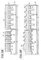
- the surface of the insulator layer 42 is subjected to a planarizing polish, as illustrated in FIG. 17I .
- the polishing step is terminated at the surface of the insulator film 61.
- the surface of the structure is polished so that the protrusion heights h6 and h8 of the insulator layer 42 are in the range approximately from 0 to 40 nm, about 40 nm in this example.
- the heights are set somewhat thicker so as to finally reach the range of 0 to 40 nm considering subsequent operations such as washing after polishing, etc.
- the CMP chemical mechanical polishing
- the insulator film 61 is removed by selective etching as illustrated in FIG. 17J .
- a photodiode 26 and pixel transistors 27 are formed, and formed further thereon is a multilevel wiring layer 33. Furthermore, on-chip color filters 34 and on-chip micro-lens 35 are formed on the multilevel wiring layer 33, having a planarizing film formed thereunder, whereby the intended MOS-type solid-state imaging device 48 is formed.
- the photodiode 26 may alternatively be formed before the process for forming the first isolation region 43 and the second isolation region 45.
- FIGS. 18A through 22 a second embodiment of the production method for the solid-state imaging device according to the present invention will be described with reference to FIGS. 18A through 22 .
- the present embodiment is adapted to producing the solid-state imaging device according to the aforementioned second embodiment of the solid-state imaging device shown in FIG. 6 , in particular to the isolation region thereof.
- a thin insulator film 39 is formed having a first predetermined film thickness on a major surface of a semiconductor substrate 22, and subsequently formed on the insulator film 39 is another insulator film 61 having a second predetermined film thickness with an etching rate different from that of the insulator film 39.
- a silicon oxide film may be used, for example.
- a silicon nitride film formed by the low pressure CVD of about 100 nm in film thickness may be used, for example.
- a photoresist film is deposited over the insulator film 61.
- This photoresist film is exposed through an optical mask having a prescribed pattern and subsequently developed, whereby a resist mask 73 is formed, having openings 711 and 722 corresponding to the portions into which isolation regions on the side of the peripheral circuit section 24 and on the side of the pixel section 23, are to be formed, respectively.
- the insulator films 61 and 39 on the side of the pixel section 23 and on the side of the peripheral circuit section 24, respectively, are removed by performing selective etching through the resist mask 73, and portions of the semiconductor substrate 22 are subsequently removed by further performing selective etching to obtain a predetermined depth, whereby several trenches 44 and 41a are formed, respectively.
- the trenches 41 are formed herein as relatively shallow trenches with the depth ranging approximately from 50 to 160 nm, as mentioned earlier.
- the trenches 41a on the side of the peripheral circuit section 24 are formed simultaneously with the trenches 44 on the side of the pixel section 23, the trenches 41a are formed as the trenches having approximately the same depth as the trenches 44.
- a new photoresist film is deposited after removing the resist mask 73, as illustrated in FIG. 19C .
- This photoresist film is exposed through an optical mask having a prescribed pattern and subsequently developed, whereby a resist mask 74 is formed, covering only the side of the pixel section 23. Namely, none of the resist mask 74 is formed on the side of the peripheral circuit section 24, while the entire surface on the side of the pixel section 23 is covered by the resist mask 74.
- the trenches 41a on the side of the peripheral circuit section 24 are further removed by etching through the resist mask 74, whereby the deep trenches 41 are formed. These trenches 41 are formed, having a depth approximately ranging from 200 to 300 nm, as mentioned earlier.
- p-type semiconductor layers 49 may be formed by ion implantations on the inner wall surface of the trenches 44.
- the p-type semiconductor layers 49 may alternatively be formed by ion implantations subsequent to the completion of isolation regions.
- the p-type semiconductor layers 49 may be formed by first implanting a first p-type impurity at the step of FIG. 20E and subsequently implanting a second p-type impurity after completing isolation regions, whereby the p-type semiconductor layers 49 can be formed through the double ion implantation.
- a photoresist film is further deposited after removing the resist mask 74, as illustrated in FIG. 20E .
- This photoresist film is exposed through an optical mask having a prescribed pattern and subsequently developed, whereby a resist mask 76 is formed only on the side of the peripheral circuit section 24.
- the insulator film 61 such as silicon nitride film, for example, on the side of the pixel section 23 as a hard mask, ion implantations are conducted to implant p-type impurities 60 into the entire surface over the pixel section 23.
- No ion implantation of the p-type impurities 60 is conducted into the portions of the substrate 22, for which the insulator film 61 as the hard mask is formed, while the ion implantations are conducted into the portions of the substrate 22, for which the openings 61a are formed, i.e., into the inner wall surface of the trenches 44.
- the p-type semiconductor layers 49 are formed on the inner wall surface of the trenches 44, i.e., on the entire surface of the inner wall including the inner surface and bottom face of the wall of the trenches 44.
- These ion implantations are carried out by rotational implantations.
- the p-type semiconductor layers 49 may be formed only on the inner faces of the trenches, which are in contact with the photodiode, by an alternative implantation method.
- FIGS. 20F through 22 Since subsequent steps illustrated in FIGS. 20F through 22 are similar to those illustrated earlier in FIGS. 16G through 17J , the portions corresponding to those shown in FIGS. 16G through 17J are shown with identical numerical representations and the repeated description thereof is omitted herein.
- a photodiode 26 and pixel transistors 27 are formed, and formed further thereon is a multilevel wiring layer 33. Furthermore, on-chip color filters 34 and on-chip micro-lens 35 are formed on the multilevel wiring layer 33, having a planarizing film formed thereunder, whereby the intended MOS-type solid-state imaging device 48 is formed.
- the photodiode 26 may alternatively be formed before the process for forming the first isolation region 43 and the second isolation region 45.
- the second and first isolation regions 45 and 43 are formed by depositing the insulator layer 42 and polishing by the CMP method in the same process. Therefore, the number of processes in the manufacturing process can be reduced.
- the second and first isolation regions 45 and 43 are formed, having the same projection height, and moreover having the depth of the second isolation region 45 on the side of the pixel section 23 shallower than the first isolation region 43 on the side of the peripheral circuit section 24.
- the solid-state imaging device can be produced with improved pixel characteristics in terms of afterimage characteristics, the amount of saturation signals, and other similar properties, as mentioned earlier.
- the present embodiment is adapted to producing the solid-state imaging device 55 according to the fifth embodiment shown in FIG. 9 , in particular, to forming the isolation region thereof.
- FIG. 23A shows a state that a thin insulator film 39 for example of a silicon oxide film is formed on the surface of a semiconductor substrate 22 where the trenches 44 and 41 are not formed and an insulator film 61 for example of a silicon nitride film is formed thereupon.
- the width of the insulator film 61 is selectively narrowed.
- the exposed surface of the insulator film 61 of a silicon nitride film is selectively removed for a predetermined thickness, and thereby the width is narrowed from the initial width d1 to the width d2.
- the removed width d3 can be made to be about 2 nm to 15 nm. If the removed width d3 is smaller than 2 nm, the effects of the present invention may not be obtained. If the width d3 is increased, the region where the gate oxide film of the active layer region edge becomes thicker increases, and the effective gate width of the transistor becomes narrow.
- the sidewalls and the semiconductor substrate side portions of the trenches 41 and 44 are subjected to thermal oxidation processing using the insulator layer 61 of a silicon nitride film for a mask. So-called sidewall oxidation of the trenches 44 and 41 are carried out. With this thermal oxidation processing, a thermally-oxidized film 71 is formed on the sidewalls of the trenches 44 and 41. Because this thermal oxidation is selective oxidation to the surface not covered by the insulator layer 61 of a silicone nitride film, as illustrated in FIG.
- thermally-oxidized film 71a in which the oxidized film bulges in a sort of bird's beak shape is formed.
- This thermally-oxidized film 71a in a bird's beak shape corresponds to the insulator section 42a in a bird's beak shape shown in FIG. 10 .
- the surfaces of the thermally-oxidized film in the upper corner portions of the trenches 44 and 41, contacting the semiconductor substrate 22 of silicon become gently rounded curvatures.
- the thermally-oxidized film in the lower corner portions of the trenches 44, 41 are rounded.
- a plasma-oxidized film, a plasma-oxynitrided film, etc. formed by selective insulating processing such as plasma oxidizing processing, plasma oxynitriding processing, etc. may be used. These plasma oxidation and plasma oxyniriding are selectively performed using the insulator film 61 for the mask.
- FIG. 24D in the state that the side of the peripheral circuit section 24 is covered by a resist mask, ion implantations of p-type impurities 60 are carried out, using the insulator film 61 of a silicon nitride film for the mask, to form a p-type semiconductor layer 49 on the internal wall surface of the trench 44 in the pixel section 23.
- This p-type semiconductor layer 49 is formed, as shown in FIG. 27 , in addition to the internal surface and bottom surface of the trench 44, so as to laterally extend from the upper corner portion of the trench 44. That is, the p-type semiconductor layer 49 is formed extending up to the surface of the semiconductor substrate 22 not covered by the insulator film 61.
- the process shown in FIG. 24D corresponds to the processes shown in FIG. 15F and FIG. 20E .
- the first isolation region 43 with a deep STI structure is formed in the peripheral circuit section 24 and the second isolation region 45 with a shallow STI structure is formed in the pixel section 23, in which the protrusion heights h8 and h6 in the pixel section 23 and the peripheral circuit section 24 are the same.
- the insulator layer 42 is inlaid into the trenches 41, 44, however, the insulator section 42a in a bird's beak shape is formed in each of the upper corner portions of the trenches 41, 44.
- the p-type semiconductor layer 49 is formed to surround the isolation region 45 and to partially extend in a lateral direction from the upper corner portion of the trench 44.
- a photodiode 26 and pixel transistors 27 are formed, and a multilevel wiring layer 33 is formed thereupon. Further, on-chip color filters 34 and on-chip micro-lenses 35 are formed on the multilevel wiring layer 33 through a planarizing film, and thereby the intended MOS type solid-state imaging device 55 is obtained.
- the width of the insulator film 61 of a silicone nitride film is narrowed by the process of FIG. 23B , and sidewall oxidation of the trenches 41, 44 is carried out by the process of FIG. 24C . That is, sidewall oxidation of the trenches 41, 44 is carried out, using the insulator layer 61 with the width thereof narrowed for the mask, to form the oxidized film 71. With this selective oxidation, in the upper corner portions of the trenches, the oxidized film 71a in a bird's beak shape in which the oxidized film has bulge is formed.
- the oxidized film 71a corresponds to the insulator section 42a in a bird's beak shape shown in FIG. 10 . Thereafter, the trenches 41, 44 are buried with the insulator layer 42, and thereby the first and second isolation regions 43, 45 are formed, so that divots that are generated in the ordinary isolation region of the STS structure can be reduced.
- the divot can be controlled, in the pixel transistors or MOS transistors in the peripheral circuit section, the film quality of insulator layers in separation edge portions can be improved, although the film quality is inferior to that of the gate oxidized film in the center portion. By eliminating the divot, the parasitic channel component is reduced, and random noise can be reduced.
- the sidewall oxidization can round the upper and lower corner portions of the trenches 41, 44.
- a surface with a gentle curvature is formed in each of the upper corner portions of the trench.
- the p-type semiconductor layer 49 is formed by ion implantations. At this time, the semiconductor layer 49 is formed extending from the sidewalls of the trenches to the surface of the semiconductor substrate in a lateral direction. Because the p-type semiconductor layer 49 is formed so as to extend to the substrate surface on the active region side in a lateral direction, it is possible to increase the freedom with which dark currents and white spots can be further improved.
- the p-type semiconductor layer 49 is formed so as to extend from the upper portion of the trench to the substrate surface side, the density of the p-type semiconductor layer 49 at the edge part in the upper portion of the trench becomes high. Thereby, the parasitic channel component at the edge part contacting the isolation region of the pixel transistor shown in FIG. 11 can be made further smaller. Combined with the improvement on the divot, random noise can be improved in a synergistic manner.
- An embodiment of the present invention can be applied to both the surface illumination type solid-sate imaging device and the backside illumination type solid-state imaging device.
- CMOS solid-state imaging device as previously described, an embodiment of the present invention can be applied to the surface side illumination type device in which light enters from the multilevel wiring layer side and the backside illumination type device in which light enters from the backside of the substrate opposite the multiple level wiring layer.
- the solid-state imaging devices according to an embodiment of the present invention can be applied to the linear image sensor, etc., in addition to the above-described area image sensor.
- FIG. 28 is a schematic view illustrating the solid-state imaging device according to a sixth embodiment of the present invention.
- the solid-state imaging device according to the present embodiment is provided, lowering the protrusion height h8 of the second isolation region in the pixel section to be the same as the protrusion height h6 of the first isolation region in the peripheral circuit section, and thinning or reducing the thickness of insulating interlayers formed between the substrate surface and a multilevel wiring layer.
- a waveguide structure is also provided facing the photodiode 26 to improve pixel characteristics including condensing efficiency of light led into the photodiode 26 and the overall sensitivity
- the solid-state imaging device 55 is provided in a manner similar to that described in the first embodiment, including a pixel section 23 having a plurality of pixels arranged on a semiconductor substrate 22, and a peripheral circuit section 24 formed on the periphery of the pixel section 23 including logic circuits, for example.
- the pixel section 23 includes plural pixels 25 arranged in a two-dimensional array, in which each of the pixels is formed, including a photodiode 26 serving as photoelectric conversion element, and pixel transistors 27.
- the photodiode 26 is provided, including a charge accumulation region 37 of n-type or the second conductivity type, an insulator film 39 formed on the surface of the accumulation region, and a p+ semiconductor region 38 for controlling dark current formed in the vicinity of the interface with a silicon oxide film, for example.
- a silicon nitride film 40 is formed for serving as an antireflection film.
- the pixel transistors are formed, which are representatively illustrated by a single pixel transistor 27 for the purpose of clarity, including source/drain regions 28, a gate insulator film 29, and a gate electrode 30 formed with polysilicon, for example.
- the source/drain regions 28 are formed in the direction perpendicular to the plane of the drawing sheet.
- the end portion of the gate electrode 30 is formed so as to ride over the second isolation region 45.
- the second isolation region 45 and first isolation region 43 are respectively formed with the STI structure described earlier.
- the first isolation region 43 is formed with an insulator layer 42 buried in a first trench 41, the insulator layer having a buried depth h5 and a protrusion height h6.
- the second isolation region 45 is formed with an insulator layer 42 buried in a second trench 44, the insulator layer having a buried depth h7 and a protrusion height h8.
- the protrusion heights h6 and h8 of the isolation regions 43 and 45 are set to be the same as mentioned earlier.
- the buried depth h7 of the second isolation region 45 is set to be shallower than the buried depth h5 of the first isolation region 43.
- the buried depth h5 may be in the range approximately from 200 to 300 nm, and the protrusion height h6 may be in the range approximately from 0 to 40 nm.
- the buried depth h7 may be in the range approximately from 50 to 160 nm
- the protrusion height h8 may be in the range approximately from 0 to 40 nm
- the total thickness h9 may be in the range approximately from 70 to 200 nm.
- a multilevel wiring layer 33 is formed, including multiple wiring layers 32 (321 to 324) having insulating interlayers 31 (311 to 315) formed thereunder for passivation.
- the insulating interlayers 31 can be formed with silicon oxide films, for example.
- the multiple wiring layers 32 are formed including a first-layer wiring 321, second-layer wiring 322, third-layer wiring 323, and fourth-layer wiring 324, in the present example.
- Each of the wiring layers 32 (321 through 324) is formed by the damascene process, burying a barrier metal layer 157 including tantalum/tantalum-nitride and a copper (Cu) wiring layer 158.
- first through fourth interlayer wiring diffusion prevention films 159 are formed for preventing the diffusion of copper (Cu) used as the wiring material.
- the wiring diffusion prevention films 159 are formed of films including SiN and/or SiC, for example. In the present example, the wiring diffusion prevention films 159 are formed of SiC films.
- the peripheral circuit section 24 is provided with logic circuits which are formed, including CMOS transistors, for example, and with other multilevel wiring layers which are similarly formed, having a predetermined number of wiring layers.
- a waveguide 156 is formed above each photodiode 26 in the pixel section 23 for leading incidence light efficiently to the photodiode 26.
- the waveguide 156 is formed by first forming a concave groove 87 in the portion of the multilevel wiring layer 33 facing the photodiode 26 by selectively etching the insulating interlayer 31 together with the interlayer wiring diffusion prevention films 159, and subsequently burying a first core layer 88 and a second core layer 89 into the concave groove 87.
- the plane 156a of the waveguide 156 facing the photodiode 26 is formed so as to terminate at the wiring diffusion prevention film 159a on the lowermost layer. Namely, the waveguide 156 is formed to reach the wiring diffusion prevention film 159a of the lowermost layer, and not to pass through the wiring diffusion prevention film 159a of the lowermost layer.
- a planarizing film 90, an on-chip color filter 34, and an on-chip micro lens 35 are formed in the pixel section 23.
- the thickness of insulating interlayers t1 is set to be small in the present embodiment, in which this thickness of insulating interlayers is measured from the surface of the semiconductor substrate 22 (i.e., the surface of the photodiode 26) to the lowermost wiring diffusion prevention film 159a, inclusive of the insulator film 39, antireflection film 40, and the first layer insulating interlayer 311. That is, in order to yield the high sensitivity at blue light wavelengths, the film thickness t1 is set to be in the range either from 220 to 320 nm, from 370 to 470 nm, or from 530 to 630 nm. As shown in FIG.
- the sensitivity can be obtained as high as approximately equal to, or greater than x + [(y - x)/ 2], where the variable x is the sensitivity value at a crest of the curve, and y is the value at a next trough.
- the present configuration of the multilevel wiring layer 33 and antireflection film 40 formed on the surface of the photodiode 26 is the more detailed one of the aforementioned configuration according to the first embodiment.
- the protrusion height h8 of the second isolation region 45 in the pixel section 23 is formed to be the same as the protrusion height h6 of the first isolation region 43 in the peripheral circuit section 24, i.e., as low as 40 nm or less.
- the film thickness t1 can be formed to be thin measured from the surface of the photodiode 26 to the wiring diffusion prevention film 159a on the lowermost layer in contact with the bottom of the waveguide 156, inclusive of the insulating interlayers (39, 40, 32).
- the insulating interlayer 31 is limited in its minimum film thickness so as not to induce the deposition of a polysilicon gate electrode on the isolation region 45 with the STI structure during the polishing process subsequent to the formation of the insulating interlayer.
- the protrusion height h8 of the second isolation region 45 in the pixel section 23 to be the same as the protrusion height h6 of the first isolation region 43 in the peripheral circuit section 24, the variation in the film thickness during the polishing process can be suppressed and the polishing process becomes feasible for attaining the film thickness d1 as small as 90 nm from the upper face of the gate electrode.
- the protrusion height h8 is assumed to be 30 nm
- the whole insulating interlayer can be processed to reduce its film thickness smaller by about 70 nm from the thickness in a first comparative example shown in FIG. 30 .
- the protrusion height h3 of the isolation region 43 with the STI structure in the peripheral circuit section 24 is considered to be 30nm, while the protrusion height h4 of the isolation region 45 with the STI structure in the pixel section 23 is also considered to be 80nm.
- the amount of polishing has to be appropriately controlled. Consequently, the finished film thickness t2 of the insulating interlayer is obtained as about 650 nm and the optimization of sensor sensitivity may not be achieved as a result.
- other regions shown in FIG. 30 similar to those in FIG. 28 are shown with identical numerical representations for purposes of comparison and the repeated description thereof is herein omitted.
- the condensing efficiency of the incidence light to the photodiode 26 is improved, and the sensor sensitivity, particularly the blue light sensitivity can be improved.
- FIG. 29 shows graphical plots of the sensitivity variation for respective colors, red, green, and blue, as a function of the insulating interlayer thickness t1 measured from the surface of the photodiode 26 (silicon surface) to the wiring diffusion prevention film 159a formed of SiC with the configuration of the solid-state imaging device according to the sixth embodiment, in which the curve R shows the sensitivity variation for red wavelengths, the curve G for green, and the curve B for blue.
- the silicon oxide film 39 is formed on the Si surface, the silicon nitride film 40 is formed further thereon, and the total thickness of both films, 39 and 40, is in the range of about 70 nm.
- the total thickness of the films, 39 and 40 may be formed to be in the range approximately from 20 to 120 nm.
- the refractive index of thus formed insulating interlayer is in the range from 1.4 to 1.5.
- the sensitivity is improved for the blue color, which normally has a low luminous efficiency, and the sensor sensitivity is most increased for the film thickness t1 in the range either from 220 to 320nm, from 370 to 470 nm, or from 530 to 630 nm.
- the sensitivity that is equal to or greater than the half of the sensitivity difference between the crest and trough of the sensitivity curve can be obtained.
- the diffraction of light takes place when the waveguide structure is included, primarily from the difference in refractive indices between (a) the material buried in the waveguide, i.e., a second core layer 89, and (b) the insulating interlayers formed from the surface of the photodiode 26 to the lowermost wiring diffusion prevention film 159a (that is, the interference of incident light is caused by the change of the refractive indices, and results in either reinforcing or weakening the incident light, depending on the range in insulator film thickness).
- this optimum range of film thickness can be set in the range either from 220 to 320nm, from 370 to 470 nm, or from 530 to 630 nm.
- the protrusion height of the isolation region is high on the side of the pixel section, the reflection of incident light is caused by the protrusion of the isolation region, and the sensor sensitivity decreases, accordingly.
- the protrusion height of the second isolation region on the side of the pixel section is low, the reflection of incident light by the protrusion decreases, and the sensor sensitivity can be improved.
- both the films, 39 and 40 when both the films, 39 and 40, are formed having a total film thickness approximately ranging from 20 to 120 nm, the above-mentioned range of film thickness t1, 220 to 320 nm, 370 to 470 nm, and 530 to 630 nm, changes with the total film thickness as follows.
- the total film thickness of both the films, 39 and 40 becomes smaller than 70 nm (20 nm, for example)
- the peak position of the sensitivity curve of FIG. 29 shifts to the left in the drawing (in the direction to increasing the film thickness of the insulating interlayer 311) relative to the peak position at the 70 nm thickness.
- the peak position of the sensitivity curve of FIG. 29 shifts to the right (in the direction to decreasing the film thickness of the insulating interlayer 311) relative to the peak position at the 70 nm thickness.
- the amount of the shift corresponding to the thickness is obtained as (70 - dN) x (nN - nO).
- the above notations are dN for the total film thickness of the films 39 and 40, nN for the refractive index of the silicon nitride film 40, and nO for the refractive index of the silicon oxide film 39.
- the generation of the white spots in the photodiode 26 is suppressed and the sensor sensitivity can be further improved, as described earlier in the first embodiment, comparing with the other configuration, in which the isolation region in the pixel section is formed, having the same buried depth as the region in the peripheral circuit section.
- the depth of the waveguide can be kept constant.
- the protrusion height of the isolation region on the side of the pixel section is large as illustrated in the first comparative example, it is conceived that, even after the formation and the subsequent step of planarizing polish of the insulating interlayers, the uniform planarization of the upper face of the structure is hard to be achieved because of relatively large step height and that the planarization of the wiring diffusion prevention film formed on the structure is also hard to be achieved.
- the process proceeds further in this situation for forming the multilevel wiring layer and subsequently forming the groove for the waveguide in the multilevel wiring layer, it becomes difficult to form the groove so as to be terminated accurately at the lowermost wiring diffusion prevention film.
- the waveguide may not be formed properly so as to be terminated at the lowermost wiring diffusion prevention film.
- the planarization polishing of the insulating interlayers is feasible, and proper waveguides can be formed so as to terminate at the lowermost wiring diffusion prevention film even in the device configuration with miniaturized pixels.
- the effect can be achieved of improving the difference in sensitivity between the middle and the circumference of a screen, so-called shading.
- the effects similar to those described earlier with the configuration according to the first embodiment can also be offered with the present structure, including the increase in sensor sensitivity, improvement in afterimage characteristics and in the amount of saturation signals, prevention of short circuit failures caused between pixel transistors, reduction of the number of processes, improvement of manufacturing yield, etc.
- optimal film thickness t1 in the range either from 220 to 320nm, from 370 to 470 nm, or from 530 to 630 nm, can be applied not only to the sixth embodiment, but also to the first through fourth embodiments as well.
- FIGS. 31 and 32 are schematic views illustrating a solid-state imaging device according to a seventh embodiment of the present invention.
- FIG. 31 is a simplified plan view of the layout of pixels in an imaging region as the major portion of the solid-state imaging device.
- FIG. 32 is a cross-sectional view taken along the line A-A of the structure of FIG. 31 .
- the solid-state imaging device 171 of the present embodiment is provided, including a pixel section 23 and a peripheral circuit section 24, in which the pixel section 23 includes a plurality of pixels 172 arranged in a two-dimensional array, each of the pixels being formed, including a photodiode (PD) 26 and several pixel transistors. As illustrated by the layout shown in FIG. 31 , each of the pixels 172 is formed in the present embodiment, including a photodiode (PD) 26 and several transistors, i.e., three transistors such as a transfer transistor Tr1, a reset transistor Tr2, and an amplifying transistor Tr3.
- the transfer transistor Tr1 is formed, including a source/drain region 173 serving as a floating diffusion (FD) and a transfer gate electrode 176 formed having a gate insulator film formed thereunder.
- the reset transistor Tr2 is formed, including a pair of source and drain regions 173 and 174, and a reset gate electrode 177 formed having another gate insulator film formed thereunder, in similar manner as above.
- the amplifying transistor Tr3 is formed, including a pair of source and drain regions 174 and 175, and an amplification gate electrode 178 formed having still another gate insulator film formed thereunder.
- an isolation region 86 of p-type impurity region is formed around the circumference of the photodiode (PD) 26.
- the photodiode (PD) 26 is isolated utilizing pn junction with the isolation region 86.
- the region of the pixel transistors such as the transfer transistor Tr1, reset transistor Tr2, and amplifying transistor Tr3, is isolated using the second isolation region 45 with the same STI structure as mentioned earlier.
- the vignetting of light is eliminated and the sensor sensitivity can be further improved. Namely, since the protrusion portion (with protrusion height h8) in the second isolation region 45 is not present by the photodiode (PD) 26, the vignetting of light is not caused by the protrusion portion and the light condensing efficiency is further improved.
- the isolation tolerance is improved and gate parasitic capacitance can be reduced.
- the pixel configuration is adapted herein above to include one photodiode and several pixel transistors
- the configuration may alternatively be formed for the structure having plural pixels shared with each other, for example, in which the circumference of the photodiode PD is isolated by pn-junction similarly to the seventh embodiment, while other portions are isolated using the second isolation region 45 with the aforementioned STI structure.
- the present configuration of pn junction isolation of the photodiode (PD) in the circumference thereof can also be applied to the solid-state imaging device according to the first through seventh embodiments as well.
- FIGS. 33 through 37 a fourth embodiment of the production method for the solid-state imaging device according to the present invention will be described with reference to FIGS. 33 through 37 .
- the present embodiment is adapted to producing the solid-state imaging device 55 according to the aforementioned sixth embodiment shown in FIG. 28 , in particular to forming insulating interlayers and waveguides thereof.
- Reference numerals 49 and 52 denote a p-type semiconductor region and a p-type semiconductor layer, respectively.
- shallow trenches 44 and deep trenches 41 are first formed in the pixel part 23 and the circumference circuit part 24, respectively, by way of process steps illustrated in either FIGS. 13A through 15E or FIGS. 18A through 19D .
- the second isolation region 45 and the first isolation region 43 each with the STI structure are formed by burying an insulator film 42 into the trenches 44 and 41, respectively, so as to make the protrusion heights h6 and h8 the same.
- a photodiode 26 and pixel transistors 27 are formed in the peripheral circuit section 24.
- an antireflection film 40 of silicon nitride film is formed on an insulator film 39 of a silicon oxide film covering the surface of the photodiode 26, an antireflection film 40 of silicon nitride film is formed. Thereafter, a first-layer insulating interlayer 311 of a silicon oxide film, for example, is formed by the CVD method for example, and is subsequently subjected to planarizing polish by the CMP method to obtain a desired film thickness t1.
- a first-layer wiring 321 is formed by burying a Cu wiring layer 158 into the trench 92, having a barrier metal layer 157 with tantalum/ tantalum-nitride formed thereunder for passivation.
- a first-layer wiring diffusion prevention film 159a for preventing the diffusion of the wiring 321 is formed of a SiC film or SiN film, for example, of a SiC film in this example.
- a second-layer insulating interlayer 312 there formed on the first-layer wiring diffusion prevention film 159a using process steps similar to those mentioned above, are a second-layer insulating interlayer 312, a second-layer wiring 322 having a barrier metal layer 157 and a Cu wiring layer 158 both buried into a trench 92, and a second-layer wiring diffusion prevention film 159b.
- a third-layer insulating interlayer 313, a third-layer wiring 323 having another barrier metal layer 157 and another Cu wiring layer 158 buried into a trench 92, and a third-layer wiring diffusion prevention film 159c are formed.
- a fourth-layer insulating interlayer 314, a fourth-layer wiring 324 having still another barrier metal layer 157 and a still another Cu wiring layer 158 buried into a trench 92, and a fourth-layer wiring diffusion prevention film 159d are formed.
- a fifth-layer insulating interlayer 315 is formed on the structure, whereby a multilevel wiring layer 33 is formed.
- a concave groove 87 is formed by selectively etching the portion in the multilevel wiring layer 33 facing the photodiode 26 so as to terminate at the lowermost wiring diffusion prevention film 159a as the first layer. This selective etching is performed on the insulating interlayer 315 on the fifth layer, the wiring diffusion prevention film 159d and insulating interlayer 314 on the fourth layer, the wiring diffusion prevention film 159c and insulating interlayer 313 on the third layer, and the wiring diffusion prevention film 159b and insulating interlayer 312 on the second layer.
- a first core layer 88 is formed including the inner wall of the concave groove 87.
- a second core layer 89 is formed on the first core layer 88 to inlay the concave groove 87.
- the first core layer 88 and the second core layer 89 are formed of either a silicon oxide film or silicon nitride film.
- a waveguide 156 consisting of the first core layer 88 and the second core layer 89 is formed to reach the wiring diffusion prevention film 159a on the lowermost layer and facing each of the photodiodes 26.
- the first core layer 88 is formed with the material having a refractive index higher than that for forming the second core layer 89 and the insulating interlayer 31 (312 to 315) included in the multilevel wiring layer 33, the light leak outward from the waveguide becomes more difficult, and the sensor sensitivity is further increased.
- An embodiment of the invention is not limited thereto, however.
- the waveguide may alternatively be formed, including the second core layer 89 formed with the material having a refractive index higher than that for forming the first core layer 88.
- the production method of the solid-state imaging device by forming the second isolation region 45 and the first isolation region 43 to make the protrusion heights thereof h6 and h8 the same, a satisfactory planarization process becomes feasible during the polishing process by the CMP method after forming the first layer insulating interlayer 311.
- the thickness of the first layer insulating interlayer 311 decreases, and the film thickness t1 of insulating interlayers from the surface of the photodiode 26 to the wiring diffusion prevention film 159a on the first layer can also be decreased.
- the waveguide 156 is formed at the location facing the photodiode 26.
- the condensing efficiency of leading incident light into the photodiode 26 is improved, and the solid-state imaging device 55 can be produced with improved sensor sensitivity.
- the formation of the concave groove 87 for forming the waveguide 156 is carried out to be terminated at the first-layer wiring diffusion prevention film 159a, and not to form the groove 87 any deeper, undesirable increase in dark current can be avoided.
- terminal points can be made uniform in depth and the variation in sensitivity can be suppressed.
- the solid-state imaging device can be produced with improved pixel characteristics, including the improvement in afterimage characteristics and in the amount of saturation signals, the prevention of short circuit failures between pixel transistors, etc.
- the deposition of the insulator layer 42 and the polishing by the CMP method are carried out in the same process, and then the first and second isolation regions 43 and 45 are formed.
- the number of processes can therefore be reduced.
- the present embodiment is adapted to producing the solid-state imaging device according to the aforementioned seventh embodiment shown in FIGS. 31 and 32 , in particular to forming isolation regions thereof.
- shallow trenches 44 and deep trenches 41 are first formed in the pixel section 23 and the circumference circuit section 24, respectively, by way of process steps illustrated in either FIGS. 13A through 15E or FIGS. 18A through 19D .
- the second isolation region 45 and the first isolation region 43 each with the STI structure are formed by burying an insulator film 42 into the trenches 44 and 41, respectively, so as to make the protrusion heights thereof h6 and h8 the same.
- a photodiode 26, and transistors Tr1, Tr2, and Tr3 as pixel transistors are formed for constituting a pixel.
- logic circuits are formed, including CMOS transistors.
- an isolation region 86 is formed of a p-type impurity region in the periphery of the photodiode in the pixel section 23.
- An antireflection film 40 of a silicon nitride film is formed on an insulator film 39 of a silicon oxide film formed on the surface of the photodiode 26. Thereafter, a first-layer insulating interlayer 311 of a silicon oxide film, for example, is formed by the CVD method and is subsequently subjected to planarizing polish by the CMP method to obtain a desired film thickness t1.
- the solid-state imaging device according to the seventh embodiment can be produced.
- this method includes the process steps of forming the isolation region 86 of a p-type impurity region in the periphery of the photodiode 26 in the pixel section 23.
- the isolation region 86 does not protrude out of the substrate surface and no protrusion portion is present around the photodiode 26.
- the solid-state imaging device 171 can be produced with further improved light condensing efficiency.
- the effects similar to those described earlier with the production method according to the fourth embodiment can also be offered with the present method.
- An embodiment of the present invention can be applied to both the surface illumination type and the backside illumination type of the solid-state imaging device.
- CMOS solid-state imaging device as mentioned earlier, an embodiment of the invention can be applied to the surface illumination type imaging device rendering light incident from the side of a multilevel wiring layer, as well as the backside illumination type imaging device rendering light incident from the rear face of the substrate opposite to the side of the multilevel wiring layer.
- the solid-state imaging devices according to an embodiment of the present invention can be applied not only to the abovementioned area image sensors, but also to linear image sensors.
- the solid-state imaging devices according to an embodiment of the present invention can suitably be adapted to various electronic equipments such as cameras provided with solid-state imaging devices, mobile devices with cameras, and other similar equipments provided with solid-state imaging devices.
- FIG. 39 is a diagrammatical view illustrating a camera provided with the solid-state imaging device as an example of the abovementioned electronic equipments according to an embodiment of the present invention.
- the camera (electronic apparatus) 80 according to the present embodiment is provided, including an optical system (optical lens) 81, a solid-state imaging device 82, and a signal processing circuit 83.
- the optical system 81 is configured to image the image light (incident light) emitted from a subject on the imaging surface of the solid-state imaging device. Thereby, signal charges are accumulated for a fixed period of time by the photoelectric conversion element included in the solid-state imaging device 82.
- the signal processing circuit 83 is configured to provide the signals outputted from the solid-state imaging device 82 with various signal processing, and to subsequently output the processed signals as picture signals.
- the camera 80 according to the present embodiment may be implemented as a camera module, which is formed by modularizing the optical system 81, the solid-state imaging device 82, and the signal processing circuit 83.
- An embodiment of the present invention may suitably adapted to the camera illustrated in FIG. 39 , and mobile devices with cameras, which are represented for example by cellular phones provided with camera modules, etc.
- the structure of FIG. 39 may be configured as a module having imaging capabilities, a so-called imaging module, which is formed by modularizing the optical system 81, the solid-state imaging device 82, and the signal processing circuit 83.
- electronic equipments provided with such imaging modules can be constituted.
- the solid-state imaging device may suitably be adapted to (a) the solid-state imaging device having plural unit pixels arranged, each of the unit pixels including one photodiode and several pixel transistors, and (b) the solid-state imaging device having a first plurality of so-called sharing pixels arranged, each of the sharing pixels including a second plurality of photodiodes and transfer transistors, and including each one of the other pixel transistors such as the reset, amplifying, and select transistors.
Claims (10)
- Dispositif d'imagerie à semi-conducteurs, comprenant :une section de pixel (23) ;une section de circuit périphérique (24) ;une première région d'isolation (43) formée avec une structure d'isolation par tranchée peu profonde (STI) sur un substrat semi-conducteur (22) dans la section de circuit périphérique ; etcaractérisé en ce que
une seconde région d'isolation (45) est formée avec la structure STI sur le substrat semi-conducteur dans la section de pixel, une partie (47) de celle-ci enfouie dans le substrat semi-conducteur est moins profonde qu'une partie (45) enfouie dans le substrat semi-conducteur de la première région d'isolation, et une hauteur (48) d'une face supérieure de celle-ci est égale à celle de la première région d'isolation (46). - Dispositif d'imagerie à semi-conducteurs selon la revendication 1 ou la revendication 2, comprenant en outre :une région implantée d'impuretés (49) formée au niveau d'une interface entre la seconde région d'isolation et un élément de conversion photoélectrique (26) de la section de pixel.
- Dispositif d'imagerie à semi-conducteurs selon la revendication 1, dans lequel une partie de l'élément de conversion photoélectrique (26) se situe en-dessous de la seconde région d'isolation.
- Procédé de production d'un dispositif d'imagerie à semi-conducteurs, comprenant les étapes suivantes :former une première tranchée (41) dans une partie où une première région d'isolation doit être formée dans une section de circuit périphérique (24) sur un substrat semi-conducteur (22) et une seconde tranchée (44) dans une partie où une seconde région d'isolation doit être formée dans une région de pixel (23) sur le substrat semi-conducteur, la seconde tranchée étant moins profonde que la première tranchée ;former une couche d'isolant (42) sur une structure comprenant les intérieurs des première et seconde tranchées, etformer des première et seconde régions d'isolation (43, 45) de manière à ce qu'elles aient des hauteurs de surfaces égales entre elles par l'intermédiaire d'un polissage de la couche d'isolant.
- Procédé de production d'un dispositif d'imagerie à semi-conducteurs selon la revendication 4, dans lequel
dans l'étape de formation des première et seconde régions d'isolation, la couche d'isolant est polie de manière à ce que les hauteurs des protubérances des première et seconde régions d'isolation depuis les surfaces du substrat semi-conducteur se situent dans une plage s'étendant de 0 à 40 nm. - Procédé de production d'un dispositif d'imagerie à semi-conducteurs selon la revendication 4 ou la revendication 5, dans lequel l'étape de formation des première et seconde tranchées comprend les étapes suivantes :former l'une quelconque des première et seconde tranchées ; etformer ensuite l'une quelconque des seconde et première tranchées.
- Procédé de production d'un dispositif d'imagerie à semi-conducteurs selon l'une quelconque des revendications 4 à 6, dans lequel l'étape de formation des première et seconde tranchées comprend les étapes suivantes :former des première et seconde tranchées ayant une même profondeur par un processus de gravure simultanée ; etformer ensuite, par un processus de gravure, la première tranchée de manière à ce qu'elle soit plus profonde que la seconde tranchée.
- Dispositif électronique comprenant :un dispositif d'imagerie à semi-conducteurs (82) ;un système optique (81) configuré pour conduire une lumière incidente vers un élément de conversion photoélectrique inclus dans le dispositif d'imagerie à semi-conducteurs ; etun circuit de traitement de signal (83) configuré pour traiter des signaux de sortie provenant du dispositif d'imagerie à semi-conducteurs ;le dispositif d'imagerie à semi-conducteurs comprenant :une section de pixel (23) ;une section de circuit périphérique (24) ;une première région d'isolation (43) formée avec une structure STI sur un substrat semi-conducteur (22) dans la section de circuit périphérique ; etune seconde région d'isolation (45) formée avec la structure STI sur le substrat semi-conducteur dans la section de pixel, une partie (47) de celle-ci enfouie dans le substrat semi-conducteur étant moins profonde qu'une partie (45) enfouie dans le substrat semi-conducteur de la première région d'isolation, et une hauteur (48) d'une face supérieure de celle-ci étant égale à celle de la première région d'isolation (46).
- Dispositif électronique selon la revendication 8, dans lequel
le dispositif d'imagerie à semi-conducteurs comprend une région implantée d'impuretés (49) formée au voisinage d'une interface entre la seconde région d'isolation et un élément de conversion photoélectrique (26) de la section de pixel. - Dispositif électronique selon la revendication 8 ou la revendication 9, dans lequel
une partie de l'élément de conversion photoélectrique (26) se situe en-dessous de la seconde région d'isolation.
Applications Claiming Priority (3)
| Application Number | Priority Date | Filing Date | Title |
|---|---|---|---|
| JP2008101971 | 2008-04-09 | ||
| JP2008199050A JP2009272596A (ja) | 2008-04-09 | 2008-07-31 | 固体撮像装置とその製造方法、及び電子機器 |
| JP2008201117A JP5487574B2 (ja) | 2008-04-09 | 2008-08-04 | 固体撮像装置、及び電子機器 |
Publications (3)
| Publication Number | Publication Date |
|---|---|
| EP2109143A2 EP2109143A2 (fr) | 2009-10-14 |
| EP2109143A3 EP2109143A3 (fr) | 2012-05-23 |
| EP2109143B1 true EP2109143B1 (fr) | 2013-05-29 |
Family
ID=40637167
Family Applications (1)
| Application Number | Title | Priority Date | Filing Date |
|---|---|---|---|
| EP09004724.2A Expired - Fee Related EP2109143B1 (fr) | 2008-04-09 | 2009-03-31 | Dispositif d'imagerie à l'état solide, son procédé de production, et dispositif électronique |
Country Status (2)
| Country | Link |
|---|---|
| US (4) | US20090256226A1 (fr) |
| EP (1) | EP2109143B1 (fr) |
Cited By (2)
| Publication number | Priority date | Publication date | Assignee | Title |
|---|---|---|---|---|
| US9508771B2 (en) | 2014-08-19 | 2016-11-29 | Samsung Electronics Co., Ltd. | Complementary metal-oxide-semiconductor image sensors |
| US10553634B2 (en) | 2016-03-31 | 2020-02-04 | Canon Kabushiki Kaisha | Photoelectric conversion apparatus and camera |
Families Citing this family (48)
| Publication number | Priority date | Publication date | Assignee | Title |
|---|---|---|---|---|
| US7442629B2 (en) | 2004-09-24 | 2008-10-28 | President & Fellows Of Harvard College | Femtosecond laser-induced formation of submicrometer spikes on a semiconductor substrate |
| US7057256B2 (en) | 2001-05-25 | 2006-06-06 | President & Fellows Of Harvard College | Silicon-based visible and near-infrared optoelectric devices |
| KR101545638B1 (ko) * | 2008-12-17 | 2015-08-19 | 삼성전자 주식회사 | 이미지 센서 및 그 제조 방법, 이미지 센서를 포함하는 장치 및 그 제조 방법 |
| US8674469B2 (en) * | 2009-04-23 | 2014-03-18 | Taiwan Semiconductor Manufacturing Company, Ltd. | Isolation structure for backside illuminated image sensor |
| JP2010283145A (ja) * | 2009-06-04 | 2010-12-16 | Sony Corp | 固体撮像素子及びその製造方法、電子機器 |
| KR101647779B1 (ko) * | 2009-09-09 | 2016-08-11 | 삼성전자 주식회사 | 이미지 센서, 그 제조 방법, 및 상기 이미지 센서를 포함하는 장치 |
| US8138531B2 (en) * | 2009-09-17 | 2012-03-20 | International Business Machines Corporation | Structures, design structures and methods of fabricating global shutter pixel sensor cells |
| US9911781B2 (en) | 2009-09-17 | 2018-03-06 | Sionyx, Llc | Photosensitive imaging devices and associated methods |
| US9673243B2 (en) | 2009-09-17 | 2017-06-06 | Sionyx, Llc | Photosensitive imaging devices and associated methods |
| US8440540B2 (en) * | 2009-10-02 | 2013-05-14 | Taiwan Semiconductor Manufacturing Company, Ltd. | Method for doping a selected portion of a device |
| US8610240B2 (en) * | 2009-10-16 | 2013-12-17 | Taiwan Semiconductor Manufacturing Company, Ltd. | Integrated circuit with multi recessed shallow trench isolation |
| US8637910B2 (en) * | 2009-11-06 | 2014-01-28 | Samsung Electronics Co., Ltd. | Image sensor |
| KR20110055980A (ko) * | 2009-11-20 | 2011-05-26 | 주식회사 하이닉스반도체 | 리버스 이미지 센서 모듈 및 이의 제조 방법 |
| JP5454894B2 (ja) * | 2009-12-16 | 2014-03-26 | 株式会社東芝 | 固体撮像装置およびその製造方法 |
| US9165969B2 (en) * | 2010-03-18 | 2015-10-20 | Omnivision Technologies, Inc. | Apparatus having thinner interconnect line for photodetector array and thicker interconnect line for periphery region |
| US8692198B2 (en) | 2010-04-21 | 2014-04-08 | Sionyx, Inc. | Photosensitive imaging devices and associated methods |
| US8216905B2 (en) * | 2010-04-27 | 2012-07-10 | Taiwan Semiconductor Manufacturing Company, Ltd. | Stress engineering to reduce dark current of CMOS image sensors |
| US20120146172A1 (en) | 2010-06-18 | 2012-06-14 | Sionyx, Inc. | High Speed Photosensitive Devices and Associated Methods |
| US9496308B2 (en) | 2011-06-09 | 2016-11-15 | Sionyx, Llc | Process module for increasing the response of backside illuminated photosensitive imagers and associated methods |
| JP2013016676A (ja) * | 2011-07-05 | 2013-01-24 | Sony Corp | 固体撮像装置及びその製造方法、電子機器 |
| EP2732402A2 (fr) | 2011-07-13 | 2014-05-21 | Sionyx, Inc. | Dispositifs de prise d'images biométriques et procédés associés |
| WO2013066447A1 (fr) | 2011-08-01 | 2013-05-10 | The Trustees Of Columbia University In The City Of New York | Imageur plan sans lentille et émetteur sans fil |
| CN102339872B (zh) * | 2011-09-28 | 2013-06-05 | 湖南红太阳新能源科技有限公司 | 一种晶体硅太阳能电池多层氮化硅减反射膜及其制备方法 |
| JP5943577B2 (ja) | 2011-10-07 | 2016-07-05 | キヤノン株式会社 | 光電変換装置および撮像システム |
| WO2013059665A1 (fr) | 2011-10-19 | 2013-04-25 | The Trustees Of Columbia University In The City Of New York | Réseau fabry-perrot ultracompact pour imagerie hyperspectrale ultracompacte |
| US9363451B2 (en) * | 2011-12-19 | 2016-06-07 | Sony Corporation | Solid-state imaging device, method of manufacturing solid-state imaging device, and electronic apparatus |
| US9064764B2 (en) | 2012-03-22 | 2015-06-23 | Sionyx, Inc. | Pixel isolation elements, devices, and associated methods |
| WO2013148349A1 (fr) | 2012-03-30 | 2013-10-03 | The Trustees Of Columbia University In The City Of New York | Photonique au graphène pour dispositifs électro-optiques améliorés par résonateur et interactions tout-optique |
| JP6118053B2 (ja) | 2012-09-06 | 2017-04-19 | キヤノン株式会社 | 固体撮像装置の製造方法 |
| US9595553B2 (en) * | 2012-11-02 | 2017-03-14 | Heptagon Micro Optics Pte. Ltd. | Optical modules including focal length adjustment and fabrication of the optical modules |
| US9212948B2 (en) | 2012-11-07 | 2015-12-15 | The Trustees Of Columbia University In The City Of New York | Lossless hyperspectral imaging |
| US8969997B2 (en) * | 2012-11-14 | 2015-03-03 | Taiwan Semiconductor Manufacturing Company, Ltd. | Isolation structures and methods of forming the same |
| WO2014089454A2 (fr) * | 2012-12-07 | 2014-06-12 | The Trustees Of Columbia University In The City Of New York | Systèmes et procédés pour détecteurs optiques en graphène |
| WO2014127376A2 (fr) | 2013-02-15 | 2014-08-21 | Sionyx, Inc. | Capteur d'images cmos à plage dynamique étendue ayant des propriétés anti-éblouissement, et procédés associés |
| US9939251B2 (en) | 2013-03-15 | 2018-04-10 | Sionyx, Llc | Three dimensional imaging utilizing stacked imager devices and associated methods |
| JP6119432B2 (ja) * | 2013-05-31 | 2017-04-26 | ソニー株式会社 | 固体撮像素子、電子機器、および製造方法 |
| JP6190175B2 (ja) * | 2013-06-19 | 2017-08-30 | キヤノン株式会社 | 固体撮像装置の製造方法 |
| WO2014209421A1 (fr) * | 2013-06-29 | 2014-12-31 | Sionyx, Inc. | Régions texturées formées de tranchées peu profondes et procédés associés. |
| KR101377063B1 (ko) * | 2013-09-26 | 2014-03-26 | (주)실리콘화일 | 기판 적층형 이미지 센서의 글로벌 셔터를 위한 픽셀회로 |
| US9123612B2 (en) * | 2013-10-31 | 2015-09-01 | Taiwan Semiconductor Manufacturing Company Ltd. | Semiconductor structure and manufacturing method thereof |
| US9231131B2 (en) * | 2014-01-07 | 2016-01-05 | International Business Machines Corporation | Integrated photodetector waveguide structure with alignment tolerance |
| CN111193888B (zh) * | 2014-07-09 | 2021-11-30 | 瑞萨电子株式会社 | 半导体器件 |
| JP6549366B2 (ja) * | 2014-09-19 | 2019-07-24 | 株式会社リコー | 光電変換素子、画像読取装置及び画像形成装置 |
| JP6711573B2 (ja) * | 2015-08-10 | 2020-06-17 | ソニーセミコンダクタソリューションズ株式会社 | 固体撮像素子 |
| TWI785618B (zh) | 2016-01-27 | 2022-12-01 | 日商新力股份有限公司 | 固體攝像元件及電子機器 |
| JP2020031136A (ja) | 2018-08-22 | 2020-02-27 | キヤノン株式会社 | 撮像装置およびカメラ |
| WO2020186512A1 (fr) * | 2019-03-21 | 2020-09-24 | 深圳市汇顶科技股份有限公司 | Procédé de préparation de photodiode, photodiode et capteur d'image cmos |
| JP2023003153A (ja) | 2021-06-23 | 2023-01-11 | キヤノン株式会社 | 露光装置、露光方法および物品の製造方法 |
Family Cites Families (44)
| Publication number | Priority date | Publication date | Assignee | Title |
|---|---|---|---|---|
| JPS63153A (ja) * | 1986-05-26 | 1988-01-05 | Fujitsu Ltd | 電荷転送装置 |
| US6104486A (en) | 1995-12-28 | 2000-08-15 | Fujitsu Limited | Fabrication process of a semiconductor device using ellipsometry |
| JP3732649B2 (ja) * | 1997-05-07 | 2006-01-05 | 株式会社東芝 | 不揮発性半導体記憶装置 |
| US5960297A (en) | 1997-07-02 | 1999-09-28 | Kabushiki Kaisha Toshiba | Shallow trench isolation structure and method of forming the same |
| JP3782297B2 (ja) * | 2000-03-28 | 2006-06-07 | 株式会社東芝 | 固体撮像装置及びその製造方法 |
| JP2002033381A (ja) | 2000-07-19 | 2002-01-31 | Mitsubishi Electric Corp | 素子分離絶縁膜の形成方法及び、半導体装置の製造方法 |
| JP2003142674A (ja) * | 2001-11-07 | 2003-05-16 | Toshiba Corp | Mos型固体撮像装置 |
| KR100436067B1 (ko) * | 2001-11-16 | 2004-06-12 | 주식회사 하이닉스반도체 | 이미지센서 및 그 제조 방법 |
| US6949445B2 (en) | 2003-03-12 | 2005-09-27 | Micron Technology, Inc. | Method of forming angled implant for trench isolation |
| JP3871271B2 (ja) | 2003-05-30 | 2007-01-24 | 沖電気工業株式会社 | 半導体素子の製造方法 |
| JP4363136B2 (ja) * | 2003-09-12 | 2009-11-11 | ソニー株式会社 | 固体撮像素子及びその製造方法 |
| JP4046067B2 (ja) * | 2003-11-04 | 2008-02-13 | ソニー株式会社 | 固体撮像素子の製造方法 |
| JP4075797B2 (ja) | 2003-12-25 | 2008-04-16 | ソニー株式会社 | 固体撮像素子 |
| JP2005191331A (ja) | 2003-12-26 | 2005-07-14 | Nec Electronics Corp | 半導体装置の製造方法 |
| KR100619396B1 (ko) | 2003-12-31 | 2006-09-11 | 동부일렉트로닉스 주식회사 | 시모스 이미지 센서 및 그 제조방법 |
| JP2005317639A (ja) | 2004-04-27 | 2005-11-10 | Canon Inc | 光電変換装置及びその製造方法 |
| JP4539176B2 (ja) | 2004-05-31 | 2010-09-08 | ソニー株式会社 | 固体撮像素子及びその製造方法 |
| US7255534B2 (en) * | 2004-07-02 | 2007-08-14 | Siemens Power Generation, Inc. | Gas turbine vane with integral cooling system |
| JP4496866B2 (ja) * | 2004-07-08 | 2010-07-07 | ソニー株式会社 | 固体撮像素子及びその製造方法 |
| JP2006073885A (ja) * | 2004-09-03 | 2006-03-16 | Canon Inc | 固体撮像装置、その製造方法、およびデジタルカメラ |
| JP4725092B2 (ja) * | 2004-12-10 | 2011-07-13 | ソニー株式会社 | 固体撮像装置及びその製造方法 |
| US7342268B2 (en) | 2004-12-23 | 2008-03-11 | International Business Machines Corporation | CMOS imager with Cu wiring and method of eliminating high reflectivity interfaces therefrom |
| US7755116B2 (en) * | 2004-12-30 | 2010-07-13 | Ess Technology, Inc. | Method and apparatus for controlling charge transfer in CMOS sensors with an implant by the transfer gate |
| JP2006238298A (ja) * | 2005-02-28 | 2006-09-07 | Megachips Lsi Solutions Inc | カメラ付き電子機器およびカメラ付き電子機器に組み込まれるメインモジュール |
| EP2341539B1 (fr) * | 2005-03-11 | 2014-10-08 | Fujitsu Semiconductor Limited | Capteur d'images avec région de photodiode intégrée et procédé de fabrication associé |
| JP4224036B2 (ja) | 2005-03-17 | 2009-02-12 | 富士通マイクロエレクトロニクス株式会社 | フォトダイオード領域を埋め込んだイメージセンサ及びその製造方法 |
| JP2007036118A (ja) | 2005-07-29 | 2007-02-08 | Sony Corp | 固体撮像デバイスおよびその製造方法 |
| KR100674986B1 (ko) * | 2005-08-05 | 2007-01-29 | 삼성전자주식회사 | 이미지센서 및 그 제조방법 |
| JP2007109966A (ja) | 2005-10-14 | 2007-04-26 | Matsushita Electric Ind Co Ltd | 半導体装置およびその製造方法 |
| JP2007142276A (ja) | 2005-11-21 | 2007-06-07 | Toshiba Corp | 半導体装置及びその製造方法 |
| JP5320659B2 (ja) * | 2005-12-05 | 2013-10-23 | ソニー株式会社 | 固体撮像装置 |
| JP2007207828A (ja) | 2006-01-31 | 2007-08-16 | Matsushita Electric Ind Co Ltd | 固体撮像装置の製造方法 |
| JP5524443B2 (ja) | 2006-03-24 | 2014-06-18 | ピーエスフォー ルクスコ エスエイアールエル | 半導体装置及びその製造方法 |
| JP2007266167A (ja) | 2006-03-28 | 2007-10-11 | Oki Electric Ind Co Ltd | 半導体装置の製造方法 |
| JP5125010B2 (ja) * | 2006-07-20 | 2013-01-23 | ソニー株式会社 | 固体撮像装置、及び制御システム |
| US7547573B2 (en) * | 2006-08-01 | 2009-06-16 | United Microelectronics Corp. | Image sensor and method of manufacturing the same |
| JP2008034772A (ja) * | 2006-08-01 | 2008-02-14 | Matsushita Electric Ind Co Ltd | 固体撮像装置及び固体撮像装置の製造方法およびカメラ |
| JP2008078302A (ja) | 2006-09-20 | 2008-04-03 | Canon Inc | 撮像装置および撮像システム |
| JP2008101971A (ja) | 2006-10-18 | 2008-05-01 | I Bio:Kk | 拭き取り検査キット |
| JP2008166677A (ja) | 2006-12-08 | 2008-07-17 | Sony Corp | 固体撮像装置とその製造方法並びにカメラ |
| KR100869742B1 (ko) * | 2006-12-29 | 2008-11-21 | 동부일렉트로닉스 주식회사 | 반도체 소자의 소자 분리막 형성 방법 |
| JP2008201117A (ja) | 2007-01-24 | 2008-09-04 | Hitachi Chem Co Ltd | 樹脂付き金属薄膜、印刷回路板及びその製造方法、並びに、多層配線板及びその製造方法 |
| TW200849462A (en) * | 2007-06-11 | 2008-12-16 | Taiwan Semiconductor Mfg | Isolation structure for image sensor device |
| JP5123701B2 (ja) * | 2008-03-13 | 2013-01-23 | キヤノン株式会社 | 光電変換装置、撮像システム、及び光電変換装置の製造方法 |
-
2009
- 2009-03-31 EP EP09004724.2A patent/EP2109143B1/fr not_active Expired - Fee Related
- 2009-04-08 US US12/420,570 patent/US20090256226A1/en not_active Abandoned
-
2011
- 2011-07-08 US US13/178,624 patent/US8728852B2/en not_active Expired - Fee Related
-
2014
- 2014-04-03 US US14/244,485 patent/US20140327052A1/en not_active Abandoned
-
2016
- 2016-03-17 US US15/072,538 patent/US10438983B2/en active Active
Cited By (4)
| Publication number | Priority date | Publication date | Assignee | Title |
|---|---|---|---|---|
| US9508771B2 (en) | 2014-08-19 | 2016-11-29 | Samsung Electronics Co., Ltd. | Complementary metal-oxide-semiconductor image sensors |
| US9954019B2 (en) | 2014-08-19 | 2018-04-24 | Samsung Electronics Co., Ltd. | Complementary metal-oxide-semiconductor image sensors |
| US10553634B2 (en) | 2016-03-31 | 2020-02-04 | Canon Kabushiki Kaisha | Photoelectric conversion apparatus and camera |
| US11430822B2 (en) | 2016-03-31 | 2022-08-30 | Canon Kabushiki Kaisha | Photoelectric conversion apparatus and camera |
Also Published As
| Publication number | Publication date |
|---|---|
| US8728852B2 (en) | 2014-05-20 |
| EP2109143A3 (fr) | 2012-05-23 |
| US20110269259A1 (en) | 2011-11-03 |
| US20140327052A1 (en) | 2014-11-06 |
| US20160197109A1 (en) | 2016-07-07 |
| US10438983B2 (en) | 2019-10-08 |
| US20090256226A1 (en) | 2009-10-15 |
| EP2109143A2 (fr) | 2009-10-14 |
Similar Documents
| Publication | Publication Date | Title |
|---|---|---|
| US10438983B2 (en) | Solid-state imaging device, production method thereof, and electronic device | |
| TWI407556B (zh) | 固態成像裝置,其製造方法及電子裝置 | |
| KR101617045B1 (ko) | 고체 촬상 장치, 고체 촬상 장치의 제조 방법, 및 전자 기기 | |
| US7855407B2 (en) | CMOS image sensor and method for manufacturing the same | |
| KR100907739B1 (ko) | 포토다이오드 영역을 매립한 이미지 센서 및 그 제조 방법 | |
| US7923727B2 (en) | Image sensor including a photoelectric conversion film | |
| US7964426B2 (en) | Solid-state image pickup device and manufacturing method thereof | |
| JP2006261411A (ja) | フォトダイオード領域を埋め込んだイメージセンサ及びその製造方法 | |
| US8614113B2 (en) | Image sensor and method of fabricating the same | |
| CN104508821A (zh) | 固态成像装置、制造固态成像装置的方法和电子设备 | |
| KR101103179B1 (ko) | 고체 촬상 소자 | |
| US7655545B2 (en) | Image sensor and method of fabricating the same | |
| WO2010068249A1 (fr) | Régions d'isolation de tranchée dans des détecteurs d'image | |
| JP4486043B2 (ja) | Cmosイメージセンサー及びその製造方法 | |
| EP3358621A1 (fr) | Élément d'imagerie et dispositif d'imagerie | |
| JP5407282B2 (ja) | 固体撮像装置とその製造方法、及び電子機器 | |
| JP2007201267A (ja) | 固体撮像素子およびその製造方法 | |
| US11569279B2 (en) | Solid-state imaging device, method of manufacturing solid-state imaging device, and electronic apparatus | |
| US8325262B2 (en) | Image sensor and method for manufacturing the same | |
| TWI830988B (zh) | 影像感測器及其形成方法及製造用於影像感測器之電晶體之方法 | |
| TWI836198B (zh) | 影像感測器及用於形成其之方法 | |
| KR20090107945A (ko) | 고체 촬상 장치, 고체 촬상 장치의 제조 방법, 및 전자 기기 | |
| KR20050079436A (ko) | 화소간 신호왜곡을 개선한 이미지 센서 및 그 제조방법 | |
| JP2019134186A (ja) | 固体撮像装置 |
Legal Events
| Date | Code | Title | Description |
|---|---|---|---|
| PUAI | Public reference made under article 153(3) epc to a published international application that has entered the european phase |
Free format text: ORIGINAL CODE: 0009012 |
|
| 17P | Request for examination filed |
Effective date: 20090331 |
|
| AK | Designated contracting states |
Kind code of ref document: A2 Designated state(s): AT BE BG CH CY CZ DE DK EE ES FI FR GB GR HR HU IE IS IT LI LT LU LV MC MK MT NL NO PL PT RO SE SI SK TR |
|
| AX | Request for extension of the european patent |
Extension state: AL BA RS |
|
| PUAL | Search report despatched |
Free format text: ORIGINAL CODE: 0009013 |
|
| AK | Designated contracting states |
Kind code of ref document: A3 Designated state(s): AT BE BG CH CY CZ DE DK EE ES FI FR GB GR HR HU IE IS IT LI LT LU LV MC MK MT NL NO PL PT RO SE SI SK TR |
|
| AX | Request for extension of the european patent |
Extension state: AL BA RS |
|
| RIC1 | Information provided on ipc code assigned before grant |
Ipc: H01L 27/146 20060101AFI20120413BHEP |
|
| 17Q | First examination report despatched |
Effective date: 20120605 |
|
| GRAP | Despatch of communication of intention to grant a patent |
Free format text: ORIGINAL CODE: EPIDOSNIGR1 |
|
| AKX | Designation fees paid |
Designated state(s): DE FR GB |
|
| GRAS | Grant fee paid |
Free format text: ORIGINAL CODE: EPIDOSNIGR3 |
|
| GRAA | (expected) grant |
Free format text: ORIGINAL CODE: 0009210 |
|
| AK | Designated contracting states |
Kind code of ref document: B1 Designated state(s): DE FR GB |
|
| REG | Reference to a national code |
Ref country code: GB Ref legal event code: FG4D |
|
| REG | Reference to a national code |
Ref country code: DE Ref legal event code: R096 Ref document number: 602009015944 Country of ref document: DE Effective date: 20130725 |
|
| PLBE | No opposition filed within time limit |
Free format text: ORIGINAL CODE: 0009261 |
|
| STAA | Information on the status of an ep patent application or granted ep patent |
Free format text: STATUS: NO OPPOSITION FILED WITHIN TIME LIMIT |
|
| PGFP | Annual fee paid to national office [announced via postgrant information from national office to epo] |
Ref country code: DE Payment date: 20140328 Year of fee payment: 6 |
|
| 26N | No opposition filed |
Effective date: 20140303 |
|
| PGFP | Annual fee paid to national office [announced via postgrant information from national office to epo] |
Ref country code: FR Payment date: 20140319 Year of fee payment: 6 |
|
| REG | Reference to a national code |
Ref country code: DE Ref legal event code: R097 Ref document number: 602009015944 Country of ref document: DE Effective date: 20140303 |
|
| PGFP | Annual fee paid to national office [announced via postgrant information from national office to epo] |
Ref country code: GB Payment date: 20140319 Year of fee payment: 6 |
|
| REG | Reference to a national code |
Ref country code: DE Ref legal event code: R119 Ref document number: 602009015944 Country of ref document: DE |
|
| GBPC | Gb: european patent ceased through non-payment of renewal fee |
Effective date: 20150331 |
|
| REG | Reference to a national code |
Ref country code: FR Ref legal event code: ST Effective date: 20151130 |
|
| PG25 | Lapsed in a contracting state [announced via postgrant information from national office to epo] |
Ref country code: DE Free format text: LAPSE BECAUSE OF NON-PAYMENT OF DUE FEES Effective date: 20151001 Ref country code: GB Free format text: LAPSE BECAUSE OF NON-PAYMENT OF DUE FEES Effective date: 20150331 |
|
| PG25 | Lapsed in a contracting state [announced via postgrant information from national office to epo] |
Ref country code: FR Free format text: LAPSE BECAUSE OF NON-PAYMENT OF DUE FEES Effective date: 20150331 |