EP2088629A1 - Semiconductor device and semiconductor device manufacturing method - Google Patents
Semiconductor device and semiconductor device manufacturing method Download PDFInfo
- Publication number
- EP2088629A1 EP2088629A1 EP07807788A EP07807788A EP2088629A1 EP 2088629 A1 EP2088629 A1 EP 2088629A1 EP 07807788 A EP07807788 A EP 07807788A EP 07807788 A EP07807788 A EP 07807788A EP 2088629 A1 EP2088629 A1 EP 2088629A1
- Authority
- EP
- European Patent Office
- Prior art keywords
- insulator
- layer
- film
- semiconductor device
- gate electrode
- Prior art date
- Legal status (The legal status is an assumption and is not a legal conclusion. Google has not performed a legal analysis and makes no representation as to the accuracy of the status listed.)
- Withdrawn
Links
- 239000004065 semiconductor Substances 0.000 title claims abstract description 109
- 238000004519 manufacturing process Methods 0.000 title claims description 34
- 239000012212 insulator Substances 0.000 claims abstract description 133
- 239000000758 substrate Substances 0.000 claims abstract description 77
- 238000000576 coating method Methods 0.000 claims abstract description 74
- 239000011248 coating agent Substances 0.000 claims abstract description 73
- 239000010410 layer Substances 0.000 claims description 156
- 229920005989 resin Polymers 0.000 claims description 86
- 239000011347 resin Substances 0.000 claims description 86
- 238000000034 method Methods 0.000 claims description 45
- 229910052751 metal Inorganic materials 0.000 claims description 39
- 239000002184 metal Substances 0.000 claims description 39
- 239000004020 conductor Substances 0.000 claims description 25
- 238000009792 diffusion process Methods 0.000 claims description 21
- VYPSYNLAJGMNEJ-UHFFFAOYSA-N Silicium dioxide Chemical compound O=[Si]=O VYPSYNLAJGMNEJ-UHFFFAOYSA-N 0.000 claims description 18
- 239000012790 adhesive layer Substances 0.000 claims description 16
- 229910052802 copper Inorganic materials 0.000 claims description 14
- 239000004973 liquid crystal related substance Substances 0.000 claims description 12
- -1 alicyclic olefin Chemical class 0.000 claims description 11
- 239000012298 atmosphere Substances 0.000 claims description 10
- 238000007747 plating Methods 0.000 claims description 10
- 229910010272 inorganic material Inorganic materials 0.000 claims description 8
- 229910052759 nickel Inorganic materials 0.000 claims description 8
- 239000000377 silicon dioxide Substances 0.000 claims description 8
- 235000012239 silicon dioxide Nutrition 0.000 claims description 8
- 239000002904 solvent Substances 0.000 claims description 8
- 229910052719 titanium Inorganic materials 0.000 claims description 8
- 150000002484 inorganic compounds Chemical class 0.000 claims description 7
- 239000007788 liquid Substances 0.000 claims description 7
- JRZJOMJEPLMPRA-UHFFFAOYSA-N olefin Natural products CCCCCCCC=C JRZJOMJEPLMPRA-UHFFFAOYSA-N 0.000 claims description 7
- 150000002902 organometallic compounds Chemical class 0.000 claims description 7
- 238000000059 patterning Methods 0.000 claims description 7
- 238000001035 drying Methods 0.000 claims description 6
- 229920005672 polyolefin resin Polymers 0.000 claims description 6
- 238000004544 sputter deposition Methods 0.000 claims description 6
- 229910052709 silver Inorganic materials 0.000 claims description 5
- 239000004593 Epoxy Substances 0.000 claims description 4
- YCKRFDGAMUMZLT-UHFFFAOYSA-N Fluorine atom Chemical compound [F] YCKRFDGAMUMZLT-UHFFFAOYSA-N 0.000 claims description 4
- 239000004642 Polyimide Substances 0.000 claims description 4
- 229910052731 fluorine Inorganic materials 0.000 claims description 4
- 239000011737 fluorine Substances 0.000 claims description 4
- 239000011344 liquid material Substances 0.000 claims description 4
- 229920001721 polyimide Polymers 0.000 claims description 4
- 229920001296 polysiloxane Polymers 0.000 claims description 4
- 239000011342 resin composition Substances 0.000 claims description 4
- 229910052715 tantalum Inorganic materials 0.000 claims description 4
- 229910052758 niobium Inorganic materials 0.000 claims description 3
- 238000007639 printing Methods 0.000 claims description 3
- 230000005855 radiation Effects 0.000 claims description 3
- 229910052721 tungsten Inorganic materials 0.000 claims description 3
- 239000010408 film Substances 0.000 description 209
- 239000010409 thin film Substances 0.000 description 39
- 239000011521 glass Substances 0.000 description 35
- 238000005229 chemical vapour deposition Methods 0.000 description 23
- 239000010949 copper Substances 0.000 description 18
- PXHVJJICTQNCMI-UHFFFAOYSA-N nickel Substances [Ni] PXHVJJICTQNCMI-UHFFFAOYSA-N 0.000 description 16
- KDLHZDBZIXYQEI-UHFFFAOYSA-N Palladium Chemical compound [Pd] KDLHZDBZIXYQEI-UHFFFAOYSA-N 0.000 description 12
- 239000006087 Silane Coupling Agent Substances 0.000 description 12
- 239000000243 solution Substances 0.000 description 12
- 229910052581 Si3N4 Inorganic materials 0.000 description 11
- RYGMFSIKBFXOCR-UHFFFAOYSA-N Copper Chemical compound [Cu] RYGMFSIKBFXOCR-UHFFFAOYSA-N 0.000 description 10
- 239000007864 aqueous solution Substances 0.000 description 10
- 239000003054 catalyst Substances 0.000 description 9
- 229910021417 amorphous silicon Inorganic materials 0.000 description 8
- XLYOFNOQVPJJNP-UHFFFAOYSA-N water Substances O XLYOFNOQVPJJNP-UHFFFAOYSA-N 0.000 description 8
- HQVNEWCFYHHQES-UHFFFAOYSA-N silicon nitride Chemical compound N12[Si]34N5[Si]62N3[Si]51N64 HQVNEWCFYHHQES-UHFFFAOYSA-N 0.000 description 7
- HEMHJVSKTPXQMS-UHFFFAOYSA-M Sodium hydroxide Chemical compound [OH-].[Na+] HEMHJVSKTPXQMS-UHFFFAOYSA-M 0.000 description 6
- 230000015572 biosynthetic process Effects 0.000 description 6
- 229910052763 palladium Inorganic materials 0.000 description 6
- 229920002120 photoresistant polymer Polymers 0.000 description 6
- 230000003746 surface roughness Effects 0.000 description 6
- 238000007772 electroless plating Methods 0.000 description 5
- 238000010438 heat treatment Methods 0.000 description 5
- 239000000463 material Substances 0.000 description 5
- 238000000623 plasma-assisted chemical vapour deposition Methods 0.000 description 5
- 229920000642 polymer Polymers 0.000 description 5
- KRHYYFGTRYWZRS-UHFFFAOYSA-N Fluorane Chemical compound F KRHYYFGTRYWZRS-UHFFFAOYSA-N 0.000 description 4
- VEXZGXHMUGYJMC-UHFFFAOYSA-N Hydrochloric acid Chemical compound Cl VEXZGXHMUGYJMC-UHFFFAOYSA-N 0.000 description 4
- 239000003638 chemical reducing agent Substances 0.000 description 4
- 150000002894 organic compounds Chemical class 0.000 description 4
- 239000003960 organic solvent Substances 0.000 description 4
- 238000000206 photolithography Methods 0.000 description 4
- 238000007650 screen-printing Methods 0.000 description 4
- WGTYBPLFGIVFAS-UHFFFAOYSA-M tetramethylammonium hydroxide Chemical compound [OH-].C[N+](C)(C)C WGTYBPLFGIVFAS-UHFFFAOYSA-M 0.000 description 4
- ARXJGSRGQADJSQ-UHFFFAOYSA-N 1-methoxypropan-2-ol Chemical compound COCC(C)O ARXJGSRGQADJSQ-UHFFFAOYSA-N 0.000 description 3
- IJGRMHOSHXDMSA-UHFFFAOYSA-N Atomic nitrogen Chemical compound N#N IJGRMHOSHXDMSA-UHFFFAOYSA-N 0.000 description 3
- 229910052782 aluminium Inorganic materials 0.000 description 3
- 229910001873 dinitrogen Inorganic materials 0.000 description 3
- 230000000694 effects Effects 0.000 description 3
- 125000005375 organosiloxane group Chemical group 0.000 description 3
- 238000001020 plasma etching Methods 0.000 description 3
- 229920003209 poly(hydridosilsesquioxane) Polymers 0.000 description 3
- AHYFYQKMYMKPKD-UHFFFAOYSA-N 3-ethoxysilylpropan-1-amine Chemical compound CCO[SiH2]CCCN AHYFYQKMYMKPKD-UHFFFAOYSA-N 0.000 description 2
- 101100476210 Caenorhabditis elegans rnt-1 gene Proteins 0.000 description 2
- PQMOXTJVIYEOQL-UHFFFAOYSA-N Mammea B/AB Chemical compound CC(C)=CCC1=C(O)C(C(=O)C(C)CC)=C(O)C2=C1OC(=O)C=C2CCC PQMOXTJVIYEOQL-UHFFFAOYSA-N 0.000 description 2
- 125000002723 alicyclic group Chemical group 0.000 description 2
- 125000005376 alkyl siloxane group Chemical group 0.000 description 2
- 125000003277 amino group Chemical group 0.000 description 2
- 238000011109 contamination Methods 0.000 description 2
- 150000004696 coordination complex Chemical class 0.000 description 2
- 238000000151 deposition Methods 0.000 description 2
- 238000010586 diagram Methods 0.000 description 2
- KPUWHANPEXNPJT-UHFFFAOYSA-N disiloxane Chemical class [SiH3]O[SiH3] KPUWHANPEXNPJT-UHFFFAOYSA-N 0.000 description 2
- 238000000635 electron micrograph Methods 0.000 description 2
- IXCSERBJSXMMFS-UHFFFAOYSA-N hcl hcl Chemical compound Cl.Cl IXCSERBJSXMMFS-UHFFFAOYSA-N 0.000 description 2
- 238000007731 hot pressing Methods 0.000 description 2
- 239000012299 nitrogen atmosphere Substances 0.000 description 2
- 239000011368 organic material Substances 0.000 description 2
- PIBWKRNGBLPSSY-UHFFFAOYSA-L palladium(II) chloride Chemical compound Cl[Pd]Cl PIBWKRNGBLPSSY-UHFFFAOYSA-L 0.000 description 2
- 238000005498 polishing Methods 0.000 description 2
- 230000001681 protective effect Effects 0.000 description 2
- LFQSCWFLJHTTHZ-UHFFFAOYSA-N Ethanol Chemical compound CCO LFQSCWFLJHTTHZ-UHFFFAOYSA-N 0.000 description 1
- 125000000217 alkyl group Chemical group 0.000 description 1
- 230000015556 catabolic process Effects 0.000 description 1
- 230000005684 electric field Effects 0.000 description 1
- 239000007772 electrode material Substances 0.000 description 1
- 239000007789 gas Substances 0.000 description 1
- 239000001257 hydrogen Substances 0.000 description 1
- 229910052739 hydrogen Inorganic materials 0.000 description 1
- AMGQUBHHOARCQH-UHFFFAOYSA-N indium;oxotin Chemical compound [In].[Sn]=O AMGQUBHHOARCQH-UHFFFAOYSA-N 0.000 description 1
- 238000007641 inkjet printing Methods 0.000 description 1
- 239000011810 insulating material Substances 0.000 description 1
- 238000003754 machining Methods 0.000 description 1
- 229910044991 metal oxide Inorganic materials 0.000 description 1
- 150000004706 metal oxides Chemical class 0.000 description 1
- 238000003825 pressing Methods 0.000 description 1
- 239000004332 silver Substances 0.000 description 1
- 238000004528 spin coating Methods 0.000 description 1
- 239000000126 substance Substances 0.000 description 1
- 229910052718 tin Inorganic materials 0.000 description 1
- 229910052726 zirconium Inorganic materials 0.000 description 1
Images


Classifications
-
- H—ELECTRICITY
- H01—ELECTRIC ELEMENTS
- H01L—SEMICONDUCTOR DEVICES NOT COVERED BY CLASS H10
- H01L29/00—Semiconductor devices specially adapted for rectifying, amplifying, oscillating or switching and having potential barriers; Capacitors or resistors having potential barriers, e.g. a PN-junction depletion layer or carrier concentration layer; Details of semiconductor bodies or of electrodes thereof ; Multistep manufacturing processes therefor
- H01L29/66—Types of semiconductor device ; Multistep manufacturing processes therefor
- H01L29/68—Types of semiconductor device ; Multistep manufacturing processes therefor controllable by only the electric current supplied, or only the electric potential applied, to an electrode which does not carry the current to be rectified, amplified or switched
- H01L29/76—Unipolar devices, e.g. field effect transistors
- H01L29/772—Field effect transistors
- H01L29/78—Field effect transistors with field effect produced by an insulated gate
- H01L29/786—Thin film transistors, i.e. transistors with a channel being at least partly a thin film
- H01L29/78603—Thin film transistors, i.e. transistors with a channel being at least partly a thin film characterised by the insulating substrate or support
-
- H—ELECTRICITY
- H01—ELECTRIC ELEMENTS
- H01L—SEMICONDUCTOR DEVICES NOT COVERED BY CLASS H10
- H01L29/00—Semiconductor devices specially adapted for rectifying, amplifying, oscillating or switching and having potential barriers; Capacitors or resistors having potential barriers, e.g. a PN-junction depletion layer or carrier concentration layer; Details of semiconductor bodies or of electrodes thereof ; Multistep manufacturing processes therefor
- H01L29/40—Electrodes ; Multistep manufacturing processes therefor
- H01L29/41—Electrodes ; Multistep manufacturing processes therefor characterised by their shape, relative sizes or dispositions
- H01L29/423—Electrodes ; Multistep manufacturing processes therefor characterised by their shape, relative sizes or dispositions not carrying the current to be rectified, amplified or switched
- H01L29/42312—Gate electrodes for field effect devices
- H01L29/42316—Gate electrodes for field effect devices for field-effect transistors
- H01L29/4232—Gate electrodes for field effect devices for field-effect transistors with insulated gate
- H01L29/42384—Gate electrodes for field effect devices for field-effect transistors with insulated gate for thin film field effect transistors, e.g. characterised by the thickness or the shape of the insulator or the dimensions, the shape or the lay-out of the conductor
-
- H—ELECTRICITY
- H01—ELECTRIC ELEMENTS
- H01L—SEMICONDUCTOR DEVICES NOT COVERED BY CLASS H10
- H01L21/00—Processes or apparatus adapted for the manufacture or treatment of semiconductor or solid state devices or of parts thereof
- H01L21/02—Manufacture or treatment of semiconductor devices or of parts thereof
- H01L21/02104—Forming layers
- H01L21/02107—Forming insulating materials on a substrate
- H01L21/02225—Forming insulating materials on a substrate characterised by the process for the formation of the insulating layer
- H01L21/0226—Forming insulating materials on a substrate characterised by the process for the formation of the insulating layer formation by a deposition process
- H01L21/02263—Forming insulating materials on a substrate characterised by the process for the formation of the insulating layer formation by a deposition process deposition from the gas or vapour phase
- H01L21/02271—Forming insulating materials on a substrate characterised by the process for the formation of the insulating layer formation by a deposition process deposition from the gas or vapour phase deposition by decomposition or reaction of gaseous or vapour phase compounds, i.e. chemical vapour deposition
-
- H—ELECTRICITY
- H01—ELECTRIC ELEMENTS
- H01L—SEMICONDUCTOR DEVICES NOT COVERED BY CLASS H10
- H01L29/00—Semiconductor devices specially adapted for rectifying, amplifying, oscillating or switching and having potential barriers; Capacitors or resistors having potential barriers, e.g. a PN-junction depletion layer or carrier concentration layer; Details of semiconductor bodies or of electrodes thereof ; Multistep manufacturing processes therefor
- H01L29/40—Electrodes ; Multistep manufacturing processes therefor
- H01L29/43—Electrodes ; Multistep manufacturing processes therefor characterised by the materials of which they are formed
- H01L29/49—Metal-insulator-semiconductor electrodes, e.g. gates of MOSFET
- H01L29/4908—Metal-insulator-semiconductor electrodes, e.g. gates of MOSFET for thin film semiconductor, e.g. gate of TFT
-
- H—ELECTRICITY
- H01—ELECTRIC ELEMENTS
- H01L—SEMICONDUCTOR DEVICES NOT COVERED BY CLASS H10
- H01L29/00—Semiconductor devices specially adapted for rectifying, amplifying, oscillating or switching and having potential barriers; Capacitors or resistors having potential barriers, e.g. a PN-junction depletion layer or carrier concentration layer; Details of semiconductor bodies or of electrodes thereof ; Multistep manufacturing processes therefor
- H01L29/66—Types of semiconductor device ; Multistep manufacturing processes therefor
- H01L29/66007—Multistep manufacturing processes
- H01L29/66075—Multistep manufacturing processes of devices having semiconductor bodies comprising group 14 or group 13/15 materials
- H01L29/66227—Multistep manufacturing processes of devices having semiconductor bodies comprising group 14 or group 13/15 materials the devices being controllable only by the electric current supplied or the electric potential applied, to an electrode which does not carry the current to be rectified, amplified or switched, e.g. three-terminal devices
- H01L29/66409—Unipolar field-effect transistors
- H01L29/66477—Unipolar field-effect transistors with an insulated gate, i.e. MISFET
- H01L29/66742—Thin film unipolar transistors
- H01L29/6675—Amorphous silicon or polysilicon transistors
- H01L29/66765—Lateral single gate single channel transistors with inverted structure, i.e. the channel layer is formed after the gate
-
- H—ELECTRICITY
- H01—ELECTRIC ELEMENTS
- H01L—SEMICONDUCTOR DEVICES NOT COVERED BY CLASS H10
- H01L29/00—Semiconductor devices specially adapted for rectifying, amplifying, oscillating or switching and having potential barriers; Capacitors or resistors having potential barriers, e.g. a PN-junction depletion layer or carrier concentration layer; Details of semiconductor bodies or of electrodes thereof ; Multistep manufacturing processes therefor
- H01L29/66—Types of semiconductor device ; Multistep manufacturing processes therefor
- H01L29/68—Types of semiconductor device ; Multistep manufacturing processes therefor controllable by only the electric current supplied, or only the electric potential applied, to an electrode which does not carry the current to be rectified, amplified or switched
- H01L29/76—Unipolar devices, e.g. field effect transistors
- H01L29/772—Field effect transistors
- H01L29/78—Field effect transistors with field effect produced by an insulated gate
- H01L29/786—Thin film transistors, i.e. transistors with a channel being at least partly a thin film
- H01L29/78606—Thin film transistors, i.e. transistors with a channel being at least partly a thin film with supplementary region or layer in the thin film or in the insulated bulk substrate supporting it for controlling or increasing the safety of the device
- H01L29/78636—Thin film transistors, i.e. transistors with a channel being at least partly a thin film with supplementary region or layer in the thin film or in the insulated bulk substrate supporting it for controlling or increasing the safety of the device with supplementary region or layer for improving the flatness of the device
Definitions
- This invention relates to a semiconductor device, in particular a thin film transistor (TFT), and to a method of manufacturing the same.
- TFT thin film transistor
- a display device such as a liquid crystal display device, an organic EL device, and an inorganic EL device
- conductive patterns such as a wiring pattern and an electrode pattern are formed on a substrate having a flat main surface by sequential depositing and patterning.
- the display device is manufactured by sequentially depositing and patterning an electrode film, various films necessary for elements constituting the display device, and so on.
- Patent Documents 1 through 3 disclose that, in order to form a wiring for a flat panel display, such as a liquid crystal display, a wiring is formed on a surface of a transparent substrate and a transparent insulating material having a height equivalent to that of the wiring is formed in contact with the wiring pattern. Further, Patent Document 3 discloses a method of further planarizing a wiring by hot press or CMP (Chemical Mechanical Polishing).
- Patent Document 1 discloses that, by burying the wiring in a groove formed by a resin pattern to form a thick-film wiring, characteristics of a display device can be improved. Furthermore, as a method of forming the wiring, various techniques, such as ink-jet and screen printing, are disclosed.
- the wiring is formed by a conductive ink, screen printing, or the like as described in Patent Document 1, the wiring has a rough surface to degrade flatness of an insulating layer and so on formed on the wiring. If the wiring formed by the conductive ink or the screen printing is used as a gate electrode, a phenomenon has been observed that, because of roughness of the wiring surface, a propagation rate of a carrier passing through a channel is lowered to become an obstacle to a high-speed operation. Further, it has also been found that, by the conductive ink, the screen printing, or the like, it becomes difficult to obtain a desired configuration as the wiring becomes finer.
- Patent Document 2 proposes a manufacturing method including at least a step of modifying a surface of an insulating substrate so as to enhance adhesion to the substrate, a step of forming a resin film on the insulating substrate, a step of forming a concave portion for receiving an electrode or a wiring by patterning the resin film, a step of providing a catalyst to the concave portion, a step of heat-hardening the resin film, and a step of forming a conductive material in the concave portion by plating.
- a conductive metal layer as a gate electrode or the like for example, a Cu layer is formed by electroless plating and thereon, as a Cu diffusion suppressing layer, a W layer is formed by selective CVD (Chemical Vapor Deposition) or a Ni layer is formed by electroless plating.
- the gate electrode is formed.
- the gate electrode has a rough surface and a gate insulating layer formed on the gate electrode has a poor flatness.
- a surface of the Cu layer formed by electroless plating has a flatness up to 17.74 nm in Ra and 193.92 nm in peak-to-valley value.
- a surface of the Ni layer formed thereon also has a flatness of 8.58 nm in Ra and 68.7 nm in peak-to-valley value. It has been found that, because of such a surface roughness, a surface of silicon nitride formed as a gate insulating film by CVD, that is, an interface with a channel region of a semiconductor layer is also rough and, as a result of surface scattering, mobility of a carrier is degraded.
- the gate electrode is required to have a surface roughness not greater than 1 nm in Ra and not greater than 20 nm in peak-to-valley value for the purpose of keeping a flatness at the interface between the gate insulating film and the channel region to prevent interface scattering of the carrier.
- Patent Document 3 proposes, as a method for solving the problem of the roughness of the wiring surface, a process of performing hot-pressing, in which an insulating film and an embedded wiring are pressed by a pressing member, or performing CMP.
- a process of performing hot-pressing in which an insulating film and an embedded wiring are pressed by a pressing member, or performing CMP.
- a phenomenon has been observed that a gap is formed between a plated layer and a surrounding resin film. Presumably, this is because a resin is expanded by a high temperature in plating and contracted after the plating. In presence of such a gap, electric field concentration occurs in a gate insulating film to cause dielectric breakdown. This results in short-circuiting between a gate electrode and a channel region.
- TFT thin film transistor
- a semiconductor device comprises a substrate, an insulator layer formed on the substrate and having a trench, a conductor layer formed in the trench so that an upper surface of the conductor layer is approximately flush with an upper surface of the insulator layer, an insulating film formed on the conductor layer, and a semiconductor layer formed on the insulating film above at least a part of the conductor layer, and is characterized by that the insulating film includes an insulator coating film.
- the insulating film comprises only the insulator coating film.
- the insulating film may further include an additional insulator film.
- the additional insulator film is an insulator CVD film.
- the additional insulator film is formed between the insulator coating film and the semiconductor layer.
- the additional insulator film may be formed between the insulator coating film and the conductor layer.
- a part of the conductor layer is a gate electrode, the insulating film on the gate electrode is a gate insulating film, and the semiconductor layer is formed on the gate insulting film.
- At least one of a source electrode and a drain electrode is electrically connected to the semiconductor layer.
- a semiconductor device comprises an insulator layer formed on a substrate and provided with a trench, a gate electrode formed in the trench so that an upper surface of the gate electrode is approximately flush with an upper surface of the insulator layer, and a semiconductor layer arranged on the gate electrode via a gate insulating film and electrically connected to at least one of a source electrode and a drain electrode.
- the semiconductor device is characterized by that the gate insulating film comprises an insulator coating film formed on the gate electrode and an insulator CVD film formed on the insulator coating film.
- a surface of the insulator coating film has a flatness of not greater than 1 nm in Ra and not greater than 20 nm in peak-to-valley value.
- a surface of the gate electrode has a flatness of not smaller than 3 nm in Ra and not smaller than 30 nm in peak-to-valley value.
- the substrate is a substantially transparent insulator substrate, and the insulator layer is a substantially transparent resin layer.
- the resin layer is formed of a photosensitive resin composition containing an alkali-soluble alicyclic olefin-based resin and a radiation-sensitive component.
- the resin layer contains one or more kinds of resins selected from a group including an acryl-based resin, a silicone-based resin, a fluorine-based resin, a polyimide-based resin, a polyolefin-based resin, an alicyclic olefin-based resin, and an epoxy-based resin.
- the gate electrode comprises at least a base adhesive layer, a conductive metal layer, and a conductive metal diffusion suppressing layer.
- the insulator coating film fills a gap between the conductor layer and the insulator layer and extends over the surface of the insulator layer.
- the insulator coating film is substantially transparent, fills a gap between the gate electrode and the insulator layer, and extends over the surface of the insulator layer.
- the insulator CVD film is substantially transparent and extends over the insulator coating film extending over the surface of the insulator layer.
- the insulator coating film is a film obtained by drying and baking a liquid coating film containing at least one of a metal organic compound and a metal inorganic compound and a solvent.
- the insulator layer is a substantially transparent resin layer
- the insulator coating film is a film obtained by drying and baking, at a temperature not higher than 300 °C, a liquid coating film containing at least one of a metal organic compound and a metal inorganic compound and a solvent.
- the insulator coating film has a dielectric constant of not smaller than 2.6.
- the insulator CVD film has a dielectric constant of not smaller than 4.
- the gate insulating film has a thickness between 95 nm and 200 nm in EOT (equivalent silicon dioxide thickness).
- the insulator CVD film has a thickness between 80 nm and 185 nm in EOT (equivalent silicon dioxide thickness).
- the insulator coating film has a thickness between 15 nm and 120 nm in EOT (equivalent silicon dioxide thickness).
- the conductive metal layer contains at least one of Cu and Ag, and the conductive metal diffusion suppressing layer contains a metal selected from Ni, W, Ta, Nb, and Ti.
- a display device manufactured by using the semiconductor device according to the first or ninth aspect is provided.
- the display device is a liquid crystal display device or an organic EL display device.
- a method of manufacturing a semiconductor device includes a step of providing an insulator layer having a trench on a substrate, a step of forming a conductor layer in the trench so that an upper surface of the conductor layer is approximately flush with an upper surface of the insulator layer, a step of forming an insulator coating film on the conductor layer, and a step of forming a semiconductor layer on at least a part of the insulator coating film.
- the method may include, before or after the step of forming the insulator coating film, a step of forming an additional insulator film.
- the additional insulator film is formed by CVD.
- a part of the conductor layer may be a gate electrode
- the insulator coating film on the gate electrode may be at least a part of a gate insulating film
- the semiconductor layer may be formed on the gate insulating film.
- the method further includes a step of forming at least one of a source electrode and a drain electrode on the semiconductor layer.
- a method of manufacturing a semiconductor device includes a step of providing an insulator layer having a trench on a substrate, a step of forming a gate electrode in the trench so that an upper surface of the gate electrode is approximately flush with an upper surface of the insulator layer, a step of forming an insulator coating film on the gate electrode, a step of forming a dielectric film by CVD on the insulator coating film, a step of forming a semiconductor layer on the dielectric film, and a step of electrically connecting at least one of a source electrode and a drain electrode to the semiconductor layer.
- the step of forming the insulator coating film includes a step of applying, onto the gate electrode, a liquid material containing at least one of a metal organic compound and a metal inorganic compound and a solvent, a step of drying an applied film, and a step of baking a dried film.
- the step of forming the gate electrode includes a step of forming a conductive metal layer by plating, printing, ink-jet, or sputtering.
- the step of forming the insulator coating film includes a step of applying the liquid material so as to fill a gap between the gate electrode and the insulator layer and to extend over a surface of the insulator layer.
- the step of providing the insulator layer having the trench on the substrate includes a step of forming a resin film on the substrate and a step of forming the trench for receiving the gate electrode by patterning the resin film.
- the baking is carried out in an inactive gas atmosphere or in an air atmosphere.
- a method of manufacturing a liquid crystal display device or an organic EL display device includes a step of forming a semiconductor device by using the method according to the twenty-ninth or thirty-fourth aspect.
- the insulator coating film is formed on the gate electrode having a rough surface so that a flatness of its surface is not greater than 1 nm in Ra and not greater than 20 nm in peak-to-vailey value.
- the surface of the gate insulating film is planarized and an interface between the gate insulating film and a channel region becomes flat to prevent interface scattering of a carrier. Therefore, high carrier mobility can be achieved.
- the gap between the gate electrode and the surrounding insulating layer is filled to provide a flat surface across the gate electrode and a surface of the insulating layer. Therefore, breakage of the gate insulating film can be prevented.
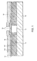
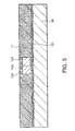
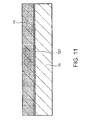
- Fig. 1 is a sectional view showing one example of a structure of a thin film transistor (TFT) according to the present invention, which is applicable to a liquid crystal display device.
- the thin film transistor has a transparent resin film. (insulator layer) 11 formed on a glass substrate (insulating substrate) 10 and formed of a transparent photosensitive resin, and a gate electrode (conductor layer) 12 formed in the transparent resin film 11 so as to reach the glass substrate 10 and formed to a height approximately same as that of the transparent resin film 11.
- the thin film transistor further has a gate insulating film 13 comprising an insulator coating film (overcoat film) 131 formed over the transparent resin film 11 and the gate electrode 12 and a CVD dielectric film (insulator CVD film) 132 formed thereon, a semiconductor layer 14 formed on the gate electrode 12 via the gate insulating film 13, and a source electrode 15 and a drain electrode 16 each of which is connected to the semiconductor layer 14.
- a gate insulating film 13 comprising an insulator coating film (overcoat film) 131 formed over the transparent resin film 11 and the gate electrode 12 and a CVD dielectric film (insulator CVD film) 132 formed thereon, a semiconductor layer 14 formed on the gate electrode 12 via the gate insulating film 13, and a source electrode 15 and a drain electrode 16 each of which is connected to the semiconductor layer 14.
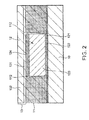
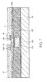
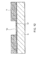
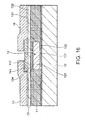
- Fig. 2 is an enlarged sectional view showing a structure of a gate electrode portion of the thin film transistor according to the first embodiment.
- the gate electrode 12 illustrated in the figure is embedded in a trench formed in the flat transparent resin film 11 and comprises, from the side of the glass substrate 10 toward the side of the semiconductor layer (namely, in order from the bottom of the figure), a base adhesive layer 121, a catalyst layer 122, a conductive metal layer 123, and a conductive metal diffusion suppressing layer 124.
- the gate electrode 12 is embedded in the trench of the transparent resin film 11 so that an upper surface of the gate electrode and that of the transparent resin film 11 are approximately flush with each other. Therefore, flatness of an upper structure of the gate electrode 12 is ensured.
- a surface of the conductive metal layer 123 (Cu layer) formed by conventional electroless plating has a flatness up to 17.74 nm in Ra and 193.92 nm in peak-to-valley (P-V) value.
- a surface of the conductive metal diffusion suppressing layer 124 (electroless plated Ni layer) formed thereon also has a flatness of 8.58 nm in Ra and 68.7 nm in peak-to-valley value.
- the insulator coating film 131 having a thickness of 40 nm is formed on the gate electrode 12 and the transparent resin film 11.
- the insulator coating film 131 fills a gap 112 between the gate electrode 12 and the transparent resin film 11 and provides a flat surface which does not reflect asperity of the surface of the gate electrode 12 and which has a flatness of 0.24 nm in Ra and 2.16 nm in peak-to-valley value.
- the above-mentioned values sufficiently satisfy those levels of not greater than 1 nm in Ra and not greater than 20 nm in peak-to-valley value which are required for the insulator coating film, even in case where the surface of the gate electrode has a flatness not smaller than 3 nm in Ra and not smaller than 30 nm in peak-to-valley value.
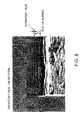
- Fig. 8 is an electron micrograph showing a state, as observed in section by FIB machining, of a structure in which the insulator coating film (overcoat film) is formed on the gate electrode provided by a plated wiring. It is understood that a flat surface is formed independent of roughness of a base as shown in Fig. 8 .
- the silicon nitride dielectric film (CVD dielectric film) 132 formed by CVD on the insulator coating film (overcoat film) 131 and having a thickness of 150 to 160 nm has a surface given a flatness of 0.70 nm in Ra and 7.54 nm in peak-to-valley value ( Fig. 2 ).
- a thin film transistor (TFT) can be formed without causing the asperity deriving from the gate electrode to be produced on the semiconductor layer formed on the gate insulating film 13. Therefore, mobility of a carrier can significantly be improved.
- SOG spin-on glass
- a SOG film is prepared by a siloxane component to be a film, an alcohol component as a solvent, and the like.
- the above-mentioned solution is applied onto the substrate by spin coating and the solvent and the like are evaporated by heat treatment to harden the film. As a result, a SOG insulating film is formed.
- the SOG is an inclusive term used to represent the above-mentioned solution and the film to be formed.
- the SOG is classified into silica glass, an alkyl siloxane polymer, an alkyl silsesquioxane polymer (MSQ), a hydrogen silsesquioxane polymer (HSQ), and a hydrogen alkyl silsesquioxane polymer (HOSQ).
- the silica glass is a first generation inorganic SOG
- the alkyl siloxane polymer is a first generation organic SOG
- the HSQ is a second generation inorganic SOG
- the MSQ and the HOST are a second generation organic SOG.
- baking is often carried out at a temperature not lower than 500 °C.
- a high temperature can not be used when the transparent resin layer is used. Therefore, a material having a baking temperature of not higher than 300 °C is used.
- a material having a baking temperature of not higher than 300 °C is used instead of the Si organic compounds and the Si inorganic compounds mentioned above.
- another metal Ti, Ta, Al, Sn, Zr, and so on are exemplified.
- the thickness is not greater than about 350 to 360 nm and not greater than 200 nm in EOT.
- the EOT is an equivalent silicon dioxide thickness obtained by dividing a dielectric constant of silicon dioxide by an average dielectric constant of a film and then multiplying a quotient by a film thickness.
- the thickness of the gate insulating film is too small, a leak current is increased.
- the voltage of 15V at maximum is applied between a gate and a source of the TFT so that a withstand voltage is preferably not lower than 15V. Therefore, it is preferable that the thickness is not smaller than 95 nm in EOT.
- the insulator coating film 131 is required to have a physical film thickness of at least 40 nm (if a surface roughness of the base is about 30 nm in peak-to-valley value).
- the film may have various dielectric constants, the dielectric constant is about 10 at maximum. Taking this into consideration, it is preferable that the thickness is not smaller than 15 nm in EOT. Furthermore, the maximum film thickness is preferably not greater than about 120 nm.
- the CVD dielectric film 132 preferably has a thickness of not smaller than 80 nm in EOT, considering that the film is mainly responsible for a withstand voltage.
- the insulator coating film 131 has a dielectric constant of not smaller than 2.6, while the CVD dielectric film 132 has a dielectric constant of not less than 4.0.
- Figs. 3 through 7 are schematic diagrams showing, step by step, a method of manufacturing the thin film transistor according to the first embodiment.
- a glass substrate 10 is prepared as a substrate.
- a large-sized substrate adapted to form a large-sized screen of 30 inches or more may be used.
- the glass substrate is treated with a 0.5 vol% aqueous solution of hydrofluoric acid for 10 seconds and washed with pure water to remove surface contamination by liftoff.
- the glass substrate 10 was treated with a silane coupling agent solution which was obtained by preparing an aqueous solution having pH controlled to 10 by adding sodium hydroxide to pure water and then dissolving aminopropylethoxysilane as a silane coupling agent in the aqueous solution at a concentration of 0.1 vol%. Specifically, the glass substrate was dipped into the silane coupling agent solution at a room temperature for 30 minutes to allow the silane coupling agent to be adsorbed onto a surface of the glass substrate. Thereafter, the glass substrate was treated on a hot plate at 110 °C for 60 minutes to chemically bond the silane coupling agent onto the surface of the glass substrate. Thus, the base adhesive layer (10 nm thick) 121 was formed.
- a silane coupling agent solution which was obtained by preparing an aqueous solution having pH controlled to 10 by adding sodium hydroxide to pure water and then dissolving aminopropylethoxysilane as a silane coupling agent in the aqueous solution at a concentration of
- the base adhesive layer 121 By forming the base adhesive layer 121 as mentioned above, an amino group is substantially arranged on the surface of the glass substrate 10. Therefore, a structure which allows easy coordination of a metal complex can be formed.
- the silane coupling agent is generally transparent. Therefore, even if the base adhesive layer is formed throughout the entire surface of the glass substrate 10, an effect of the present invention can be obtained. Furthermore, forming the base adhesive layer is preferable in view of obtaining adhesion between the glass substrate 10 and a transparent photosensitive resin which is used in a subsequent process.
- a positive photoresist solution was applied to a surface of the base adhesive layer 121 by using a spinner. Then, prebaking was performed by heating on a hot plate at 100 °C for 120 seconds. Thus, the photosensitive transparent resin film 11 having a thickness of 2 ⁇ m was formed.
- the positive photoresist mentioned above use was made of a photoresist containing an alkali-soluble alicyclic olefin-based resin described in Patent Document 4 ( JP-A-2002-296780 ).
- a transparent resin selected from a group including an acryl-based resin, a silicone-based resin, a fluorine-based resin, a polyimide-based resin, a polyolefin-based resin, an alicyclic olefin resin, and an epoxy-based resin is usable.
- a photosensitive transparent resin film containing the alkali-soluble alicyclic olefin-based resin and a radiation-sensitive component is advantageous as the transparent film.
- a mixed light of g, h, and i rays was selectively irradiated onto the photosensitive transparent resin film 11 through a mask pattern using a mask aligner. Then, after development for 90 seconds with a 0.3 wt% tetramethylammonium hydroxide aqueous solution, rinsing was carried out with pure water for 60 seconds. In this manner, a trench having a predetermined pattern was formed on the glass substrate 10. Thereafter, a heat treatment was carried out in a nitrogen atmosphere at 230 °C for 60 minutes to thereby harden the photosensitive transparent resin film 11.
- the substrate was dipped into a palladium chloride-hydrochloric acid aqueous solution (0.005 vol% palladium chloride, 0.01 vol% hydrochloric acid) at a room temperature for 3 minutes, treated with a reducing agent (Reducer MAB-2 manufactured by C. Uyemura & Co., Ltd.), and washed with water.
- a reducing agent Reducer MAB-2 manufactured by C. Uyemura & Co., Ltd.
- the substrate provided with the palladium catalyst 122 was dipped into an electroless copper plating solution (PGT manufactured by C. Uyemura & Co., Ltd.) to selectively form the copper layer 123 (conductive metal layer: 1.9 ⁇ m thick) in the trench mentioned above.
- PTT electroless copper plating solution
- formation of the copper layer 123 is finished at a position lower than a height of the surface of the photosensitive transparent resin film 11 by a film thickness of the diffusion suppressing film (conductive metal diffusion suppressing layer) 124 subsequently formed.
- the substrate was dipped into an electroless nickel plating solution to form the diffusion suppressing film 124 (0.1 ⁇ m thick) of nickel on the copper layer 123.
- the conductive metal layer 123 contains at least one of Cu and Ag and that the diffusion suppressing film (conductive metal diffusion suppressing layer) 124 contains a metal selected from Ni, W, Ta, Nb, and Ti.
- the conductive metal layer may be formed by printing, ink-jet, or sputtering, instead of plating.
- Al is suitable as the metal instead of Cu and Ag. If Al is used, the diffusion suppressing film (conductive metal diffusion suppressing layer) may be omitted.
- the insulator coating film 131 was formed so as to extend over the surface of the gate electrode 12 and the surface of the photosensitive transparent resin film 11.
- the insulator coating film 131 is obtained by applying a liquid which is prepared by dissolving organosiloxane as a Si organic compound in an organic solvent (propylene glycol monomethyl ether), keeping at 120 °C in an atmosphere for 90 seconds to dry, and then baking in an atmosphere (may also be in a nitrogen gas) at 180 °C for 1 hour.
- the Si 3 N 4 film (silicon nitride dielectric film) 132 was grown by CVD to form the gate insulating film 13.
- an amorphous silicon film 141 and an n + -type amorphous silicon film 142 were successively deposited by known PECVD (Plasma Enhanced Chemical Vapor Deposition). Then, the amorphous silicon films were partially removed except in an area on the gate electrode 12 and its surrounding area by photolithography or known RIE (Reactive Ion Etching).
- a source electrode and a drain electrode film formation was subsequently carried out in order of Ti, Al, and Ti by known sputtering or the like and patterning was carried out by photolithography. As a result, the source electrode 15 and the drain electrode 16 were formed. Next, using, as a mask, the source electrode 15 and the drain electrode 16 thus formed, the n + -type amorphous silicon film 142 was etched by a known technique to thereby separate a source region and a drain region. Next, by known PECVD, a silicon nitride film (not shown) was formed as a protective film. As a result, the thin film transistor of the first embodiment was completed.
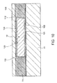
- Fig. 9 is a sectional view showing a structure of a thin film transistor (TFT) according to the second embodiment of the present invention, which is applicable to a liquid crystal display device.
- the thin film transistor comprises a transparent resin film 11 formed on a glass substrate (insulating substrate) 10 and formed of a transparent photosensitive resin, a gate electrode 12 formed in the transparent resin film 11 so as to reach the glass substrate 10 and formed to a height approximately same as that of the transparent resin film 11, a gate insulating film 133 formed over the transparent resin film 11 and the gate electrode 12 and comprising an insulator coating film, a semiconductor layer 14 formed on the gate electrode 12 via the gate insulating film 133, and a source electrode 15 and a drain electrode 16 each of which is connected to the semiconductor layer 14.
- Fig. 10 is an enlarged sectional view showing a structure of a gate electrode portion of the thin film transistor according to the second embodiment.
- the gate electrode 12 illustrated in the figure comprises, from the side of the glass substrate 10 toward the side of the semiconductor layer (namely, in order from the bottom of the figure), a base adhesive layer 121, a catalyst layer 122, a conductive metal layer 123, and a conductive metal diffusion suppressing layer 124.
- the gate electrode 12 is embedded in a trench formed in the flat transparent resin film 11. As shown in the figure, the gate electrode 12 is embedded in the trench of the transparent resin film 11 so that an upper surface of the gate electrode and that of the transparent resin film 11 are approximately flush with each other. Therefore, flatness of an upper structure of the gate electrode 12 is ensured.
- a surface of the conductive metal layer 123 (Cu layer) formed by conventional electroless plating has a flatness up to 17.74 nm in Ra and 193.92 nm in peak-to-valley value.
- a surface of the conductive metal diffusion suppressing layer to (electroless plated Ni layer) formed thereon also has a flatness of 8.58 nm in Ra and 68.7 nm in peak-to-valley value.
- the insulator coating film (gate insulating film) 133 having a thickness of 250 nm is formed on the conductive metal diffusion suppressing layer 124.
- the insulator coating film 133 filled a gap 112 between the gate electrode 12 and the transparent resin film 11 and provided the gate insulating film having a flat surface which did not reflect asperity of the surface of the gate electrode 12 and which had a flatness of 0.30 nm in Ra and 3.55 nm in peak-to-valley value.
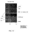
- Fig. 17 is an electron micrograph showing a state, as observed in section, of a structure in which the gate insulating film comprising the insulator coating film is formed on the gate electrode. It is understood that a flat surface is formed independent of roughness of a base as shown in Fig. 17 .
- a thin film transistor can be formed without causing the asperity deriving from the gate electrode 12 to be produced on the semiconductor layer formed on the gate insulating film. Therefore, mobility of a carrier can significantly be improved. Furthermore, in a film forming process of the gate insulating film, a CVD process for forming a CVD dielectric film is omitted and film formation is performed by a simple coating process. Thus, simplification of the process was achieved.
- Figs. 11 through 15 are schematic diagrams showing, step by step, a method of manufacturing the thin film transistor according to the second embodiment.
- the glass substrate 10 is prepared as a substrate.
- a large-sized substrate adapted to form a large-sized screen of 30 inches or more may be used.
- the glass substrate is treated with a 0.5 vol% aqueous solution of hydrofluoric acid for 10 seconds and washed with pure water to remove surface contamination by liftoff.
- the glass substrate 10 was treated with a silane coupling agent solution which was obtained by preparing an aqueous solution having pH controlled to 10 by adding sodium hydroxide to pure water and then dissolving aminopropylethoxysilane as a silane coupling agent in the aqueous solution at a concentration of 0.1 vol%. Specifically, the glass substrate was dipped into the silane coupling agent solution at a room temperature for 30 minutes to allow the silane coupling agent to be adsorbed onto the glass substrate 10. Thereafter, the glass substrate 10 was treated on a hot plate at 110 °C for 60 minutes to chemically bond the silane coupling agent onto the surface of the glass substrate. Thus, the base adhesive layer (10 nm thick) 121 was formed.
- a silane coupling agent solution which was obtained by preparing an aqueous solution having pH controlled to 10 by adding sodium hydroxide to pure water and then dissolving aminopropylethoxysilane as a silane coupling agent in the aqueous solution at a concentration of 0.1 vol
- the base adhesive layer 121 By forming the base adhesive layer 121 as mentioned above, an amino group is substantially arranged on the surface of the substrate. Therefore, a structure which allows easy coordination of a metal complex can be formed.
- the silane coupling agent is generally transparent. Therefore, even if the base adhesive layer is formed throughout the entire surface of the glass substrate 10, an effect of the present invention can be obtained. Furthermore, forming the base adhesive layer is preferable in view of obtaining adhesion between the glass substrate 10 and a transparent photosensitive resin which is used in a subsequent process.
- a positive photoresist solution was applied to a surface of the base adhesive layer 121 by using a spinner. Then, prebaking was performed by heating on a hot plate at 100 °C for 120 seconds. Thus, the photosensitive transparent resin film 11 having a thickness of 2 ⁇ m was formed.
- the positive photoresist mentioned above use was made of a photoresist containing an alkali-soluble alicyclic olefin-based resin described in the publication of Patent Document 4.
- a transparent resin selected from a group including an acryl-based resin, a silicone-based resin, a fluorine-based resin, a polyimide-based resin, a polyolefin-based resin, an alicyclic olefin resin, and an epoxy-based resin is usable.
- a photosensitive transparent resin film is advantageous as the transparent film.
- a mixed light of g, h, and i rays was selectively irradiated onto the photosensitive transparent resin film 11 through a mask pattern using a mask aligner. Then, after development for 90 seconds with a 0.3 wt% tetramethylammonium hydroxide aqueous solution, rinsing was carried out with pure water for 60 seconds. In this manner, a trench having a predetermined pattern was formed on the glass substrate 10. Thereafter, a heat treatment was carried out in a nitrogen atmosphere at 230 °C for 60 minutes to thereby harden the photosensitive transparent resin film 11.
- the substrate was dipped into a palladium chloride-hydrochloric acid aqueous solution (0.005 vol% palladium chloride, 0.01 vol% hydrochloric acid) at a room temperature for 3 minutes, treated with a reducing agent (Reducer MAB-2 manufactured by C. Uyemura & Co., Ltd.), and washed with water.
- a reducing agent Reducer MAB-2 manufactured by C. Uyemura & Co., Ltd.
- the glass substrate 10 provided with the palladium catalyst 122 was dipped into an electroless copper plating solution (PGT manufactured by C. Uyemura & Co., Ltd.) to selectively form the copper layer 123 (1.9 ⁇ m tick) as the conductive metal layer in the trench mentioned above.
- PTT electroless copper plating solution
- formation of the copper layer 123 is finished at a position lower than a height of the surface of the photosensitive transparent resin film 11 by a film thickness of the diffusion suppressing film (conductive metal diffusion suppressing layer) 124 subsequently formed.
- the substrate was dipped into an electroless nickel plating solution to form the diffusion suppressing film 124 (0.1 ⁇ m thick) of nickel on the copper layer 123.
- an insulator film was applied so as to extend over the surface of the gate electrode 12 and the surface of the photosensitive transparent resin film 11 to form the gate insulating film 133.
- the gate insulating film 133 was obtained by applying a liquid which was prepared by dissolving organosiloxane as a Si organic compound in an organic solvent (propylene glycol monomethyl ether), keeping at 120 °C in an atmosphere for 90 seconds to dry, and then baking in an atmosphere (may also be in a nitrogen gas) at 180 °C for 1 hour.
- an amorphous silicon film 141 and an n + -type amorphous silicon film 142 were successively deposited by known PECVD. Then, the amorphous silicon films were partially removed except in an area on the gate electrode 12 and its surrounding area by photolithography or known RIE.
- a source electrode and a drain electrode film formation was subsequently carried out in order of Ti, Al, and Ti by known sputtering or the like and patterning was carried out by photolithography. As a result, the source electrode 15 and the drain electrode 16 were formed. Next, using, as a mask, the source electrode 15 and the drain electrode 16 thus formed, the n + -type amorphous silicon film 142 was etched by a known technique to thereby separate a source region and a drain region. Next, by known PECVD, a silicon nitride film (not shown) was formed as a protective film. As a result, the thin film transistor of the second embodiment was completed.
- FIG. 16 A method of forming a thin film transistor according to a third embodiment and applicable to a liquid crystal display device will be described using Fig. 16 .
- the diffusion suppressing film 124 (0.1 ⁇ m thick) of nickel was formed on the copper layer 123 to form the gate electrode 12.
- the Si 3 N 4 film (silicon nitride dielectric film) 132 was grown by CVD using a microwave excited RLSA plasma processing device to form an insulating film.
- the insulator coating film 131 was applied and formed over the Si 3 N 4 film 132 throughout its entirety. As a result, the gate insulating film 13 was formed.
- the insulator coating film 131 was obtained by applying a liquid which was prepared by dissolving organosiloxane as a Si organic compound in an organic solvent (propylene glycol monomethyl ether), keeping at 120 °C in an atmosphere for 90 seconds to dry, and then baking in an atmosphere (may also be in a nitrogen gas) at 180 °C for 1 hour.
- an atmosphere may also be in a nitrogen gas
- a material other than copper and silver may also be used.
- a conductive film of metal oxide such as indium-tin oxide (ITO) may be formed.
- the present invention is applicable to a display device, such as a liquid crystal display device, an organic EL device, and an inorganic EL device, and makes it possible to increase the size of these display devices. Furthermore, the present invention is applicable also to a wiring other than the display devices.
Landscapes
- Engineering & Computer Science (AREA)
- Microelectronics & Electronic Packaging (AREA)
- Power Engineering (AREA)
- Condensed Matter Physics & Semiconductors (AREA)
- General Physics & Mathematics (AREA)
- Physics & Mathematics (AREA)
- Computer Hardware Design (AREA)
- Ceramic Engineering (AREA)
- Manufacturing & Machinery (AREA)
- Chemical & Material Sciences (AREA)
- Chemical Kinetics & Catalysis (AREA)
- Thin Film Transistor (AREA)
- Electrodes Of Semiconductors (AREA)
Applications Claiming Priority (3)
| Application Number | Priority Date | Filing Date | Title |
|---|---|---|---|
| JP2006257848 | 2006-09-22 | ||
| JP2006313492A JP2008103653A (ja) | 2006-09-22 | 2006-11-20 | 半導体装置及び半導体装置の製造方法 |
| PCT/JP2007/068458 WO2008035786A1 (fr) | 2006-09-22 | 2007-09-21 | Dispositif semi-conducteur et procédé de fabrication d'un dispositif semi-conducteur |
Publications (1)
| Publication Number | Publication Date |
|---|---|
| EP2088629A1 true EP2088629A1 (en) | 2009-08-12 |
Family
ID=39200608
Family Applications (1)
| Application Number | Title | Priority Date | Filing Date |
|---|---|---|---|
| EP07807788A Withdrawn EP2088629A1 (en) | 2006-09-22 | 2007-09-21 | Semiconductor device and semiconductor device manufacturing method |
Country Status (6)
| Country | Link |
|---|---|
| US (1) | US20090278134A1 (ja) |
| EP (1) | EP2088629A1 (ja) |
| JP (1) | JP2008103653A (ja) |
| KR (1) | KR20090071538A (ja) |
| TW (1) | TW200832718A (ja) |
| WO (1) | WO2008035786A1 (ja) |
Cited By (2)
| Publication number | Priority date | Publication date | Assignee | Title |
|---|---|---|---|---|
| US10134909B2 (en) | 2012-05-31 | 2018-11-20 | Semiconductor Energy Laboratory Co., Ltd. | Semiconductor device and method for manufacturing the same |
| US11282964B2 (en) | 2017-12-07 | 2022-03-22 | Semiconductor Energy Laboratory Co., Ltd. | Semiconductor device |
Families Citing this family (6)
| Publication number | Priority date | Publication date | Assignee | Title |
|---|---|---|---|---|
| CN101807004B (zh) * | 2010-03-08 | 2012-07-11 | 彩虹集团电子股份有限公司 | 一种用于彩色显像管网版生产的工作版的制做方法 |
| US9087749B2 (en) * | 2010-12-27 | 2015-07-21 | Sharp Kabushiki Kaisha | Active matrix substrate, and display panel |
| US8987071B2 (en) * | 2011-12-21 | 2015-03-24 | National Applied Research Laboratories | Thin film transistor and fabricating method |
| CN103681870B (zh) * | 2012-09-13 | 2016-12-21 | 北京京东方光电科技有限公司 | 阵列基板及其制造方法 |
| WO2015076358A1 (ja) | 2013-11-21 | 2015-05-28 | 株式会社ニコン | 配線パターンの製造方法およびトランジスタの製造方法 |
| JP6926939B2 (ja) * | 2017-10-23 | 2021-08-25 | 東京エレクトロン株式会社 | 半導体装置の製造方法 |
Family Cites Families (18)
| Publication number | Priority date | Publication date | Assignee | Title |
|---|---|---|---|---|
| JPH0812539B2 (ja) * | 1985-01-29 | 1996-02-07 | 株式会社東芝 | 表示装置及びその製造方法 |
| JPH03159174A (ja) * | 1989-11-16 | 1991-07-09 | Sanyo Electric Co Ltd | 液晶表示装置 |
| JP3173926B2 (ja) * | 1993-08-12 | 2001-06-04 | 株式会社半導体エネルギー研究所 | 薄膜状絶縁ゲイト型半導体装置の作製方法及びその半導体装置 |
| JPH10268343A (ja) * | 1997-03-24 | 1998-10-09 | Sharp Corp | 液晶表示装置およびその製造方法 |
| JP2001188343A (ja) | 1999-12-28 | 2001-07-10 | Nippon Zeon Co Ltd | 感光性樹脂組成物 |
| EP1369928B1 (en) * | 2001-02-19 | 2010-01-27 | International Business Machines Corporation | Method for manufacturing a thin-film transistor structure |
| JP2002296780A (ja) | 2001-03-30 | 2002-10-09 | Nippon Zeon Co Ltd | 感光性樹脂組成物 |
| JP2002353167A (ja) * | 2001-05-29 | 2002-12-06 | Sharp Corp | 金属配線基板及び金属配線基板の製造方法並びに反射型液晶表示装置用金属配線基板 |
| US6835503B2 (en) * | 2002-04-12 | 2004-12-28 | Micron Technology, Inc. | Use of a planarizing layer to improve multilayer performance in extreme ultra-violet masks |
| JP2003318401A (ja) * | 2002-04-22 | 2003-11-07 | Seiko Epson Corp | デバイスの製造方法、デバイス、表示装置、および電子機器 |
| CN1799292B (zh) | 2003-06-04 | 2012-02-08 | 日本瑞翁株式会社 | 基板制造方法 |
| US6969634B2 (en) * | 2003-09-24 | 2005-11-29 | Lucent Technologies Inc. | Semiconductor layers with roughness patterning |
| JP4554344B2 (ja) | 2003-12-02 | 2010-09-29 | 株式会社半導体エネルギー研究所 | 半導体装置の作製方法 |
| JP4286116B2 (ja) | 2003-12-09 | 2009-06-24 | 株式会社リコー | 画像形成用トナー、現像剤及び画像形成装置 |
| JPWO2005096684A1 (ja) * | 2004-03-31 | 2008-02-21 | 大見 忠弘 | 回路基板、回路基板の製造方法及び回路基板を備えた表示装置 |
| US7864398B2 (en) * | 2004-06-08 | 2011-01-04 | Gentex Corporation | Electro-optical element including metallic films and methods for applying the same |
| JP4543385B2 (ja) * | 2005-03-15 | 2010-09-15 | 日本電気株式会社 | 液晶表示装置の製造方法 |
| US7919825B2 (en) * | 2006-06-02 | 2011-04-05 | Air Products And Chemicals, Inc. | Thin film transistors with poly(arylene ether) polymers as gate dielectrics and passivation layers |
-
2006
- 2006-11-20 JP JP2006313492A patent/JP2008103653A/ja not_active Withdrawn
-
2007
- 2007-09-21 US US12/442,330 patent/US20090278134A1/en not_active Abandoned
- 2007-09-21 EP EP07807788A patent/EP2088629A1/en not_active Withdrawn
- 2007-09-21 KR KR1020097002202A patent/KR20090071538A/ko not_active Application Discontinuation
- 2007-09-21 WO PCT/JP2007/068458 patent/WO2008035786A1/ja active Application Filing
- 2007-09-26 TW TW096135728A patent/TW200832718A/zh unknown
Non-Patent Citations (1)
| Title |
|---|
| See references of WO2008035786A1 * |
Cited By (3)
| Publication number | Priority date | Publication date | Assignee | Title |
|---|---|---|---|---|
| US10134909B2 (en) | 2012-05-31 | 2018-11-20 | Semiconductor Energy Laboratory Co., Ltd. | Semiconductor device and method for manufacturing the same |
| US11282964B2 (en) | 2017-12-07 | 2022-03-22 | Semiconductor Energy Laboratory Co., Ltd. | Semiconductor device |
| US11784259B2 (en) | 2017-12-07 | 2023-10-10 | Semiconductor Energy Laboratory Co., Ltd. | Oxide semiconductor device |
Also Published As
| Publication number | Publication date |
|---|---|
| KR20090071538A (ko) | 2009-07-01 |
| TW200832718A (en) | 2008-08-01 |
| JP2008103653A (ja) | 2008-05-01 |
| WO2008035786A1 (fr) | 2008-03-27 |
| US20090278134A1 (en) | 2009-11-12 |
Similar Documents
| Publication | Publication Date | Title |
|---|---|---|
| EP2088629A1 (en) | Semiconductor device and semiconductor device manufacturing method | |
| US6887776B2 (en) | Methods to form metal lines using selective electrochemical deposition | |
| KR100711526B1 (ko) | 구리 연결선을 갖는 반도체 장치의 제조방법 | |
| KR101004219B1 (ko) | 배선, 배선의 형성방법, 박막 트랜지스터 및 표시장치 | |
| US6492269B1 (en) | Methods for edge alignment mark protection during damascene electrochemical plating of copper | |
| EP2096678A1 (en) | Semiconductor device and method for manufacturing semiconductor device | |
| CN101506985A (zh) | 半导体装置和半导体装置的制造方法 | |
| CN101286473B (zh) | 半导体器件的制造方法 | |
| US6211050B1 (en) | Fill pattern in kerf areas to prevent localized non-uniformities of insulating layers at die corners on semiconductor substrates | |
| CN113764337B (zh) | 导电插塞的制造方法及半导体结构 | |
| CN1270388C (zh) | 薄膜晶体管阵列面板及其制造方法 | |
| JP3393845B2 (ja) | デュアル・ダマシン法のためのシルセスキオキサン誘電体の一時酸化 | |
| US7101788B2 (en) | Semiconductor devices and methods of manufacturing such semiconductor devices | |
| CN102709329A (zh) | 薄膜晶体管及其制造方法 | |
| JP3396790B2 (ja) | 半導体装置及びその製造方法 | |
| US20070049008A1 (en) | Method for forming a capping layer on a semiconductor device | |
| JP2001274191A (ja) | 半導体装置及び半導体装置の製造方法 | |
| WO2016150075A1 (zh) | 薄膜晶体管、薄膜晶体管的制备方法及阵列基板 | |
| CN112864003B (zh) | 降低表面缺陷影响的刻蚀方法 | |
| EP2018662A2 (en) | Power mosfet contact metallization | |
| CN101140899A (zh) | 湿法制作金属导线的方法 | |
| US20080057202A1 (en) | Method of fabricating metal line by wet process | |
| JP2001176872A (ja) | 半導体装置の製造方法 | |
| TW396525B (en) | Method for forming contact windows | |
| KR100214067B1 (ko) | 반도체 장치의 다층금속배선 형성방법 |
Legal Events
| Date | Code | Title | Description |
|---|---|---|---|
| PUAI | Public reference made under article 153(3) epc to a published international application that has entered the european phase |
Free format text: ORIGINAL CODE: 0009012 |
|
| 17P | Request for examination filed |
Effective date: 20090331 |
|
| AK | Designated contracting states |
Kind code of ref document: A1 Designated state(s): AT BE BG CH CY CZ DE DK EE ES FI FR GB GR HU IE IS IT LI LT LU LV MC MT NL PL PT RO SE SI SK TR |
|
| AX | Request for extension of the european patent |
Extension state: AL BA HR MK RS |
|
| DAX | Request for extension of the european patent (deleted) | ||
| RBV | Designated contracting states (corrected) |
Designated state(s): DE FR GB IT NL |
|
| RAP1 | Party data changed (applicant data changed or rights of an application transferred) |
Owner name: ZEON CORPORATION |
|
| STAA | Information on the status of an ep patent application or granted ep patent |
Free format text: STATUS: THE APPLICATION HAS BEEN WITHDRAWN |
|
| 18W | Application withdrawn |
Effective date: 20110620 |