EP2077489B1 - Dispositif de détection de position - Google Patents
Dispositif de détection de position Download PDFInfo
- Publication number
- EP2077489B1 EP2077489B1 EP08022437.1A EP08022437A EP2077489B1 EP 2077489 B1 EP2077489 B1 EP 2077489B1 EP 08022437 A EP08022437 A EP 08022437A EP 2077489 B1 EP2077489 B1 EP 2077489B1
- Authority
- EP
- European Patent Office
- Prior art keywords
- detection
- detection electrode
- section
- electrodes
- detecting device
- Prior art date
- Legal status (The legal status is an assumption and is not a legal conclusion. Google has not performed a legal analysis and makes no representation as to the accuracy of the status listed.)
- Active
Links
Images


Classifications
-
- G—PHYSICS
- G06—COMPUTING; CALCULATING OR COUNTING
- G06F—ELECTRIC DIGITAL DATA PROCESSING
- G06F3/00—Input arrangements for transferring data to be processed into a form capable of being handled by the computer; Output arrangements for transferring data from processing unit to output unit, e.g. interface arrangements
- G06F3/01—Input arrangements or combined input and output arrangements for interaction between user and computer
- G06F3/03—Arrangements for converting the position or the displacement of a member into a coded form
- G06F3/033—Pointing devices displaced or positioned by the user, e.g. mice, trackballs, pens or joysticks; Accessories therefor
- G06F3/0354—Pointing devices displaced or positioned by the user, e.g. mice, trackballs, pens or joysticks; Accessories therefor with detection of 2D relative movements between the device, or an operating part thereof, and a plane or surface, e.g. 2D mice, trackballs, pens or pucks
- G06F3/03545—Pens or stylus
-
- G—PHYSICS
- G06—COMPUTING; CALCULATING OR COUNTING
- G06F—ELECTRIC DIGITAL DATA PROCESSING
- G06F3/00—Input arrangements for transferring data to be processed into a form capable of being handled by the computer; Output arrangements for transferring data from processing unit to output unit, e.g. interface arrangements
- G06F3/01—Input arrangements or combined input and output arrangements for interaction between user and computer
- G06F3/03—Arrangements for converting the position or the displacement of a member into a coded form
- G06F3/041—Digitisers, e.g. for touch screens or touch pads, characterised by the transducing means
- G06F3/044—Digitisers, e.g. for touch screens or touch pads, characterised by the transducing means by capacitive means
- G06F3/0448—Details of the electrode shape, e.g. for enhancing the detection of touches, for generating specific electric field shapes, for enhancing display quality
-
- G—PHYSICS
- G06—COMPUTING; CALCULATING OR COUNTING
- G06F—ELECTRIC DIGITAL DATA PROCESSING
- G06F3/00—Input arrangements for transferring data to be processed into a form capable of being handled by the computer; Output arrangements for transferring data from processing unit to output unit, e.g. interface arrangements
- G06F3/01—Input arrangements or combined input and output arrangements for interaction between user and computer
- G06F3/03—Arrangements for converting the position or the displacement of a member into a coded form
- G06F3/041—Digitisers, e.g. for touch screens or touch pads, characterised by the transducing means
- G06F3/044—Digitisers, e.g. for touch screens or touch pads, characterised by the transducing means by capacitive means
- G06F3/0446—Digitisers, e.g. for touch screens or touch pads, characterised by the transducing means by capacitive means using a grid-like structure of electrodes in at least two directions, e.g. using row and column electrodes
-
- G—PHYSICS
- G06—COMPUTING; CALCULATING OR COUNTING
- G06F—ELECTRIC DIGITAL DATA PROCESSING
- G06F3/00—Input arrangements for transferring data to be processed into a form capable of being handled by the computer; Output arrangements for transferring data from processing unit to output unit, e.g. interface arrangements
- G06F3/01—Input arrangements or combined input and output arrangements for interaction between user and computer
- G06F3/03—Arrangements for converting the position or the displacement of a member into a coded form
- G06F3/041—Digitisers, e.g. for touch screens or touch pads, characterised by the transducing means
- G06F3/046—Digitisers, e.g. for touch screens or touch pads, characterised by the transducing means by electromagnetic means
-
- G—PHYSICS
- G06—COMPUTING; CALCULATING OR COUNTING
- G06F—ELECTRIC DIGITAL DATA PROCESSING
- G06F2203/00—Indexing scheme relating to G06F3/00 - G06F3/048
- G06F2203/041—Indexing scheme relating to G06F3/041 - G06F3/045
- G06F2203/04111—Cross over in capacitive digitiser, i.e. details of structures for connecting electrodes of the sensing pattern where the connections cross each other, e.g. bridge structures comprising an insulating layer, or vias through substrate
Definitions
- the present invention relates to a position detecting device in which an electrostatic capacity type detection section and an electromagnetic induction type detection section are superimposed on each other, so that a position indicated by either a position indicator or a human body part (e.g., a finger) can be detected.
- a position detecting device has been used as a device for performing position input in an information-processing device such as a personal computer.
- a pointing operation or a handwriting input operation such as handwriting a character or hand-drawing an illustration is performed with an input tool such as a pen-like position indicator or a human body part (e.g., a finger).
- Input operation using the position indicator as the input tool is performed based on, for example, an electromagnetic resonance technology, in which the position indicator is provided with a resonant circuit that resonates with an electromagnetic wave of a specified frequency transmitted from the position detecting device. Further, a resonance signal induced in the resonant circuit is transmitted to the position detecting device, so that the position indicator indicates its own position to the position detecting device (see, for example, Japanese Unexamined Patent Application Publication No. 7-302153 ).
- Document DE 20 2007 007 345 U1 relates to a two dimensional position detector shown in figure 2 thereof. Electrodes 14, 16, 18, 20, 22, and 24 are arranged so as to form slits in between those electrodes.
- Document US 5 463 388 A relates to a computer input device for use as a computer mouse or keyboard comprising a thin, insulating surface covering an array of electrodes. Such electrodes are arranged in a grid pattern and can be connected in columns and rows. Each column and row is connected to circuitry for measuring the capacitance seen by each column and row. The position of an object, such as a finger or handheld stylus, with respect to the array is determined from the centroid of such capacitance values, which is calculated in a microcontroller. For applications in which the input device is used as a mouse, the microcontroller forwards position change information to the computer. For applications in which the input device is used as a keyboard, the microcomputer identifies a key from the position of the touching object and forwards such key identity to the computer.
- Document WO 2007/129085 A relates to a navigation arrangement for an electronic device that includes a screen, comprising: (i) a substantially transparent two dimensional capacitive position sensor that can be located over a screen of the device, and which can detect the position of an object with respect to the screen, and (ii) a two dimensional inductive position sensor for detecting the position of an intermediate coupler for example in the form of a pen or stylus with respect to the screen.
- the inductive position sensor comprises a transmit aerial for transmitting a signal, and a receive aerial for receiving the signal via the intermediate coupler so that the position of the intermediate coupler can be determined-
- the wiring of the inductive position sensor may be formed from a transparent conductor, or it may be arranged around the edge of the screen or behind the screen to enable the user to view the screen. Further forms of inductive position sensor, with or without capacitive position sensors, can enable a user to view a screen, for example by placing the inductive sensor tracks around the screen, or by connecting transparent conductors in parallel using low resistance busbars at the edge of the screen. Inductive position sensors may also be arranged to determine the position of the intermediate coupler in three directions, optionally in combination with other forms of sensor, and also to determine its orientation.
- Document US 4 733 222 A relates to a capacitance-variation-sensitive touch sensing array system including an array of electrodes where each electrode is a connected series of conductive tabs and forms either a row or a column of the electrode array; an array of drive lines where each drive line is capacitively coupled to a plurality of the electrodes; a drive signal generator for applying alternating signal packets to the drive lines; an array of sense lines where each sense line is capacitively coupled to a plurality of the electrodes so that signals are derived from the electrodes when drive signals are applied to the drive lines.
- the number of electrodes is equal to the product of the number of drive lines and the number of sense lines.
- a microprocessor Based on values derived from signals on the sense lines, a microprocessor provides information associated with touch by an operator.
- the array of electrodes may be configured so as to result in a touch-actuated keyboard where the number of keys is equal to the product of the number of row electrodes and the number of column electrodes; or the array of electrodes may be configured so that finger touch position in a single large touch responsive area can be sensed and processed for use in control applications.
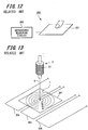
- FIG. 12 is a view schematically showing an electrostatic capacity type detection section 200.
- the detection section 200 includes a flat plate-shaped detection electrode 201 and a capacitance measuring circuit 202.
- a capacitance is generated between the human body part and the detection electrode 201.
- the position where the human body part approaches or contacts with is detected as the position of the detection electrode 201 whose capacitance changes due to the change of the capacitance between the human body part and the detection electrode 201.
- the higher the capacitance between the human body part and the detection electrode 201 the easier the capacitance can be detected.
- a flat electrode having an area at or above a predetermined size is used as the detection electrode 201.
- the electromagnetic induction type detection section since the electromagnetic induction type detection section has high position detecting accuracy compared to the electrostatic capacity type detection section, the electromagnetic induction type detection section is used in a computer, for example, for performing fine input operation such as handwriting a character or hand-drawing an illustration.
- the electrostatic capacity type detection section has low position detecting accuracy compared to the electromagnetic induction type detection section, it can detect an input operation performed by the human body part. Therefore, electrostatic capacity type detection section is used in a device such as a automated teller machine (ATM), a cell-phone or the like, in which input operation is performed by directly touching a screen of the device.
- ATM automated teller machine
- a newer type of position detecting device has been proposed in which both the electromagnetic induction type detection section and the electrostatic capacity type detection section are effectively utilized.
- FIG. 13 is a view schematically showing a position detecting device, in which a detection electrode 201 that constitutes the electrostatic capacity type detection section is disposed above loop coils 304 that constitute the electromagnetic induction type detection section.
- a magnetic flux G generated by a coil 27 of a position indicator 2 is perpendicular to the detection electrode 201 of the electrostatic capacity type detection section.
- the magnetic flux G generates an eddy current I in the detection electrode 201.
- the eddy current I in the detection electrode 201 generates a new magnetic flux which has a direction so as to attenuate the magnetic flux G generated by the position indicator 2 (i.e., the direction of the new magnetic flux is opposite to the direction of the magnetic flux G). Since the new magnetic flux attenuates the magnetic flux G from the position indicator 2, detection of the magnetic flux G by the electromagnetic induction type detection section is reduced. As a result, detection accuracy is lowered.
- the area of the detection electrode be reduced so as to reduce the eddy current generated in the detection electrode.
- the detection accuracy of the electrostatic capacity type detection section will be degraded since the capacitance between a human body part (e.g., a finger) and the detection electrode becomes small.
- the first detection section e.g., an electrostatic capacity type detection section
- the second detection section e.g., an electromagnetic induction type detection section
- a position detecting device includes an electrostatic capacity type detection section according to the claims.
- the position detecting device by forming at least one slit in the detection electrode of the first detection section (an electrostatic capacity type detection section), the eddy current generated in the detection electrode can be prevented or suppressed. Thereby the degradation of the detection accuracy of the second detection section (an electromagnetic induction type detection section) can be prevented or suppressed.
- FIGS. 1 to 11 Embodiments of a position detecting device according to the present invention will be described below with reference to FIGS. 1 to 11 .
- like components are denoted by like numerals. While illustrative embodiments will be illustrated and described, it will be appreciated that various changes can be made therein.
- the position detecting device 1 is connected to an external device (not shown) such as a personal computer, a PDA (Personal Digital Assistant) or the like through a cable 10.
- an external device such as a personal computer, a PDA (Personal Digital Assistant) or the like
- the position detecting device 1 is used as an input device of the external device.
- the position detecting device 1 may also be incorporated into a personal computer or the like.
- the position detecting device 1 includes a first detection section 13, such as an electrostatic capacity type detection section, and a second detection section 14, such as an electromagnetic induction type detection section, which will be described later. Further, a pointing operation or handwriting input operation such as handwriting character or illustration can be performed on the position detecting device 1 with a position indicator 2 or by a human body part (e.g., a finger).
- a first detection section 13 such as an electrostatic capacity type detection section
- a second detection section 14 such as an electromagnetic induction type detection section, which will be described later.
- a pointing operation or handwriting input operation such as handwriting character or illustration can be performed on the position detecting device 1 with a position indicator 2 or by a human body part (e.g., a finger).
- the position indicator 2 indicates its own position to the position detecting device 1 based on electromagnetic resonance technology.
- the position indicator 2 includes a resonant circuit configured by a coil and a capacitor, the resonant circuit resonating with an electromagnetic wave of a specified frequency transmitted from the position detecting device 1.
- a resonance signal induced in the resonant circuit is transmitted to the position detecting device 1, so that the position indicator 2 indicates its own position to the position detecting device 1.
- the position detecting device 1 includes an input section 4 to which information is inputted, and a thin rectangular parallelepiped-shaped housing 5 with the input section 4 fitted therein.
- the housing 5 includes an upper housing 7 having a quadrangular shaped opening 6 formed therein for exposing an input surface of the input section 4, and a lower housing (not shown) coupled with the upper housing 7.
- the input section 4 is fitted into the opening 6.
- the position detecting device 1 includes the input section 4, a capacitance measuring circuit 22, an electromagnetic induction detection circuit 23, and a processing circuit 25.
- the input section 4 includes an insulating cover 12, the first detection section 13, such as an electrostatic capacity type detection section, and the second detection section 14, such as an electromagnetic induction type detection section.
- the first detection section 13 is adapted to detect an approach or contact of the human body part or the like so as to detect the coordinates of a point where the human body part or the like approaches or contacts with the input section 4.
- the second detection section 14 is adapted to detect the coordinates of an approach or contact by the position indicator 2 on the input section 4.
- the capacitance measuring circuit 22 is adapted to measure the change of the capacitance of detection electrodes provided in the first detection section 13, and is connected to the first detection section 13 and the processing circuit 25.
- the electromagnetic induction detection circuit 23 is adapted to detect the position (for example, by coordinates) of the point indicated by the position indicator 2, and is connected to the second detection section 14 and the processing circuit 25.
- the processing circuit 25 is adapted to calculate coordinate data of the point indicated by the human body part or the position indicator 2 and detected by the capacitance measuring circuit 22 or electromagnetic induction detection circuit 23.
- the processing circuit 25 outputs the calculated coordinate data to an external device (not shown) such as a personal computer or a PDA, or to a central processing unit (CPU) of a personal computer or the like. It will be recognized that the position detecting device 1 may be incorporated in the personal computer or the PDA, or the like.
- the input section 4 is formed in a thin flat shape.
- the input section 4 is configured by the insulating cover 12, the first detection section 13 having a substantially rectangular detection area 16 arranged on one surface thereof, and the second detection section 14 provided with a plurality of loop coils 24. Further, in the input section 4, the cover 12 and the first detection section 13 are arranged so that one surface of the cover 12 faces the one surface of the first detection section 13. The second detection section 14 is arranged so as to face the other surface of the first detection section 13. Thus, in the input section 4, the cover 12, the first detection section 13 and the second detection section 14 are superimposed on each other.
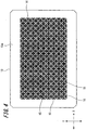
- the first detection section 13 is configured by a substantially rectangular substrate 13a, and the substantially rectangular detection area 16 formed in substantially the central portion of one surface (referred to as "front surface” hereinafter) of the substrate 13a.
- the detection area 16 is adapted to detect an approach or contact of the human body part or the like so as to detect the coordinates of a point where the human body part or the like approaches or contacts with the input section 4.
- the detection area 16 is configured by a plurality of detection electrodes 15.
- the detection electrodes 15 arranged in an outer peripheral portion of the detection area 16 are each formed in a substantially triangular shape, and the detection electrodes 15 arranged in an inner portion of the detection area 16 are each formed in a substantially quadrangular shape.
- the detection area 16 is configured by a first detection electrode group 16A and a second detection electrode group 16B.
- the first detection electrode group 16A is configured by a plurality of first detection electrode arrays 15a arranged in parallel with a short-side direction (referred to as Y-axis direction hereinafter) of the substrate 13a, each first detection electrode array 15a being formed by connecting a plurality of detection electrodes 15 at a predetermined interval.
- the first detection electrode group 16A is formed by arranging the plurality of first detection electrode arrays 15a in a long-side direction (referred to as X-axis direction hereinafter) perpendicular to the Y-axis direction of the substrate 13a at a predetermined interval.
- the detection electrodes 15 adjacent in the Y-axis direction are electrically connected to each other by connecting the respective vertexes thereof with connecting portions 18a.
- the second detection electrode group 16B is configured by a plurality of second detection electrode arrays 15b arranged in the X-axis direction of the substrate 13a, each second detection electrode array 15b being formed by connecting a plurality of detection electrodes 15 at a predetermined interval.
- the second detection electrode group 16B is formed by arranging the plurality of second detection electrode arrays 15b in the Y-axis direction of the substrate 13a at a predetermined interval.
- the detection electrodes 15 adjacent in the X-axis direction are electrically connected to each other by connecting the respective vertexes thereof with connecting portions 18b.
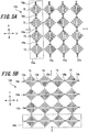
- the detection area 16 is formed such that the gaps between the detection electrodes 15 of the first detection electrode groups 16A as seen in FIG. 5A , and the gaps between the detection electrodes 15 of the second detection electrode group 16B as seen in FIG. 5B , are respectively filled by the second detection electrode group 16B and the first detection electrode group 16A. Since the gaps between the detection electrodes 15 of the first detection electrode groups 16A and the gaps between the detection electrodes 15 of the second detection electrode group 16B are filled, when the human body part approaches the first detection section 13, the human body part faces the detection electrodes 15 of both the first and second detection electrode groups 16A, 16B.
- the connecting portions 18a of the first detection electrode arrays 15a as seen in FIG. 5A connect the adjacent detection electrodes 15 on the other surface (referred to as "rear surface” hereinafter) side of the first detection section 13.
- the connecting portion 18b of the second detection electrode arrays 15b as seen in FIG. 5B connect the adjacent detection electrodes 15 on the front surface side of the first detection section 13.
- a plurality of lead wires 17 are provided on the rear surface of the first detection section 13.
- the first detection electrode group 16A and the second detection electrode group 16B are connected to the capacitance measuring circuit 22 through the lead wires 17.
- the size of each of the detection electrodes 15 is set so that when the human body part approaches or contacts with the input section 4, the human body part faces at least two detection electrodes 15 of the first detection electrode group 16A and two detection electrodes 15 of the second detection electrode group 16B.
- the human body part faces at least two detection electrodes 15 in both the X-axis direction and Y-axis direction, the position where the human body part approaches or contacts with the input section 4 can be detected more precisely based on a capacitance difference between the two detection electrodes 15.
- the detection electrode 15 may be formed in a substantially quadrangular shape (the detection electrode 15 arranged in the outer peripheral portion of the detection area 16 may be formed in a substantially triangular shape), and may be formed with a plurality of slits 19.
- the plurality of slits 19 are arranged in parallel with each other at substantially equal intervals. Further, the plurality of slits 19 are arranged in line-symmetry by using a line connecting two vertexes (to which the connecting portions 18a and 18b are connected) as a symmetry axis, so that six slits 19, for example, are formed on each side.
- each of the slits 19 extends from the outer edge to the inner side of the detection electrode 15, and is open at the outer edge of the detection electrode 15 and closed at the inner side of the detection electrode 15.
- the detection electrode 15 as a whole has a comb shape.
- the slits 19 may be formed by etching the detection electrode 15.
- the length of the diagonal connecting two opposite vertexes is set to, for example, 5 mm, and the width of each of the slits 19 is set to, for example, 0.1 mm.
- the opening area of the slit 19 is small enough compared to the area of the detection electrode 15.
- the area of the detection electrode 15 having slits 19 is almost equal to the area of a conventional detection electrode having no slit.
- the detection accuracy of the first detection section 13, such as an electrostatic capacity type detection section, according to the present embodiment is almost the same as that of a conventional detection electrode having no slit.
- the present embodiment is described using an example in which the detection electrode 15 is formed in a substantially quadrangular shape, the present invention is not limited thereto.
- the detection electrode can be formed in a hexagonal shape or a circular shape.
- a plurality of detection electrodes are arranged in a honeycomb shape.
- the number of the slits 19 formed on each side of the symmetry axis may be five, seven, less than five, or more than seven.
- the slits 19 are formed by etching in the present embodiment, the method for forming the slits 19 is not limited to etching.
- the slits 19 may be formed by printing a silver paste, or the like, on the substrate 13a using an ink jet printer.
- a predetermined voltage from the capacitance measuring circuit 22 is applied to the plurality of detection electrodes 15 forming the first detection section 13. Further, when the human body part approaches or contacts with the input section 4, the capacitance between the human body part and the detection electrode 15 being approached will change since the human body part is considered a grounding body.
- the capacitance measuring circuit 22 identifies the detection electrodes 15 whose capacitance changes, and executes an arithmetic processing based on the position and capacitance change of the identified detection electrode 15 and the like to detect the position where the human body part approaches or contacts with the input section 4.
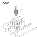
- the second detection section 14 is provided with a plurality of loop coils 24 on its surface opposing the rear surface of the first detection section 13, and the plurality of loop coils 24 are connected to the electromagnetic induction detection circuit 23.
- the second detection section 14 has forty loop coils 24X 1 -24X 40 arranged in the X-axis direction, and forty loop coils 24Y 1 -24Y 40 arranged in the Y-axis direction.
- the loop coils 24X 1 -24X 40 and loop coils 24Y 1 -24Y 40 are connected to a selecting circuit 106 of the electromagnetic induction detection circuit 23, the selecting circuit 106 being adapted to select each of the loop coils 24.
- the number of the loop coils 24 is forty in each direction in the present embodiment, the number of the loop coils 24 is not limited to forty.
- the electromagnetic induction detection circuit 23 includes the selecting circuit 106, a transmission/reception switching circuit 107, an amplifier 108, a detection circuit 109, a low-pass filter (LPF) 110, and a sample-and-hold circuit 112.
- the selecting circuit 106 is connected to the transmission/reception switching circuit 107, and the amplifier 108 is connected to a reception side of the transmission/reception switching circuit 107.
- the amplifier 108 is connected to the detection circuit 109, and the detection circuit 109 is connected to the sample-and-hold circuit 112 through the low-pass filter (LPF) 110.
- sample-and-hold circuit 112 is connected to an A/D conversion circuit (analog-digital conversion circuit) 113, and the A/D conversion circuit 113 is connected to a CPU (central processing unit) 114.
- the CPU 114 supplies control signals to the selecting circuit 106, the sample-and-hold circuit 112, the A/D conversion circuit 113 and the transmission/reception switching circuit 107.
- the electromagnetic induction detection circuit 23 is provided with an oscillator 116 for generating an AC signal having a frequency f 0 and a current driver 117 for converting the AC signal to a current, the current driver 117 being connected to a transmission side of the transmission/reception switching circuit 107.
- an oscillator 116 for generating an AC signal having a frequency f 0
- a current driver 117 for converting the AC signal to a current
- the current driver 117 being connected to a transmission side of the transmission/reception switching circuit 107.
- the resonant circuit incorporated into the position indicator 2 will resonate so as to generate an induced voltage. Then, in the second detection section 14 of the input section 4, when the contact point of the transmission/reception switching circuit 107 is switched to the reception side in response to the control signal supplied from the CPU 114, the supply of the magnetic field to the position indicator 2 is stopped. Thus, due to the induced voltage previously generated during reception time, a magnetic field is generated by the coil incorporated in the position indicator 2. The second detection section 14 detects the position of the position indicator 2 by detecting the magnetic field generated by the coil incorporated in the position indicator 2.
- the switching of the detection method of the input section 4 is not limited to the above-mentioned manner.
- a change-over switch may be provided to allow the user to optionally switch the detection method of the input section 4 between the first detection section 13 and the second detection section 14.
- the detection method may also be switched between the first detection section 13 and the second detection section 14 for each area where the position indicator 2 or the human body part approaches or contacts the input section 4.
- the resonant circuit incorporated into the position indicator 2 will resonate so as to generate the induced voltage.
- the contact point of the transmission/reception switching circuit 107 shown in FIG. 8 is switched to the reception side, the supply of the magnetic field to the position indicator 2 is stopped. As a result, due to the induced voltage previously generated during reception time, the magnetic field is generated by a coil 27 incorporated in the position indicator 2.
- the detection electrode 15 is interposed between the loop coils 24 and the position indicator 2.
- the coil 27 incorporated in the position indicator 2 generates a magnetic flux G
- an eddy current is generated on the surface of the detection electrode 15, the eddy current having such a direction so as to suppress the magnetic flux G generated by the coil 27.
- the detection electrode 15 is provided with a plurality of slits 19 formed at substantially equal intervals.
- the plurality of slits 19 are formed by cutting out (or selectively removing) the detection electrode 15 from the outer edge to the inner side. Since the detection electrode 15 is partially divided into plural parts by the plurality of slits 19, a strong eddy current will not be generated. Thus, by minimizing the eddy current generated in the detection electrode 15, the magnetic flux caused by the eddy current (which suppresses the magnetic flux G) can also be prevented from being generated. As a result, attenuation of the magnetic flux G from the position indicator 2 can be prevented or suppressed.
- the above description is directed to the magnetic flux from the coil 27 configuring the resonant circuit of the position indicator 2, the attenuation of a magnetic flux output from the loop coils 24 provided in the second detection section 14 to the coil 27 of the position indicator 2 can be prevented or suppressed in the same manner. Accordingly, since attenuation of the magnetic flux from the position indicator 2 and the magnetic flux from the loop coils 24 caused by the detection electrode 15 can be both prevented or suppressed, degradation of the induced electromotive force in the position indicator 2 can be prevented or suppressed.
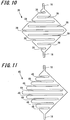
- FIG. 10 is a plan view showing a detection electrode 35 of a position detecting device according to another embodiment of the present invention.
- directions of open ends of slits 39 are alternately reversed as going from one vertex to the other vertex (to which the connecting portions 18 are connected).
- FIG. 11 is a plan view showing a detection electrode 45 of a position detecting device according to yet another embodiment of the present invention.
- each of the slits 49 extends from one side to the other side with respect to a line connecting two vertexes (to which the connecting portions 18 are connected), and is open at the outer edge of the one side and closed at the other side.
- the present invention is not limited to the embodiments described above and illustrated in the attached drawings. Various modifications can be made without departing from the scope of the present invention described in the claims.
- the housing and the input section are each formed in a quadrangular shape in the aforesaid embodiments, obviously the housing and the input section may also be formed in other shapes such as a circular shape, a triangular shape, a hexagonal shape, an octagon shape and the like.
- the slits are formed in a straight line shape with respect to the detection electrode in the aforesaid embodiments, the slits may also be formed in a corrugated (serpentine) or curved shape.
Claims (13)
- Section de détection de capacité électrostatique comprenant :une surface ;une pluralité d'électrodes de détection (15, 35, 45), moyennant quoi au moins l'une de ladite pluralité d'électrodes de détection (15, 35, 45) est prévue sur la surface, et possède une surface adaptée pour détecter une capacitance entre elle-même et une partie d'un corps humain ;dans laquelle la au moins une de ladite pluralité d'électrodes de détection (15, 35, 45) est munie d'au moins une fente (19, 39, 49) ;ladite section de détection de capacité électrostatique comprenant en outreun premier groupe d'électrodes de détection (16A) composé d'une pluralité d'électrodes de détection (15, 35, 45) prévues dans une première direction, et un second groupe d'électrodes de détection (16B) composé d'une pluralité d'électrodes de détection (15, 35, 45) prévues dans une seconde direction, la seconde direction étant différente de la première direction,dans laquelle les électrodes de détection (15, 35, 45) du premier groupe d'électrodes de détection (16A) sont munies d'une pluralité de premières fentes et les électrodes de détection (15, 35, 45) du second groupe d'électrodes de détection (16B) sont munies de secondes fentes,caractérisée en ce queles premières fentes s'étendent dans une direction différente de la direction dans laquelle les secondes fentes s'étendent.
- Section de détection de capacité électrostatique selon la revendication 1, dans laquelle les électrodes de détection (15, 35, 45) du premier groupe d'électrodes de détection (16A) sont disposées de manière linéaire dans une première direction, et les électrodes de détection (15, 35, 45) du second groupe d'électrodes de détection (16B) sont disposées de manière linéaire dans une seconde direction ;
dans laquelle les premières fentes s'étendent linéairement dans une direction différente de la direction dans laquelle les secondes fentes s'étendent. - Section de détection de capacité électrostatique selon la revendication 1, dans laquelle la au moins une fente (19, 39, 49) s'étend d'un bord externe de la au moins une électrode de détection (15, 35, 45) vers un bord interne de celle-ci, dans laquelle ladite fente (19, 39, 49) est ouverte au niveau du bord externe et fermée au niveau du bord interne de l'électrode de détection (15, 35, 45).
- Section de détection de capacité électrostatique selon la revendication 1, dans laquelle la au moins une fente (19, 39, 49) s'étend d'un bord de la au moins une électrode de détection (15, 35, 45) vers un autre bord de celle-ci.
- Section de détection de capacité électrostatique selon l'une des revendications 1 à 3, dans laquelle la au moins une électrode de détection de ladite pluralité d'électrodes de détection (15, 35, 45) est munie d'une pluralité de fentes (19, 39, 49) qui sont sensiblement parallèles les unes aux autres.
- Section de détection de capacité électrostatique selon l'une des revendications précédentes, comprenant en outre un circuit de mesure de capacitance (22) destiné à mesurer un changement de capacitance entre la au moins une électrode de détection (15, 35, 45) et la partie du corps humain.
- Dispositif de détection de position muni d'une section de détection de capacité électrostatique selon l'une des revendications précédentes, comprenant :une première section de détection sensiblement plate (13) ayant une surface et une autre surface ;la au moins une de la pluralité d'électrodes de détection (15, 35, 45) prévues sur la surface de la première section de détection (13), la au moins une de la pluralité d'électrodes de détection (15, 35, 45) étant configurée pour détecter une capacitance entre elle-même et une partie d'un corps humain ; et une seconde section de détection (14) prévue de façon à faire face à l'autre surface opposée à la surface de la première section de détection (13) et munie d'au moins une bobine hélicoïdale (24), dans lequel la au moins une de la pluralité d'électrodes de détection (15, 35, 45) est formée comme une électrode sensiblement plate et est munie d'au moins une fente (19, 39, 49).
- Dispositif de détection de position selon la revendication 7, dans lequel la première section de détection (13) comprend le premier groupe d'électrodes de détection (16A) dans lequel plusieurs électrodes de détection (15, 35, 45) sont prévues de manière linéaire dans une première direction sensiblement sur le même plan, et un second groupe d'électrodes de détection (16B) dans lequel plusieurs électrodes de détection (15, 35, 45) sont prévues de manière linéaire dans une seconde direction sur le même plan que celui du premier groupe d'électrodes de détection (16A), la seconde direction étant perpendiculaire à la première direction ;
dans lequel les électrodes de détection (15, 35, 45) du premier groupe d'électrodes de détection (16A) sont munies de plusieurs fentes (19, 39, 49) qui s'étendent linéairement dans la seconde direction et les électrodes de détection (15, 35, 45) du second groupe d'électrodes de détection (16B) sont munies de plusieurs fentes (19, 39, 49) qui s'étendent linéairement dans la première direction. - Dispositif de détection de position selon la revendication 7 ou 8, dans lequel la au moins une électrode de détection est de forme quadrangulaire.
- Dispositif de détection de position selon l'une des revendications 7 à 9, dans lequel la fente (19, 39, 49) est droite.
- Dispositif de détection de position selon l'une des revendications 7 à 9, dans lequel la fente (19, 39, 49) serpente.
- Dispositif de détection de position selon l'une des revendications 7 à 11, comprenant en outre :un indicateur de position (2) ayant au moins une bobine (27) et adapté pour générer un flux magnétique à partir de la bobine (27) ;dans lequel ladite au moins une bobine hélicoïdale (24) est adaptée pour détecter le flux magnétique,et dans lequel la au moins une de la pluralité d'électrodes de détection (15, 35, 45) est munie d'au moins une fente (19, 39, 49) qui s'étend d'un bord externe de celle-ci vers un bord interne de celle-ci, dans lequel ladite fente (19, 39, 49) est ouverte au niveau du bord externe et fermée au niveau du bord interne de l'électrode de détection (15, 35, 45).
- Dispositif de détection de position selon la revendication 9, dans lequel la première section de détection possède un circuit de mesure de capacitance (22) destiné à mesurer un changement de capacitance entre la au moins une de la pluralité d'électrodes de détection (15, 35, 45) et la partie du corps humain, et la seconde section de détection (14) possède un circuit de détection d'induction électromagnétique (23) destiné à détecter une position indiquée par l'indicateur de position (2).
Applications Claiming Priority (1)
| Application Number | Priority Date | Filing Date | Title |
|---|---|---|---|
| JP2007340099A JP5094376B2 (ja) | 2007-12-28 | 2007-12-28 | 位置検出装置 |
Publications (2)
| Publication Number | Publication Date |
|---|---|
| EP2077489A1 EP2077489A1 (fr) | 2009-07-08 |
| EP2077489B1 true EP2077489B1 (fr) | 2018-10-24 |
Family
ID=40427113
Family Applications (1)
| Application Number | Title | Priority Date | Filing Date |
|---|---|---|---|
| EP08022437.1A Active EP2077489B1 (fr) | 2007-12-28 | 2008-12-23 | Dispositif de détection de position |
Country Status (7)
| Country | Link |
|---|---|
| US (1) | US8228312B2 (fr) |
| EP (1) | EP2077489B1 (fr) |
| JP (1) | JP5094376B2 (fr) |
| KR (1) | KR101147020B1 (fr) |
| CN (1) | CN101470562B (fr) |
| IL (1) | IL196180A (fr) |
| TW (1) | TWI423085B (fr) |
Families Citing this family (100)
| Publication number | Priority date | Publication date | Assignee | Title |
|---|---|---|---|---|
| US8633915B2 (en) | 2007-10-04 | 2014-01-21 | Apple Inc. | Single-layer touch-sensitive display |
| US20090174676A1 (en) | 2008-01-04 | 2009-07-09 | Apple Inc. | Motion component dominance factors for motion locking of touch sensor data |
| TWI361996B (en) * | 2008-03-21 | 2012-04-11 | Elan Microelectronics Corp | Touch panel device |
| US8576193B2 (en) | 2008-04-25 | 2013-11-05 | Apple Inc. | Brick layout and stackup for a touch screen |
| US8487898B2 (en) | 2008-04-25 | 2013-07-16 | Apple Inc. | Ground guard for capacitive sensing |
| US8319747B2 (en) | 2008-12-11 | 2012-11-27 | Apple Inc. | Single layer touch panel with segmented drive and sense electrodes |
| BRPI0924132A2 (pt) | 2009-01-23 | 2016-02-10 | Qualcomm Mems Technologies Inc | dispositivo e sistema de iluminação e métodos de fabricação de dispositivo de iluminação e de detecção do movimento de objeto através de painel de iluminação |
| US9261997B2 (en) | 2009-02-02 | 2016-02-16 | Apple Inc. | Touch regions in diamond configuration |
| US8922521B2 (en) | 2009-02-02 | 2014-12-30 | Apple Inc. | Switching circuitry for touch sensitive display |
| WO2010117882A2 (fr) * | 2009-04-10 | 2010-10-14 | Apple Inc. | Conception d'écran à capteur tactile amélioré |
| US8593410B2 (en) | 2009-04-10 | 2013-11-26 | Apple Inc. | Touch sensor panel design |
| TWM366123U (en) * | 2009-04-10 | 2009-10-01 | Prime View Int Co Ltd | Touch control display apparatus and position indicator thereof |
| JP5366051B2 (ja) | 2009-04-20 | 2013-12-11 | 株式会社ジャパンディスプレイ | 情報入力装置、表示装置 |
| US8957874B2 (en) | 2009-06-29 | 2015-02-17 | Apple Inc. | Touch sensor panel design |
| JP5886489B2 (ja) | 2009-09-21 | 2016-03-16 | 株式会社ワコム | 位置検出装置 |
| JP5466908B2 (ja) | 2009-09-21 | 2014-04-09 | 株式会社ワコム | センサ基板および位置検出装置 |
| JP5430339B2 (ja) * | 2009-10-19 | 2014-02-26 | 株式会社ワコム | 位置検出装置及び位置指示器 |
| US9916045B2 (en) | 2009-10-26 | 2018-03-13 | Amtel Corporation | Sense electrode design |
| KR101027672B1 (ko) * | 2009-11-24 | 2011-04-12 | 유영기 | 손가락과 공진회로를 구비한 포인터의 위치를 동시에 검출할 수 있는 타블렛 |
| KR20110076188A (ko) * | 2009-12-29 | 2011-07-06 | 삼성전자주식회사 | 정전 용량 센싱 장치 및 제조방법 |
| JP5484097B2 (ja) * | 2010-01-27 | 2014-05-07 | 株式会社ワコム | 位置検出装置および方法 |
| JP5427070B2 (ja) * | 2010-03-05 | 2014-02-26 | 株式会社ワコム | 位置検出装置 |
| KR101113450B1 (ko) * | 2010-03-12 | 2012-02-29 | 삼성모바일디스플레이주식회사 | 터치 스크린 패널 |
| CN102200868B (zh) * | 2010-03-25 | 2013-02-13 | 太瀚科技股份有限公司 | 兼具电容感应与电磁感应功能的天线回路架构 |
| KR101093351B1 (ko) * | 2010-04-12 | 2011-12-14 | 삼성모바일디스플레이주식회사 | 터치 스크린 패널 |
| WO2012014206A2 (fr) * | 2010-07-28 | 2012-02-02 | N-Trig Ltd. | Capteur tactile capacitif de numériseur |
| US9652088B2 (en) | 2010-07-30 | 2017-05-16 | Apple Inc. | Fabrication of touch sensor panel using laser ablation |
| KR20120017587A (ko) * | 2010-08-19 | 2012-02-29 | 삼성모바일디스플레이주식회사 | 터치스크린패널 일체형 액정표시장치 |
| JP5611721B2 (ja) | 2010-08-20 | 2014-10-22 | 株式会社ワコム | 指示体検出装置、位置検出センサおよび位置検出センサの製造方法 |
| JP5685411B2 (ja) * | 2010-10-01 | 2015-03-18 | 京セラディスプレイ株式会社 | タッチパネル |
| CN102467270A (zh) * | 2010-11-02 | 2012-05-23 | 南京中铼光电有限公司 | 触控面板及触控感应垫 |
| JP5730551B2 (ja) | 2010-12-01 | 2015-06-10 | 株式会社ワコム | 指示体による指示位置を検出するための検出センサ、指示体位置検出装置および検出センサの製造方法 |
| TWI443569B (zh) * | 2011-02-23 | 2014-07-01 | Wintek Corp | 電容式觸控面板 |
| CN102681735A (zh) * | 2011-03-15 | 2012-09-19 | 东莞万士达液晶显示器有限公司 | 电容式触控面板 |
| CN102129324B (zh) * | 2011-03-17 | 2012-05-02 | 汉王科技股份有限公司 | 触控装置及其控制方法和具有该触控装置的电子设备 |
| TWI441053B (zh) * | 2011-03-24 | 2014-06-11 | Hannstar Display Corp | 觸控顯示裝置 |
| KR101711668B1 (ko) * | 2011-06-03 | 2017-03-13 | 삼성전자주식회사 | 채널을 공유하는 전자기 공진 센싱 장치 |
| JP5777094B2 (ja) * | 2011-07-14 | 2015-09-09 | 株式会社ワコム | 位置検出センサおよび位置検出装置 |
| TWM447538U (zh) | 2011-07-26 | 2013-02-21 | Byd Co Ltd | 感應單元、觸摸螢幕檢測裝置及觸控裝置 |
| CN102902433B (zh) * | 2011-07-26 | 2017-01-25 | 比亚迪股份有限公司 | 触摸检测方法及触控装置 |
| JP5871307B2 (ja) * | 2011-09-30 | 2016-03-01 | 株式会社ワコム | 位置検出センサユニットおよび位置検出装置 |
| JP5848589B2 (ja) * | 2011-12-02 | 2016-01-27 | 株式会社ワコム | 位置検出装置および位置検出方法 |
| US8599169B2 (en) * | 2011-12-14 | 2013-12-03 | Freescale Semiconductor, Inc. | Touch sense interface circuit |
| CN103186270B (zh) * | 2011-12-27 | 2016-08-10 | 宸鸿光电科技股份有限公司 | 感测电极结构及使用该感测电极结构的触控面板 |
| TWI467453B (zh) * | 2012-01-18 | 2015-01-01 | Chunghwa Picture Tubes Ltd | 雙模式觸控感應裝置 |
| CN103257757A (zh) * | 2012-02-17 | 2013-08-21 | 林志忠 | 触控面板的制造方法 |
| CN103257759A (zh) * | 2012-02-17 | 2013-08-21 | 林志忠 | 触控面板结构 |
| US9329723B2 (en) | 2012-04-16 | 2016-05-03 | Apple Inc. | Reconstruction of original touch image from differential touch image |
| US9600125B2 (en) * | 2012-07-18 | 2017-03-21 | Ctpress Semiconductor Corporation | Sensor array with edge pattern |
| CN103577084A (zh) * | 2012-08-01 | 2014-02-12 | 深圳市经纬科技有限公司 | 多模式触控输入方法及系统 |
| JP6021174B2 (ja) | 2012-08-08 | 2016-11-09 | 株式会社ワコム | 位置検出装置およびその位置指示器 |
| US9154189B2 (en) | 2012-08-17 | 2015-10-06 | Qualcomm Incorporated | Wireless power system with capacitive proximity sensing |
| US9483168B2 (en) | 2012-08-22 | 2016-11-01 | Google Inc. | Correcting scrolling gesture |
| JP5971708B2 (ja) * | 2012-08-27 | 2016-08-17 | 株式会社ジャパンディスプレイ | タッチパネル内蔵型表示装置 |
| KR101913817B1 (ko) * | 2012-08-29 | 2018-10-31 | 삼성전자주식회사 | 터치스크린 입력 처리 방법 및 장치 |
| US9389737B2 (en) | 2012-09-14 | 2016-07-12 | Samsung Display Co., Ltd. | Display device and method of driving the same in two modes |
| US11314368B2 (en) | 2012-09-14 | 2022-04-26 | Samsung Display Co., Ltd. | Display device and method of driving the same in two modes |
| TWI467458B (zh) * | 2012-09-21 | 2015-01-01 | Touchplus Information Corp | 電容式觸控裝置 |
| TWI483165B (zh) * | 2012-09-21 | 2015-05-01 | Au Optronics Corp | 電容式觸控感測結構及其應用 |
| US9007191B2 (en) | 2012-10-04 | 2015-04-14 | Google Inc. | Sensor pattern for a tactile input device |
| FR3005288B1 (fr) | 2013-05-06 | 2015-05-15 | Bic Soc | Dispositif manuel adapte pour un ecran capacitif |
| CN103278084A (zh) * | 2013-05-07 | 2013-09-04 | 苏州威仕科贸有限公司 | 一种汽车贴膜形状信息采集装置 |
| CN103273529A (zh) * | 2013-05-07 | 2013-09-04 | 苏州威仕科贸有限公司 | 一种汽车贴膜裁膜成套设备 |
| EP2830039B1 (fr) | 2013-07-24 | 2018-10-03 | Native Instruments GmbH | Procédé, dispositif, programme informatique et moyen de stockage lisible par ordinateur pour commander au moins un paramètre ou au moins un objet à l'aide d'éléments d'entrée de détection de capacité |
| US9886141B2 (en) | 2013-08-16 | 2018-02-06 | Apple Inc. | Mutual and self capacitance touch measurements in touch panel |
| KR20150027596A (ko) * | 2013-09-04 | 2015-03-12 | 삼성디스플레이 주식회사 | 전자기 공진 방식의 터치 센서 및 터치 센서를 포함하는 표시 장치 |
| KR102113685B1 (ko) * | 2013-10-08 | 2020-05-21 | 엘지디스플레이 주식회사 | 터치입력장치 |
| KR102087830B1 (ko) * | 2013-11-01 | 2020-04-14 | 엘지디스플레이 주식회사 | 터치 센싱 시스템과 그 구동 방법 |
| KR101617829B1 (ko) * | 2013-12-05 | 2016-05-03 | 주식회사 와이드벤티지 | 제한된 수의 자기장 센서를 이용한 사용자 입력 처리 장치 |
| JP6216252B2 (ja) * | 2014-01-09 | 2017-10-18 | アルプス電気株式会社 | 入力装置 |
| JP6327874B2 (ja) * | 2014-02-04 | 2018-05-23 | 株式会社ミツトヨ | 誘導型位置測定装置 |
| KR102193915B1 (ko) * | 2014-02-10 | 2020-12-23 | 삼성디스플레이 주식회사 | 터치 센서 기판 및 이를 포함하는 표시 장치 |
| KR101527321B1 (ko) * | 2014-02-26 | 2015-06-09 | 하이디스 테크놀로지 주식회사 | 터치 패널 |
| JP6327925B2 (ja) * | 2014-04-30 | 2018-05-23 | 株式会社ワコム | 位置検出装置 |
| WO2015178920A1 (fr) | 2014-05-22 | 2015-11-26 | Onamp Research Llc | Architectures d'amorçage de panneau pour capacité propre en cellule |
| KR101581672B1 (ko) * | 2014-06-09 | 2015-12-31 | 주식회사 더한 | 정전용량형 터치와 유도전자기장 입력을 동시에 감지하는 다중 입력 패드 및 입력 시스템 |
| US10289251B2 (en) | 2014-06-27 | 2019-05-14 | Apple Inc. | Reducing floating ground effects in pixelated self-capacitance touch screens |
| US9280251B2 (en) | 2014-07-11 | 2016-03-08 | Apple Inc. | Funneled touch sensor routing |
| US9880655B2 (en) | 2014-09-02 | 2018-01-30 | Apple Inc. | Method of disambiguating water from a finger touch on a touch sensor panel |
| CN107077260B (zh) | 2014-09-22 | 2020-05-12 | 苹果公司 | 触摸控制器和用于触摸传感器面板的方法 |
| KR102274944B1 (ko) | 2014-09-24 | 2021-07-08 | 삼성전자주식회사 | 오브젝트를 식별하는 전자 장치 및 방법 |
| CN104199588B (zh) * | 2014-09-24 | 2017-03-15 | 上海天马微电子有限公司 | 一种触摸屏及触控显示装置 |
| CN107077262B (zh) | 2014-10-27 | 2020-11-10 | 苹果公司 | 像素化自电容水排斥 |
| EP3224699B1 (fr) | 2015-02-02 | 2018-10-03 | Apple Inc. | Architecture flexible pour système de détection tactile à auto-capacité et capacités mutuelles |
| US10488992B2 (en) | 2015-03-10 | 2019-11-26 | Apple Inc. | Multi-chip touch architecture for scalability |
| TWI739723B (zh) * | 2015-05-21 | 2021-09-11 | 日商和冠股份有限公司 | 主動式觸控筆 |
| JP6487782B2 (ja) * | 2015-06-08 | 2019-03-20 | 株式会社ワコム | 位置指示器における構成タイプの設定方法 |
| US10534481B2 (en) | 2015-09-30 | 2020-01-14 | Apple Inc. | High aspect ratio capacitive sensor panel |
| US10365773B2 (en) | 2015-09-30 | 2019-07-30 | Apple Inc. | Flexible scan plan using coarse mutual capacitance and fully-guarded measurements |
| JP6639296B2 (ja) | 2016-03-23 | 2020-02-05 | 株式会社ジャパンディスプレイ | 表示装置 |
| AU2017208277B2 (en) | 2016-09-06 | 2018-12-20 | Apple Inc. | Back of cover touch sensors |
| CN109791459B (zh) * | 2016-10-06 | 2022-02-25 | 夏普株式会社 | 触摸面板和触摸面板系统 |
| JP6792506B2 (ja) * | 2017-04-18 | 2020-11-25 | 株式会社ジャパンディスプレイ | 表示装置 |
| US10642418B2 (en) | 2017-04-20 | 2020-05-05 | Apple Inc. | Finger tracking in wet environment |
| JP6334796B2 (ja) * | 2017-09-08 | 2018-05-30 | アルプス電気株式会社 | 入力装置 |
| JP6580190B2 (ja) * | 2018-04-16 | 2019-09-25 | 株式会社ワコム | 位置検出装置 |
| CN109030581B (zh) * | 2018-07-04 | 2024-04-16 | 南京铁道职业技术学院 | 一种复合结构的受电弓碳滑板表面损伤检测用电荷变换器 |
| KR102260916B1 (ko) | 2018-07-17 | 2021-06-04 | 주식회사 아하정보통신 | 동 메쉬를 이용한 정전용량방식 및 전자기유도 방식을 사용하는 터치 센서 |
| CN113168265A (zh) * | 2019-01-04 | 2021-07-23 | 株式会社和冠 | 位置检测装置及位置检测方法 |
| US11662867B1 (en) | 2020-05-30 | 2023-05-30 | Apple Inc. | Hover detection on a touch sensor panel |
Citations (1)
| Publication number | Priority date | Publication date | Assignee | Title |
|---|---|---|---|---|
| US20040239650A1 (en) * | 2003-06-02 | 2004-12-02 | Mackey Bob Lee | Sensor patterns for a capacitive sensing apparatus |
Family Cites Families (25)
| Publication number | Priority date | Publication date | Assignee | Title |
|---|---|---|---|---|
| JPS6224928Y2 (fr) * | 1980-11-25 | 1987-06-25 | ||
| US4733222A (en) | 1983-12-27 | 1988-03-22 | Integrated Touch Arrays, Inc. | Capacitance-variation-sensitive touch sensing array system |
| JPS60189530A (ja) * | 1984-03-09 | 1985-09-27 | Sharp Corp | 多目的入力装置 |
| JP2600347B2 (ja) * | 1988-11-19 | 1997-04-16 | 富士ゼロックス株式会社 | 入力表示一体型装置 |
| JPH02162410A (ja) * | 1988-12-15 | 1990-06-22 | Wacom Co Ltd | 座標入力装置及びその入力用指示器 |
| JPH03229494A (ja) * | 1990-02-05 | 1991-10-11 | Wacom Co Ltd | 磁気シールド板および該シールド板によってシールドされた電気機器、および磁気シールド方法 |
| JPH04127315A (ja) * | 1990-09-19 | 1992-04-28 | Fujitsu Ltd | パーソナル・コンピュータ |
| US5463388A (en) * | 1993-01-29 | 1995-10-31 | At&T Ipm Corp. | Computer mouse or keyboard input device utilizing capacitive sensors |
| JP3225716B2 (ja) * | 1993-10-28 | 2001-11-05 | ぺんてる株式会社 | 情報入力装置 |
| JPH07249352A (ja) * | 1994-03-08 | 1995-09-26 | Toshiba Corp | 真空遮断器 |
| JPH07302153A (ja) * | 1994-05-09 | 1995-11-14 | Wacom Co Ltd | 座標検出装置 |
| JPH096518A (ja) | 1995-06-16 | 1997-01-10 | Wacom Co Ltd | サイドスイッチ機構及びスタイラスペン |
| US5952998A (en) * | 1997-01-15 | 1999-09-14 | Compaq Computer Corporation | Transparent touchpad with flat panel display for personal computers |
| JP3758865B2 (ja) * | 1998-12-01 | 2006-03-22 | 富士ゼロックス株式会社 | 座標入力装置 |
| JP3351377B2 (ja) * | 1999-03-12 | 2002-11-25 | 日本電気株式会社 | 高周波回路装置 |
| US6297811B1 (en) * | 1999-06-02 | 2001-10-02 | Elo Touchsystems, Inc. | Projective capacitive touchscreen |
| JP2003223275A (ja) * | 2001-11-22 | 2003-08-08 | Omron Corp | 入力装置 |
| JP2005030901A (ja) * | 2003-07-11 | 2005-02-03 | Alps Electric Co Ltd | 容量センサ |
| JP4713946B2 (ja) | 2005-05-30 | 2011-06-29 | シャープ株式会社 | 液晶表示装置 |
| JP4750629B2 (ja) * | 2005-11-11 | 2011-08-17 | 株式会社ワコム | 位置検出装置及び位置検出用センス部品 |
| JP4648860B2 (ja) * | 2006-03-16 | 2011-03-09 | 株式会社ワコム | 位置検出装置及びコンピュータ |
| JP4787087B2 (ja) * | 2006-03-23 | 2011-10-05 | 株式会社ワコム | 位置検出装置及び情報処理装置 |
| WO2007129085A2 (fr) * | 2006-05-09 | 2007-11-15 | Sensopad Limited | Arrangement de navigation pour dispositif électronique |
| GB2439614B (en) | 2006-05-31 | 2008-12-24 | Harald Philipp | Two-dimensional position sensor |
| JP4972782B2 (ja) * | 2007-06-22 | 2012-07-11 | 株式会社ワコム | 位置検出装置 |
-
2007
- 2007-12-28 JP JP2007340099A patent/JP5094376B2/ja active Active
-
2008
- 2008-12-10 TW TW097148025A patent/TWI423085B/zh active
- 2008-12-17 KR KR1020080128525A patent/KR101147020B1/ko active IP Right Grant
- 2008-12-23 EP EP08022437.1A patent/EP2077489B1/fr active Active
- 2008-12-25 IL IL196180A patent/IL196180A/en active IP Right Grant
- 2008-12-29 CN CN2008101895189A patent/CN101470562B/zh active Active
- 2008-12-29 US US12/345,582 patent/US8228312B2/en active Active
Patent Citations (1)
| Publication number | Priority date | Publication date | Assignee | Title |
|---|---|---|---|---|
| US20040239650A1 (en) * | 2003-06-02 | 2004-12-02 | Mackey Bob Lee | Sensor patterns for a capacitive sensing apparatus |
Also Published As
| Publication number | Publication date |
|---|---|
| EP2077489A1 (fr) | 2009-07-08 |
| KR101147020B1 (ko) | 2012-05-17 |
| TWI423085B (zh) | 2014-01-11 |
| JP5094376B2 (ja) | 2012-12-12 |
| CN101470562A (zh) | 2009-07-01 |
| CN101470562B (zh) | 2012-11-28 |
| IL196180A (en) | 2013-08-29 |
| TW200928926A (en) | 2009-07-01 |
| KR20090072966A (ko) | 2009-07-02 |
| US20090166100A1 (en) | 2009-07-02 |
| US8228312B2 (en) | 2012-07-24 |
| IL196180A0 (en) | 2009-09-22 |
| JP2009162538A (ja) | 2009-07-23 |
Similar Documents
| Publication | Publication Date | Title |
|---|---|---|
| EP2077489B1 (fr) | Dispositif de détection de position | |
| US7911454B2 (en) | Information processing apparatus, position detecting apparatus and sensing part for performing a detection operation | |
| US8686969B2 (en) | Input apparatus with integrated detection sections of electromagnetic type and capacitive type | |
| EP3018565B1 (fr) | Téléphone intelligent | |
| KR101474594B1 (ko) | 위치 검출 장치 | |
| JP4714144B2 (ja) | 接触技術の改良 | |
| EP2333648B1 (fr) | Dispositif de détection de position | |
| KR20180023789A (ko) | 터치 입력 장치 | |
| US20120306802A1 (en) | Differential capacitance touch sensor | |
| CN106462263A (zh) | 位置指示器、位置检测装置以及位置检测装置的输入控制方法 | |
| WO2001027868A1 (fr) | Capteur tactile transparent flexible pour dispositifs electroniques | |
| EP2160673A1 (fr) | Améliorations pour des interfaces utilisateur ou en rapport avec celles-ci et dispositif et procédé associés | |
| JP4750629B2 (ja) | 位置検出装置及び位置検出用センス部品 | |
| CN110770686A (zh) | 用于检测笔发送出的笔信号的传感器 | |
| WO2011058562A1 (fr) | Capteur capacitif pour système de numériseur | |
| EP2461240B1 (fr) | Capteur de détection, dispositif de détection de position d'indicateur et procédé de fabrication du capteur de détection | |
| US20230325031A1 (en) | Touch input device | |
| EP2128743A1 (fr) | Appareil à écran tactile | |
| JP2013218647A (ja) | 静電容量式タッチパネルの導電模様構造、およびその構成方法 | |
| JP7232481B2 (ja) | タッチセンサパネル及びタッチ入力装置 | |
| KR102336301B1 (ko) | 터치센서패널 및 터치입력장치 | |
| JP7267916B2 (ja) | 位置検出センサ、位置検出装置および情報処理システム | |
| KR102005856B1 (ko) | 터치 입력 장치 | |
| JP5303674B2 (ja) | 位置検出装置及び静電容量方式検出部 | |
| KR102526461B1 (ko) | 터치 센서 및 이를 포함하는 터치 입력 장치 |
Legal Events
| Date | Code | Title | Description |
|---|---|---|---|
| PUAI | Public reference made under article 153(3) epc to a published international application that has entered the european phase |
Free format text: ORIGINAL CODE: 0009012 |
|
| AK | Designated contracting states |
Kind code of ref document: A1 Designated state(s): AT BE BG CH CY CZ DE DK EE ES FI FR GB GR HR HU IE IS IT LI LT LU LV MC MT NL NO PL PT RO SE SI SK TR |
|
| AX | Request for extension of the european patent |
Extension state: AL BA MK RS |
|
| 17P | Request for examination filed |
Effective date: 20100107 |
|
| AKX | Designation fees paid |
Designated state(s): DE GB |
|
| RAP1 | Party data changed (applicant data changed or rights of an application transferred) |
Owner name: WACOM CO., LTD. |
|
| 17Q | First examination report despatched |
Effective date: 20130703 |
|
| GRAP | Despatch of communication of intention to grant a patent |
Free format text: ORIGINAL CODE: EPIDOSNIGR1 |
|
| RIC1 | Information provided on ipc code assigned before grant |
Ipc: G06F 3/044 20060101AFI20180423BHEP Ipc: G06F 3/046 20060101ALI20180423BHEP Ipc: G06F 3/0354 20130101ALI20180423BHEP |
|
| INTG | Intention to grant announced |
Effective date: 20180516 |
|
| GRAS | Grant fee paid |
Free format text: ORIGINAL CODE: EPIDOSNIGR3 |
|
| GRAA | (expected) grant |
Free format text: ORIGINAL CODE: 0009210 |
|
| AK | Designated contracting states |
Kind code of ref document: B1 Designated state(s): DE GB |
|
| REG | Reference to a national code |
Ref country code: GB Ref legal event code: FG4D |
|
| REG | Reference to a national code |
Ref country code: DE Ref legal event code: R096 Ref document number: 602008057527 Country of ref document: DE |
|
| REG | Reference to a national code |
Ref country code: DE Ref legal event code: R097 Ref document number: 602008057527 Country of ref document: DE |
|
| PLBE | No opposition filed within time limit |
Free format text: ORIGINAL CODE: 0009261 |
|
| STAA | Information on the status of an ep patent application or granted ep patent |
Free format text: STATUS: NO OPPOSITION FILED WITHIN TIME LIMIT |
|
| 26N | No opposition filed |
Effective date: 20190725 |
|
| PGFP | Annual fee paid to national office [announced via postgrant information from national office to epo] |
Ref country code: GB Payment date: 20221223 Year of fee payment: 15 Ref country code: DE Payment date: 20220620 Year of fee payment: 15 |
|
| P01 | Opt-out of the competence of the unified patent court (upc) registered |
Effective date: 20230907 |