EP2023699B1 - Heat radiation package with semiconductor device - Google Patents
Heat radiation package with semiconductor device Download PDFInfo
- Publication number
- EP2023699B1 EP2023699B1 EP08161925.6A EP08161925A EP2023699B1 EP 2023699 B1 EP2023699 B1 EP 2023699B1 EP 08161925 A EP08161925 A EP 08161925A EP 2023699 B1 EP2023699 B1 EP 2023699B1
- Authority
- EP
- European Patent Office
- Prior art keywords
- substrate
- embedded wiring
- heat
- portions
- light emitting
- Prior art date
- Legal status (The legal status is an assumption and is not a legal conclusion. Google has not performed a legal analysis and makes no representation as to the accuracy of the status listed.)
- Ceased
Links
Images


Classifications
-
- H—ELECTRICITY
- H05—ELECTRIC TECHNIQUES NOT OTHERWISE PROVIDED FOR
- H05K—PRINTED CIRCUITS; CASINGS OR CONSTRUCTIONAL DETAILS OF ELECTRIC APPARATUS; MANUFACTURE OF ASSEMBLAGES OF ELECTRICAL COMPONENTS
- H05K3/00—Apparatus or processes for manufacturing printed circuits
- H05K3/10—Apparatus or processes for manufacturing printed circuits in which conductive material is applied to the insulating support in such a manner as to form the desired conductive pattern
- H05K3/107—Apparatus or processes for manufacturing printed circuits in which conductive material is applied to the insulating support in such a manner as to form the desired conductive pattern by filling grooves in the support with conductive material
-
- H—ELECTRICITY
- H01—ELECTRIC ELEMENTS
- H01L—SEMICONDUCTOR DEVICES NOT COVERED BY CLASS H10
- H01L23/00—Details of semiconductor or other solid state devices
- H01L23/48—Arrangements for conducting electric current to or from the solid state body in operation, e.g. leads, terminal arrangements ; Selection of materials therefor
- H01L23/488—Arrangements for conducting electric current to or from the solid state body in operation, e.g. leads, terminal arrangements ; Selection of materials therefor consisting of soldered or bonded constructions
- H01L23/498—Leads, i.e. metallisations or lead-frames on insulating substrates, e.g. chip carriers
- H01L23/49861—Lead-frames fixed on or encapsulated in insulating substrates
-
- H—ELECTRICITY
- H05—ELECTRIC TECHNIQUES NOT OTHERWISE PROVIDED FOR
- H05K—PRINTED CIRCUITS; CASINGS OR CONSTRUCTIONAL DETAILS OF ELECTRIC APPARATUS; MANUFACTURE OF ASSEMBLAGES OF ELECTRICAL COMPONENTS
- H05K1/00—Printed circuits
- H05K1/02—Details
- H05K1/0201—Thermal arrangements, e.g. for cooling, heating or preventing overheating
- H05K1/0203—Cooling of mounted components
-
- H—ELECTRICITY
- H10—SEMICONDUCTOR DEVICES; ELECTRIC SOLID-STATE DEVICES NOT OTHERWISE PROVIDED FOR
- H10H—INORGANIC LIGHT-EMITTING SEMICONDUCTOR DEVICES HAVING POTENTIAL BARRIERS
- H10H20/00—Individual inorganic light-emitting semiconductor devices having potential barriers, e.g. light-emitting diodes [LED]
- H10H20/80—Constructional details
- H10H20/85—Packages
- H10H20/8506—Containers
-
- H—ELECTRICITY
- H01—ELECTRIC ELEMENTS
- H01L—SEMICONDUCTOR DEVICES NOT COVERED BY CLASS H10
- H01L2224/00—Indexing scheme for arrangements for connecting or disconnecting semiconductor or solid-state bodies and methods related thereto as covered by H01L24/00
- H01L2224/01—Means for bonding being attached to, or being formed on, the surface to be connected, e.g. chip-to-package, die-attach, "first-level" interconnects; Manufacturing methods related thereto
- H01L2224/10—Bump connectors; Manufacturing methods related thereto
- H01L2224/15—Structure, shape, material or disposition of the bump connectors after the connecting process
- H01L2224/16—Structure, shape, material or disposition of the bump connectors after the connecting process of an individual bump connector
-
- H—ELECTRICITY
- H01—ELECTRIC ELEMENTS
- H01L—SEMICONDUCTOR DEVICES NOT COVERED BY CLASS H10
- H01L23/00—Details of semiconductor or other solid state devices
- H01L23/34—Arrangements for cooling, heating, ventilating or temperature compensation ; Temperature sensing arrangements
- H01L23/36—Selection of materials, or shaping, to facilitate cooling or heating, e.g. heatsinks
- H01L23/373—Cooling facilitated by selection of materials for the device or materials for thermal expansion adaptation, e.g. carbon
- H01L23/3735—Laminates or multilayers, e.g. direct bond copper ceramic substrates
-
- H—ELECTRICITY
- H05—ELECTRIC TECHNIQUES NOT OTHERWISE PROVIDED FOR
- H05K—PRINTED CIRCUITS; CASINGS OR CONSTRUCTIONAL DETAILS OF ELECTRIC APPARATUS; MANUFACTURE OF ASSEMBLAGES OF ELECTRICAL COMPONENTS
- H05K1/00—Printed circuits
- H05K1/02—Details
- H05K1/0213—Electrical arrangements not otherwise provided for
- H05K1/0263—High current adaptations, e.g. printed high current conductors or using auxiliary non-printed means; Fine and coarse circuit patterns on one circuit board
-
- H—ELECTRICITY
- H05—ELECTRIC TECHNIQUES NOT OTHERWISE PROVIDED FOR
- H05K—PRINTED CIRCUITS; CASINGS OR CONSTRUCTIONAL DETAILS OF ELECTRIC APPARATUS; MANUFACTURE OF ASSEMBLAGES OF ELECTRICAL COMPONENTS
- H05K1/00—Printed circuits
- H05K1/02—Details
- H05K1/03—Use of materials for the substrate
- H05K1/0306—Inorganic insulating substrates, e.g. ceramic, glass
-
- H—ELECTRICITY
- H05—ELECTRIC TECHNIQUES NOT OTHERWISE PROVIDED FOR
- H05K—PRINTED CIRCUITS; CASINGS OR CONSTRUCTIONAL DETAILS OF ELECTRIC APPARATUS; MANUFACTURE OF ASSEMBLAGES OF ELECTRICAL COMPONENTS
- H05K2201/00—Indexing scheme relating to printed circuits covered by H05K1/00
- H05K2201/10—Details of components or other objects attached to or integrated in a printed circuit board
- H05K2201/10007—Types of components
- H05K2201/10106—Light emitting diode [LED]
-
- H—ELECTRICITY
- H05—ELECTRIC TECHNIQUES NOT OTHERWISE PROVIDED FOR
- H05K—PRINTED CIRCUITS; CASINGS OR CONSTRUCTIONAL DETAILS OF ELECTRIC APPARATUS; MANUFACTURE OF ASSEMBLAGES OF ELECTRICAL COMPONENTS
- H05K3/00—Apparatus or processes for manufacturing printed circuits
- H05K3/0058—Laminating printed circuit boards onto other substrates, e.g. metallic substrates
- H05K3/0061—Laminating printed circuit boards onto other substrates, e.g. metallic substrates onto a metallic substrate, e.g. a heat sink
-
- H—ELECTRICITY
- H05—ELECTRIC TECHNIQUES NOT OTHERWISE PROVIDED FOR
- H05K—PRINTED CIRCUITS; CASINGS OR CONSTRUCTIONAL DETAILS OF ELECTRIC APPARATUS; MANUFACTURE OF ASSEMBLAGES OF ELECTRICAL COMPONENTS
- H05K3/00—Apparatus or processes for manufacturing printed circuits
- H05K3/10—Apparatus or processes for manufacturing printed circuits in which conductive material is applied to the insulating support in such a manner as to form the desired conductive pattern
- H05K3/108—Apparatus or processes for manufacturing printed circuits in which conductive material is applied to the insulating support in such a manner as to form the desired conductive pattern by semi-additive methods; masks therefor
-
- H—ELECTRICITY
- H10—SEMICONDUCTOR DEVICES; ELECTRIC SOLID-STATE DEVICES NOT OTHERWISE PROVIDED FOR
- H10H—INORGANIC LIGHT-EMITTING SEMICONDUCTOR DEVICES HAVING POTENTIAL BARRIERS
- H10H20/00—Individual inorganic light-emitting semiconductor devices having potential barriers, e.g. light-emitting diodes [LED]
- H10H20/80—Constructional details
- H10H20/85—Packages
- H10H20/857—Interconnections, e.g. lead-frames, bond wires or solder balls
-
- H—ELECTRICITY
- H10—SEMICONDUCTOR DEVICES; ELECTRIC SOLID-STATE DEVICES NOT OTHERWISE PROVIDED FOR
- H10H—INORGANIC LIGHT-EMITTING SEMICONDUCTOR DEVICES HAVING POTENTIAL BARRIERS
- H10H20/00—Individual inorganic light-emitting semiconductor devices having potential barriers, e.g. light-emitting diodes [LED]
- H10H20/80—Constructional details
- H10H20/85—Packages
- H10H20/858—Means for heat extraction or cooling
- H10H20/8581—Means for heat extraction or cooling characterised by their material
-
- H—ELECTRICITY
- H10—SEMICONDUCTOR DEVICES; ELECTRIC SOLID-STATE DEVICES NOT OTHERWISE PROVIDED FOR
- H10H—INORGANIC LIGHT-EMITTING SEMICONDUCTOR DEVICES HAVING POTENTIAL BARRIERS
- H10H20/00—Individual inorganic light-emitting semiconductor devices having potential barriers, e.g. light-emitting diodes [LED]
- H10H20/80—Constructional details
- H10H20/85—Packages
- H10H20/858—Means for heat extraction or cooling
- H10H20/8585—Means for heat extraction or cooling being an interconnection
Definitions
- the present invention relates to a heat radiation package and a semiconductor device and, more particularly, a heat radiation package in which a semiconductor element such as light emitting element, or the like, which generates a heat, is mounted and a semiconductor device using the same.
- Patent Literature 1 Patent Application Publication (KOKAI) 2005-116990 )
- LED element is mounted on a metal base portion, to which a metal reflecting mirror acting as a reflecting mirror/radiation body is joined, via a submount, thereby a heat from the LED element is guided to the metal base portion and the metal reflecting mirror and is radiated from there.
- Patent Literature 2 Patent Application Publication (KOKAI) 2004-207367 )
- a light emitting element is mounted on a circuit pattern, which is provided on a ceramic substrate, via gold bumps and also a radiating plate is provided under the ceramic substrate, thereby a heat from the light emitting element is radiated from the radiating plate to the outside via the gold bumps and the ceramic substrate.
- JP 11 068263 discloses a heat radiation package comprising: a resin substrate in an upper surface side of which a plurality of recess portions is provided; embedded wiring portions on which a semiconductor element which generates heat is to be mounted, which portions comprise a metal plating layer and are filled in respective ones of the recess portions; and a heat sink connected to a lower surface side of the substrate.
- a semiconductor device comprising: a substrate, made of silicon, in an upper surface side of which substrate a plurality of recess portions is provided; an insulating layer formed on the upper surface of the substrate including the recess portions; embedded wiring portions which are filled in the recess portions of the substrate respectively such that upper surfaces of the embedded wiring portions protrude to a predetermined height from the upper surface side of the substrate, the embedded wiring portions being formed of a seed layer and a copper plating layer formed on the seed layer; a semiconductor element electrically connected to the embedded wiring portion; and a heat sink connected to a lower surface side of the substrate; wherein a thickness of each embedded wiring' portion is set thicker than a thickness of the corresponding underlying portion of the substrate.
- the wiring substrate on which the semiconductor element (light emitting element, or the like) which generates a heat is mounted is constructed by filling the thick embedded wiring portion in the recess portion of the substrate.
- the embedded wiring portion is made of copper, a thermal conductivity of which is high (400 W/mK).
- the wiring substrate when viewed in the thickness direction of the wiring substrate, is constructed such that the upper main portion is formed of the embedded wiring portion whose thermal conductivity is high, and also the substrate remains under the embedded wiring portion as the supporting plate. Also, the substrate intervenes between the embedded wiring portions mutually.
- the embedded wiring portion is used not only as the wiring layer on which the semiconductor element is mounted, and functions but also as the heat diffusing portion for diffusing smoothly a heat into the heat sink. Therefore, a thermal conduction of the overall wiring substrate can be improved remarkably rather than the case where the wiring layer is formed over the whole plate-like insulating substrate.
- the semiconductor element which generates a heat can be cooled and held at a predetermined temperature, a malfunction or a thermal breakdown of the semiconductor element caused due to the heat can be prevented.
- an area of the embedded wiring portions are set larger (for example, about 2 times) than an area of the semiconductor elements which are to be mounted.
- FIG.1 is a sectional view showing a method of manufacturing a heat radiation package in the related art.
- a wiring layer 120 is provided on an insulating substrate 100.
- the insulating substrate 100 is formed of an insulating resin, alumina ceramics, or aluminum nitride ceramics.
- Bumps 220 of light emitting elements 200 (LED, or the like) are mounted to be connected to the wiring layer 120 provided on the insulating substrate 100.
- a heat sink 400 having a plurality of fins 420 is provided under the insulating substrate 100 via a heat conduction sheet 300.
- the heat sink 400 is formed of copper or aluminum.
- a heat generated from the light emitting elements 200 is transmitted to the heat sink 400 while using the insulating substrate 100 as the heat diffusion path and is emitted to the outside.
- thermal conductivities between the insulating substrate 100 of the heat radiation package 3 in the related art and the heat sink 400 are compared mutually.
- the insulating substrate 100 is formed of an insulating resin
- its thermal conductivity is 1 W/mK.
- the insulating substrate 100 is formed of alumina ceramics
- its thermal conductivity is several tens (10 to 30) W/mK.
- the insulating substrate 100 is formed of aluminum nitride ceramics
- its thermal conductivity is 170 W/mK.
- the heat sink 400 is formed of a copper, in view of the fact that its thermal conductivity is 400 W/mK, a thermal conduction of the insulating substrate 100 is considerably inferior as compared with the heat sink 400.
- a heat radiation package of the present embodiment explained hereunder can solve such problem.
- the heat radiation package of the present embodiment will be explained hereunder.
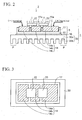
- FIG.2 is a sectional view showing a heat radiation package of an embodiment of the present invention.
- FIG.3 is a plan view of the heat radiation package in FIG.2 when viewed from the top.
- a plurality of recess portions C spot facing are provided in the upper surface side of a silicon substrate 10.
- An insulating layer 12 made of a silicon oxide layer is formed on an upper surface of the silicon substrate 10, containing inner surfaces of the recess portions C.
- An embedded wiring portion 14 made of a copper is filled in the recess portions C respectively.
- the embedded wiring portions 14 and the silicon substrate 10 are insulated electrically with the insulating layer 12.
- a wiring substrate 5 is constructed by the silicon substrate 10 and the embedded wiring portions 14.
- first, second, and third embedded wiring portions 14a, 14b, 14c are filled in three recess portions C provided on the silicon substrate 10 respectively. Also, upper surfaces of the embedded wiring portions 14 are protruded from an upper surface of the insulating layer 12 on the silicon substrate 10 like the example in FIG.2 .
- a thickness of the silicon substrate 10 is set to 200 to 700 ⁇ m, and a thickness of the embedded wiring portion 14 is set to 50 to 300 ⁇ m.
- a depth of the recess portion C in the silicon substrate 10 is decided in consideration of a thickness of the embedded wiring portion 14, and is set shallower than a thickness of the embedded wiring portion 14.
- the embedded wiring portions 14 and the silicon substrate 10 constitute the heat diffusion paths downwardly.
- a thermal conductivity of the embedded wiring portion 14 (which is copper) is 400 W/mK, and a thermal conductivity of the silicon substrate 10 is 140 W/mK that is lower than a thermal conductivity of the embedded wiring portion 14. Therefore, in order to diffuse smoothly a heat toward the lower side, a thickness of the embedded wiring portion 14 must be set thicker than a thickness of the underlying silicon substrate 10.
- a heat conduction sheet 16 whose thermal conduction is enhanced by dispersing silver (Ag) fillers, or the like is provided on the lower surface of the silicon substrate 10.
- a heat sink 30 (radiating portion) made of copper, aluminum, or the like is provided under the heat conduction sheet 16.
- the heat sink 30 is constructed by a base substance portion 30a and a plurality of fins 30b protruded from the base substance portion 30a downward.
- the heat sink 30 is provided to have a larger area than the silicon substrate 10.
- a protruded portion P that extends outward from the periphery of the silicon substrate 10 to the outside is provided.
- the heat sink 30 increases its surface area by using the fins 30b, thereby a cooling effect caused by airflow is enhance.
- the heat sink 30 may be fitted directly to the lower surface of the silicon substrate 10 via the heat conduction sheet 16 like the example in FIG.2 . Otherwise, a thin-film sheet-like heat pipe having a high thermal conductivity may be extended from the lower surface of the silicon substrate 10 to the outside, and then the heat sink 30 may be fitted to its end portion.
- the heat radiation package 1 of the present embodiment is constructed basically by the wiring substrate 5 composed of the silicon substrate 10 and the embedded wiring portions 14 filled in the recess portions C, the heat conduction sheet 16 provided under the silicon substrate 10, and the heat sink 30 provided under the heat conduction sheet 16.
- respective connecting connection terminals 20a, 22a such as gold bumps or the like, of a first light emitting element 20 and a second light emitting element 22 are mounted to be connected the embedded wiring portions 14 respectively.
- respective connection electrodes of the first and second light emitting elements 20, 22 may be connected to the connection terminals 20a, 22a provided on the embedded wiring portions 14.
- Each of the first and second light emitting elements 20, 22 has a plus (+) electrode and a minus (-) electrode.
- the plus (+) electrode of the first light emitting element 20 is connected to the first embedded wiring portion 14a to which a plus (+) terminal of an external circuit is connected, and the minus (-) electrode thereof is connected to the second embedded wiring portion 14b.
- the minus (-) electrode of the second light emitting element 22 is connected to the third embedded wiring portion 14c to which a minus (-) terminal of the external circuit is connected, and the plus (+) electrode thereof is connected to the second embedded wiring portion 14b.
- first light emitting element 20 and the second light emitting element 22 are connected electrically in series and are mounted. Also, the first and second light emitting element 20, 22 are mounted to direct their light emitting portions L to the upper side, as a consequence a light is emitted to the upper side.
- a semiconductor device 2 of the present embodiment is constructed by mounting the first and second light emitting elements 20, 22 on the embedded wiring portions 14 of the heat radiation package 1.
- the embedded wiring portions 14 whose thickness is thick and whose volume is large are formed to be filled in the recess portions C of the silicon substrate 10.
- the embedded wiring portions 14 are formed of a copper (400 W/mK) whose thermal conductivity is high, or the like.
- the wiring substrate 5 is constructed such that, when viewed in the thickness direction, the upper main portion is formed of the embedded wiring portions 14 whose thermal conductivity is high and also the silicon substrate 10 still remains under the embedded wiring portions 14 as the supporting plate. Also, because the recess portions C are provided in the silicon substrate 10, the silicon substrate 10 is interposed between the embedded wiring portions 14 mutually.
- the first to third embedded wiring portions 14a to 14c are provided like a quadrangular shape respectively, and a total area of them is set larger than a total area of the first and second light emitting elements 20, 22 (for example, two times to five times).
- the embedded wiring portions 14 are used not only as the wirings (electrodes) on which the light emitting elements 20, 22 are mounted but also as the heat diffusing portion that diffuses smoothly a heat into the heat sink 30.
- a thermal conductivity (140 W/mK) of the silicon substrate 10 is lower than a thermal conductivity (400 W/mK) of the embedded wiring portions 14 (copper), nevertheless the silicon substrate 10 having a lowest minimum thickness that allows to function as the supporting plate can be set to remain between the embedded wiring portions 14 and the heat sink 30 by providing the recess portions C. Therefore, a thermal conduction of the overall wiring substrate 5 (the silicon substrate 10 and the embedded wiring portions 14) can be improved remarkably rather than the case where the wiring layer 120 is formed on the overall plate-like insulating substrate 100 in the related art.
- the embedded wiring portions 14 are made of a copper whose thermal conductivity is high, or the like, whose thickness is thick, and whose area (volume) is large.
- a heat from the first and second light emitting elements 20, 22 diffuses smoothly into the embedded wiring portions 14.
- a heat transmitted through the embedded wiring portions 14 diffuses into the silicon substrate 10.
- the embedded wiring portions 14 acting as the heat diffusing portion whose thermal conduction is high are provided under the light emitting elements. Therefore, even when the light emitting elements such as LED whose heat radiation is high are mounted, the light emitting elements 20, 22 can be cooled sufficiently. As a result, a malfunction or a thermal breakdown caused by the heat generation can be prevented, and thus reliability can be improved.
- a semiconductor device 2a of a variation of the present embodiment is shown in FIG.4 .
- an insulating substrate 10a is used in place of the silicon substrate 10, and a plurality of recess portions C are provided in its upper surface side. Also, the similar embedded wiring portions 14 are filled in the recess portions C of the insulating substrate 10a.
- the material of the insulating substrate 10a aluminum nitride ceramics (thermal conductivity: 170 W/mK), alumina ceramics (thermal conductivity: several tens W/mK), or the like is employed.
- aluminum nitride ceramics having a high thermal conductivity should be employed as the insulating substrate 10a.
- the above insulating layer 12 in FIG.2 is omitted.
- Other elements are similar to those of the semiconductor device 2 in FIG.2 , and therefore their explanation will be omitted by affixing the same reference symbols to them.
- the semiconductor device 2a of the present variation can achieve the similar advantage to those of the semiconductor device 2 in FIG.2 .
- the light emitting elements are illustrated as the semiconductor element which generates a heat.
- the heat radiation package of the present embodiment can be used effectively as the heat radiation package for various semiconductor elements (LSI chip) generating the heat such as CPU device, and the like.
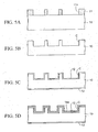
- the wafer-like silicon substrate 10 whose thickness is about 700 ⁇ m is prepared, and then a mask layer 11 such as a resist, or the like, in which opening portions 11x are provided, is formed on the silicon substrate 10.
- the opening portions 11x of the mask layer 11 are arranged to correspond to the recess portions C of the above silicon substrate 10.
- the dry etching is applied to the silicon substrate 10 through the opening portions 11x of the mask layer 11.
- the silicon substrate 10 is etched to halfway of its thickness.
- the mask layer 11 is removed.
- a plurality of recess portions C are formed in the silicon substrate 10.
- a silicon oxide layer is formed on an upper surface containing inner surfaces of the recess portions C and a lower surface of the silicon substrate 10 by thermally oxidizing the silicon substrate 10.
- the insulating layer 12 is obtained.
- a silicon oxide layer may be formed on the upper surface side or both surface sides of the silicon substrate 10 by the CVD method as the insulating layer 12.
- the seed layer 14a made of copper, or the like is formed on the upper surface side of the silicon substrate containing inner surfaces of the recess portions C by sputtering method.
- a plating resist 13 in which opening portions 13x are provided in portions that correspond to the recess portions C of the silicon substrate 10 is formed on the seed layer 14a.
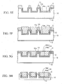
- the electroplating is applied to the silicon substrate 10 by utilizing the seed layer 14a as a plating power feeding path.
- the metal plating layer 14b made of copper, or the like is formed in the opening portions 13x of the plating resist 13.
- the metal plating layers 14b are formed to protrude from an upper surface of the plating resist 13.
- the metal plating layers 14b and the plating resist 13 are polished by CMP to planarize the upper surface side, and also a height of the metal plating layers 14b is adjusted at a predetermined height.
- the plating resist 13 is removed.
- the seed layer 14a is etched by using the metal plating layers 14b as a mask.
- the embedded wiring portions 14 each composed of the seed layer 14a and the metal plating layers 14b are obtained.
- the back surface side of the silicon substrate 10 is ground by the grinder such that a thickness of the silicon substrate 10 is adjusted to a predetermined thickness.
- the silicon substrate 10 is divided by the cutting to get individual wiring substrates 5.
- the heat sink 30 is mounted on the lower surface of the wiring substrate 5 via the heat conduction sheet 16.
- the fine patterning can be applied to the silicon substrate 10 by the wafer process (the photolithography and the dry etching, and the like), a miniaturization of the embedded wiring portions 14 can be implemented in contrast to the case where the ceramics or the insulating resin is used as the substrate. Therefore, not only the pad-like embedded wiring portions 14 as shown in Fig.2 can be formed, but also the embedded wiring portions 14 as the fine wirings can be drawn around with a narrow pitch. As a result, the package of the present embodiment can be used as the mounting substrate (heat radiation package) for the higher-performance semiconductor device.
Landscapes
- Engineering & Computer Science (AREA)
- Microelectronics & Electronic Packaging (AREA)
- Physics & Mathematics (AREA)
- Condensed Matter Physics & Semiconductors (AREA)
- General Physics & Mathematics (AREA)
- Computer Hardware Design (AREA)
- Power Engineering (AREA)
- Manufacturing & Machinery (AREA)
- Led Device Packages (AREA)
- Cooling Or The Like Of Semiconductors Or Solid State Devices (AREA)
Applications Claiming Priority (1)
| Application Number | Priority Date | Filing Date | Title |
|---|---|---|---|
| JP2007208883A JP5188120B2 (ja) | 2007-08-10 | 2007-08-10 | 半導体装置 |
Publications (3)
| Publication Number | Publication Date |
|---|---|
| EP2023699A2 EP2023699A2 (en) | 2009-02-11 |
| EP2023699A3 EP2023699A3 (en) | 2010-11-24 |
| EP2023699B1 true EP2023699B1 (en) | 2015-07-08 |
Family
ID=40010695
Family Applications (1)
| Application Number | Title | Priority Date | Filing Date |
|---|---|---|---|
| EP08161925.6A Ceased EP2023699B1 (en) | 2007-08-10 | 2008-08-06 | Heat radiation package with semiconductor device |
Country Status (4)
| Country | Link |
|---|---|
| US (1) | US8368206B2 (enExample) |
| EP (1) | EP2023699B1 (enExample) |
| JP (1) | JP5188120B2 (enExample) |
| TW (1) | TW200910539A (enExample) |
Families Citing this family (29)
| Publication number | Priority date | Publication date | Assignee | Title |
|---|---|---|---|---|
| US9172012B2 (en) | 2007-10-31 | 2015-10-27 | Cree, Inc. | Multi-chip light emitter packages and related methods |
| US9082921B2 (en) * | 2007-10-31 | 2015-07-14 | Cree, Inc. | Multi-die LED package |
| US9666762B2 (en) | 2007-10-31 | 2017-05-30 | Cree, Inc. | Multi-chip light emitter packages and related methods |
| KR20100094246A (ko) * | 2009-02-18 | 2010-08-26 | 엘지이노텍 주식회사 | 발광소자 패키지 및 그 제조방법 |
| KR100969146B1 (ko) | 2009-02-18 | 2010-07-08 | 엘지이노텍 주식회사 | 반도체 발광소자 및 그 제조방법 |
| KR101064098B1 (ko) | 2009-02-23 | 2011-09-08 | 엘지이노텍 주식회사 | 발광소자 패키지 및 그 제조방법 |
| JP5305987B2 (ja) * | 2009-03-02 | 2013-10-02 | キヤノン株式会社 | 放熱ユニット及び露光装置 |
| TWM366757U (en) * | 2009-04-27 | 2009-10-11 | Forward Electronics Co Ltd | AC LED packaging structure |
| US8749978B2 (en) * | 2010-01-29 | 2014-06-10 | Nitto Denko Corporation | Power module |
| CN201829527U (zh) * | 2010-05-31 | 2011-05-11 | 景德镇正宇奈米科技有限公司 | 具蜂巢状辐射散热装置的发光二极管结构 |
| US9159892B2 (en) * | 2010-07-01 | 2015-10-13 | Citizen Holdings Co., Ltd. | LED light source device and manufacturing method for the same |
| US10433414B2 (en) * | 2010-12-24 | 2019-10-01 | Rayben Technologies (HK) Limited | Manufacturing method of printing circuit board with micro-radiators |
| CN107425103B (zh) | 2011-08-22 | 2019-12-27 | Lg伊诺特有限公司 | 发光器件封装件和光装置 |
| KR101976531B1 (ko) * | 2011-12-22 | 2019-08-28 | 엘지이노텍 주식회사 | 발광 모듈 |
| KR101852390B1 (ko) * | 2011-11-18 | 2018-04-26 | 엘지이노텍 주식회사 | 광원 모듈 |
| JP2013153068A (ja) * | 2012-01-25 | 2013-08-08 | Shinko Electric Ind Co Ltd | 配線基板、発光装置及び配線基板の製造方法 |
| US9089075B2 (en) * | 2012-03-27 | 2015-07-21 | Gerald Ho Kim | Silicon-based cooling package for cooling and thermally decoupling devices in close proximity |
| KR101946912B1 (ko) * | 2012-05-14 | 2019-02-12 | 엘지이노텍 주식회사 | 광원모듈 및 이를 구비한 조명 시스템 |
| EP2919286A4 (en) | 2012-11-06 | 2016-05-11 | Ngk Insulators Ltd | SUBSTRATE FOR LIGHT-EMITTING DIODES |
| WO2014073039A1 (ja) | 2012-11-06 | 2014-05-15 | 日本碍子株式会社 | 発光ダイオード用基板 |
| DE102015205354A1 (de) * | 2015-03-24 | 2016-09-29 | Osram Gmbh | Optoelektronische Baugruppe und Verfahren zum Herstellen einer optoelektronischen Baugruppe |
| DE102015111307A1 (de) * | 2015-07-13 | 2017-01-19 | Epcos Ag | Bauelement mit verbesserter Wärmeableitung |
| JP2018120999A (ja) * | 2017-01-27 | 2018-08-02 | 日本特殊陶業株式会社 | 配線基板 |
| CN112753109B (zh) * | 2018-10-03 | 2024-04-05 | 西铁城电子株式会社 | 嵌体基板和使用该嵌体基板的发光装置 |
| JP7307874B2 (ja) * | 2019-04-26 | 2023-07-13 | 日亜化学工業株式会社 | 発光装置及び発光モジュール |
| JP7497578B2 (ja) * | 2020-02-26 | 2024-06-11 | 富士フイルムビジネスイノベーション株式会社 | 発光装置、光学装置及び情報処理装置 |
| DE102020112276A1 (de) * | 2020-05-06 | 2021-11-11 | Danfoss Silicon Power Gmbh | Leistungsmodul |
| US12021016B2 (en) * | 2020-06-10 | 2024-06-25 | Intel Corporation | Thermally enhanced silicon back end layers for improved thermal performance |
| JP7745427B2 (ja) * | 2021-10-26 | 2025-09-29 | デンカ株式会社 | 回路基板 |
Citations (2)
| Publication number | Priority date | Publication date | Assignee | Title |
|---|---|---|---|---|
| EP1261021A2 (en) * | 2001-05-21 | 2002-11-27 | Shinko Electric Industries Co. Ltd. | Method of production of circuit board, semiconductor device, and plating system |
| US20050035366A1 (en) * | 2003-08-13 | 2005-02-17 | Citizen Electronics Co., Ltd. | Light emitting diode |
Family Cites Families (21)
| Publication number | Priority date | Publication date | Assignee | Title |
|---|---|---|---|---|
| JP2914342B2 (ja) * | 1997-03-28 | 1999-06-28 | 日本電気株式会社 | 集積回路装置の冷却構造 |
| JP4114975B2 (ja) * | 1997-08-18 | 2008-07-09 | 松下電器産業株式会社 | 電子回路基板 |
| US6517218B2 (en) * | 2000-03-31 | 2003-02-11 | Relume Corporation | LED integrated heat sink |
| US6535396B1 (en) * | 2000-04-28 | 2003-03-18 | Delphi Technologies, Inc. | Combination circuit board and segmented conductive bus substrate |
| JP4742409B2 (ja) * | 2000-08-23 | 2011-08-10 | イビデン株式会社 | プリント配線板の製造方法 |
| TW521409B (en) * | 2000-10-06 | 2003-02-21 | Shing Chen | Package of LED |
| US7268479B2 (en) * | 2001-02-15 | 2007-09-11 | Integral Technologies, Inc. | Low cost lighting circuits manufactured from conductive loaded resin-based materials |
| JP2003060142A (ja) * | 2001-08-14 | 2003-02-28 | Matsushita Electric Ind Co Ltd | サブマウント装置およびその製造方法 |
| US6531328B1 (en) * | 2001-10-11 | 2003-03-11 | Solidlite Corporation | Packaging of light-emitting diode |
| JP3998984B2 (ja) * | 2002-01-18 | 2007-10-31 | 富士通株式会社 | 回路基板及びその製造方法 |
| US7138711B2 (en) * | 2002-06-17 | 2006-11-21 | Micron Technology, Inc. | Intrinsic thermal enhancement for FBGA package |
| JP4305896B2 (ja) * | 2002-11-15 | 2009-07-29 | シチズン電子株式会社 | 高輝度発光装置及びその製造方法 |
| JP4209178B2 (ja) * | 2002-11-26 | 2009-01-14 | 新光電気工業株式会社 | 電子部品実装構造及びその製造方法 |
| JP2004207367A (ja) | 2002-12-24 | 2004-07-22 | Toyoda Gosei Co Ltd | 発光ダイオード及び発光ダイオード配列板 |
| JP4254470B2 (ja) | 2003-10-10 | 2009-04-15 | 豊田合成株式会社 | 発光装置 |
| JP2005197659A (ja) * | 2003-12-08 | 2005-07-21 | Sony Corp | 光学装置及び画像生成装置 |
| US7723736B2 (en) * | 2004-12-14 | 2010-05-25 | Seoul Opto Device Co., Ltd. | Light emitting device having a plurality of light emitting cells and package mounting the same |
| KR101115800B1 (ko) * | 2004-12-27 | 2012-03-08 | 엘지디스플레이 주식회사 | 발광소자 패키지, 이의 제조 방법 및 백라이트 유닛 |
| JP4857635B2 (ja) * | 2005-07-25 | 2012-01-18 | 豊田合成株式会社 | Ledランプユニット |
| JP5148849B2 (ja) * | 2006-07-27 | 2013-02-20 | スタンレー電気株式会社 | Ledパッケージ、それを用いた発光装置およびledパッケージの製造方法 |
| JP2009043881A (ja) * | 2007-08-08 | 2009-02-26 | Panasonic Corp | 放熱配線板とその製造方法 |
-
2007
- 2007-08-10 JP JP2007208883A patent/JP5188120B2/ja not_active Expired - Fee Related
-
2008
- 2008-07-16 TW TW097126935A patent/TW200910539A/zh unknown
- 2008-08-06 EP EP08161925.6A patent/EP2023699B1/en not_active Ceased
- 2008-08-07 US US12/187,641 patent/US8368206B2/en not_active Expired - Fee Related
Patent Citations (2)
| Publication number | Priority date | Publication date | Assignee | Title |
|---|---|---|---|---|
| EP1261021A2 (en) * | 2001-05-21 | 2002-11-27 | Shinko Electric Industries Co. Ltd. | Method of production of circuit board, semiconductor device, and plating system |
| US20050035366A1 (en) * | 2003-08-13 | 2005-02-17 | Citizen Electronics Co., Ltd. | Light emitting diode |
Also Published As
| Publication number | Publication date |
|---|---|
| US8368206B2 (en) | 2013-02-05 |
| TW200910539A (en) | 2009-03-01 |
| JP2009044027A (ja) | 2009-02-26 |
| JP5188120B2 (ja) | 2013-04-24 |
| EP2023699A2 (en) | 2009-02-11 |
| US20090039379A1 (en) | 2009-02-12 |
| EP2023699A3 (en) | 2010-11-24 |
Similar Documents
| Publication | Publication Date | Title |
|---|---|---|
| EP2023699B1 (en) | Heat radiation package with semiconductor device | |
| US7772692B2 (en) | Semiconductor device with cooling member | |
| US7649249B2 (en) | Semiconductor device, stacked structure, and manufacturing method | |
| US7482638B2 (en) | Package for a semiconductor light emitting device | |
| US7847415B2 (en) | Method for manufacturing a multichip module assembly | |
| US7034394B2 (en) | Microelectronic assembly having thermoelectric elements to cool a die and a method of making the same | |
| CN100452378C (zh) | 半导体器件 | |
| JP2009206496A (ja) | 半導体チップ及び半導体装置 | |
| EP1848035B1 (en) | Semiconductor device with integrated heat spreader | |
| CN102208374A (zh) | 半导体封装及其制造方法 | |
| US5525835A (en) | Semiconductor chip module having an electrically insulative thermally conductive thermal dissipator directly in contact with the semiconductor element | |
| CN112399699A (zh) | 散热基板及其制作方法 | |
| US8569770B2 (en) | Light emitting device package | |
| JP2004214548A (ja) | 部品内蔵基板型モジュール、それを搭載した基板、部品内蔵基板型モジュールの製造方法、および部品内蔵基板型モジュールを搭載した基板の製造方法 | |
| US11355419B2 (en) | Power semiconductor module | |
| US20070200223A1 (en) | Semiconductor device and semiconductor module therewith | |
| JP2010251427A (ja) | 半導体モジュール | |
| US8664759B2 (en) | Integrated circuit with heat conducting structures for localized thermal control | |
| US11532534B2 (en) | Semiconductor module | |
| JP2008004688A (ja) | 半導体パッケージ | |
| CN223487049U (zh) | 双面散热功率半导体封装结构及电子装置 | |
| US20240063105A1 (en) | Semiconductor assembly having dual conduction channels for electricity and heat passage | |
| JPH04299849A (ja) | 半導体装置 | |
| JP4371946B2 (ja) | 半導体装置及びその基板接続構造 | |
| EP3465780B1 (en) | Light-emitting device and method of manufacture |
Legal Events
| Date | Code | Title | Description |
|---|---|---|---|
| PUAI | Public reference made under article 153(3) epc to a published international application that has entered the european phase |
Free format text: ORIGINAL CODE: 0009012 |
|
| AK | Designated contracting states |
Kind code of ref document: A2 Designated state(s): AT BE BG CH CY CZ DE DK EE ES FI FR GB GR HR HU IE IS IT LI LT LU LV MC MT NL NO PL PT RO SE SI SK TR |
|
| AX | Request for extension of the european patent |
Extension state: AL BA MK RS |
|
| PUAL | Search report despatched |
Free format text: ORIGINAL CODE: 0009013 |
|
| AK | Designated contracting states |
Kind code of ref document: A3 Designated state(s): AT BE BG CH CY CZ DE DK EE ES FI FR GB GR HR HU IE IS IT LI LT LU LV MC MT NL NO PL PT RO SE SI SK TR |
|
| AX | Request for extension of the european patent |
Extension state: AL BA MK RS |
|
| 17P | Request for examination filed |
Effective date: 20110518 |
|
| AKX | Designation fees paid |
Designated state(s): DE |
|
| 17Q | First examination report despatched |
Effective date: 20110713 |
|
| GRAP | Despatch of communication of intention to grant a patent |
Free format text: ORIGINAL CODE: EPIDOSNIGR1 |
|
| RIC1 | Information provided on ipc code assigned before grant |
Ipc: H05K 1/03 20060101ALN20150116BHEP Ipc: H05K 3/10 20060101AFI20150116BHEP Ipc: H05K 1/02 20060101ALI20150116BHEP Ipc: H01L 33/62 20100101ALN20150116BHEP Ipc: H01L 33/48 20100101ALI20150116BHEP Ipc: H01L 23/373 20060101ALN20150116BHEP Ipc: H05K 3/00 20060101ALN20150116BHEP Ipc: H01L 33/64 20100101ALN20150116BHEP Ipc: H01L 23/498 20060101ALI20150116BHEP |
|
| INTG | Intention to grant announced |
Effective date: 20150209 |
|
| GRAS | Grant fee paid |
Free format text: ORIGINAL CODE: EPIDOSNIGR3 |
|
| GRAA | (expected) grant |
Free format text: ORIGINAL CODE: 0009210 |
|
| AK | Designated contracting states |
Kind code of ref document: B1 Designated state(s): DE |
|
| REG | Reference to a national code |
Ref country code: DE Ref legal event code: R096 Ref document number: 602008038871 Country of ref document: DE |
|
| REG | Reference to a national code |
Ref country code: DE Ref legal event code: R097 Ref document number: 602008038871 Country of ref document: DE |
|
| PLBE | No opposition filed within time limit |
Free format text: ORIGINAL CODE: 0009261 |
|
| STAA | Information on the status of an ep patent application or granted ep patent |
Free format text: STATUS: NO OPPOSITION FILED WITHIN TIME LIMIT |
|
| 26N | No opposition filed |
Effective date: 20160411 |
|
| REG | Reference to a national code |
Ref country code: DE Ref legal event code: R082 Ref document number: 602008038871 Country of ref document: DE Representative=s name: HL KEMPNER PATENTANWAELTE, SOLICITORS (ENGLAND, DE Ref country code: DE Ref legal event code: R082 Ref document number: 602008038871 Country of ref document: DE Representative=s name: HL KEMPNER PATENTANWALT, RECHTSANWALT, SOLICIT, DE |
|
| PGFP | Annual fee paid to national office [announced via postgrant information from national office to epo] |
Ref country code: DE Payment date: 20230627 Year of fee payment: 16 |
|
| REG | Reference to a national code |
Ref country code: DE Ref legal event code: R119 Ref document number: 602008038871 Country of ref document: DE |
|
| PG25 | Lapsed in a contracting state [announced via postgrant information from national office to epo] |
Ref country code: DE Free format text: LAPSE BECAUSE OF NON-PAYMENT OF DUE FEES Effective date: 20250301 |