EP1990432B1 - Dispositif semiconducteur, son procede de fabrication et materiau cible de pulverisation a utiliser dans ledit procede - Google Patents
Dispositif semiconducteur, son procede de fabrication et materiau cible de pulverisation a utiliser dans ledit procede Download PDFInfo
- Publication number
- EP1990432B1 EP1990432B1 EP07737744A EP07737744A EP1990432B1 EP 1990432 B1 EP1990432 B1 EP 1990432B1 EP 07737744 A EP07737744 A EP 07737744A EP 07737744 A EP07737744 A EP 07737744A EP 1990432 B1 EP1990432 B1 EP 1990432B1
- Authority
- EP
- European Patent Office
- Prior art keywords
- barrier layer
- main body
- wiring
- insulating film
- film
- Prior art date
- Legal status (The legal status is an assumption and is not a legal conclusion. Google has not performed a legal analysis and makes no representation as to the accuracy of the status listed.)
- Not-in-force
Links
Images


Classifications
-
- C—CHEMISTRY; METALLURGY
- C23—COATING METALLIC MATERIAL; COATING MATERIAL WITH METALLIC MATERIAL; CHEMICAL SURFACE TREATMENT; DIFFUSION TREATMENT OF METALLIC MATERIAL; COATING BY VACUUM EVAPORATION, BY SPUTTERING, BY ION IMPLANTATION OR BY CHEMICAL VAPOUR DEPOSITION, IN GENERAL; INHIBITING CORROSION OF METALLIC MATERIAL OR INCRUSTATION IN GENERAL
- C23C—COATING METALLIC MATERIAL; COATING MATERIAL WITH METALLIC MATERIAL; SURFACE TREATMENT OF METALLIC MATERIAL BY DIFFUSION INTO THE SURFACE, BY CHEMICAL CONVERSION OR SUBSTITUTION; COATING BY VACUUM EVAPORATION, BY SPUTTERING, BY ION IMPLANTATION OR BY CHEMICAL VAPOUR DEPOSITION, IN GENERAL
- C23C14/00—Coating by vacuum evaporation, by sputtering or by ion implantation of the coating forming material
- C23C14/06—Coating by vacuum evaporation, by sputtering or by ion implantation of the coating forming material characterised by the coating material
- C23C14/08—Oxides
-
- C—CHEMISTRY; METALLURGY
- C23—COATING METALLIC MATERIAL; COATING MATERIAL WITH METALLIC MATERIAL; CHEMICAL SURFACE TREATMENT; DIFFUSION TREATMENT OF METALLIC MATERIAL; COATING BY VACUUM EVAPORATION, BY SPUTTERING, BY ION IMPLANTATION OR BY CHEMICAL VAPOUR DEPOSITION, IN GENERAL; INHIBITING CORROSION OF METALLIC MATERIAL OR INCRUSTATION IN GENERAL
- C23C—COATING METALLIC MATERIAL; COATING MATERIAL WITH METALLIC MATERIAL; SURFACE TREATMENT OF METALLIC MATERIAL BY DIFFUSION INTO THE SURFACE, BY CHEMICAL CONVERSION OR SUBSTITUTION; COATING BY VACUUM EVAPORATION, BY SPUTTERING, BY ION IMPLANTATION OR BY CHEMICAL VAPOUR DEPOSITION, IN GENERAL
- C23C14/00—Coating by vacuum evaporation, by sputtering or by ion implantation of the coating forming material
- C23C14/02—Pretreatment of the material to be coated
- C23C14/027—Graded interfaces
-
- C—CHEMISTRY; METALLURGY
- C23—COATING METALLIC MATERIAL; COATING MATERIAL WITH METALLIC MATERIAL; CHEMICAL SURFACE TREATMENT; DIFFUSION TREATMENT OF METALLIC MATERIAL; COATING BY VACUUM EVAPORATION, BY SPUTTERING, BY ION IMPLANTATION OR BY CHEMICAL VAPOUR DEPOSITION, IN GENERAL; INHIBITING CORROSION OF METALLIC MATERIAL OR INCRUSTATION IN GENERAL
- C23C—COATING METALLIC MATERIAL; COATING MATERIAL WITH METALLIC MATERIAL; SURFACE TREATMENT OF METALLIC MATERIAL BY DIFFUSION INTO THE SURFACE, BY CHEMICAL CONVERSION OR SUBSTITUTION; COATING BY VACUUM EVAPORATION, BY SPUTTERING, BY ION IMPLANTATION OR BY CHEMICAL VAPOUR DEPOSITION, IN GENERAL
- C23C14/00—Coating by vacuum evaporation, by sputtering or by ion implantation of the coating forming material
- C23C14/04—Coating on selected surface areas, e.g. using masks
- C23C14/046—Coating cavities or hollow spaces, e.g. interior of tubes; Infiltration of porous substrates
-
- C—CHEMISTRY; METALLURGY
- C23—COATING METALLIC MATERIAL; COATING MATERIAL WITH METALLIC MATERIAL; CHEMICAL SURFACE TREATMENT; DIFFUSION TREATMENT OF METALLIC MATERIAL; COATING BY VACUUM EVAPORATION, BY SPUTTERING, BY ION IMPLANTATION OR BY CHEMICAL VAPOUR DEPOSITION, IN GENERAL; INHIBITING CORROSION OF METALLIC MATERIAL OR INCRUSTATION IN GENERAL
- C23C—COATING METALLIC MATERIAL; COATING MATERIAL WITH METALLIC MATERIAL; SURFACE TREATMENT OF METALLIC MATERIAL BY DIFFUSION INTO THE SURFACE, BY CHEMICAL CONVERSION OR SUBSTITUTION; COATING BY VACUUM EVAPORATION, BY SPUTTERING, BY ION IMPLANTATION OR BY CHEMICAL VAPOUR DEPOSITION, IN GENERAL
- C23C14/00—Coating by vacuum evaporation, by sputtering or by ion implantation of the coating forming material
- C23C14/22—Coating by vacuum evaporation, by sputtering or by ion implantation of the coating forming material characterised by the process of coating
- C23C14/34—Sputtering
- C23C14/3407—Cathode assembly for sputtering apparatus, e.g. Target
- C23C14/3414—Metallurgical or chemical aspects of target preparation, e.g. casting, powder metallurgy
-
- C—CHEMISTRY; METALLURGY
- C23—COATING METALLIC MATERIAL; COATING MATERIAL WITH METALLIC MATERIAL; CHEMICAL SURFACE TREATMENT; DIFFUSION TREATMENT OF METALLIC MATERIAL; COATING BY VACUUM EVAPORATION, BY SPUTTERING, BY ION IMPLANTATION OR BY CHEMICAL VAPOUR DEPOSITION, IN GENERAL; INHIBITING CORROSION OF METALLIC MATERIAL OR INCRUSTATION IN GENERAL
- C23C—COATING METALLIC MATERIAL; COATING MATERIAL WITH METALLIC MATERIAL; SURFACE TREATMENT OF METALLIC MATERIAL BY DIFFUSION INTO THE SURFACE, BY CHEMICAL CONVERSION OR SUBSTITUTION; COATING BY VACUUM EVAPORATION, BY SPUTTERING, BY ION IMPLANTATION OR BY CHEMICAL VAPOUR DEPOSITION, IN GENERAL
- C23C14/00—Coating by vacuum evaporation, by sputtering or by ion implantation of the coating forming material
- C23C14/58—After-treatment
- C23C14/5806—Thermal treatment
-
- H—ELECTRICITY
- H01—ELECTRIC ELEMENTS
- H01L—SEMICONDUCTOR DEVICES NOT COVERED BY CLASS H10
- H01L21/00—Processes or apparatus adapted for the manufacture or treatment of semiconductor or solid state devices or of parts thereof
- H01L21/02—Manufacture or treatment of semiconductor devices or of parts thereof
- H01L21/04—Manufacture or treatment of semiconductor devices or of parts thereof the devices having at least one potential-jump barrier or surface barrier, e.g. PN junction, depletion layer or carrier concentration layer
- H01L21/18—Manufacture or treatment of semiconductor devices or of parts thereof the devices having at least one potential-jump barrier or surface barrier, e.g. PN junction, depletion layer or carrier concentration layer the devices having semiconductor bodies comprising elements of Group IV of the Periodic System or AIIIBV compounds with or without impurities, e.g. doping materials
- H01L21/28—Manufacture of electrodes on semiconductor bodies using processes or apparatus not provided for in groups H01L21/20 - H01L21/268
- H01L21/283—Deposition of conductive or insulating materials for electrodes conducting electric current
- H01L21/285—Deposition of conductive or insulating materials for electrodes conducting electric current from a gas or vapour, e.g. condensation
- H01L21/28506—Deposition of conductive or insulating materials for electrodes conducting electric current from a gas or vapour, e.g. condensation of conductive layers
- H01L21/28512—Deposition of conductive or insulating materials for electrodes conducting electric current from a gas or vapour, e.g. condensation of conductive layers on semiconductor bodies comprising elements of Group IV of the Periodic System
- H01L21/2855—Deposition of conductive or insulating materials for electrodes conducting electric current from a gas or vapour, e.g. condensation of conductive layers on semiconductor bodies comprising elements of Group IV of the Periodic System by physical means, e.g. sputtering, evaporation
-
- H—ELECTRICITY
- H01—ELECTRIC ELEMENTS
- H01L—SEMICONDUCTOR DEVICES NOT COVERED BY CLASS H10
- H01L21/00—Processes or apparatus adapted for the manufacture or treatment of semiconductor or solid state devices or of parts thereof
- H01L21/70—Manufacture or treatment of devices consisting of a plurality of solid state components formed in or on a common substrate or of parts thereof; Manufacture of integrated circuit devices or of parts thereof
- H01L21/71—Manufacture of specific parts of devices defined in group H01L21/70
- H01L21/768—Applying interconnections to be used for carrying current between separate components within a device comprising conductors and dielectrics
- H01L21/76801—Applying interconnections to be used for carrying current between separate components within a device comprising conductors and dielectrics characterised by the formation and the after-treatment of the dielectrics, e.g. smoothing
- H01L21/76829—Applying interconnections to be used for carrying current between separate components within a device comprising conductors and dielectrics characterised by the formation and the after-treatment of the dielectrics, e.g. smoothing characterised by the formation of thin functional dielectric layers, e.g. dielectric etch-stop, barrier, capping or liner layers
- H01L21/76831—Applying interconnections to be used for carrying current between separate components within a device comprising conductors and dielectrics characterised by the formation and the after-treatment of the dielectrics, e.g. smoothing characterised by the formation of thin functional dielectric layers, e.g. dielectric etch-stop, barrier, capping or liner layers in via holes or trenches, e.g. non-conductive sidewall liners
-
- H—ELECTRICITY
- H01—ELECTRIC ELEMENTS
- H01L—SEMICONDUCTOR DEVICES NOT COVERED BY CLASS H10
- H01L21/00—Processes or apparatus adapted for the manufacture or treatment of semiconductor or solid state devices or of parts thereof
- H01L21/70—Manufacture or treatment of devices consisting of a plurality of solid state components formed in or on a common substrate or of parts thereof; Manufacture of integrated circuit devices or of parts thereof
- H01L21/71—Manufacture of specific parts of devices defined in group H01L21/70
- H01L21/768—Applying interconnections to be used for carrying current between separate components within a device comprising conductors and dielectrics
- H01L21/76838—Applying interconnections to be used for carrying current between separate components within a device comprising conductors and dielectrics characterised by the formation and the after-treatment of the conductors
- H01L21/76841—Barrier, adhesion or liner layers
- H01L21/76843—Barrier, adhesion or liner layers formed in openings in a dielectric
- H01L21/76846—Layer combinations
-
- H—ELECTRICITY
- H01—ELECTRIC ELEMENTS
- H01L—SEMICONDUCTOR DEVICES NOT COVERED BY CLASS H10
- H01L21/00—Processes or apparatus adapted for the manufacture or treatment of semiconductor or solid state devices or of parts thereof
- H01L21/70—Manufacture or treatment of devices consisting of a plurality of solid state components formed in or on a common substrate or of parts thereof; Manufacture of integrated circuit devices or of parts thereof
- H01L21/71—Manufacture of specific parts of devices defined in group H01L21/70
- H01L21/768—Applying interconnections to be used for carrying current between separate components within a device comprising conductors and dielectrics
- H01L21/76838—Applying interconnections to be used for carrying current between separate components within a device comprising conductors and dielectrics characterised by the formation and the after-treatment of the conductors
- H01L21/76841—Barrier, adhesion or liner layers
- H01L21/76853—Barrier, adhesion or liner layers characterized by particular after-treatment steps
- H01L21/76861—Post-treatment or after-treatment not introducing additional chemical elements into the layer
- H01L21/76864—Thermal treatment
-
- H—ELECTRICITY
- H01—ELECTRIC ELEMENTS
- H01L—SEMICONDUCTOR DEVICES NOT COVERED BY CLASS H10
- H01L21/00—Processes or apparatus adapted for the manufacture or treatment of semiconductor or solid state devices or of parts thereof
- H01L21/70—Manufacture or treatment of devices consisting of a plurality of solid state components formed in or on a common substrate or of parts thereof; Manufacture of integrated circuit devices or of parts thereof
- H01L21/71—Manufacture of specific parts of devices defined in group H01L21/70
- H01L21/768—Applying interconnections to be used for carrying current between separate components within a device comprising conductors and dielectrics
- H01L21/76838—Applying interconnections to be used for carrying current between separate components within a device comprising conductors and dielectrics characterised by the formation and the after-treatment of the conductors
- H01L21/76841—Barrier, adhesion or liner layers
- H01L21/76871—Layers specifically deposited to enhance or enable the nucleation of further layers, i.e. seed layers
- H01L21/76873—Layers specifically deposited to enhance or enable the nucleation of further layers, i.e. seed layers for electroplating
-
- H—ELECTRICITY
- H01—ELECTRIC ELEMENTS
- H01L—SEMICONDUCTOR DEVICES NOT COVERED BY CLASS H10
- H01L23/00—Details of semiconductor or other solid state devices
- H01L23/52—Arrangements for conducting electric current within the device in operation from one component to another, i.e. interconnections, e.g. wires, lead frames
- H01L23/522—Arrangements for conducting electric current within the device in operation from one component to another, i.e. interconnections, e.g. wires, lead frames including external interconnections consisting of a multilayer structure of conductive and insulating layers inseparably formed on the semiconductor body
- H01L23/532—Arrangements for conducting electric current within the device in operation from one component to another, i.e. interconnections, e.g. wires, lead frames including external interconnections consisting of a multilayer structure of conductive and insulating layers inseparably formed on the semiconductor body characterised by the materials
- H01L23/53204—Conductive materials
- H01L23/53209—Conductive materials based on metals, e.g. alloys, metal silicides
- H01L23/53228—Conductive materials based on metals, e.g. alloys, metal silicides the principal metal being copper
- H01L23/53238—Additional layers associated with copper layers, e.g. adhesion, barrier, cladding layers
-
- H—ELECTRICITY
- H01—ELECTRIC ELEMENTS
- H01L—SEMICONDUCTOR DEVICES NOT COVERED BY CLASS H10
- H01L2924/00—Indexing scheme for arrangements or methods for connecting or disconnecting semiconductor or solid-state bodies as covered by H01L24/00
- H01L2924/0001—Technical content checked by a classifier
- H01L2924/0002—Not covered by any one of groups H01L24/00, H01L24/00 and H01L2224/00
-
- H—ELECTRICITY
- H01—ELECTRIC ELEMENTS
- H01L—SEMICONDUCTOR DEVICES NOT COVERED BY CLASS H10
- H01L2924/00—Indexing scheme for arrangements or methods for connecting or disconnecting semiconductor or solid-state bodies as covered by H01L24/00
- H01L2924/10—Details of semiconductor or other solid state devices to be connected
- H01L2924/11—Device type
- H01L2924/12—Passive devices, e.g. 2 terminal devices
- H01L2924/1204—Optical Diode
- H01L2924/12044—OLED
Definitions
- This invention relates to a semiconductor device having a wiring disposed on an insulating film, a method for the fabrication thereof, and a sputtering target for use in the fabrication method.
- Patent Document 1 JP-A HEI 5-47760
- Patent Document 2 JP-A 2001-44156
- the increase of the degree of integration requires the wiring to decrease its width.
- the decrease of the width of the wiring entails such problems as increasing the ratio of the thickness of the barrier layer of high resistance occupied in the width of the wiring and, when the barrier layer is disposed as disclosed in Patent Document 2, inevitably increasing the effective resistance of the wiring.
- Patent Document 3 JP-A 2005-277390
- the conventional barrier layer formed using a Cu alloy has entailed the following problems.
- This technique has been perfected in view of the true state of affairs mentioned above and is aimed at providing a semiconductor device imparting to a barrier layer a thorough barriering action against the diffusion of Cu from the wiring main body side and the diffusion of Si from the insulating film side, thereby ensuring the insulating property of the insulating film and realizing the lowering of the resistance of the wiring, enhancing the adhesiveness between the barrier layer and the insulating film, and exhibiting the excellent reliability of the operation for a long time, a method for the fabrication thereof, and a sputtering target for use in the fabrication method.
- a semiconductor device provided on an insulating film with a wiring, comprising an insulating film containing silicon, a wiring main body formed of copper (Cu) in a groove-like opening formed in the insulating film, and a barrier layer formed between the insulating film and the wiring main body and made of an oxide containing Cu, Si and Mn in such a manner that the Cu has an atomic concentration decreasing monotonously from the wiring main body toward the insulating film, the Si has an atomic concentration decreasing monotonously from the insulating film toward the wiring main body, and Mn has an atomic concentration maximized in a region in which the atomic concentration ratio of Cu to Si is in a range from 0.8 to 1.2.
- the atomic concentration of Mn in the region of the barrier layer, in which the atomic concentration ratio of Cu to Si therein is in a range from 0.8 to 1.2, may be not less than twice the atomic concentration of Cu or Si.
- the barrier layer may have a thickness of not less than 1 nm, not more than 1/5 of a width of the groove-like opening and not more than 10 nm.
- the barrier layer may be made of an amorphous substance.
- the Mn may be ionized to divalent or trivalent state that exists on the wiring main body contiguous to the barrier layer.
- a method for the fabrication of a semiconductor device provided on an insulating film with a wiring comprising the step of disposing a groove-like opening in an insulating film containing silicon (Si), forming on an inner peripheral surface of the opening a copper alloy film containing manganese (Mn) and copper (Cu), embedding Cu in the opening having formed therein the copper alloy film, thereby forming a copper embedded layer, and performing a heat treatment in a current of either an inert gas, nitrogen, or hydrogen gas containing oxygen at a ratio of 75 vol.
- the barrier layer is formed of an oxide containing Cu, Si and Mn in such a manner that the Cu has an atomic concentration decreased monotonously from the wiring main body toward the insulating film, the Si has an atomic concentration decreased monotonously from the insulating film toward the wiring main body, and the Mn has an atomic concentration maximized in a region in which the atomic concentration ratio of Cu to Si is in a range from 0.8 to 1.2.
- the heat treatment may be performed in a flow of either a pure inert gas inevitably containing oxygen or an inert gas containing oxygen at a concentration of 75 vol. ppm at most.
- the heat treatment may be performed in a flow of either nitrogen or hydrogen gas inevitably containing oxygen, or nitrogen or hydrogen gas containing oxygen at a concentration of 75 vol. ppm at most.
- the heat treatment may be performed at a temperature of not less than 150°C and not more than 600°C.
- the heat treatment may be performed at a temperature of not less than 150°C and not more than 450°C.
- the step of forming the copper alloy film may be taken by subjecting a sputtering target material to sputtering.
- a sputtering target material may comprise copper (Cu) as a main component, manganese (Mn) as an essential element and unavoidable impurities inevitably remaining in the Cu excluding the essential element, wherein the unavoidable impurities consist of one of eight groups in a total content of not more than 0.1% as an atomic concentration based on the target material, a first group consisting of lithium (Li), a second group consisting of beryllium (Be), calcium (Ca) and magnesium (Mg), a third group consisting of boron (B), gallium (Ga) and aluminum (Al), a fourth group consisting of silicon (Si), a fifth group consisting of antimony (Sb), a sixth group consisting of principal transition metals including scandium (Sc), titanium (Ti), vanadium (V), chromium (Cr), iron (Fe), cobalt (Co), nickel (Ni), yttrium (Y), zirconium (Zr), niobium (Nb
- a sputtering target material may comprise copper (Cu) as a main component, manganese (Mn) as an essential element and unavoidable impurities inevitably remaining in the Cu excluding the essential element, wherein the unavoidable impurities consists, in a total content of not more than 0.1 % as an atomic concentration based on the target material, of any one of lithium (Li), beryllium (Be), calcium (Ca), magnesium (Mg), boron (B), gallium (Ga), aluminum (Al), silicon (Si), antimony (Sb), scandium (Sc), titanium (Ti), vanadium (V), chromium (Cr), iron (Fe), cobalt (Co), nickel (Ni), yttrium (Y), zirconium (Zr), niobium (Nb), molybdenum (Mo), technetium (Tc), ruthenium (Ru), palladium (Pd), hafnium (Hf), tantalum (Ta),
- the sputtering target material may have Mn as the essential element with a content of not less than 0.5% and not more than 20% as an atomic concentration based on the target material.
- a barrier layer formed of an Mn-based oxide and having the atomic concentration of Mn maximized in the central part of the layer thickness namely a barrier layer formed of an Mn-based oxide and having Mn concentrated in the central part of the layer thickness, is interposed between the insulating film and the wiring main body.
- This barrier layer by reason of its low formation energy, exhibits thermal stability, forms a structurally compact layer and constitutes an effective configuration for the sake of suppression of diffusion.
- it eventually acquires an excellent barrier property against diffusion of Cu from the wiring main body side and enables the insulating film to excel in the insulating property.
- it eventually acquires an excellent barrier property against the diffusion of Si from the insulating film side and enables the wiring main body to exhibit low resistance.
- the semiconductor device aimed at, therefore, is enabled to merit low electric power consumption because of the provision of the wiring that exhibits low resistance and permits prevention of the leakage of the operating current of the device.
- the barrier layer is made to be a Cu-containing layer, it is enabled to enhance the adhesiveness thereof with the Cu film fated to be formed contiguously with the surface of the barrier layer and destined to constitute the wiring main body and permit the semiconductor device to excel in the reliability of operation over a long time because the atomic concentration distribution does not change abruptly between the barrier layer and the wiring main body having Cu as a main component and the concentration of Cu is continuously varied.
- the atomic concentration of Cu in the barrier layer is monotonously decreased from the side of the wiring main body having Cu as a main component toward the insulating film side, it is enabled to further enhance the adhesiveness thereof with the Cu film constituting the main body of the wiring and permit the semiconductor device to excel in the reliability of operation over a long time because the atomic concentration distribution does not change abruptly between the barrier layer and the wiring main body having Cu as a main component and the concentration of Cu is continuously varied.
- the Mn oxide becomes to exhibit slow diffusion and the barrier layer is eventually formed of the oxide having the Mn as its main component because the barrier layer is eventually made to assume Mn as its main component element and this Mn exhibits a strong binding force with oxygen.
- the barrier layer therefore, exhibits an excellent barrier property against the diffusion of Cu from the wiring main body side.
- the barrier layer formed of an oxide containing Cu, Si and Mn is formed between the wiring main body and the insulating film and since this barrier layer has the atomic concentration of Cu monotonously decreasing from the wiring main body side toward the insulating film side, the atomic concentration of Si monotonously decreasing from the insulating film toward the wiring main body side and the atomic concentration of Mn maximizing in the region in which the atomic concentrations of Cu and Si become approximately equal, the barrier layer becomes the layer of a thermally stable and structurally compact oxide.
- the barrier layer therefore, assumes a structure effective for the sake of suppressing the diffusion, acquires an excellent barrier property against the diffusion of Cu from the wiring main body side and enables the insulating film to excel further in the insulating property.
- the semiconductor device by thus being provided with the wiring that exhibits low resistance and possesses the ability to prevent leakage of the operating current of the device, merits more lowered electric power consumption.
- the barrier layer has the atomic concentration of Cu therein monotonously decreasing from the side of the wiring main body having Cu as a main component toward the insulating film side, it enables enhancement of the adhesiveness thereof with the Cu film constituting the wiring main body and allows the semiconductor device to excel in the reliability of operation over a long time because the atomic concentration distribution is not broken between the barrier layer and the wiring main body having Cu as a main component and the concentration of Cu is continuously varied.
- the barrier layer has the boundary face thereof with the insulating film consisting of an oxide mainly containing Si and Mn in consequence of the reaction of diffusion and the atomic concentration of Si in the barrier layer monotonously decrease from the insulating film toward the wiring main body side.
- the Si composition distribution from the insulating film describes a continuous pattern instead of a precipitous and discontinuous pattern in the boundary face with the barrier layer.
- the interfacial strength between the insulating film and the barrier layer can be increased and the adhesiveness with the insulating film can be enhanced. Even from this point of view, the semiconductor device is enabled to excel in the reliability of the operation over a long time.
- this technique can realize the lowering of the electric power consumption of the semiconductor device by lowering the resistance of the wiring main body and enhancing the insulating property of the insulating film and as well enables the semiconductor device to excel in the reliability of operation over a long time by enhancing the adhesiveness between the barrier layer and the wiring main body and enhancing the adhesiveness between the barrier layer and the insulating film.
- the atomic concentration of Mn, in the region in which the atomic concentration ratio of Cu to Si is in a range from 0.8 to 1.2, may become not less than twice as high as the atomic concentration of Cu or Si.
- the barrier layer therefore, becomes an oxide having Mn as a main component and the growth of this barrier layer conforms to the law of logarithms of the time in contrast to the oxide that has Cu or Si as a main component and consequently continues to grow continuously. This conformity to the law of logarithms may be possibly described by the following supposition. Since the oxide of the barrier layer having Mn as a main component possesses a compact structure and generates slow diffusion, the growth of this oxide is not induced by the ordinary thermal diffusion.
- the free electrons accompanying the Mn atoms are tunnel-transferred to the side opposite the barrier layer (the insulating film side) to begin the presence of the ionized Mn on the wiring main body side contiguous to the barrier layer, with the result that electric fields will be formed on either side of the barrier layer 7 in the process of formation.
- the acceleration of the diffusion of Mn ions in the barrier layer that is caused by the electric fields initiates the growth of the oxide having Mn as a main component. Owing to this behavior of growth, the speed of the growth of the barrier layer is made to conform to the law of logarithms.
- the thickness of the barrier layer suddenly increases during the initial stage uf the formation of the barrier layer, the speed of change of the thickness is slowed with the elapse of time, and the growth is suppressed and prevented from exceeding several nm.
- the barrier layer therefore, becomes a coating formed of a thermally stable and structurally compact Mn oxide and constitutes a structure effective for the sake of suppressing the diffusion.
- the barriering action of the barrier layer against the diffusion of Cu from the wiring main body side and the diffusion of Si from the insulating film side can be further enhanced and the insulating property of the insulating film and the capacity of the wiring to lower resistance can be further enhanced.
- Controlling the thickness of the barrier can ensure the barriering action of the barrier layer against the diffusion of Cu from the wiring main body side and the diffusion of Si from the insulating film side because it enables the barrier layer to secure a thickness of not less than 1 nm or not more than 1/5 of the groove width of the opening. At the same time, it can infallibly prevent such harmful effects as causing the wiring main body to be narrowed by the barrier layer and consequently adding to the effective electric resistance of the wiring because the thickness of the barrier layer is set to be 10 nm at most. It, therefore, enables the insulating film to acquire the insulating property and the wiring to acquire the capacity to lower resistance with greater infallibility.
- An amorphous barrier layer can suppress the anomalous diffusion of Cu and Si via the grain boundary because it has the barrier layer formed in an amorphous state. It, therefore, can enhance the barriering action of the barrier layer and can infallibly retain the insulating property of the insulating film and the capacity of the wiring to lower resistance.
- Mn ionized to divalent or trivalent state allows the presence of a positive electric charge on the wiring main body side adjoining the barrier layer and enables formation of electric fields between the wiring main body and the insulating film side opposite thereto across the barrier layer because of the presence of a divalent or trivalent ionized Mn on the wiring main body side adjoining the barrier layer. Since the electric fields formed on either side of the barrier layer attract the wiring main body and the insulating film toward the barrier layer, the effect of enhancing the adhesiveness of the grain boundary can be attained and the semiconductor device can be rendered excellent in the reliability of operation over a long time.
- Alloy elements, such as Mn, that have shunned formation of the barrier layer and have diffused and migrated as far as the surface of the wiring main body can be oxidized with a minute amount of oxygen contained properly in the inert gas and dissipated from the interior of the wiring main body in the form of the surface oxide of the wiring main body because the heat treatment is carried out in a pure inert gas inevitably containing oxygen or in an inert gas containing oxygen at a ratio of 75 vol. ppm at most.
- the resistance of the wiring approximately equals that of pure Cu and the wiring main body having low resistance can be obtained.
- the technique contemplates performing the heat treatment in a nitrogen gas or a hydrogen gas inevitably containing oxygen or in a nitrogen gas or a hydrogen gas containing oxygen in a ratio of 75 vol. ppm at most.
- the nitrogen gas or the hydrogen gas does not react with copper similarly to the inert gas.
- the alloy elements such as Mn
- the alloy elements that have shunned formation of the barrier layer and have diffused and migrated as far as the surface of the wiring main body, similarly to the case of the heat treatment performed in the inert gas, are oxidized with a minute amount of oxygen contained properly in the nitrogen gas or the hydrogen gas, allowed to form an oxide on the surface of the wiring main body and dissipated from the interior of the wiring main body in the form of a surface oxide of the wiring main body.
- the resistance of the wiring approximately equals that of pure Cu and the wiring main body having low resistance body can be obtained.
- the heat treatment can be carried out at low cost.
- the barrier layer can stably form in an amorphous state because the technique contemplates performing the heat treatment at a temperature of not less than 150°C and not more than 450°C.
- the sputtering target material to be used for forming the copper alloy film by performing sputtering may comprise copper (Cu) as a main component, manganese (Mn) as an essential element and unavoidable impurities inevitably remaining in the Cu excluding the essential element, wherein the unavoidable impurities consist of one of eight groups in a total content of not more than 0.1% as an atomic concentration based on the target material.
- the wiring main body formed of this sputtering target material therefore, is enabled to exhibit low resistance and excellent conductivity and the semiconductor device is enabled to merit low electric power consumption.
- the sputtering target material to be used for forming the copper alloy film by performing sputtering may comprise copper (Cu) as a main component, manganese (Mn) as an essential element and unavoidable impurities inevitably remaining in the Cu excluding the essential element, wherein the unavoidable impurities consists, in a total content of not more than 0.1% as an atomic concentration based on the target material, of any one of the specified elements.
- the wiring main body formed of this sputtering target material therefore, is enabled to exhibit low resistance and excellent conductivity and the semiconductor device is enabled to merit low electric power consumption.
- this unavoidable impurity is finally incorporated in the wiring main body and made to increase the electric resistance thereof.
- Low resistance and excellent conductivity may be imparted to the wiring main body by specifying this unavoidable impurity and defining virtually no inclusion of the unavoidable impurity in the sputtering target material.
- Manganese (Mn) may be contained as an essential element in the sputtering target material.
- the barrier layer obtained by heat-treating the Cu alloy film formed of this sputtering target material is made to form an Mn-based oxide coating.
- This Mn-based oxide coating serves as an excellent barrier layer against the diffusion of Cu from the wiring main body side, enables enhancing the adhesiveness with the insulating film and realizes lowering the electric power consumption of the semiconductor device and enhancing the reliability thereof.
- the technique may enable forming the barrier layer that abounds with adhesiveness and excels in barriering property as well by fixing the content of Mn as an essential element for the sputtering target material in an appropriate range of not less than 0.5 % and not more than 20% of the whole target material in terms of an atomic concentration. If the Mn content falls short of 0.5%, the barrier layer having a thickness of not more than 1 nm will be barely formed in part of the interface and the barriering property against diffusion and the adhesiveness of the interface will not be secured because the amount of Mn necessary for forming the barrier layer is unduly small. If the Mn content exceeds 20%, the thickness of the barrier layer will exceed 10 nm, the ratio of the thickness of the barrier layer will increase, and the effective resistance of the wiring will increase as well because the amount of Mn is unduly large.
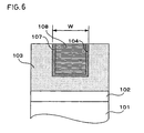
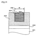
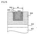
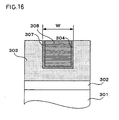
- FIG. 1 is an explanatory diagram schematically illustrating the procedure of fabrication and the configuration of the semiconductor device, (a) depicting the former half of the procedure of fabrication and (b) the latter half of the procedure of fabrication.
- a wiring 2 disposed in a semiconductor device 1 is composed, as illustrated in FIG. 1(b) , of an insulating film 3 containing silicon (Si), a wiring main body 8 formed of copper (Cu) (the mark in the parentheses denoting an atomic symbol) in an opening 4 disposed in the insulating film and shaped like a groove, and a barrier layer 7 formed between the wiring main body 8 and the insulating film 3.
- Si silicon
- Cu copper
- this barrier layer 7 is constructed as an Mn-based oxide coating having the atomic concentration of manganese (Mn) maximized in the central part in the direction of thickness.
- the barrier layer 7 contains Cu in the inner part thereof and the atomic concentration of Cu monotonously decreases from the side of the wiring main body 8 toward the insulating film 3 side opposite the wiring main body. Further, a divarent or trivalent ionized Mn exists on the side of the wiring main body 8 contiguous to the barrier layer 7.
- the fabrication of this semiconductor device 1, as illustrated in FIG. 1(a) comprises first forming an opening 4 of the shape of a groove in the Si-containing insulating film 3, then forming a copper alloy film (Cu alloy film) 5 containing manganese (Mn) and copper (Cu) on the inner peripheral surface of the opening 4, and subsequently embedding Cu in the opening 4 having formed the Cu alloy film 5, thereby forming a Cu-embedded layer 6. Then, by performing a heat treatment, it is rendered possible to have the Cu alloy film 5 integrated with the Cu of the Cu-embedded layer 6 and converted into the wiring main body 8 and as well have the barrier layer 7 ( FIG. 1(b) ) formed between the Cu alloy film 5 and the insulating film 3, with the result that the semiconductor device 1 provided with the wiring 2 will be completed.
- the heat treatment may be performed after the Cu alloy film 5 and the Cu-embedded layer 6 are formed as described above or at the stage of forming the Cu alloy film 5 prior to embedding the Cu.
- the heat treatment is performed at the stage of forming the Cu alloy film 5 prior to embedding the Cu, the surface side of the Cu alloy film 5 is converted by the heat treatment into a surface layer having Cu as a main component.
- the surface layer and the embedded Cu integrally form the wiring main body.
- the wiring configuration that is configured based on the Cu alloy film 5 may be formed on the insulating film having a flat surface. It can be utilized, in conjunction with a wiring groove (opening 4) opened for the sake of providing the insulating film 3 with a wiring or a hole perforated for the sake of enabling wirings to be mutually continued or connected, particularly effectively for forming a damascene type wiring. Now, the individual regions involved herein will be described sequentially.
- the insulating film 3 is a silicon dioxide (SiO 2 ) film containing Si and oxygen (O), a silicon oxide nitride (SiON) film, a silicon oxide fluoride (SiOF) film or a silicon oxide carbide (SiOC) film disposed on a silicon (Si) substrate, for example.
- This insulating film 3 may be formed as an insulating film in a multilayer wiring, namely as an interlayer insulation film.
- the insulating film 3 may be formed of a multilayer film having films of different materials stacked.
- the multilayer film may be composed of a silicon nitride (SiN) film and an SiO 2 film.
- SiN silicon nitride
- SiO 2 SiO 2 film.
- the surface layer of the insulating film 3 that contacts the Cu alloy film 5 is preferred to be a film containing Si and oxygen (O) as described above.
- the alloy elements contained in the Cu alloy film 5 used for coating the surface of the insulating film 3 are preferred to be such elements that possess larger diffusion coefficients in Cu than the Cu's own diffusion coefficient and allow large negative free energy for the formation of oxides.
- the elements of this description include manganese (Mn), zinc (Zn), germanium (Ge), strontium (St), silver (Ag), cadmium (Cd), tin (Sn), indium (In), barium (Ba), praseodymium (Pr) and neodymium (Nd), for example.
- these elements readily form oxides in the barrier layer 7 in combination with the oxygen of the insulating film 3 or the oxygen gas contained in a minute amount during the course of the heat treatment, impart to the barrier layer 7 an excellent barriering property against the diffusion of Cu from the wiring main body 8 side and enable the insulating film 3 to excel in the insulating property. They also impart to the barrier layer 7 an excellent barriering property against the diffusion of Si from the insulating film 3 side and enable the wiring main body 8 to acquire lowered resistance.
- a Cu-Mn alloy film may be cited, for example.
- the content of the element that forms an alloy with the Cu in the Cu alloy film 5 is preferred to be not less than 0.5% and not more than 20% in terms of atomic concentration.
- the Cu-Mn alloy film 5 containing Mn (Cu alloy film 5), for example, in this range of atomic concentration can be obtained by sputtering a target material formed of a Cu-Mn alloy containing Mn at an atomic concentration of 7%, for example.
- the Cu alloy film 5 can be formed on the insulating film made of SiO 2 , for example, by the high-frequency sputtering process. Further, it can be formed by physical deposition processes, such as the ion plating process and the laser ablation process. It can be also formed by an ordinary chemical vapor deposition (CVD) process. Irrespectively of the type of means to be adopted for this formation, the proper temperature for forming the Cu alloy film 5 on the insulating film 3 is not more than 100°C, preferably not more than 80°C.
- the excess will be at a disadvantage in suffering the oxidation reaction due to the contact with the underlying insulating film 3 to advance unduly conspicuously during the course of the formation of the film and consequently inducing difficulty in controlling the layer thickness during the formation of the barrier layer 7 in a small thickness.
- the formation of the film at a low temperature though serving to interfere with the advance of unwanted oxidation of the Cu alloy film (Cu-Mn alloy film, for example), proves unfavorable because the difference in thermal expansion coefficient between the insulating film 3 and the Cu alloy film 5 eventually induces separation of the Cu alloy film 5 from the insulating film 3.
- the temperature is preferred to be not less than -50°C and not more than +100°C, and more preferably not less than -20°C and not more than +80°C.
- the speed of coating the insulating film 3 with the Cu alloy film (Cu-Mn alloy film, for example) (the speed of depositing the film and the speed of growing the film) is preferred to be not less than 2 nanometers (unit: nm) per minute and not more than 300 nm per minute.
- the Cu alloy film 5 formed at a high speed exceeding 300 nm per minute turns out to be a film destitute of continuity because the internal texture thereof becomes disordered and generates voids copiously.
- the Cu alloy film 5 containing voids and lacking continuity entails a disadvantage in eventually failing to impart to the Cu alloy film 5 excellent adhesiveness with the insulating film 3 because the diffusion of Mn does not occur homogeneously and the presence of voids results in decreasing the area of contact of the insulating film 3 with the Cu alloy film 5.
- the Cu alloy film 5 formed at a low speed falling short of 2 nm per minute is fated to necessitate a heat treatment at a higher temperature for a longer time for the purpose of enabling the Mn contained in the Cu alloy film 5 to be dispersed toward the insulating film 3 side, though the inner texture is enabled to form a compact film.
- the barrier layer 7 formed in consequence of the heat treatment gains in thickness and eventually hinders the formation of a barrier film 7 of a small thickness in the wiring groove 4 having a small opening width.
- the formation of the Cu embedded layer 6 is accomplished by embedding Cu in the opening 4 that has formed the Cu alloy film 5 therein.
- the Cu can be deposited by various forming means, such as the electroplating, the CVD method and the high frequency sputtering method.
- the proper temperature for performing the heat treatment is not less than 150°C and not more than 600°C. If the heat treatment is performed at a lower temperature than 150°C, the shortage in temperature will be at a disadvantage in allowing no sufficient advance of the diffusion of an element forming the insulating film 3, such as Si, from the insulating film 3 to the barrier layer 7 side and consequently suffering a consequence of the barrier layer 7 deficient in adhesiveness with the insulating film 3 because the Si, for example, does not mingle in the barrier layer 7 so as to be thoroughly harmonized therewith.
- an element forming the insulating film 3 such as Si
- the heat treatment is advantageously carried out in a flow of a pure inert gas inevitably containing oxygen (O 2 ) only (such as an inert gas containing not more than 0.2 vol. ppm of oxygen, for example) or an inert gas containing 75 vol. ppm of oxygen in terms of volume concentration at most.
- Nitrogen gas or hydrogen gas can be used similarly to the inert gas because it is incapable of reacting Cu.
- the heat treatment therefore, may be carried out in a flow of nitrogen gas or hydrogen gas inevitably containing oxygen (O 2 ) only (such as nitrogen gas or hydrogen gas containing not more than 0.2 vol. ppm of oxygen, for example) or nitrogen gas or hydrogen gas containing 75 vol. ppm of oxygen in terms of volume concentration at most.
- This phenomenon occurs because the alloy element contained in the Cu alloy film 5 diffuses in the interface with the insulating film 3 and forms the barrier layer 7 and the alloy element not participating in the formation of the barrier layer 7 diffuses the Cu embedded layer 6 and forms on the surface of the wiring main body 8 an oxide by the reaction with the oxygen in the atmosphere of inert gas, nitrogen gas or hydrogen gas and consequently the alloy element concentration in the Cu alloy film decreases, becomes pure Cu of the same composition as the Cu embedded layer 6 and produces an integrated wiring main body 8 of low resistance.
- the heat treatment performed in the atmosphere of inert gas, nitrogen gas or hydrogen gas containing oxygen molecules in a volume ratio exceeding 75 vol. ppm is at a disadvantage in suffering the oxidation of the Cu alloy film 5 (such as a Cu-Mn alloy film, for example) and the Cu embedded layer 6 to be unfavorably promoted and consequently suffering the electric resistance of the wiring main body 8 to increase.
- the inert gas helium (He), neon (Ne), argon (Ar), krypton (Kr) and xenon (Xe) may be cited.
- He, Ne or Ar proves to be a preferable choice.
- the inert gas for forming the atmosphere is preferred to be Ar.
- nitrogen gas or hydrogen gas instead of the inert gas, it is rendered possible to perform the heat treatment at a lower cost.
- the Cu alloy film (such as Cu-Mn alloy film, for example) 5 reacts with the oxygen contained in the insulating film 3 and consequently forms the barrier layer 7 in the interface.
- the barrier layer 7 that is formed by the heat treatment performed at a prescribed temperature for a prescribed time has a decided thickness.
- the Cu alloy film 5 contains Mn copiously during the initial stage of growth, therefore, the part of Mn other than is spent in forming the barrier layer 7 remains in the Cu alloy film 5 and results in raising the resistance of the wiring main body 8. It is therefore necessary that the remaining Mn be expelled to the exterior and the resistance of the wiring be decreased.
- the wiring main body 8 is made to form an oxide on the surface thereof by using as the atmosphere for the heat treatment inert gas, nitrogen gas or hydrogen gas containing oxygen as an unavoidable impurity, or inert gas, nitrogen gas or hydrogen gas containing oxygen in a ratio of not more than 75 vol. ppm and enabling the excess Mn to react with the oxygen contained in the atmosphere.
- the Mn in the inner part of the wiring is dissipated from the inner part of the wiring main body 8 in the form of the surface oxides of the barrier layer 7 and the wiring main body 8 and the resistance of the wiring is equalized with that of pure Cu.
- the Mn in the Cu alloy film 5 reacts with the insulating film 3 and forms the barrier layer 7.
- the excess Mn other than is spent for forming the barrier layer 7 remains in the wiring unless the ensuing oxygen atmosphere is duly adjusted.
- the atmosphere of inert gas, nitrogen gas or hydrogen gas necessitates a trace of oxygen.
- the Cu of the wiring main body 8 will not be oxidized because the Mn is extracted from the wiring main body 8 and the Mn oxide is formed on the surface of the wiring main body 8. If the amount of oxygen is unduly large, however, the resistance of the wiring will be increased because not only Mn is oxidized but also Cu of the wiring main body 8 is oxidized.
- the Cu alloy film (such as Cu-Mn alloy film, for example) 5 and the Cu embedded layer 6 containing virtually no void and formed at the favorable depositing speed on the Si-containing insulating film 3 to the heat treatment performed in the advantageous atmosphere of inert gas, nitrogen gas or hydrogen gas in the aforementioned temperature range, it is rendered possible to distribute the Cu forming the Cu alloy film 5 so as to be monotonously decreased inside the barrier layer 7 toward the insulating film 3 side.
- the Cu alloy film (such as Cu-Mn alloy film, for example) 5 and the Cu embedded layer 6 containing virtually no void and formed at the favorable depositing speed on the Si-containing insulating film 3 to the heat treatment performed in the advantageous atmosphere of inert gas, nitrogen gas or hydrogen gas in the aforementioned temperature range, it is rendered possible to distribute the Si forming the insulating film 3 inside the barrier layer 7 so as to be monotonously decreased toward the Cu alloy film 5 side.
- the Cu alloy film (such as Cu-Mn alloy film, for example) 5 and the Cu embedded layer 6 containing virtually no void and formed at the favorable depositing speed on the Si-containing insulating film 3 to the heat treatment performed in the advantageous atmosphere of inert gas, nitrogen gas or hydrogen gas in the aforementioned temperature range, it is rendered possible to distribute the Mn atoms in the barrier layer 7 collectively in the region having the atomic concentrations of both Si and Cu approximately equal so as to have the largest atomic concentration in the barrier layer 7.
- the expression "approximately equal atomic concentrations" as used herein refers to the fact that the atomic concentrations of Cu and Si are equal or the fact that the atomic concentration of Si falls in the range of ⁇ 20% relative to the atomic concentration of Cu.
- the expression "collective distribution of Mn atoms” refers to the state having Mn locally distributed as illustrated on the right side of FIG. 1(b) .
- the distribution of the atomic concentration of an element can be investigated by the electron energy-loss spectroscopy (EELS) using an ordinary field emission transmission electron microscope.
- the Mn is distributed so as to possess the largest atomic concentration in the barrier layer 7 for the following reason. Specifically, since the oxide forming energy of Mn is lower than that of Cu and higher than that of Si, the Mn diffuses to the interface, reacts with the oxygen in SiO 2 , and forms an oxide. At this time, since Mn characteristically forms a composite oxide containing Cu and Si, it assumes the form of Mn oxide incorporating Cu on the wiring main body 8 side near the interface (barrier layer 7) and the form of Mn oxide incorporating Si on the other insulating layer 3 side.
- the occurrence of a balanced electric field in the region in the barrier layer 7 having the atomic concentrations of Cu and Si approximately equal due to the balance of the concentrations of Cu atoms and Si atoms may be one cause for concentrated distribution of the Mn atoms in that region.
- the concentrated distribution of Mn in this specific region in the barrier layer 7 can be obtained as a result of using the Cu alloy film 5 that permits uniform occurrence of the diffusion of Mn atoms owing to the deposition at the favorable speed of deposition and the consequent substantial absence of voids.
- the Mn atoms distributed in a concentrated manner in the region in the barrier layer 7 having the atomic concentrations of Cu and Si approximately equal possess an effect of preventing simultaneously the further diffusion of Cu from the wiring main body 8 side toward the insulating film 3 side and the further diffusion of Si from the insulating film 3 toward the wiring main body 8 side. They are furthermore capable of bringing about an effect of suppressing simultaneously the degradation of the electric insulating property of the insulating film 3 due to the penetration into the insulating film 3 of the Cu diffused from the wiring main body 8 and the impartation of high resistance to the wiring main body 8 due to the diffusion into the wiring main body 8 of the Si forming the insulating film 3.
- the thickness of the barrier layer 7 will be described below. As the ratio of the thickness of the barrier layer 7 to the horizontal width (opening width) W of the wiring groove 4 increases, the increase proportionately adds to the disadvantage incurred in forming the wiring main body 8 of low resistance. As the thickness of the barrier layer 7 formed in the wiring groove 4 of certain opening width increases, the volume of the wiring main body 8 decreases and the resistance of the wiring main body 8 increases proportionately.
- the thickness of the barrier layer 7 containing Cu, Mn and Si is specified to be not less than 1 nm and not more than 1/5 of the opening width W (refer to FIG. 1 ) of the wiring groove 4 formed in the insulating film 3 and as well the thickness of the barrier layer 7 to be not more than 10 nm at most. If the barrier layer 7 is an extremely thin film having a thickness falling short of 1 nm, this shortage will in the first place pose a problem of keeping the layer from becoming a barrier layer capable of sufficiently preventing the diffusion of Cu and Si.
- the thickness of the barrier layer increases beyond 1/5 of the opening width W of the wiring groove 4 or if it exceeds 10 nm though not exceeding 1/5 (such as when the thickness of the barrier layer 7 is 15 nm (1/6) while the opening width W is 90 nm, for example)
- the barrier layer 7 has too large a thickness to allow formation of the wiring main body 8 having a large width (large volume)
- the excess will entail a disadvantage in rendering difficult the formation of the wiring main body 8 of low resistance such as, for example, the wiring main body 8 formed of Cu having such a small specific resistance of about 2 ⁇ cm as equals that of pure Cu.
- the thickness of the barrier layer 7 is preferred to decrease in accordance as the opening width W of the wiring groove 4 is narrowed for the purpose of enabling the produced wiring main body 8 to acquire low resistance.
- the barrier layer 7 having a thickness of 5 nm to 10 nm is formed.
- the barrier layer 7 having a thickness of 7 nm ⁇ 3 nm is formed.
- the barrier layer 7 having a thickness of 5 nm ⁇ 2 nm is formed.
- the barrier layer 7 having a thickness of 3.5 nm ⁇ 1 nm is formed.
- the barrier layer 7 containing Cu, Mn and Si and having a thickness befitting the opening width W of the wiring groove 4 is formed by the heat treatment of the Cu-Mn alloy film 5 during the formation of the wiring of the Damascene structure that is provided with the barrier layer 7, the barrier layer 7 of the thickness mentioned above is formed by performing the heat treatment for a time (t: t > 0) that is decided by the logarithm-containing relation as shown by the following formula (1).
- x denotes the expected thickness (unit: nm) of the barrier layer 7
- k the proportionality constant relating to the time of heat treatment
- t the time of heat treatment (unit: hour)
- C the constant (unit: nm) relating to the temperature of heat treatment (unit: °C)
- the proportionality constant k and the constant C shown in Formula (1) when the heat treatment is performed in the same environment, assume smaller values than any other as shown in Formulae (2) and (3) in accordance as the temperature of the heat treatment is lowered. No matter what temperature may be used for the heat treatment, this temperature is preferred to decrease in proportion as the thickness in which the barrier layer 7 is formed decreases. When the heat treatment is performed at a fixed temperature, the time of the heat treatment is preferred to increase for the purpose of enabling the produced barrier layer 7 to acquire as large a thickness as permissible.
- this temperature is retained over a period of one hour. Then, for the purpose of obtaining the barrier layer 7 having a thickness of 3 nm by the heat treatment at 350°C, for example, this temperature is retained over a period of one hour. Then, for the purpose of obtaining the barrier layer 7 having a thickness of 2 nm by the heat treatment at 250°C, for example, this temperature is retained over a period of three hours.
- time of heat treatment refers to the interval from the time the temperature reaches the level for performing the heat treatment till the time the cooling is started.
- the time of heat treatment at the temperature of heat treatment in the preferred range mentioned above is generally preferred to be 60 minutes or more than that. Even in the heat treatment lasting over a long time, such as 100 hours or 200 hours, the thickness of the barrier layer 7 to be formed increases in proportion as the aforementioned value of logarithm of the time of heat treatment increases. In consideration of the economy of the process of heat treatment, however, the time of heat treatment is preferred to be 10 hours at most.
- the amorphous barrier layer 7 Since the barrier layer 7 is amorphous, i.e. devoid of grain boundaries serving as preferential routes for ready mutual diffusion of the component atoms of the insulating film 3 and the wiring main body 8 disposed on the opposite sides thereof, it proves advantageous for the sake of securing the barrier property.
- the proper temperature of heat treatment during the formation of the barrier layer is not less than 150°C and not more than 600°C as described above.
- the temperature of heat treatment is preferred to be not less than 150°C and not more than 450°C.
- the barrier layer 7 possessing a polycrystalline texture and containing grain boundaries copiously is obtained as a result, though the thermal diffusion of the Mn, for example, in the Cu alloy film 5 toward the insulating film 3 is promoted.
- this heat treatment likewise proves to be disadvantageous because atomic diffusion is generated via grain boundaries to induce loss of the barrier property against diffusion and the element diffused and mingled in the insulating layer entails leakage of the device operating current in the insulating film that is expected to enable mutual isolation of the adjacent wirings.
- the Mn of the Cu alloy film 5 migrates to the interface between the Cu alloy film 5 and the insulating film 3 and as well enables formation of the amorphous barrier layer 7.
- the ionized Mn begins to exist as described above on the wiring main body 8 side contiguous to the barrier layer 7 and electric fields are formed on either side of the barrier layer 7 that is in the process of being formed.
- the speed of the growth of the barrier layer 7 becomes proportionate to the logarithm of time.
- the thickness of the barrier layer 7 suddenly increases during the initial stage of formation and the speed of change of the thickness is slowed with the elapse of time.
- the amorphous barrier layer can be stably formed and, owning to the amorphousness, the barrier layer 7 consequently obtained is enabled to excel in the diffusion barrier property and the electric insulating property.
- the heat treatment is performed at a high temperature, such as 450°C, for a long time, such as 100 hours, the amorphous barrier layer 7 can be stably formed and the diffusion barrier property and the electric insulating property can be maintained.
- the Mn ionized to divalency or trivalency begins to exist on the wiring main body 8 side contiguous to the barrier layer 7.
- a positive electric charge exists on the wiring main body 8 side contiguous to the barrier layer 7, an electric field is formed between the barrier layer 7 and the insulating film 3 side opposed thereto, and the wiring main body 8 and the insulating film 3 are attracted to the barrier layer 7 by the electric fields formed on either side of the barrier layer 7. Even from this point of view, it is enabled to bring about the effect of enhancing the adhesiveness of the interface.
- the barrier layer 7 By performing the deposition at a comparatively high speed within the favorable range of deposition speed (2 nm/min to 300 nm/min) and thereafter performing the heat treatment at a comparatively low temperature within the favorable range of temperature (150°C to 450°C), it is rendered possible to form the barrier layer 7 having an amorphous texture. It is further rendered possible to form the barrier layer 7 that has Mn atoms centralized at a high concentration of not less than twice the atomic concentration of Cu or Si in the region of the inner part of the amorphous barrier layer 7 having the Cu atoms diffused from the Cu alloy film 5 approximately equal the concentration of the Si atom contained in the insulating film 3.
- the amorphous barrier layer 7 having the atomic concentrations of Cu, Si and Mn in the aforementioned relation is stably produced by depositing the Cu alloy film 5 at a depositing speed of not less than 7 nm and not more than 300 nm per minute on the insulating film 3, forming the Cu embedded layer 6 on the Cu-Mn alloy film 5 and thereafter heating the Cu-Mn alloy film 5 and the Cu embedded layer 6 in an atmosphere formed of pure inert gas, nitrogen gas or hydrogen gas and containing oxygen inevitably or in an atmosphere formed of inert gas, nitrogen gas or hydrogen gas and containing oxygen at a ratio of 75 vol. ppm at most at a temperature of not less than 150°C and not more than 450°C.
- the diffusion of Cu and Si can be suppressed more effectively owing to the action manifested by the oxide having Mn as a main component toward preventing the diffusion of Cu and Si. Then, by causing centralized distribution in the same region of the Mn atoms having a concentration of not less than twice the concentration of the Cu atoms or the Si atoms, the diffusion of Cu and Si can be prevented more thoroughly.
- the amorphous barrier layer having no grain boundary can be stably formed and the anomalous diffusion of Cu and Si via the grain boundary can be prevented.
- the question whether the barrier layer 7 is in the amorphous form or not can be determined by the electron diffraction pattern.
- the heat treatment may be performed after the formation of the Cu alloy film 5.
- the heat treatment may be carried out after the Cu embedded layer 6 has been embedded in the wiring groove 4 and then the surface of the Cu embedded layer 6 has been subsequently flattened by the CMP (chemical mechanical polishing).
- the barrier layer 7 is formed based on the Cu alloy film 5 that is formed by the method of sputtering a target material
- the barrier layer 7 of the construction contemplated by this invention can also be formed based on a multilayered film that is configured by first depositing a Mn film on the insulating film 3 containing Si and then depositing a Cu film on the Mn film. It can be alternatively formed based on a multilayered film configured by first depositing a Cu film on the insulating film 3 containing Si and then depositing an Mn film on the Cu film.
- the barrier layer is obtained by forming the Cu embedded layer 6 on the multilayered film and subjecting them to the heat treatment and the barrier layer is obtained by subjecting the multilayered film to the heat treatment prior to forming the Cu embedded layer 6.
- Wiring main body 8 When the Cu alloy film 5 deposited at a speed found favorable and containing virtually no void is formed, further the Cu embedded layer 6 is formed by embedding Cu in the wiring groove 4 continuous to the Cu alloy film 5 by the ordinary high-frequency sputtering method, and thereafter they are subjected to the heat treatment, the wiring main body 8 is enabled to acquire wiring resistance approximately equaling that of pure Cu and the produced wiring main body 8 is enabled to acquire low resistance.
- the barrier layer 7 formed of an oxide containing Cu, Si and Mn is formed between the wiring main body 8 and the insulating film 3 and since this barrier layer 7 has the atomic concentration of Cu monotonously decreasing from the wiring main body 3 side toward the insulating film 3 side, the atomic concentration of Si monotonously decreasing from the insulating film 3 toward the wiring main body 8 side and the atomic concentration of Mn maximize in the region in which the atomic concentrations of Cu and Si become approximately equal, the barrier layer 7 becomes the layer of a thermally stable and structurally compact oxide.
- the barrier layer 7, therefore, assumes a structure effective for the sake of suppressing the diffusion, acquires an excellent barriering property against the diffusion of Cu from the wiring main body 8 side and enables the insulating film 3 to excel further in the insulating property. It eventually acquires an excellent barriering property against the diffusion of Si from the insulating film 3 side and enables the wiring main body 8 to exhibit still lower resistance.
- the semiconductor device by thus being provided with the wiring that exhibits low resistance and possesses the ability to prevent leakage of the operating current of the device, merits more lowered electric power consumption.
- the barrier layer 7 has the atomic concentration of Cu therein monotonously decrease from the side of the wiring main body 8 having Cu as a main component toward the insulating film 3 side, it enables enhancement of the adhesiveness thereof with the Cu film constituting the wiring main body 8 and allows the semiconductor device to excel in the reliability of operation over a long time because the atomic concentration distribution does not change abruptly between the barrier layer 7 and the wiring main body 8 having Cu as a main component and the concentration of Cu is continuously varied.
- the barrier layer 7 has the boundary face thereof with the insulating film 3 consist of an oxide mainly containing Si and Mn in consequence of the diffusion and the atomic concentration of Si in the barrier layer 7 monotonously decrease from the insulating film 3 toward the wiring main body 8 side.
- the Si composition distribution from the insulating film 3 describes a continuous pattern instead of a precipitous and discontinuous pattern in the boundary face with the barrier layer 7.
- the interfacial strength between the insulating film 3 and the barrier layer 7 can be increased and the adhesiveness with the insulating film 3 can be enhanced. Even from this point of view, the semiconductor device is enabled to excel in the reliability of the operation over a long time.
- the present technique can realize lowering the electric power consumption of the semiconductor device by lowering the resistance of the wiring main body 8 and enhancing the insulating property of the insulating film 3 and as well enables the semiconductor device to excel in the reliability of operation over a long time by enhancing the adhesiveness between the barrier layer 7 and the wiring main body 8 and enhancing the adhesiveness between the barrier layer 7 and the insulating film 3.
- the present technique causes the atomic concentration of Mn in the region, in which the atomic concentrations of Cu and Si are approximately equal, to become not less than twice as high as the atomic concentration of Cu or Si.
- the barrier layer 7, therefore, becomes an oxide having Mn as a main component and the growth of this barrier layer 7 conforms to the law of logarithms of the time in contrast to the oxide that has Cu or Si as a main component and consequently continues to grow continuously.
- This conformity to the law of logarithms may be possibly described by the following supposition. Since the oxide of the barrier layer 7 having Mn as a main component possesses a compact structure and generates slow diffusion, the growth of this oxide is not induced by the ordinary thermal diffusion.
- the free electrons accompanying the Mn atoms are tunnel-transferred to the side opposite the barrier layer 7 (the insulating film 3 side) to bring about the presence of the ionized Mn on the wiring main body 8 side contiguous to the barrier layer 7, with the result that electric fields will be formed on either side of the barrier layer 7 in the process of formation.
- the acceleration of the diffusion of Mn ions in the barrier layer 7 that is caused by the electric fields initiates the growth of the oxide having Mn as a main component. Owing to this behavior of growth, the speed of the growth of the barrier layer 7 is made to conform to the law of logarithms.
- the thickness of the barrier layer rapidly increases during the initial stage of the formation of the barrier layer 7, the speed of change of the thickness is slowed with the elapse of time, and the growth is suppressed and prevented from exceeding several nm.
- the barrier layer 7, therefore, becomes a coating formed of a thermally stable and structurally compact Mn oxide and constitutes a structure effective for the sake of suppressing the diffusion.
- the barrier property of the barrier layer 7 against the diffusion of Cu from the wiring main body 8 side and the diffusion of Si from the insulating film 3 side can be further enhanced and the insulating property of the insulating film 3 and the capacity of the wiring to lower resistance can be further enhanced.
- the present technique can ensure the barrier property of the barrier layer 7 against the diffusion of Cu from the wiring main body 8 side and the diffusion of Si from the insulating film 3 side because it enables the barrier layer 7 to secure a thickness of not less than 1 nm or not more than 1/5 of the groove width of the opening.
- it can infallibly prevent such harmful effects as causing the wiring main body 8 to be narrowed by the barrier layer 7 and consequently adding to the effective electric resistance of the wiring because the thickness of the barrier layer 7 is set to be 10 nm at most. It, therefore, enables the insulating film 3 to acquire the insulating property and the wiring to acquire the capacity to lower resistance with greater infallibility.
- the present technique can suppress the anomalous diffusion of Cu and Si via the grain boundary because it has the barrier layer 7 formed in an amorphous state. It, therefore, can enhance the barrier property of the barrier layer 7 and can infallibly retain the insulating property of the insulating film 3 and the capacity of the wiring to lower resistance.
- the present technique allows the presence of a positive electric charge on the wiring main body 8 side adjoining the barrier layer 7 and enables formation of electric fields between the wiring main body and the insulating film 3 side opposite thereto across the barrier layer 7 because of the presence of Mg ionized to a divalent or trivalent on the wiring main body 8 side adjoining the barrier layer 7. Since the electric fields formed on either side of the barrier layer 7 attract the wiring main body 8 and the insulating film 3 toward the barrier layer 7, the effect of enhancing the adhesiveness of the grain boundary can be attained and the semiconductor device can be rendered excellent in the reliability of operation over a long time.
- the present technique allows the alloy elements, such as Mn, that have shunned the formation of the barrier layer 7 and have diffused and migrated as far as the surface of the wiring main body 8 to be oxidized with a minute amount of oxygen contained properly in the inert gas, nitrogen gas or hydrogen gas and dissipated from the interior of the wiring main body in the form of the surface oxide of the wiring main body 8 because the heat treatment is carried out in a pure inert gas, nitrogen gas or hydrogen gas inevitably containing oxygen or in an inert gas, nitrogen gas or hydrogen gas containing oxygen at a ratio of 75 vol. ppm at most.
- the resistance of the wiring approximately equals that of pure Cu and the wiring main body 8 having low resistance can be obtained.
- the present technique can bring about such various effects as lowering the resistance of the wiring main body 8, enhancing the insulating property of the insulating film 3 and enhancing the adhesiveness of the wiring main body 8 and the insulating film 3, because it contemplates performing the heat treatment at a temperature of not less than 150°C and not more than 600°C and imparting to the barrier layer 7 a structure peculiar to this technique.
- the present technique can stably form the barrier layer 7 in an amorphous state because it contemplates performing the heat treatment at a temperature of not less than 150°C and not more than 450°C.
- the wiring that is provided with the wiring main body 8 of low resistance and the insulating film 3 excelling in insulating property can be effectively utilized as a wiring for constructing various semiconductor devices.
- the barrier layer 7 having the atomic concentrations of Cu, Mn and Si distributed as disclosed herein can function satisfactorily as a barrier layer in spite of small thickness unlike the conventional technique that necessitates the formation of a thick barrier layer from a Ta-based material. Thus, it can be utilized for constructing a wiring for a silicon LSI that requires the width of wiring to be decreased to not more than 90 nm, for example, for enabling high-density integration.
- the wiring is provided with the wiring main body 8 of low resistance and as well the barrier layer 7 capable of preventing diffusion of Cu and Si so as to favor the prevention of the leakage of the device operating current, it can be utilized for constructing a wiring for a power device made of silicon or silicon germanium (SiGe) mixed crystal required to allow the flow of a large device operating current.
- the wiring structure is provided with the barrier layer 7 capable of avoiding the leakage of the device operating current and, therefore, can be advantageously utilized for constructing an electronic device of low electric power consumption.
- the barrier layer 7 capable of avoiding the leakage of the device operating current and, therefore, can be advantageously utilized for constructing an electronic device of low electric power consumption.
- it can be utilized for constructing a wiring for electronic display devices, such as a flat display panel (FDP), organic electroluminescence (EL) device and inorganic EL device, and photovoltaic cells, such as a solar cell.
- Example 1 will be described by way of a simple configuration for forming a flat Cu-Mn alloy film on a flat insulating film.
- the choice of the flat simple configuration was intended to enable more accurate determination of the electric resistivity of the formed Cu layer.
- FIG. 2 is a cross section illustrating the state of stacking prior to a heat treatment in Example 1
- FIG. 3 is a cross section illustrating the state of stacking subsequent to the heat treatment in Example 1.
- the Mn atoms were diffused and extracted toward the surface layer side of the Cu-Mn alloy film 105m, the Cu-Mn alloy film 105m was transformed into a Cu layer 108m occupied wholly by Cu, and an Mn oxide film 109m was formed on the surface layer of the Cu layer 108m.
- This Cu layer 108m that corresponded to the wiring main body 8 involved in the first embodiment was formed of substantially pure Cu.
- the Cu-Mn alloy film 105m was composed of 96% of Cu and 4% of Mn in terms of atomic concentration ratio and formed in a thickness of 150 nm.
- the barrier layer 107m acquired a thickness of 3 nm and the Mn oxide film 109m a thickness of 14 nm.
- the heat treatment used an atmosphere of argon (Ar) gas, i.e. an inert gas.
- argon (Ar) gas i.e. an inert gas.
- the samples of the Cu layer 108m obtained by performing the heat treatment at 350°C in the atmosphere having the volume content of oxygen in the argon gas varied were found to have varying magnitudes of specific resistance as shown in FIG. 4 .
- the abscissa axis is the scale of the time of heat treatment (unit: second) and the ordinate axis the scale of the specific resistance (unit: ⁇ cm).
- the curves represent the magnitudes of specific resistance shown by the samples of the Cu layer 108 formed by the heat treatment performed under varying gas atmosphere conditions A to D.
- A denotes an argon gas atmosphere containing oxygen at a volume content of 50 ppm
- B an argon gas atmosphere of high purity
- C an argon gas atmosphere containing oxygen at a volume content of 1000 ppm
- D a vacuum (here, 6.7 x 10 -5 Pa (5 x 10 -7 Torr)).
- the argon gas atmosphere of high purity denoted by B inevitably contained oxygen in a volume content of 0 to 0.2 ppm as shown in Table 1 below.
- G1 product standards of high-purity argon gas
- G2 G3 Purity >99.999 vol. % >99.995 vol. % >99.999 vol. % N 2 ⁇ 0.3 vol. ppm ⁇ 0.5 vol. ppm - O 2 ⁇ 0.1 vol. ppm ⁇ 0.2 vol. ppm ⁇ 0.2 vol. ppm H 2 ⁇ 0.1 vol. ppm ⁇ 0.5 vol. ppm ⁇ 1.0 vol. ppm Impurity CO ⁇ 0.1 vol. ppm ⁇ 0.2 vol.
- FIG. 4 clearly shows that the heat treatment performed in an argon gas atmosphere containing oxygen in a volume concentration of 50 vol. ppm (gas environment condition A) enabled the formation of the barrier layer 107m possessing atomic concentration distributions of Cu, Mn and Si conforming to this technique and as well that the specific resistance of the Cu layer 108m rapidly decreased in several minutes and reached a small magnitude of about 2.0 to 2.2 ⁇ cm in about 30 minutes, i.e. a level nearly equal to that of pure Cu (the electric resistivity of a thin film made of pure Cu: 1.9 to 2.0 ⁇ cm).
- the big decrease of the specific resistance of the Cu layer 108m in the gas environment condition A may be logically explained by a supposition that the Mn present in the Cu-Mn alloy film 105m was diffused to the surface of the Cu layer 108m, allowed to form the Mn oxide film 109m, and expelled from within the Cu layer 108m.
- the big decrease of the specific resistance of the Cu layer 108m in the gas atmosphere condition B may be logically explained by a supposition that because of extremely low oxygen concentration in the atmosphere, the Cu layer 108m, while expelling the Mn, could further suppress the oxidation induced in the Cu layer 108m by the largeness of the amount of oxygen in the condition A.
- the specific resistance of the Cu layer 108m decreased during the initial stage of the reaction treatment but increased thereafter because of vigorous surface oxidation.
- the specific resistance of the Cu layer 108m decreased during the initial stage of the heat treatment similarly to the condition C, it did not subsequently decrease but approximately leveled off or moderately increased because of the influence of the slow surface oxidation in the vacuum.
- FIG. 5 schematically illustrates the cross-sectional structure of the interior of the wiring groove in the state resulting from depositing the Cu-Mn alloy film on the insulating film and then depositing the Cu embedded layer thereon.
- FIG. 6 schematically illustrates the cross-sectional structure of the interior of the wiring groove in the state resulting from subjecting the Cu-Mn alloy film in the wiring groove and the Cu embedded layer to the heat treatment.
- FIG. 7 is a transmission electron micrograph illustrating the cross-sectional structure of the barrier layer formed by the heat treatment.
- a SiO 2 layer of a thickness of 150 nm was deposited by the ordinary chemical vapor deposition method as an insulating film 103.
- part of the insulating film 103 was removed by etching in accordance with the ordinary photolithographic technique to form a wiring groove (opening) 104.
- the wiring groove 104 had an opening width (lateral width) W of 90 nm.
- a Cu-Mn alloy film 105 was deposited on the surface of the insulating film 103 and the lateral faces and the bottom face of the interior of the wiring groove 104.
- the Cu-Mn alloy film 105 was formed by the ordinary high-frequency sputtering method using a target material formed of a Cu-Mn alloy containing Mn at an atomic concentration of 7%.
- the Cu-Mn alloy film 105 was formed while the temperature of the silicon substrate 101 was kept at 50°C.
- the depositing speed of the Cu-Mn alloy film 105 on the surface of the insulating film 103 was fixed at 12 nm per minute.
- the ratio of the atomic concentration of Mn in the Cu-Mn alloy film 105 was determined by the EELS method to be 5%.
- the thickness of the Cu-Mn alloy film 105 was such as to measure 80 nm on the flat surface 103a of the insulating film 103 that had avoided forming the wiring groove 104. By this time, the Cu-Mn alloy film of about 20 nm had been formed on the bottom of the wiring groove 104.
- the surface of the Cu-Mn alloy film 105 was plated with Cu by the ordinary electrolytic plating method (not shown in FIG. 5 ).
- the Cu plating was deposited in a thickness large enough to fill up the interior of the wiring groove 104.
- the ordinary CMP means was used to polish and remove the plated Cu layer and the Cu-Mn alloy film 105 till the flat surface 103a of the insulating film 103 was exposed.
- the Cu-Mn alloy film 10 was allowed to remain only inside the wiring groove 104 and the Cu deposited by plating on that surface was made to remain as a Cu embedded layer 106.
- the Cu-Mn alloy film 105 retained inside the wiring groove 104 and the Cu embedded layer 106 were subjected to the heat treatment performed in an argon (Ar) atmosphere containing oxygen at a volume ratio of 50 vol. ppm at a temperature of 300°C for 30 minutes.
- the Cu-Mn alloy 105 thermally diffused the Mn atoms contained therein toward the interface with the insulating film 103. Consequently, a barrier layer 107 was formed in a region near the interface.
- the formed barrier layer 107 had a thickness of 5 nm.
- the barrier layer 107 was analyzed by the electron energy-loss spectroscopy (EELS) to determine the concentration distribution of Cu, Mn and Si.
- EELS electron energy-loss spectroscopy
- This EELS analysis was performed with a field-emission transmission electron microscope (TEM) of high resolution, with the field scanned with electron beams spaced 0.2 nm apart.
- TEM field-emission transmission electron microscope
- the result of this analysis showed that the concentration of Cu atoms decreased monotonously from the wiring main body 108 toward the SiO 2 insulating film 103. It was also shown that the concentration of Si atoms decreased monotonously from the SiO 2 insulating film 103 toward the wiring main body 108.
- the Mn atoms were concentrically accumulated in the region in which the concentrations of Cu atoms and Si atoms are approximately equal. Then, the concentration of the accumulated Mn atoms was maximized in the region in which the concentrations of the Cu atoms and the Si atoms of the barrier layer 107 occupy approximately the same amount.
- the surface layer part of the Cu-Mn alloy film 105 that allowed expulsion of the Mn by diffusion and that was eventually occupied substantially wholly by Cu and the Cu embedded layer 106 were integrated to give rise to the wiring main body 108 formed of Cu and as well the Mn oxide film was formed on the surface layer part of the wiring main body 108 (not shown in FIG. 6 ).
- the oxide film in the upper surface layer part was removed by the CMP means. Consequently, the surface of the Cu wiring main body 108 was exposed and the Cu wiring main body 108 was tested for electric resistivity.
- the electric resistivity of the Cu wiring main body 108 was extremely low and reached 2.5 ⁇ cm, i.e. a level approximately equal to that of the wiring formed by embedding pure Cu in the wiring groove having an opening width of 90 nm.
- the barrier layer 107 effective for suppressing diffusion allowed the production of the Cu wiring exhibiting as low resistance as the wiring formed of pure Cu. Further, the barrier layer 107 enabled the insulating film 103 to gain an enhanced insulating property, the produced wiring to exhibit low resistance and acquire an ability to prevent leakage of the device operating current, and consequently the produced semiconductor device to have the benefit of low power consumption. Owing to the enhanced adhesiveness between the barrier layer 107 and the wiring main body 108 and the enhanced adhesiveness between the barrier layer 107 and the insulating film 103, the semiconductor device was enabled to excel in the reliability of operation for a long time.
- Example 3 Another technique will be described below citing, for example, the case of forming a wiring structure by using an amorphous barrier layer containing Cu, Mn and Si.
- the speed of depositing the Cu-Mn alloy film on the SiO 2 insulating film was set at 10 nm per minute.
- the Cu-Mn alloy film was heat-treated at 200°C for the purpose of forming an amorphous barrier layer devoid of a grain boundary capable of inducing normal diffusion of Mn.
- the atmosphere used for the heat treatment was an argon (Ar) atmosphere containing oxygen at a volume ratio of 50 vol. ppm similarly to the case of Example 2 above.
- the time of heat treatment was fixed at 4 hours. Consequently, the barrier layer having a thickness of 3 nm was formed.
- FIG. 8 illustrates the result of analysis obtained by the electron energy-loss spectroscopy (EELS) regarding the distribution of elements in the amorphous barrier.
- EELS electron energy-loss spectroscopy
- the Mn atoms were concentrically accumulated in the region in which the concentrations of the Cu atoms and the Si atoms occupy approximately the same amount.
- the concentration of the Mn atoms accumulated in that region reached 33 atom %, i.e. well over twice these concentrations.
- the electric resistivity of the Cu wiring main body formed based on the Cu embedded layer was extremely low and reached 2.4 ⁇ cm, i.e. a level approximately equaling that of the wiring formed by embedding pure Cu in the wiring groove having an opening width of 90 nm.
- Example 3 similarly to Example 2, the amorphous barrier layer more effective for suppressing diffusion allowed the production of the Cu wiring exhibiting as low resistance as the wiring formed of pure Cu. Further, the barrier layer enabled the insulating film to gain an enhanced insulating property, the produced wiring to exhibit low resistance and acquire an ability to prevent the leakage of the device operating current, and consequently the produced semiconductor device to have the benefit of low power consumption. Owing to the enhanced adhesiveness between the barrier layer and the wiring main body and the enhanced adhesiveness between the barrier layer and the insulating film, the semiconductor device was enabled to excel in the reliability of operation for a long time.
- Example 4 Another technique will be described in detail below citing, for example, the case of forming the wiring structure from the multilayered film of Mn film and Cu film deposited on the Si-containing insulating film.
- the multilayered film formed of Cu film and Mn film and the Cu embedded layer were heat-treated at 350°C.
- the atmosphere used for this heat treatment was an argon (Ar) atmosphere containing oxygen at a volume ratio of 60 vol. ppm.
- the time of heat treatment was fixed at 4 hours. Consequently, the barrier layer having a thickness of 3 nm was formed.
- the barrier layer containing Cu, Mn and Si was analyzed by the EELS method with a view to determining the distribution of the component elements therein, it was confirmed that the atomic concentration of Cu decreased monotonously from the Cu-Mn alloy film toward the SiO 2 -SiOF multilayered insulating film side. Meanwhile, the atomic concentration of Si decreased monotonously, similarly to the case of the Cu atom, from the SiO 2 -SiO multilayered insulating film toward the Cu-Mn alloy film side.
- the Mn atoms were concentrically accumulated in the region approximating more toward the SiO 2 -SiOF multilayered insulating film than toward the center in the direction of thickness of the barrier layer wherein the concentrations of the Cu atoms and the Si atoms occupy approximately the same amount.
- the electric resistivity of the Cu wiring main body formed based on the Cu embedded layer was extremely low and reached 3.4 ⁇ cm, i.e. a level approximately equal to that of the wiring formed by embedding pure Cu in the wiring groove having an opening width of 45 nm.
- the barrier layer effective for suppressing diffusion allowed the production of the Cu wiring exhibiting as low resistance as the wiring formed of pure Cu. Further, the barrier layer enabled the insulating film to gain an enhanced insulating property, the produced wiring to exhibit low resistance and acquire an ability to prevent the leakage of the device operating current, and consequently the produced semiconductor device to have the benefit of low power consumption. Owing to the enhanced adhesiveness between the barrier layer and the wiring main body and the enhanced adhesiveness between the barrier layer and the insulating film, the semiconductor device was enabled to excel in the reliability of operation for a long time.
- Example 4 the heat treatment was performed at 350°C for 4 hours in an argon (Ar) atmosphere containing oxygen at a volume ratio of 60 vol. ppm. The same results as in Example 4 were obtained when the heat treatment was performed at 350°C for 4 hours in a nitrogen gas atmosphere containing oxygen at a volume ratio of 60 vol. ppm and in a hydrogen gas atmosphere containing oxygen at a volume ratio of 60 vol. ppm.
- Example 5 the wiring structure provided with a barrier layer was formed in the same manner as in Example 2, except changing only the conditions for the heat treatment.
- the heat treatment of the Cu-Mn alloy film and the Cu embedded layer was performed at 300°C for 90 minutes in an argon atmosphere inevitably containing oxygen at a ratio of 0.1 ppm only. Consequently, the Mn atoms contained in the Cu-Mn alloy film were thermally diffused from the alloy film toward the interface thereof with the insulating film 103, with the result that the barrier layer was formed in the region near the interface.
- the barrier layer thus formed had a thickness of 5 nm.
- the surface layer part of the Cu-Mn alloy film that allowed the expulsion of the Mn by diffusion and that was eventually occupied substantially wholly by Cu and the Cu embedded layer were integrated to give rise to the wiring main body formed of Cu.
- the barrier layer was analyzed by the electron energy-loss spectroscopy (EELS) to determine the distribution of the Cu, Mn and Si atoms in the layer.
- EELS electron energy-loss spectroscopy
- This EELS analysis was performed with a field-emission transmission electron microscope (TEM) of high resolution, with the field scanned with electron beams spaced 0.2 nm apart.
- TEM field-emission transmission electron microscope
- the Mn atoms were concentrically accumulated in the region in which the concentrations of Cu atoms and Si atoms are approximately concurred. Then, the concentration of the accumulated Mn atoms was maximized in the region in which the concentrations of the Cu atoms and the Si atoms of the barrier layer occupy approximately the same amount, to approximately twice the concentrations of Cu atoms and Si atoms.
- the electric resistivity was extremely low and reached 2.6 ⁇ cm, i.e. a level approximately equaling that of the wiring formed by embedding pure Cu in the wiring groove having an opening width of 90 nm.
- the barrier layer effective for suppressing diffusion allowed the production of the Cu wiring exhibiting as low resistance as the wiring formed of pure Cu. Further, the barrier layer enabled the insulating film to gain an enhanced insulating property, the produced wiring to exhibit low resistance and acquire an ability to prevent the leakage of the device operating current, and consequently the produced semiconductor device to have the benefit of low power consumption. Owing to the enhanced adhesiveness between the barrier layer and the wiring main body and the enhanced adhesiveness between the barrier layer and the insulating film, the semiconductor device was enabled to excel in the reliability of operation for a long time.
- Example 5 the heat treatment was performed at 300°C for 90 minutes in a pure argon gas atmosphere inevitably containing oxygen at a ratio of 0.1 ppm only. The same results as in Example 5 were obtained when the heat treatment was performed at 300°C for 90 minutes in a nitrogen gas atmosphere inevitably containing oxygen at a ratio of 0.1 ppm only and in a hydrogen gas atmosphere inevitably containing oxygen at a ratio of 0.1 ppm only.
- Example 6 the wiring structure provided with a barrier layer was formed in the same manner as in Example 2, except changing the opening width W of the wiring groove.
- Example 6 and Example 2 differ in the following points.
- the opening width W was fixed at 32 nm and the thickness of the Cu-Mn alloy film was such as to measure 30 nm on the flat surface of the insulating film that had avoided forming the wiring groove. By this time, the Cu-Mn alloy film of about 8 nm had been formed on the bottom of the wiring groove.
- the heat treatment for the Cu-Mn alloy film retained in the wiring groove and the Cu embedded layer was carried out at a temperature of 350°C over a period of 30 minutes in a pure argon atmosphere inevitably containing oxygen at a ratio of 0.1 ppm only.
- the Cu-Mn alloy film thermally diffused the Mn atoms contained therein toward the interface thereof with the insulating film, with the result that the barrier layer was formed in the region near the interface.
- the formed barrier layer had a thickness of 2 nm.
- Example 6 the barrier layer was analyzed by the electron energy-loss spectroscopy (EELS) to determine the concentration distributions of Cu, Mn and Si atoms therein.
- EELS electron energy-loss spectroscopy
- This EELS analysis was performed with a field-emission transmission electron microscope (TEM) of high resolution, with the field scanned with electron beams spaced 0.2 nm apart.
- TEM field-emission transmission electron microscope
- the result of this analysis showed that the concentration of Cu atoms decreased monotonously from the wiring main body toward the SiO 2 insulating film. It was also shown that the concentration of Si atoms decreased monotonously from the SiO 2 insulating film toward the wiring main body.
- the Mn atoms were concentrically accumulated in the region in which the concentrations of Cu atoms and Si atoms are approximately concurred. Then, the concentration of the accumulated Mn atoms was maximized in the region in which the concentrations of the Cu atoms and the Si atoms of the barrier layer occupy approximately the same amount, to about twice the concentrations of the Cu atoms and the Si atoms.
- the transmission electron micrograph of the barrier layer that had undergone the heat treatment clearly shows that the barrier layer formed therein a random texture peculiar to amorphousness.
- the electron energy-loss spectroscopy (EELS) spectrua of Mn were obtained from the region of the wiring main body and the region of the barrier layer. They allowed confirmation that the Mn atoms existing in the region adjoining the barrier layer of the wiring main body possessed the same valency as in the central part of the barrier layer and that they were ionized to divalency or trivalency.
- EELS electron energy-loss spectroscopy
- the electric resistivity was extremely low and reached 4.6 ⁇ cm, i.e. a level approximately equaling that of the wiring formed by embedding pure Cu in the wiring groove having an opening width of 32 nm.
- the barrier layer effective for suppressing diffusion allowed the production of the Cu wiring exhibiting as low resistance as the wiring formed of pure Cu. Further, the barrier layer enabled the insulating film to gain an enhanced insulating property, the produced wiring to exhibit low resistance and acquire an ability to prevent the leakage of the device operating current, and consequently the produced semiconductor device to have the benefit of low power consumption. Owing to the enhanced adhesiveness between the barrier layer and the wiring main body and the enhanced adhesiveness between the barrier layer and the insulating film, the semiconductor device was enabled to excel in the reliability of operation for a long time.
- Example 6 has demonstrated that this technique can be applied to the case of the wiring groove having a narrower opening width of 32 nm besides the case of the wiring groove having an opening width of 90 nm or 45 nm.
- FIG. 9 is an explanatory diagram schematically illustrating the procedure of fabrication and the configuration of a semiconductor device, (a) depicting the former half of the procedure of fabrication and (b) the latter half of the procedure of fabrication.
- FIG. 9 the structural elements approximately identical with those of the first embodiment described above will be denoted by the same reference numerals and will be omitted from the description given herein.
- This example differs from the first embodiment in the construction of a barrier layer 7a.
- the barrier layer 7a as illustrated in the right side of FIG. 9(b) , is configured as an Mn-based oxide coat having the atomic concentration of Mn maximized in the central part in the direction of thickness and the barrier layer 7a contains Cu therein and the atomic concentration of the Cu decreases monotonously from the wiring main body 8 side toward the insulating film 3 side that is opposed to the wiring main body 8.
- Si is not indicated as a constructional element.
- the thickness of the barrier layer 7a is specified to be not less than 1 nm and not more than 1/5 of the opening width W (refer to FIG. 9(a) ) of the wiring groove 4 disposed in the insulating film 3 and not more than 10 nm as well.
- the Mn ionized to divalece or trivalence exists in the side of the wiring main body 8 contiguous to the barrier layer 7a.
- the heat treatment is carried out in the current of a pure inert gas inevitably containing only oxygen (O 2 ) or an inert gas containing oxygen in a volume concentration of 75 vol. ppm at most.
- a pure inert gas inevitably containing only oxygen (O 2 ) or an inert gas containing oxygen in a volume concentration of 75 vol. ppm at most.
- nitrogen gas or hydrogen gas inevitably containing oxygen (O 2 ) or nitrogen gas or hydrogen gas containing oxygen in a volume concentration of 75 vol. ppm at most.
- the barrier layer 7a has a simple structure as compared with that in the first embodiment and nevertheless can manifest the following effects similarly to the first embodiment.
- a barrier layer 7a formed of an Mn-based oxide and having the atomic concentration of Mn maximized in the central part of the layer thickness namely a barrier layer 7a formed of an Mn-based oxide and having Mn concentrated in the central part of the layer thickness, is interposed between the insulating film 3 and the wiring main body 8.
- This barrier layer 7a exhibits thermal stability, forms a structurally compact layer and constitutes an effective configuration for the sake of suppression of diffusion. Thus, it eventually acquires an excellent barriering property against diffusion of Cu from the wiring main body 8 side and enables the insulating film 3 to excel in the insulating property.
- the semiconductor device 1a aimed at, therefore, is enabled to merit low electric power consumption because of the provision of the wiring that exhibits low resistance and permits prevention of the leakage of the operating current of the device.
- the barrier layer 7a is made to be a Cu-containing coating, it is enabled to enhance the adhesiveness thereof with the Cu film fated to be formed contiguously with the surface of the barrier layer 7a and destined to constitute the wiring main body 8 and permit the semiconductor device 1a to excel in the reliability of operation over a long time because the atomic concentration distribution is not broken between the barrier layer 7a and the wiring main body 8 having Cu as a main component and the concentration of Cu is continuously varied.
- the atomic concentration of Cu in the barrier layer 7a is monotonously decreased from the side of the wiring main body 8 having Cu as a main component toward the insulating film 3 side, it is enabled to further enhance the adhesiveness thereof with the Cu film constituting the main body 8 of the wiring and permit the semiconductor deice 1a to excel in the reliability of operation over a long time because the atomic concentration distribution is not broken between the barrier layer 7a and the wiring main body 8 having Cu as a main component and the concentration of Cu is continuously varied.
- the Mn oxide becomes to exhibit slow diffusion and the barrier layer 7a is eventually formed of the oxide having the Mn as its main component because the barrier layer 7a is eventually made to assume Mn as its main component element and this Mn exhibits a strong binding force with oxygen.
- the barrier layer 7a therefore, exhibits an excellent barrier property against the diffusion of Cu from the wiring main body 8 side.
- this technique can ensure the barrier property of the barrier layer 7a against the diffusion of Cu from the wiring main body 8 side and the diffusion of Si from the insulating film 3 side because it enables the barrier layer 7a to secure a thickness of not less than 1 nm or not more than 1/5 of the groove width of the opening.
- it can infallibly prevent such harmful effects as causing the wiring main body 8 to be narrowed by the barrier layer 7a and consequently adding to the effective electric resistance of the wiring because the thickness of the barrier layer 7a is set to be 10 nm at most. It, therefore, enables the insulating film 3 to acquire the insulating property and the wiring to acquire the capacity to lower resistance with greater infallibility.
- the technique can suppress the anomalous diffusion of Cu and Si via the grain boundary because it has the barrier layer 7a formed in an amorphous state. It, therefore, can enhance the barrier property of the barrier layer 7a and can infallibly retain the insulating property of the insulating film 3 and the capacity of the wiring to lower resistance.
- the technique contemplates performing the heat treatment in a pure inert gas inevitably containing oxygen or in an inert gas containing oxygen in a ratio of 75 vol. ppm at most. Therefore, the alloy elements, such as Mn, that have shunned formation of the barrier layer 7a and have diffused and migrated as far as the surface of the wiring main body 8, are oxidized with a minute amount of oxygen contained properly in the inert gas, allowed to form an oxide on the surface of the wiring main body 8 and dissipated from the interior of the wiring main body 8 in the form of a surface oxide of the wiring main body 8. As a result, the resistance of the wiring approximately equals that of pure Cu and the wiring main body having low resistance body can be obtained.
- the technique can bring about such various effects as lowering the resistance of the wiring main body 8, enhancing the insulating property of the insulating film 3 and enhancing the adhesiveness of the wiring main body 8 and the insulating film 3, because it contemplates performing the heat treatment at a temperature of not less than 150°C and not more than 600°C and imparting to the barrier layer a structure peculiar to the technique.
- the technique can stably form the barrier layer 7a in an amorphous state because it contemplates performing the heat treatment at a temperature of not less than 150°C and not more than 450°C.
- FIG. 10 is a schematic cross section illustrating the internal structure of a wiring groove (opening) in a state resulting from depositing a Cu-Mn alloy film and then depositing a Cu embedded layer.
- FIG. 11 is a cross section illustrating the structure of the inside of the wiring groove in a state resulting from subjecting the Cu-Mn alloy film and the Cu embedded layer in the wiring groove to heat treatment.
- FIG. 12 is a transmission electron micrograph of the cross section of the barrier layer.
- FIG. 13 is a diagram illustrating the state of ions of the Mn element in the wiring main body and the barrier layer.
- FIG. 14 shows the result of the chemical composition analysis performed on the barrier layer to determine Cu and Mn contents by the electron energy-loss spectroscopy (EELS).
- EELS electron energy-loss spectroscopy
- an insulating film 203 having a thickness of 150 nm, made of SiO 2 and intended as an interlayer insulation layer was formed by the ordinary chemical vapor deposition method on the surface of an electroconductive silicon semiconductor layer 202 formed on a silicon substrate 201, a wiring groove (opening) 204 was dug into the insulating film 203, and a Cu-Mn alloy film 205 was deposited on the lateral walls in the wiring grove 204 and on the surface thereof.
- the lateral width (opening width) W of the wiring groove 204 was 90 nm.
- the Cu-Mn alloy film 205 was formed by sputtering a target material made of Cu-Mn alloy containing Mn in an atomic concentration of 7% in an ordinary high-frequency sputtering device. By the EELS, the ratio of atomic concentration of Mn in the produced Cu-Mn alloy film 205 was determined to be about 5%. The thickness of the Cu-Mn alloy film 205 was such as to measure 80 nm when it was formed on the flat surface of an Si substrate.
- Cu was deposited on the surface of the Cu-Mn alloy film 205 by the electrolytic plating method while using as a seed layer the Cu-Mn alloy film 205 formed by the sputtering method, with the result that a Cu embedded layer 206 was formed in the wiring groove 204 (refer to FIG. 8 ).
- the structure provided inside the wiring groove 204 of the insulating film 203 with the Cu-Mn alloy film 205 and the Cu embedded layer 206 was heat-treated in an argon (Ar) atmosphere containing oxygen in a volume ratio of 25 vol. ppm at a temperature of 400°C over a period of 30 minutes.
- the rate of temperature increase from room temperature to the temperature of heat treatment, i.e. 400°C, was fixed at 8°C per minute.
- the average rate of temperature decrease from 400°C to room temperature after completion of the heat treatment was fixed at 10°C per minute.
- the Cu-Mn alloy film 205 thermally diffused the Mn atoms contained therein toward the interface thereof with the insulating film 203, with the result that a barrier layer 207 formed of an Mn-based oxide was formed in the region near the interface as illustrated in FIG. 11 .
- the barrier layer 207 formed by the heat treatment in the present example had a thickness of 5 nm.
- FIG. 12 The transmission electron micrograph of the barrier layer 207 subsequent to undergoing the heat treatment is shown in FIG. 12.
- FIG. 12 clearly shows that a random texture peculiar to amorphousness was formed in the barrier layer 207.
- the electron energy-loss spectroscopic (EELS) spectra of Mn were obtained from the regions a and b illustrated in FIG. 12 .
- the results of the analysis are shown in FIG. 13 .
- the region a adjoins the barrier layer 207 in a wiring main body 108 and the region b formed the central part of the barrier layer 207.
- the Mn spectrum from the region a was observed to possess a peak strength at the same energy position as the Mn spectrum from the central part of the barrier layer 207 of the region b. This fact allowed confirmation that the Mn present in the region adjoining the barrier layer 207 of the wiring main body 208 possessed the same valence as in the central part of the barrier layer 207 and was ionized to divalence or trivalence.
- the barrier layer 207 contained Cu in the interior thereof.
- the concentration of the Cu atoms was confirmed to decrease monotonously from the wiring main body 208 side toward the insulating film 203 side.
- FIG. 14 The results of the analysis of the barrier layer 207 conducted by the electron energy-loss spectroscopy (EELS) to determine the distribution of elements therein are shown in FIG. 14 .
- This EELS was performed using a field-emission transmission electron microscope of high resolution, with the field scanned with electron beams spaced 0.2 nm apart.
- the Mn concentration was maximized in the central part in the direction of thickness of the barrier layer 207.
- the EELS it was confirmed that the Cu concentration decreased monotonously from the side of the film (wiring main body 208) maid mainly of Cu toward the insulating film 203 (SiO 2 film) side. Further, the atomic concentration of Cu was less than the atomic concentration of Mn in the central part in the direction of thickness of the barrier layer 207.
- the Cu-Mn alloy film 205 that allowed expulsion of the Mn by diffusion and that was eventually occupied wholly by Cu and the Cu embedded layer 206 were integrated to give rise to the wiring main body 208.
- an Mn-based oxide coat was formed also on the surface layer part constituting the upper side of the wiring main body 208 (not shown in FIG. 11 ).
- the Mn-based oxide coat in the upper surface layer part was removed by the chemical mechanical polishing (abbreviation: CMP) method.
- CMP chemical mechanical polishing
- the surface of the Cu wiring main body 208 was exposed and then the Cu wiring main body 208 was tested for electric resistivity.
- the electric resistivity of the Cu wiring main body 208 was extremely low and reached 2.5 ⁇ cm, i.e. a level approximately equal to that of the wiring formed by embedding pure Cu in the wiring groove having an opening width of 90 nm.
- the amorphous barrier layer still more effective for suppressing diffusion enabled the production of the Cu wiring exhibiting low resistance approximating close to that of the wiring made of pure Cu.
- the barrier layer further enabled the insulating property of the insulating film to be enhanced, allowed the production of a wiring that had the benefit of low resistance and possessed the ability to prevent the leakage of the device operating current, and granted the semiconductor device low electric power consumption.
- the semiconductor device was enabled to excel in the reliability of operation over a long period of time.
- the Cu wiring of the construction conforming to this technique was endowed with low resistance convenient for the efficient flow of the device operating current and provided with an Mn-based oxide coat capable of sufficiently fulfilling the function as a barrier layer, it could avoid the leakage of the device operating current and could be favorably utilized for constructing the electronic device of low electric power consumption. It could be utilized for constructing electronic devices, such as liquid crystal display (LCD), flat display panel (abbreviation: FDP), organic electroluminescence (abbreviation: EL) device and inorganic EL device, for example.
- LCD liquid crystal display
- FDP flat display panel
- EL organic electroluminescence
- inorganic EL device for example.
- the Mn-based oxide coat possessing the distribution of atomic concentration of Mn disclosed above can function as the barrier layer in the form of a thin film without daring the formation of a barrier layer having a large thickness from the Ta-based material as observed heretofore and, therefore, can be utilized for constructing a silicon LSI having such a small wiring width as not more than 90 nm for the sake of enabling integration in a high density.
- the wiring conforming to this technique is composed of a wiring main body of low resistance and a barrier layer convenient for preventing leakage of the device operating current and, therefore, can be utilized for constructing a power device made of silicon or silicon germanium (SiGe) and required to flow a large device operating current.
- the sputtering target material that is used in depositing the Cu alloy film 5 on the insulating film 3 in the embodiments described above will be described.
- the composition of the Cu alloy film 5 formed by sputtering the sputtering target material and the composition of the used sputtering target material are approximately identical.
- the sputtering target material to be used for depositing the Cu alloy film 5 is composed of copper (Cu) as a main component and manganese (Mn) as an essential element.
- This target material contains the impurities that inevitably remain in Cu besides the essential component.
- the present inventor has found that the impurities inevitably contained in the sputtering target material entail the following disadvantages.
- This technique therefore, specifies the unavoidable impurities that entail the disadvantages enumerated above and prescribes rules for ensuring substantial exclusion of these impurities.
- the wiring main body formed from the sputtering target material therefore, enabled fabrication of a semiconductor device that had the benefit of low resistance, good conductivity and low electric power consumption.
- This sputtering target material is composed, as described above, of Cu as a main component, Mn as an essential element and the unavoidable impurities inevitably remaining in the residual Cu excluding the essential element.
- the content of Mn as the essential element is preferred to be not less than 0.5% and not more than 20% of the whole Cu alloy in terms of atomic concentration for the following reason. If this content falls short of 0.5%, the shortage will scarcely allow the formation of a barrier layer not more than I nm in thickness in part of the interface and will prevent the acquisition of diffusion-barrier property and adhesiveness of the interface because of the insufficient supply of Mn necessary for forming the barrier layer. If the content exceeds 20%, the excess will cause the barrier layer to acquire a thickness of not less than 10 nm and prevent the barrier layer from obtaining superiority to the barrier layer such as Ta prevailing at present.
- the essential element may be made to contain therein together with Mn at least one of the elements comprising zinc (Zn), germanium (Ge), strontium (Sr), silver (Ag), cadmium (Cd), indium (In), tin (Sn), barium (Ba), praseodymium (Pr) and neodymium (Nd), i.e. the elements fated to form a solid solution in Cu as the main component.
- the elements comprising zinc (Zn), germanium (Ge), strontium (Sr), silver (Ag), cadmium (Cd), indium (In), tin (Sn), barium (Ba), praseodymium (Pr) and neodymium (Nd), i.e. the elements fated to form a solid solution in Cu as the main component.
- These solid-solution elements possess diffusion constants equal to or larger than Cu's own diffusion coefficient and are more liable to oxidation than Cu and, therefore, enables the Mn-based oxide coat as the barrier layer to be improved in barriering property against Cu being diffused from the wiring main body side and in adhesiveness with the insulating film and as well enables the semiconductor device to acquire excellent reliability of operation over a long period of time.
- the unavoidable impurities consist of one of eight groups in a total content of not more than 0.1% as an atomic concentration based on the whole of the target material, the first group consisting of lithium (Li), the second group consisting of beryllium (Be), calcium (Ca) and magnesium (Mg), the third group consisting of boron (B), gallium (Ga) and aluminum (Al), the fourth group consisting of silicon (Si), the fifth group consisting of antimony (Sb), the sixth group consisting of principal transition metals including scandium (Sc), titanium (Ti), vanadium (V), chromium (Cr), iron (Fe), cobalt (Co), nickel (Ni), yttrium (Y), zirconium (Zr), niobium (Nb), molybdenum (Mo), technetium (Tc), ruthenium (Ru), palladium (Pd), hafnium (Hf), tantalum (Ta), tungsten (W), rhenium
- the sputtering target material ultimately augments the electric resistivity of the wiring main body vainly. It is directed to defining the concentrations of (a) an impurity element possessing large free energy for forming the oxide and exhibiting a high affinity with oxygen, (b) an impurity element whose diffusion coefficient in Cu is larger than Cu's own diffusion coefficient, (c) an impurity element forming an intermetallic compound with Cu and (d) an impurity element for forming an intermetallic compound with Mn.
- the concentration of the specific element that chemically reduces the interlayer insulation film 3 made of SiO 2 will be defined and the concentration of the element that raises the electric resistivity per 1% of Cu in terms of atomic concentration beyond 5 ⁇ cm will be defined.
- Lithium (Li) that constitutes the first group belongs to Group I in the periodic table of the elements.
- the sputtering target material does not contain this element. If it contains the element, the content thereof is preferred to be not more than 0.1 % in atomic concentration.
- the words "not contain” as used herein refer to the concentration that falls short of the minimum limit of detection from the standpoint of analysis.
- Group I elements particularly Li, exhibit large solid solubility in Cu, have an inclination to augment the electric resistivity of Cu (wiring main body 8) by remaining therein, and possess the possibility of suddenly decreasing the liquidus-line temperature in proportion to the increase of the Li concentration and inducing the exudation of liquid during the course of process.
- Beryllium (Be), calcium (Ca) and magnesium (Mg) that constitute the second group belong to Group II in the periodic table of the elements.
- the sputtering target material does not contain these elements. If it contains these elements, the total content of these elements is preferred to be not more than 0.1% as atomic concentration.
- the Be, Ca and Mg possess high reactivity with oxygen. If the sputtering target material contains these elements in a total atomic concentration exceeding 0.1%, the concentrations of the oxides containing these elements will increase conspicuously in the Cu alloy film 5. Since these oxides augment the electric resistivity of the Cu alloy, the Cu alloy film 5 convenient for producing the Cu film (wiring main body 8) of high conductivity will not be obtained eventually. Conversely, if the atomic concentrations of these individual elements are suppressed below 0.1%, the Cu alloy film advantageous for producing a Cu film (wiring main body 8) of high conductivity will be stably obtained and enabled to suppress the action of chemically reducing a compound, such as SiO 2 , which forms an interlayer insulation film 3.
- a compound such as SiO 2
- Boron (B), gallium (Ga) and aluminum (Al) constituting the third group belong to the Group III in the periodic table of the elements.
- the sputtering target material does not contain these elements. If it contains these elements, the total atomic concentrations of these elements are preferred to be not more than 0.1%.
- the atomic concentrations of the individual elements B, Ga and Al constituting the third group total not more than 0.1%, it will be rendered possible to obtain the Cu alloy film 5 capable of producing a Cu film (wiring main body 8) of high conductivity. Since the B, Ga and Al have larger free energy changes for the formation of oxides or larger enthalpy changes than the Si oxides, for example, they exhibit higher degrees of reactivity with oxygen. If oxides containing these elements are formed copiously, it will not be rendered possible to attain stable acquisition of the Cu alloy film 5 of good conductivity. The oxides containing these elements and formed in the Cu alloy film 5 are eventually incorporated in the Cu film and suffered to hinder stable formation of the Cu film (wiring main body 8) of high conductivity.
- Silicon (Si) constituting the fourth group belongs to the Group IV in the periodic table of the elements.
- the sputtering target material does not contain this element. If it contains this element, the atomic concentration of the element is preferred to be not more than 0.1%.
- the excess will exhibit the action of increasing the electric resistivity of the Cu film (wiring main body 8) and result in disabling stable formation of the Cu film (wiring main body 8) of low resistance.
- Antimony (Sb) constituting the fifth group belongs to the Group V in the periodic table of the elements.
- the sputtering target material does not contain this element.
- the atomic concentration of the element is preferred to be not more than 0.1%.
- the sputtering target material that has the total content of these main transient metals below 0.1%, therefore, it is rendered possible to induce diffusion of Mn to the interface and the surface and promote the formation of an electrically insulating layer and contribute to excluding the elements liable to heighten the electric resistivity of the wiring main body 8.
- inner transition metals of lanthanide series such as lanthanum (La), cesium (Ce), samarium (Sm), gadolinium (Gd), terbium (Tb), dysprosium (Dy), holmium (Ho), erbium (Er), thulium (Tm), ytterbium (Yb) and lutetium (Lu) that constitute the seventh group” refer to the group of elements bearing atomic numbers 57 to 71 (refer to " Duffy Inorganic Chemistry” mentioned above, pp. 262-263 ).
- the sputtering target material does not contain these elements. If it contains these elements, the total atomic concentration of these elements is preferred to be not more than 0.1%.
- Thorium (Th) constituting the eighth group is one kind of inner transition metals of actinoid series (" Duffy Inorganic Chemistry," pp. 265-267 ).
- the sputtering target material does not contain this element. If it contains this element, the atomic concentration thereof is preferred to be not more than 0.1%.
- Th is not more than 0.1%, the shortage will prevent the element from forming an intermetallic compound with Cu and contribute to the formation of a Cu film (wiring main body 8) of low resistance.
- the sputtering target material that has the contents of the specific elements (first to eighth groups mentioned above) prescribed to be at low levels can be formed by molding or processing in the shape of a sheet a Cu alloy resulting from adding Mn of purity exceeding 99.999% (5N) to Cu of purity exceeding 99.9999% (6N), without reference to the method of manufacture or the method of purification.
- the purified Mn that is obtained by the chelate resin ion-exchange method, electric field processing or vacuum method for sublimation refining, for example, and consequently purified till a total content of metallic impurities reaches not more than 200 ppm and a total content of nonmetallic impurities reaches not more than 10 ppm can be used (refer to JP-A 2002-285373 ).
- the Cu-Ge alloy for example, can be produced by adding high-purity Ge of the semiconductor grade to a high-purity Cu having purity of not less than 99.9999% (6N).
- the concentrations in the sputtering target material of the specific elements can be determined by various high-sensitivity analytical means. They can be determined by means, such as flameless atomic absorption spectrometry, high-frequency plasma spectrometry and mass spectrometry, for example.
- the quantitative analysis is preferably performed with a means chosen on account of high minimum limit of detection (meaning that the determination can be effected even at a low concentration) found for each of the elements subjected to analysis.
- the minimum limit of detection by the high-frequency plasma spectrometry is 4.0 x 10 -4 ⁇ g/ml
- the minimum limit of detection by the flameless atomic absorption spectrometry is 7.3 x 10 -5 ⁇ g/ml (refer to "High-Sensitivity Atomic Absorption and Emission Spectrometry" mentioned above, page 103).
- the determination is performed more advantageously by the flameless atomic absorption spectrometry than by the high-frequency plasma spectrometry.
- the Cu alloy manufactured by adding Mn of high purity to Cu of high purity can be utilized not only as the sputtering target material, but also as the vacuum deposition source for the construction of the wiring made mainly of C ⁇ and as film-forming target materials befitting a certain method other than the sputtering method.
- it can be utilized as the target material for the laser ablation method that is one of the methods for forming the Cu alloy film 5. It can be utilized as the film-forming target materials for the ion plating method, ion cluster beam method and plasma reaction method.
- the sputtering target material Since the sputtering target material has the benefit of high purity resulting from prescribing its contents of the specific elements to be set at low levels, it suppresses the occurrence of abnormal electric discharge during the course of sputtering and consequently induces the effect of enabling stable production of the Cu film (wiring main body 8) constituting the wiring main body that contains voids scarcely, exhibits a homogeneous texture and possesses a uniform thickness and of a barrier layer 7 that possesses a uniform thickness as well.
- the total content of such unavoidable impurities in each group is prescribed to be not more than 0.1 % of the sputtering target material.
- the total content of the specific unavoidable impurities may be prescribed to be not more than 0.1%.
- this technique can be widely applied to semiconductor devices, flat display panels, such as a liquid crystal display device provided with a semiconductor device or an organic or inorganic electroluminescence (abbreviation: EL) display device, and sputtering target materials for the formation of a wiring in other electronic devices provided with a Cu wiring structure.
- semiconductor devices flat display panels, such as a liquid crystal display device provided with a semiconductor device or an organic or inorganic electroluminescence (abbreviation: EL) display device, and sputtering target materials for the formation of a wiring in other electronic devices provided with a Cu wiring structure.
- EL organic or inorganic electroluminescence
- the Cu wiring structure fabricated by using the sputtering target material is not restricted to the Damascene wiring structure described above but can be applied to various wiring structures.
- FIG. 15 is a schematic view illustrating the inner structure of the wiring groove (opening) in a state resulting from depositing a Cu alloy film and then depositing a Cu embedded layer.
- FIG. 16 is a cross section illustrating the structure of the interior of the wiring groove in a state resulting from heat-treating the Cu alloy film and Cu embedded layer in the wiring groove.
- an insulating film 303 having a thickness of 150 nm, made of SiO 2 and intended as an interlayer insulation layer was formed by the ordinary chemical vapor phase growth method on the surface of an electroconductive silicon semiconductor layer 302 formed on a silicon substrate 301, a wiring groove (opening) 304 was dug into the insulating film 303, and a Cu-Mn alloy film 305 was deposited on the lateral walls in the wiring grove 304 and on the surface thereof.
- the lateral width (opening width) W of the wiring groove 304 was 32 nm.
- the Cu-Mn alloy film 305 was formed by sputtering a sputtering target material made of Cu-Mn alloy containing Mn in an atomic concentration of 4% in an ordinary high-frequency sputtering device.
- the thickness of the Cu-Mn alloy film 305 was such as to measure 30 nm when it was formed on the flat surface of an Si substrate.
- the sputtering target material was obtained through molding of a Cu alloy, and the unavoidable impurities contained in the sputtering target material consisted of any one of the eight groups, the first group consisting of lithium (Li), the second group consisting of beryllium (Be), calcium (Ca) and magnesium (Mg), the third group consisting of boron (B), gallium (Ga) and aluminum (Al), the fourth group consisting of silicon (Si), the fifth group consisting of antimony (Sb), the sixth group consisting of principal transition metals including scandium (Sc), titanium (Ti), vanadium (V), chromium (Cr), iron (Fe), cobalt (Co), nickel (Ni), yttrium (Y), zirconium (Zr), niobium (Nb), molybdenum (Mo), technetium (Tc), ruthenium (Ru), palladium (Pd), hafnium (Hf), tantalum (Ta), tungsten
- Cu was deposited on the surface of the Cu-Mn alloy film 305 by the electrolytic plating method while using as a seed layer the aforementioned Cu-Mn alloy film 305 formed by the sputtering method, with the result that a Cu embedded layer 306 was formed in the wiring groove 304 (refer to FIG. 15 ).
- the structure provided inside the wiring groove 304 of the insulating film 303 with the Cu-Mn alloy film 305 and the Cu embedded layer 306 was heat-treated in an argon (Ar) atmosphere containing oxygen in a volume ratio of 10 ppm at a temperature of 300°C over a period of 15 minutes.
- the rate of temperature increase from room temperature to the temperature of heat treatment, i.e. 300°C, was fixed at 8°C per minute.
- the average rate of temperature decrease from 300°C to room temperature after completion of the heat treatment was fixed at 10°C per minute.
- the Cu-Mn alloy film 305 thermally diffused the Mn atoms contained therein toward the interface thereof with the insulating film 303, with the result that a barrier layer 307 formed of an Mn-based oxide was formed in the region near the interface as illustrated in FIG. 16 .
- the barrier layer 307 formed by the heat treatment in the present example had a thickness of 4 nm.
- the interior of the barrier layer 307 contained Cu similarly to the second embodiment described above and that the concentration of Cu atoms of the barrier layer 7 was monotonously decreased from the wiring main body side 308 side toward the side of the interlayer insulation film 303.
- the Cu-Mn alloy film 305 that expelled Mn by diffusion and was consequently occupied nearly wholly by Cu and the Cu embedded layer 306 were integrated to form the wiring main body 308.
- the electric resistivity of the wiring main body 308 was extremely low and reached 4.0 ⁇ cm, a level approximately equaling that of the wiring formed by embedding pure Cu in the wiring groove having an opening width of 32 nm.
- the unavoidable impurities contained in the sputtering target material of Example 9 were lithium (Li) constituting the first group, beryllium (Be), calcium (Ca) and magnesium (Mg) constituting the second group, boron (B), gallium (Ga) and aluminum (Al) constituting the third group, silicon (Si) constituting the fourth group, antimony (Sb) constituting the fifth group, the principal transition metals, i.e.
- the unavoidable impurity contained in the sputtering target material in Example 10 was any one of lithium (Li), beryllium (Be), calcium (Ca), magnesium (Mg), boron (B), gallium (Ga), aluminum (Al), silicon (Si), antimony (Sb), scandium (Sc), titanium (Ti), vanadium (V), chromium (Cr), iron (Fe), cobalt (Co), nickel (Ni), yttrium (Y), zirconium (Zr), niobium (Nb), molybdenum (Mo), technetium (Tc), ruthenium (Ru), palladium (Pd), hafnium (Hf), Tantalum (Ta), tungsten (W), rhenium (Re), osmium (Os), iridium (Ir), platinum (Pt), gold (Au), lanthanum (La), cesium (Ce), samarium (Sm), gadolinium (G
- the wiring main body 308 could be improved so as to acquire still lower electric resistivity. It is inferred that this improvement resulted from defining the total content of all the impurities instead of defining the content of specific inevitable impurity group by group and consequently lowering the content thereof further.
- the unavoidable impurities contained in the sputtering target material of Example 11 were lithium (Li), beryllium (Be), calcium (Ca), magnesium (Mg), boron (B), gallium (Ga), aluminum (Al), silicon (Si), antimony (Sb), titanium (Ti), vanadium (V), chromium (Cr), iron (Fe), cobalt (Co), nickel (Ni), zirconium (Zr), molybdenum (Mo), palladium (Pd), tungsten (W), platinum (Pt), gold (Au) and thorium (Th).
- the total content of these unavoidable impurities was not more than 0.1% as atomic concentration.
- the other conditions for the formation of the wiring main body were identical with those used in the procedure of Example 8.
- the electric resistivity of the wiring main body 308 reached the same level, 3.8 ⁇ cm, as in Example 8.
- the unavoidable impurities contained in the sputtering target material in Comparative Example consisted of one (the sixth group in this Comparative Example) of eight groups in a total content exceeding 0.1% as an atomic concentration based on the whole of the target material, the first group consisting of lithium (Li), the second group consisting of beryllium (Be), calcium (Ca) and magnesium (Mg), the third group consisting of boron (B), gallium (Ga) and aluminum (Al), the fourth group consisting of silicon (Si), the fifth group consisting of antimony (Sb), the sixth group consisting of principal transition metals including scandium (Sc), titanium (Ti), vanadium (V), chromium (Cr), iron (Fe), cobalt (Co), nickel (Ni), yttrium (Y), zirconium (Zr), niobium (Nb), molybdenum (Mo), technetium (Tc), ruthenium (Ru), palladium (Pd), hafn
- the other conditions for the formation of the wiring main body were identical with those used in the procedure of Example 8.
- the electric resistivity of the wiring main body reached 5.0 ⁇ cm. It can be conceived that why the electric resistivity of the wiring main body is increased is to make the content of the specific unavoidable impurities (the sixth group in this Comparative Example) larger.
- the semiconductor device described herein by being provided with an insulating film containing silicon, a wiring main body formed of copper and a barrier layer formed of an Mn-based oxide, is enabled to secure the insulating property of the insulating film, realize the low resistance of the wiring, augment the adhesiveness between the barrier layer and the insulating film, and produce reliable operation over a long period of time.
Claims (10)
- Dispositif semi-conducteur réalisé sur un film isolant (3) avec un câblage, comprenant un film isolant (3) contenant du silicium, un corps principal de câblage (8) réalisé en cuivre (Cu), et une couche de barrière (7) formée entre le film isolant (3) et le corps principal de câblage (8), caractérisé en ce que le corps principal de câblage est formé dans une ouverture (4) semblable à une rainure disposée dans le film isolant (3), et la couche de barrière est réalisée en un oxyde contenant Cu, Si et Mn de telle manière que le Cu possède une concentration atomique diminuant d'une manière monotone du corps principal de câblage (8) vers le film isolant (3), le Si possède une concentration atomatique diminuant d'une manière monotone du film isolant (3) vers le corps principal de câblage (8), et Mn possède une concentration atomique amenée au maximum dans une région dans laquelle le rapport de concentration atomique du Cu au Si est dans une plage de 0,8 à 1,2.
- Dispositif semi-conducteur selon la revendication 1, dans lequel la concentration atomique du Mn dans la région de ladite couche de barrière (7), dans laquelle le rapport de concentration atomique du Cu au Si dans la présente est dans une plage de 0,8 à 1,2, n'est pas inférieure au double de la concentration atomique du Cu ou Si.
- Dispositif semi-conducteur selon la revendication 1 ou la revendication 2, dans lequel la couche de barrière (7) a une épaisseur non inférieure à 1 nm, non supérieure à 1/5 d'une largeur de l'ouverture (4) semblable à une rainure et non supérieure à 10 nm.
- Dispositif semi-conducteur selon l'une quelconque des revendications 1 à 3, dans lequel ladite couche de barrière (7) est réalisée en une substance amorphe.
- Dispositif semi-conducteur selon l'une quelconque des revendications 1 à 4, comprenant en outre un Mn ionisé à un état divalent ou trivalent qui existe sur le corps principal de câblage (8) contigu à ladite couche de barrièe (7).
- Procédé de fabrication d'un dispositif semi-conducteur réalisé sur un film isolant (3) contenant du silicium (Si), avec un câblage, caractérisé en ce que le procédé comprend les étapes consistant à disposer une ouverture (4) semblable à une rainure dans le film isolant contenant du silicium (Si), former sur une surface périphérique intérieure de ladite ouverture un film d'alliage de cuivre (5) contenant du manganèse (Mn) et du cuivre (Cu), en noyant le Cu dans l'ouverture dans laquelle est formé ledit film d'alliage en cuivre, en formant ainsi une couche noyée en cuivre (6) et exécuter un traitement thermique dans un courant soit d'un gaz inerte, d'azote ou de gaz d'hydrogène contenant de l'oxygène à un rapport de 75 vol. ppm au maximum, en formant ainsi une couche de barrière (7) entre le film d'alliage en cuivre et le film isolant (3), et intégrer le film d'alliage en cuivre avec le Cu de la couche noyée en cuivre (6) pour produire un corps principal de câblage (8), où ladite couche de barrière (7) est formée en un oxyde contenant Cu, Si et Mn de telle manière que le Cu a une concentration atomique diminuée de manière monotone du corps principal de câblage (8) vers le film isolant (3), le Si a une concentration atomique diminuée de manière monotone du film isolant (3) vers le corps principal de câblage (8), et le Mn a une concentration atomique amenée au maximum dans une région dans laquelle le rapport de concentration atomique du Cu au Si est dans une plage de 0,8 à 1,2.
- Procédé de fabrication d'un dispositif semi-conducteur selon la revendication 6, dans lequel le traitement thermique est exécuté à une température non inférieure à 150°C et non supérieure à 600°C.
- Procédé de fabrication d'un dispositif semi-conducteur selon la revendication 6, dans lequel le traitement thermique est exécuté à une température non inférieure à 150°C et non supérieure à 450°C.
- Procédé de fabrication d'un dispositif semi-conducteur selon l'une quelconque des revendications 6 à 8, dans lequel l'étape de la formation du film d'alliage en cuivre (5) est exécutée en soumettant un matériau cible de pulvérisation à une pulvérisation.
- Procédé de fabrication d'un dispositif semi-conducteur selon la revendication 9, dans lequel le matériau cible de pulvérisation possède du Mn comme un élément essentiel à l'intérieur avec une teneur non inférieure à 0,5% et non supérieure à 20% comme une concentration atomique basée sur le matériau cible.
Applications Claiming Priority (7)
| Application Number | Priority Date | Filing Date | Title |
|---|---|---|---|
| JP2006052436 | 2006-02-28 | ||
| JP2006053851 | 2006-02-28 | ||
| JP2006156228 | 2006-06-05 | ||
| JP2006237325 | 2006-09-01 | ||
| JP2006278461 | 2006-10-12 | ||
| JP2006316958 | 2006-11-24 | ||
| PCT/JP2007/054134 WO2007100125A1 (fr) | 2006-02-28 | 2007-02-27 | Dispositif semiconducteur, son procede de fabrication et materiau cible de pulverisation a utiliser dans ledit procede |
Publications (3)
| Publication Number | Publication Date |
|---|---|
| EP1990432A1 EP1990432A1 (fr) | 2008-11-12 |
| EP1990432A4 EP1990432A4 (fr) | 2010-12-15 |
| EP1990432B1 true EP1990432B1 (fr) | 2012-04-11 |
Family
ID=38459215
Family Applications (1)
| Application Number | Title | Priority Date | Filing Date |
|---|---|---|---|
| EP07737744A Not-in-force EP1990432B1 (fr) | 2006-02-28 | 2007-02-27 | Dispositif semiconducteur, son procede de fabrication et materiau cible de pulverisation a utiliser dans ledit procede |
Country Status (5)
| Country | Link |
|---|---|
| US (2) | US8188599B2 (fr) |
| EP (1) | EP1990432B1 (fr) |
| CN (1) | CN101395290B (fr) |
| AT (1) | ATE553223T1 (fr) |
| WO (1) | WO2007100125A1 (fr) |
Families Citing this family (26)
| Publication number | Priority date | Publication date | Assignee | Title |
|---|---|---|---|---|
| WO2007100125A1 (fr) * | 2006-02-28 | 2007-09-07 | Advanced Interconnect Materials, Llc | Dispositif semiconducteur, son procede de fabrication et materiau cible de pulverisation a utiliser dans ledit procede |
| WO2008041535A1 (fr) * | 2006-10-03 | 2008-04-10 | Nippon Mining & Metals Co., Ltd. | CIBLE DE PULVÉRISATION CATHODIQUE D'ALLIAGE Cu-Mn ET CÂBLAGE SEMI-CONDUCTEUR |
| JP2009141058A (ja) * | 2007-12-05 | 2009-06-25 | Fujitsu Microelectronics Ltd | 半導体装置およびその製造方法 |
| JP4423379B2 (ja) | 2008-03-25 | 2010-03-03 | 合同会社先端配線材料研究所 | 銅配線、半導体装置および銅配線の形成方法 |
| US8258626B2 (en) | 2008-09-16 | 2012-09-04 | Advanced Interconnect Materials, Llc | Copper interconnection, method for forming copper interconnection structure, and semiconductor device |
| TW201023328A (en) * | 2008-12-04 | 2010-06-16 | Univ Ibaraki | Semiconductor integrated circuit device and method for producing the same |
| JP4441658B1 (ja) | 2008-12-19 | 2010-03-31 | 国立大学法人東北大学 | 銅配線形成方法、銅配線および半導体装置 |
| JP4415100B1 (ja) | 2008-12-19 | 2010-02-17 | 国立大学法人東北大学 | 銅配線、半導体装置および銅配線形成方法 |
| JP5585909B2 (ja) * | 2010-02-16 | 2014-09-10 | 合同会社先端配線材料研究所 | コンタクトプラグ、配線、半導体装置およびコンタクトプラグ形成方法 |
| JP2012027159A (ja) * | 2010-07-21 | 2012-02-09 | Kobe Steel Ltd | 表示装置 |
| US8852674B2 (en) * | 2010-11-12 | 2014-10-07 | Applied Materials, Inc. | Method for segregating the alloying elements and reducing the residue resistivity of copper alloy layers |
| US8461683B2 (en) * | 2011-04-01 | 2013-06-11 | Intel Corporation | Self-forming, self-aligned barriers for back-end interconnects and methods of making same |
| CN102881633B (zh) * | 2011-07-15 | 2015-04-01 | 中芯国际集成电路制造(上海)有限公司 | 铜互连结构的制作方法 |
| KR101934977B1 (ko) | 2011-08-02 | 2019-03-19 | 삼성디스플레이 주식회사 | 박막 트랜지스터 표시판 및 그 제조 방법 |
| KR101323151B1 (ko) * | 2011-09-09 | 2013-10-30 | 가부시키가이샤 에스에이치 카퍼프로덕츠 | 구리-망간합금 스퍼터링 타겟재, 그것을 사용한 박막 트랜지스터 배선 및 박막 트랜지스터 |
| JP5888501B2 (ja) * | 2012-02-16 | 2016-03-22 | 三菱マテリアル株式会社 | 薄膜配線形成方法 |
| US9190321B2 (en) | 2013-04-08 | 2015-11-17 | International Business Machines Corporation | Self-forming embedded diffusion barriers |
| TW201545895A (zh) | 2014-01-08 | 2015-12-16 | Applied Materials Inc | 鈷錳氣相沉積 |
| US9412658B2 (en) * | 2014-09-19 | 2016-08-09 | International Business Machines Corporation | Constrained nanosecond laser anneal of metal interconnect structures |
| US9564356B2 (en) * | 2015-04-16 | 2017-02-07 | International Business Machines Corporation | Self-forming metal barriers |
| US10760156B2 (en) | 2017-10-13 | 2020-09-01 | Honeywell International Inc. | Copper manganese sputtering target |
| US11035036B2 (en) | 2018-02-01 | 2021-06-15 | Honeywell International Inc. | Method of forming copper alloy sputtering targets with refined shape and microstructure |
| JP7130447B2 (ja) * | 2018-06-07 | 2022-09-05 | 株式会社神戸製鋼所 | 光情報記録媒体用記録層、光情報記録媒体、及びスパッタリングターゲット |
| FR3096830B1 (fr) * | 2019-05-27 | 2021-06-18 | St Microelectronics Crolles 2 Sas | Elément d'interconnexion et son procédé de fabrication |
| US11646268B2 (en) * | 2020-11-13 | 2023-05-09 | Nanya Technology Corporation | Semiconductor device structure with conductive plugs of different aspect ratios and manganese-containing liner having different thicknesses |
| CN115786764B (zh) * | 2022-11-22 | 2023-12-22 | 广州番禺职业技术学院 | 一种铜镜材料及其制备方法 |
Family Cites Families (51)
| Publication number | Priority date | Publication date | Assignee | Title |
|---|---|---|---|---|
| JPH0547760A (ja) | 1991-08-12 | 1993-02-26 | Hitachi Ltd | 半導体集積回路装置、その製造方法およびその製造に用いるスパツタターゲツト |
| JPH06140398A (ja) | 1992-10-27 | 1994-05-20 | Kawasaki Steel Corp | 集積回路装置 |
| JPH06310509A (ja) | 1993-04-22 | 1994-11-04 | Kawasaki Steel Corp | 半導体集積回路の配線構造 |
| US20030052000A1 (en) * | 1997-07-11 | 2003-03-20 | Vladimir Segal | Fine grain size material, sputtering target, methods of forming, and micro-arc reduction method |
| US6599829B2 (en) * | 1998-11-25 | 2003-07-29 | Texas Instruments Incorporated | Method for photoresist strip, sidewall polymer removal and passivation for aluminum metallization |
| JP2001044156A (ja) | 1999-07-26 | 2001-02-16 | Nec Corp | 半導体装置の製造方法及び化学研磨装置 |
| US6107188A (en) * | 1999-08-16 | 2000-08-22 | Taiwan Semiconductor Manufacturing Company | Passivation method for copper process |
| CN1192427C (zh) * | 1999-08-25 | 2005-03-09 | 因芬尼昂技术股份公司 | 制造具有至少一个金属化平面的集成电路的方法 |
| US6265319B1 (en) * | 1999-09-01 | 2001-07-24 | Taiwan Semiconductor Manufacturing Company | Dual damascene method employing spin-on polymer (SOP) etch stop layer |
| US6734110B1 (en) * | 1999-10-14 | 2004-05-11 | Taiwan Semiconductor Manufacturing Company | Damascene method employing composite etch stop layer |
| EP1247292B1 (fr) * | 1999-12-15 | 2009-02-04 | Genitech Co., Ltd. | Procede de formation d'interconnexions de cuivre et de films minces au moyen d'un depot chimique en phase vapeur avec catalyseur |
| US20040072009A1 (en) * | 1999-12-16 | 2004-04-15 | Segal Vladimir M. | Copper sputtering targets and methods of forming copper sputtering targets |
| US6541919B1 (en) * | 2000-02-14 | 2003-04-01 | Sarnoff Corporation | Electrical interconnection of light-emitting fibers, and method therefor |
| US7427529B2 (en) * | 2000-06-06 | 2008-09-23 | Simon Fraser University | Deposition of permanent polymer structures for OLED fabrication |
| JP4095763B2 (ja) * | 2000-09-06 | 2008-06-04 | 株式会社ルネサステクノロジ | 半導体装置及びその製造方法 |
| US6508953B1 (en) * | 2000-10-19 | 2003-01-21 | Ferro Corporation | Slurry for chemical-mechanical polishing copper damascene structures |
| US7345342B2 (en) * | 2001-01-30 | 2008-03-18 | Fairchild Semiconductor Corporation | Power semiconductor devices and methods of manufacture |
| US6451685B1 (en) * | 2001-02-05 | 2002-09-17 | Micron Technology, Inc. | Method for multilevel copper interconnects for ultra large scale integration |
| JP3825984B2 (ja) | 2001-03-26 | 2006-09-27 | 株式会社 大阪アサヒメタル工場 | 高純度マンガンの製造方法 |
| US6944032B1 (en) * | 2001-04-12 | 2005-09-13 | Rockwell Collins | Interconnect for flat panel displays |
| US6881664B2 (en) * | 2001-08-28 | 2005-04-19 | Lsi Logic Corporation | Process for planarizing upper surface of damascene wiring structure for integrated circuit structures |
| WO2006025347A1 (fr) * | 2004-08-31 | 2006-03-09 | National University Corporation Tohoku University | Alliage de cuivre et affichage à cristaux liquides |
| US6555477B1 (en) * | 2002-05-22 | 2003-04-29 | Taiwan Semiconductor Manufacturing Co., Ltd. | Method for preventing Cu CMP corrosion |
| US6734079B2 (en) * | 2002-06-13 | 2004-05-11 | Taiwan Semiconductor Manufacturing Co., Ltd | Microelectronic fabrication having sidewall passivated microelectronic capacitor structure fabricated therein |
| US6638853B1 (en) * | 2002-07-03 | 2003-10-28 | Taiwan Semiconductor Manufacturing Co. Ltd. | Method for avoiding photoresist resist residue on semioconductor feature sidewalls |
| US6876082B2 (en) * | 2002-08-08 | 2005-04-05 | Taiwan Semiconductor Manufacturing Co., Ltd. | Refractory metal nitride barrier layer with gradient nitrogen concentration |
| JP4794802B2 (ja) * | 2002-11-21 | 2011-10-19 | Jx日鉱日石金属株式会社 | 銅合金スパッタリングターゲット及び半導体素子配線 |
| US7402514B2 (en) * | 2003-01-24 | 2008-07-22 | Texas Instruments Incorporated | Line-to-line reliability enhancement using a dielectric liner for a low dielectric constant interlevel and intralevel (or intermetal and intrametal) dielectric layer |
| US6919276B2 (en) * | 2003-04-24 | 2005-07-19 | Taiwan Semiconductor Manufacturing Co., Ltd | Method to reduce dishing and erosion in a CMP process |
| US6972253B2 (en) * | 2003-09-09 | 2005-12-06 | Taiwan Semiconductor Manufacturing Company, Ltd. | Method for forming dielectric barrier layer in damascene structure |
| JP2005209800A (ja) * | 2004-01-21 | 2005-08-04 | Fujitsu Ltd | 半導体装置の製造方法 |
| JP4478038B2 (ja) | 2004-02-27 | 2010-06-09 | 株式会社半導体理工学研究センター | 半導体装置及びその製造方法 |
| US7081406B2 (en) * | 2004-08-10 | 2006-07-25 | Lsi Logic Corporation | Interconnect dielectric tuning |
| US20060035457A1 (en) * | 2004-08-10 | 2006-02-16 | Carter Richard J | Interconnection capacitance reduction |
| JP5068925B2 (ja) | 2004-09-03 | 2012-11-07 | Jx日鉱日石金属株式会社 | スパッタリングターゲット |
| US7741714B2 (en) * | 2004-11-02 | 2010-06-22 | Taiwan Semiconductor Manufacturing Co., Ltd. | Bond pad structure with stress-buffering layer capping interconnection metal layer |
| WO2006058034A2 (fr) * | 2004-11-22 | 2006-06-01 | Intermolecular, Inc. | Auto-assemblage moleculaire dans le traitement d'un substrat |
| JP4840756B2 (ja) * | 2005-01-14 | 2011-12-21 | セイコーインスツル株式会社 | 電鋳型とその製造方法及び電鋳部品の製造方法 |
| US7285853B2 (en) * | 2005-02-17 | 2007-10-23 | Taiwan Semiconductor Manufacturing Co., Ltd. | Multilayer anti-reflective coating for semiconductor lithography and the method for forming the same |
| US7323784B2 (en) * | 2005-03-17 | 2008-01-29 | Taiwan Semiconductor Manufacturing Co., Ltd. | Top via pattern for bond pad structure |
| US7902639B2 (en) * | 2005-05-13 | 2011-03-08 | Siluria Technologies, Inc. | Printable electric circuits, electronic components and method of forming the same |
| JP4851740B2 (ja) * | 2005-06-30 | 2012-01-11 | 株式会社東芝 | 半導体装置およびその製造方法 |
| JP2007012996A (ja) * | 2005-07-01 | 2007-01-18 | Toshiba Corp | 半導体装置 |
| JP4756458B2 (ja) * | 2005-08-19 | 2011-08-24 | 三菱マテリアル株式会社 | パーティクル発生の少ないMn含有銅合金スパッタリングターゲット |
| JP4272191B2 (ja) | 2005-08-30 | 2009-06-03 | 富士通マイクロエレクトロニクス株式会社 | 半導体装置の製造方法 |
| JP4523535B2 (ja) * | 2005-08-30 | 2010-08-11 | 富士通株式会社 | 半導体装置の製造方法 |
| JP4282646B2 (ja) * | 2005-09-09 | 2009-06-24 | 株式会社東芝 | 半導体装置の製造方法 |
| US7276751B2 (en) * | 2005-09-09 | 2007-10-02 | International Business Machines Corporation | Trench metal-insulator-metal (MIM) capacitors integrated with middle-of-line metal contacts, and method of fabricating same |
| US7480990B2 (en) * | 2006-01-06 | 2009-01-27 | International Business Machines Corporation | Method of making conductor contacts having enhanced reliability |
| WO2007100125A1 (fr) * | 2006-02-28 | 2007-09-07 | Advanced Interconnect Materials, Llc | Dispositif semiconducteur, son procede de fabrication et materiau cible de pulverisation a utiliser dans ledit procede |
| US7642552B2 (en) * | 2007-01-12 | 2010-01-05 | Tohoku University | Liquid crystal display device and manufacturing method therefor |
-
2007
- 2007-02-27 WO PCT/JP2007/054134 patent/WO2007100125A1/fr active Application Filing
- 2007-02-27 EP EP07737744A patent/EP1990432B1/fr not_active Not-in-force
- 2007-02-27 AT AT07737744T patent/ATE553223T1/de active
- 2007-02-27 US US11/912,393 patent/US8188599B2/en active Active
- 2007-02-27 CN CN2007800070089A patent/CN101395290B/zh not_active Expired - Fee Related
-
2008
- 2008-11-20 US US12/313,387 patent/US20090095620A1/en not_active Abandoned
Also Published As
| Publication number | Publication date |
|---|---|
| US8188599B2 (en) | 2012-05-29 |
| ATE553223T1 (de) | 2012-04-15 |
| EP1990432A4 (fr) | 2010-12-15 |
| WO2007100125A1 (fr) | 2007-09-07 |
| CN101395290B (zh) | 2010-11-10 |
| EP1990432A1 (fr) | 2008-11-12 |
| US20090095620A1 (en) | 2009-04-16 |
| US20090212432A1 (en) | 2009-08-27 |
| CN101395290A (zh) | 2009-03-25 |
Similar Documents
| Publication | Publication Date | Title |
|---|---|---|
| EP1990432B1 (fr) | Dispositif semiconducteur, son procede de fabrication et materiau cible de pulverisation a utiliser dans ledit procede | |
| US8372745B2 (en) | Semiconductor device, its manufacturing method, and sputtering target material for use in the method | |
| KR100326569B1 (ko) | 반도체장치및그제조방법 | |
| CN1150619C (zh) | 引入了金属籽晶层的铜互连结构 | |
| JP4065959B2 (ja) | 液晶表示装置、スパッタリングターゲット材および銅合金 | |
| EP0751567A2 (fr) | Alliages de cuivre pour des interconnexions de puces et d'empaquetage et procédé de fabrication | |
| JPH1098011A (ja) | 半導体装置及びその製造方法 | |
| US7101790B2 (en) | Method of forming a robust copper interconnect by dilute metal doping | |
| JP3337876B2 (ja) | 半導体装置の製造方法 | |
| US9153481B2 (en) | Manganese-containing film forming method, processing system, electronic device manufacturing method and electronic device | |
| US9392690B2 (en) | Method and structure to improve the conductivity of narrow copper filled vias | |
| Lee et al. | Diffusion barrier and electrical characteristics of a self-aligned MgO layer obtained from a Cu (Mg) alloy film | |
| KR100359590B1 (ko) | 반도체장치및그제조방법 | |
| Koike et al. | Cu alloy metallization for self-forming barrier process | |
| JP2004506814A (ja) | スパッタリングターゲット | |
| CN101211822A (zh) | 具有金属互连的半导体器件及其制造方法 | |
| JP4065019B6 (ja) | 半導体装置、その製造方法およびその製造方法に用いるスパッタリング用ターゲット材 | |
| JP4065019B2 (ja) | 半導体装置、その製造方法およびその製造方法に用いるスパッタリング用ターゲット材 | |
| US6979642B1 (en) | Method of self-annealing conductive lines that separates grain size effects from alloy mobility | |
| KR100327092B1 (ko) | 반도체 소자의 구리 합금배선 형성방법 | |
| CN1619002A (zh) | 用于互连的自密封的银合金 | |
| JP4527393B2 (ja) | 半導体装置用Cu系合金配線及びその製造方法 | |
| JP3607515B2 (ja) | 半導体装置およびその製造方法 | |
| JP2005033218A (ja) | 半導体装置の製造方法 | |
| JP2003197744A (ja) | 半導体装置の製造方法 |
Legal Events
| Date | Code | Title | Description |
|---|---|---|---|
| PUAI | Public reference made under article 153(3) epc to a published international application that has entered the european phase |
Free format text: ORIGINAL CODE: 0009012 |
|
| 17P | Request for examination filed |
Effective date: 20080219 |
|
| AK | Designated contracting states |
Kind code of ref document: A1 Designated state(s): AT BE BG CH CY CZ DE DK EE ES FI FR GB GR HU IE IS IT LI LT LU LV MC NL PL PT RO SE SI SK TR |
|
| A4 | Supplementary search report drawn up and despatched |
Effective date: 20101115 |
|
| GRAP | Despatch of communication of intention to grant a patent |
Free format text: ORIGINAL CODE: EPIDOSNIGR1 |
|
| DAX | Request for extension of the european patent (deleted) | ||
| GRAS | Grant fee paid |
Free format text: ORIGINAL CODE: EPIDOSNIGR3 |
|
| GRAA | (expected) grant |
Free format text: ORIGINAL CODE: 0009210 |
|
| AK | Designated contracting states |
Kind code of ref document: B1 Designated state(s): AT BE BG CH CY CZ DE DK EE ES FI FR GB GR HU IE IS IT LI LT LU LV MC NL PL PT RO SE SI SK TR |
|
| REG | Reference to a national code |
Ref country code: GB Ref legal event code: FG4D |
|
| REG | Reference to a national code |
Ref country code: CH Ref legal event code: EP |
|
| REG | Reference to a national code |
Ref country code: AT Ref legal event code: REF Ref document number: 553223 Country of ref document: AT Kind code of ref document: T Effective date: 20120415 |
|
| REG | Reference to a national code |
Ref country code: IE Ref legal event code: FG4D |
|
| REG | Reference to a national code |
Ref country code: DE Ref legal event code: R096 Ref document number: 602007021913 Country of ref document: DE Effective date: 20120606 |
|
| REG | Reference to a national code |
Ref country code: NL Ref legal event code: VDEP Effective date: 20120411 |
|
| REG | Reference to a national code |
Ref country code: AT Ref legal event code: MK05 Ref document number: 553223 Country of ref document: AT Kind code of ref document: T Effective date: 20120411 |
|
| LTIE | Lt: invalidation of european patent or patent extension |
Effective date: 20120411 |
|
| PG25 | Lapsed in a contracting state [announced via postgrant information from national office to epo] |
Ref country code: FI Free format text: LAPSE BECAUSE OF FAILURE TO SUBMIT A TRANSLATION OF THE DESCRIPTION OR TO PAY THE FEE WITHIN THE PRESCRIBED TIME-LIMIT Effective date: 20120411 Ref country code: CY Free format text: LAPSE BECAUSE OF FAILURE TO SUBMIT A TRANSLATION OF THE DESCRIPTION OR TO PAY THE FEE WITHIN THE PRESCRIBED TIME-LIMIT Effective date: 20120411 Ref country code: SE Free format text: LAPSE BECAUSE OF FAILURE TO SUBMIT A TRANSLATION OF THE DESCRIPTION OR TO PAY THE FEE WITHIN THE PRESCRIBED TIME-LIMIT Effective date: 20120411 Ref country code: IS Free format text: LAPSE BECAUSE OF FAILURE TO SUBMIT A TRANSLATION OF THE DESCRIPTION OR TO PAY THE FEE WITHIN THE PRESCRIBED TIME-LIMIT Effective date: 20120811 Ref country code: PL Free format text: LAPSE BECAUSE OF FAILURE TO SUBMIT A TRANSLATION OF THE DESCRIPTION OR TO PAY THE FEE WITHIN THE PRESCRIBED TIME-LIMIT Effective date: 20120411 Ref country code: LT Free format text: LAPSE BECAUSE OF FAILURE TO SUBMIT A TRANSLATION OF THE DESCRIPTION OR TO PAY THE FEE WITHIN THE PRESCRIBED TIME-LIMIT Effective date: 20120411 |
|
| PG25 | Lapsed in a contracting state [announced via postgrant information from national office to epo] |
Ref country code: LV Free format text: LAPSE BECAUSE OF FAILURE TO SUBMIT A TRANSLATION OF THE DESCRIPTION OR TO PAY THE FEE WITHIN THE PRESCRIBED TIME-LIMIT Effective date: 20120411 Ref country code: PT Free format text: LAPSE BECAUSE OF FAILURE TO SUBMIT A TRANSLATION OF THE DESCRIPTION OR TO PAY THE FEE WITHIN THE PRESCRIBED TIME-LIMIT Effective date: 20120813 Ref country code: GR Free format text: LAPSE BECAUSE OF FAILURE TO SUBMIT A TRANSLATION OF THE DESCRIPTION OR TO PAY THE FEE WITHIN THE PRESCRIBED TIME-LIMIT Effective date: 20120712 Ref country code: SI Free format text: LAPSE BECAUSE OF FAILURE TO SUBMIT A TRANSLATION OF THE DESCRIPTION OR TO PAY THE FEE WITHIN THE PRESCRIBED TIME-LIMIT Effective date: 20120411 |
|
| PG25 | Lapsed in a contracting state [announced via postgrant information from national office to epo] |
Ref country code: BE Free format text: LAPSE BECAUSE OF FAILURE TO SUBMIT A TRANSLATION OF THE DESCRIPTION OR TO PAY THE FEE WITHIN THE PRESCRIBED TIME-LIMIT Effective date: 20120411 |
|
| PG25 | Lapsed in a contracting state [announced via postgrant information from national office to epo] |
Ref country code: RO Free format text: LAPSE BECAUSE OF FAILURE TO SUBMIT A TRANSLATION OF THE DESCRIPTION OR TO PAY THE FEE WITHIN THE PRESCRIBED TIME-LIMIT Effective date: 20120411 Ref country code: DK Free format text: LAPSE BECAUSE OF FAILURE TO SUBMIT A TRANSLATION OF THE DESCRIPTION OR TO PAY THE FEE WITHIN THE PRESCRIBED TIME-LIMIT Effective date: 20120411 Ref country code: AT Free format text: LAPSE BECAUSE OF FAILURE TO SUBMIT A TRANSLATION OF THE DESCRIPTION OR TO PAY THE FEE WITHIN THE PRESCRIBED TIME-LIMIT Effective date: 20120411 Ref country code: NL Free format text: LAPSE BECAUSE OF FAILURE TO SUBMIT A TRANSLATION OF THE DESCRIPTION OR TO PAY THE FEE WITHIN THE PRESCRIBED TIME-LIMIT Effective date: 20120411 Ref country code: CZ Free format text: LAPSE BECAUSE OF FAILURE TO SUBMIT A TRANSLATION OF THE DESCRIPTION OR TO PAY THE FEE WITHIN THE PRESCRIBED TIME-LIMIT Effective date: 20120411 Ref country code: SK Free format text: LAPSE BECAUSE OF FAILURE TO SUBMIT A TRANSLATION OF THE DESCRIPTION OR TO PAY THE FEE WITHIN THE PRESCRIBED TIME-LIMIT Effective date: 20120411 Ref country code: EE Free format text: LAPSE BECAUSE OF FAILURE TO SUBMIT A TRANSLATION OF THE DESCRIPTION OR TO PAY THE FEE WITHIN THE PRESCRIBED TIME-LIMIT Effective date: 20120411 |
|
| PLBE | No opposition filed within time limit |
Free format text: ORIGINAL CODE: 0009261 |
|
| STAA | Information on the status of an ep patent application or granted ep patent |
Free format text: STATUS: NO OPPOSITION FILED WITHIN TIME LIMIT |
|
| PG25 | Lapsed in a contracting state [announced via postgrant information from national office to epo] |
Ref country code: IT Free format text: LAPSE BECAUSE OF FAILURE TO SUBMIT A TRANSLATION OF THE DESCRIPTION OR TO PAY THE FEE WITHIN THE PRESCRIBED TIME-LIMIT Effective date: 20120411 |
|
| 26N | No opposition filed |
Effective date: 20130114 |
|
| PG25 | Lapsed in a contracting state [announced via postgrant information from national office to epo] |
Ref country code: ES Free format text: LAPSE BECAUSE OF FAILURE TO SUBMIT A TRANSLATION OF THE DESCRIPTION OR TO PAY THE FEE WITHIN THE PRESCRIBED TIME-LIMIT Effective date: 20120722 |
|
| REG | Reference to a national code |
Ref country code: DE Ref legal event code: R097 Ref document number: 602007021913 Country of ref document: DE Effective date: 20130114 |
|
| PG25 | Lapsed in a contracting state [announced via postgrant information from national office to epo] |
Ref country code: BG Free format text: LAPSE BECAUSE OF FAILURE TO SUBMIT A TRANSLATION OF THE DESCRIPTION OR TO PAY THE FEE WITHIN THE PRESCRIBED TIME-LIMIT Effective date: 20120711 |
|
| PG25 | Lapsed in a contracting state [announced via postgrant information from national office to epo] |
Ref country code: MC Free format text: LAPSE BECAUSE OF NON-PAYMENT OF DUE FEES Effective date: 20130228 |
|
| REG | Reference to a national code |
Ref country code: CH Ref legal event code: PL |
|
| PG25 | Lapsed in a contracting state [announced via postgrant information from national office to epo] |
Ref country code: CH Free format text: LAPSE BECAUSE OF NON-PAYMENT OF DUE FEES Effective date: 20130228 Ref country code: LI Free format text: LAPSE BECAUSE OF NON-PAYMENT OF DUE FEES Effective date: 20130228 |
|
| REG | Reference to a national code |
Ref country code: IE Ref legal event code: MM4A |
|
| PG25 | Lapsed in a contracting state [announced via postgrant information from national office to epo] |
Ref country code: IE Free format text: LAPSE BECAUSE OF NON-PAYMENT OF DUE FEES Effective date: 20130227 |
|
| REG | Reference to a national code |
Ref country code: DE Ref legal event code: R082 Ref document number: 602007021913 Country of ref document: DE Representative=s name: BOCKHORNI & KOLLEGEN PATENT- UND RECHTSANWAELT, DE Ref country code: DE Ref legal event code: R082 Ref document number: 602007021913 Country of ref document: DE Representative=s name: HEYER, VOLKER, DIPL.-PHYS. DR.RER.NAT., DE |
|
| REG | Reference to a national code |
Ref country code: DE Ref legal event code: R082 Ref document number: 602007021913 Country of ref document: DE Representative=s name: HEYER, VOLKER, DIPL.-PHYS. DR.RER.NAT., DE |
|
| REG | Reference to a national code |
Ref country code: FR Ref legal event code: PLFP Year of fee payment: 9 |
|
| PGFP | Annual fee paid to national office [announced via postgrant information from national office to epo] |
Ref country code: GB Payment date: 20150226 Year of fee payment: 9 Ref country code: FR Payment date: 20150227 Year of fee payment: 9 |
|
| PG25 | Lapsed in a contracting state [announced via postgrant information from national office to epo] |
Ref country code: TR Free format text: LAPSE BECAUSE OF FAILURE TO SUBMIT A TRANSLATION OF THE DESCRIPTION OR TO PAY THE FEE WITHIN THE PRESCRIBED TIME-LIMIT Effective date: 20120411 |
|
| PG25 | Lapsed in a contracting state [announced via postgrant information from national office to epo] |
Ref country code: LU Free format text: LAPSE BECAUSE OF NON-PAYMENT OF DUE FEES Effective date: 20130227 Ref country code: HU Free format text: LAPSE BECAUSE OF FAILURE TO SUBMIT A TRANSLATION OF THE DESCRIPTION OR TO PAY THE FEE WITHIN THE PRESCRIBED TIME-LIMIT; INVALID AB INITIO Effective date: 20070227 |
|
| PGFP | Annual fee paid to national office [announced via postgrant information from national office to epo] |
Ref country code: DE Payment date: 20150422 Year of fee payment: 9 |
|
| REG | Reference to a national code |
Ref country code: DE Ref legal event code: R119 Ref document number: 602007021913 Country of ref document: DE |
|
| GBPC | Gb: european patent ceased through non-payment of renewal fee |
Effective date: 20160227 |
|
| REG | Reference to a national code |
Ref country code: FR Ref legal event code: ST Effective date: 20161028 |
|
| PG25 | Lapsed in a contracting state [announced via postgrant information from national office to epo] |
Ref country code: DE Free format text: LAPSE BECAUSE OF NON-PAYMENT OF DUE FEES Effective date: 20160901 Ref country code: GB Free format text: LAPSE BECAUSE OF NON-PAYMENT OF DUE FEES Effective date: 20160227 Ref country code: FR Free format text: LAPSE BECAUSE OF NON-PAYMENT OF DUE FEES Effective date: 20160229 |