EP1968124B1 - Halbleiter-leuchtelement und prozess zu seiner herstellung - Google Patents
Halbleiter-leuchtelement und prozess zu seiner herstellung Download PDFInfo
- Publication number
- EP1968124B1 EP1968124B1 EP06843594A EP06843594A EP1968124B1 EP 1968124 B1 EP1968124 B1 EP 1968124B1 EP 06843594 A EP06843594 A EP 06843594A EP 06843594 A EP06843594 A EP 06843594A EP 1968124 B1 EP1968124 B1 EP 1968124B1
- Authority
- EP
- European Patent Office
- Prior art keywords
- transmitting conductive
- conductive layer
- concaves
- light transmitting
- layer
- Prior art date
- Legal status (The legal status is an assumption and is not a legal conclusion. Google has not performed a legal analysis and makes no representation as to the accuracy of the status listed.)
- Not-in-force
Links
- 239000004065 semiconductor Substances 0.000 title claims description 84
- 238000000034 method Methods 0.000 title claims description 27
- 230000008569 process Effects 0.000 title description 2
- 238000003475 lamination Methods 0.000 claims description 35
- 238000005530 etching Methods 0.000 claims description 24
- 150000004767 nitrides Chemical class 0.000 claims description 24
- 238000002161 passivation Methods 0.000 claims description 21
- 239000000758 substrate Substances 0.000 claims description 17
- 238000004519 manufacturing process Methods 0.000 claims description 15
- 229920002120 photoresistant polymer Polymers 0.000 claims description 12
- 238000010030 laminating Methods 0.000 claims description 6
- 229910052751 metal Inorganic materials 0.000 claims description 5
- 239000002184 metal Substances 0.000 claims description 5
- 238000000059 patterning Methods 0.000 claims description 5
- 229910052782 aluminium Inorganic materials 0.000 claims description 3
- 229910052709 silver Inorganic materials 0.000 claims description 2
- 239000011521 glass Substances 0.000 claims 1
- 239000010410 layer Substances 0.000 description 154
- VYPSYNLAJGMNEJ-UHFFFAOYSA-N Silicium dioxide Chemical compound O=[Si]=O VYPSYNLAJGMNEJ-UHFFFAOYSA-N 0.000 description 14
- 150000001875 compounds Chemical class 0.000 description 9
- 238000001312 dry etching Methods 0.000 description 9
- 229910052681 coesite Inorganic materials 0.000 description 7
- 229910052906 cristobalite Inorganic materials 0.000 description 7
- 239000000377 silicon dioxide Substances 0.000 description 7
- 229910052682 stishovite Inorganic materials 0.000 description 7
- 229910052905 tridymite Inorganic materials 0.000 description 7
- 229910052594 sapphire Inorganic materials 0.000 description 5
- 239000010980 sapphire Substances 0.000 description 5
- 238000004544 sputter deposition Methods 0.000 description 5
- 229910002704 AlGaN Inorganic materials 0.000 description 4
- 230000004888 barrier function Effects 0.000 description 4
- 239000000463 material Substances 0.000 description 4
- 238000007740 vapor deposition Methods 0.000 description 4
- QGZKDVFQNNGYKY-UHFFFAOYSA-N Ammonia Chemical compound N QGZKDVFQNNGYKY-UHFFFAOYSA-N 0.000 description 3
- 239000002019 doping agent Substances 0.000 description 3
- 230000000694 effects Effects 0.000 description 3
- 229910021478 group 5 element Inorganic materials 0.000 description 3
- 238000001039 wet etching Methods 0.000 description 3
- VEXZGXHMUGYJMC-UHFFFAOYSA-N Hydrochloric acid Chemical compound Cl VEXZGXHMUGYJMC-UHFFFAOYSA-N 0.000 description 2
- NBIIXXVUZAFLBC-UHFFFAOYSA-N Phosphoric acid Chemical compound OP(O)(O)=O NBIIXXVUZAFLBC-UHFFFAOYSA-N 0.000 description 2
- 239000000956 alloy Substances 0.000 description 2
- 229910045601 alloy Inorganic materials 0.000 description 2
- 238000005229 chemical vapour deposition Methods 0.000 description 2
- 125000001309 chloro group Chemical group Cl* 0.000 description 2
- AXAZMDOAUQTMOW-UHFFFAOYSA-N dimethylzinc Chemical compound C[Zn]C AXAZMDOAUQTMOW-UHFFFAOYSA-N 0.000 description 2
- 238000010438 heat treatment Methods 0.000 description 2
- 125000005842 heteroatom Chemical group 0.000 description 2
- 230000006872 improvement Effects 0.000 description 2
- 230000002401 inhibitory effect Effects 0.000 description 2
- 238000000206 photolithography Methods 0.000 description 2
- 238000005245 sintering Methods 0.000 description 2
- 239000002904 solvent Substances 0.000 description 2
- JLTRXTDYQLMHGR-UHFFFAOYSA-N trimethylaluminium Chemical compound C[Al](C)C JLTRXTDYQLMHGR-UHFFFAOYSA-N 0.000 description 2
- XCZXGTMEAKBVPV-UHFFFAOYSA-N trimethylgallium Chemical compound C[Ga](C)C XCZXGTMEAKBVPV-UHFFFAOYSA-N 0.000 description 2
- IBEFSUTVZWZJEL-UHFFFAOYSA-N trimethylindium Chemical compound C[In](C)C IBEFSUTVZWZJEL-UHFFFAOYSA-N 0.000 description 2
- VXEGSRKPIUDPQT-UHFFFAOYSA-N 4-[4-(4-methoxyphenyl)piperazin-1-yl]aniline Chemical compound C1=CC(OC)=CC=C1N1CCN(C=2C=CC(N)=CC=2)CC1 VXEGSRKPIUDPQT-UHFFFAOYSA-N 0.000 description 1
- MHYQBXJRURFKIN-UHFFFAOYSA-N C1(C=CC=C1)[Mg] Chemical compound C1(C=CC=C1)[Mg] MHYQBXJRURFKIN-UHFFFAOYSA-N 0.000 description 1
- KZBUYRJDOAKODT-UHFFFAOYSA-N Chlorine Chemical compound ClCl KZBUYRJDOAKODT-UHFFFAOYSA-N 0.000 description 1
- 229910052581 Si3N4 Inorganic materials 0.000 description 1
- BLRPTPMANUNPDV-UHFFFAOYSA-N Silane Chemical compound [SiH4] BLRPTPMANUNPDV-UHFFFAOYSA-N 0.000 description 1
- 229910000147 aluminium phosphate Inorganic materials 0.000 description 1
- 229910021529 ammonia Inorganic materials 0.000 description 1
- 238000000137 annealing Methods 0.000 description 1
- 229910052785 arsenic Inorganic materials 0.000 description 1
- 239000011248 coating agent Substances 0.000 description 1
- 238000000576 coating method Methods 0.000 description 1
- 230000007423 decrease Effects 0.000 description 1
- 230000007547 defect Effects 0.000 description 1
- 230000001419 dependent effect Effects 0.000 description 1
- 238000000151 deposition Methods 0.000 description 1
- 230000008021 deposition Effects 0.000 description 1
- 238000005516 engineering process Methods 0.000 description 1
- 238000000605 extraction Methods 0.000 description 1
- -1 for example Substances 0.000 description 1
- 229910052738 indium Inorganic materials 0.000 description 1
- 239000004973 liquid crystal related substance Substances 0.000 description 1
- 238000001459 lithography Methods 0.000 description 1
- 238000005259 measurement Methods 0.000 description 1
- 238000012986 modification Methods 0.000 description 1
- 230000004048 modification Effects 0.000 description 1
- 229910000069 nitrogen hydride Inorganic materials 0.000 description 1
- 239000000843 powder Substances 0.000 description 1
- 239000000376 reactant Substances 0.000 description 1
- 239000005049 silicon tetrachloride Substances 0.000 description 1
- 238000009751 slip forming Methods 0.000 description 1
- 238000004528 spin coating Methods 0.000 description 1
- 239000002344 surface layer Substances 0.000 description 1
Images



Classifications
-
- H—ELECTRICITY
- H10—SEMICONDUCTOR DEVICES; ELECTRIC SOLID-STATE DEVICES NOT OTHERWISE PROVIDED FOR
- H10H—INORGANIC LIGHT-EMITTING SEMICONDUCTOR DEVICES HAVING POTENTIAL BARRIERS
- H10H20/00—Individual inorganic light-emitting semiconductor devices having potential barriers, e.g. light-emitting diodes [LED]
- H10H20/80—Constructional details
- H10H20/83—Electrodes
- H10H20/832—Electrodes characterised by their material
- H10H20/833—Transparent materials
-
- H—ELECTRICITY
- H10—SEMICONDUCTOR DEVICES; ELECTRIC SOLID-STATE DEVICES NOT OTHERWISE PROVIDED FOR
- H10H—INORGANIC LIGHT-EMITTING SEMICONDUCTOR DEVICES HAVING POTENTIAL BARRIERS
- H10H20/00—Individual inorganic light-emitting semiconductor devices having potential barriers, e.g. light-emitting diodes [LED]
- H10H20/80—Constructional details
- H10H20/81—Bodies
- H10H20/819—Bodies characterised by their shape, e.g. curved or truncated substrates
-
- H—ELECTRICITY
- H10—SEMICONDUCTOR DEVICES; ELECTRIC SOLID-STATE DEVICES NOT OTHERWISE PROVIDED FOR
- H10H—INORGANIC LIGHT-EMITTING SEMICONDUCTOR DEVICES HAVING POTENTIAL BARRIERS
- H10H20/00—Individual inorganic light-emitting semiconductor devices having potential barriers, e.g. light-emitting diodes [LED]
- H10H20/80—Constructional details
- H10H20/84—Coatings, e.g. passivation layers or antireflective coatings
-
- H—ELECTRICITY
- H10—SEMICONDUCTOR DEVICES; ELECTRIC SOLID-STATE DEVICES NOT OTHERWISE PROVIDED FOR
- H10H—INORGANIC LIGHT-EMITTING SEMICONDUCTOR DEVICES HAVING POTENTIAL BARRIERS
- H10H20/00—Individual inorganic light-emitting semiconductor devices having potential barriers, e.g. light-emitting diodes [LED]
- H10H20/80—Constructional details
- H10H20/872—Periodic patterns for optical field-shaping, e.g. photonic bandgap structures
Definitions
- the present invention relates to a semiconductor light emitting device, in which nitride semiconductor layers are laminated on a substrate, emitting blue light (from ultraviolet light to yellow light) and a method for manufacturing the same. More particularly, the present invention relates to a semiconductor light emitting device having a structure capable of taking out light emitted in a light emitting layer forming portion efficiently and improving external quantum efficiency, and relates to a method for manufacturing the same.
- a semiconductor light emitting device having a structure capable of taking out light emitted in a light emitting layer forming portion efficiently and improving external quantum efficiency, and relates to a method for manufacturing the same.
- Prior art which is related to this field of technology can be found e.g.
- a semiconductor light emitting device emitting blue light by the prior art is formed by forming a semiconductor lamination portion 36 by laminating semiconductor layers on a sapphire substrate 31, which includes a low temperature buffer layer 32 made of GaN or the like, an n-type layer 33 made of GaN or the like, an active layer (light emitting layer) 34 made of, for example, an InGaN based (which means that a ratio of In to Ga can be varied variously and the same applies hereinafter) compound semiconductor, which has a smaller band gap than that of the n-type layer 33 and decides a wavelength of emitted light, and a p-type layer 35 made of GaN or the like; providing a p-side (upper) electrode 38 on its surface interposing a light transmitting conductive layer 37; and providing an n-side electrode 39 on a surface of the n-type layer 33 exposed by etching a part of the semiconductor lamination portion 36.
- a p-side (upper) electrode 38 on its surface interposing
- a semiconductor layer having still larger band gap energy such as an AlGaN based (which means that a ratio of Al to Ga can be varied variously and the same applies hereinafter) compound or the like may be employed on an active layer side of the n-type layer 33 and the p-type layer 35 in order to increase an effect of carrier confinement.
- nitride semiconductor also has a refractive index of approximately 2.5 far larger than 1, which is that of air, as other compound semiconductors have. Therefore, since light generated in the light emitting layer of the nitride semiconductor layer easily reflects totally when radiating from the semiconductor lamination portion to air, much of the light is not taken out of the semiconductor lamination portion, but is apt to repeat total reflection and attenuates within the semiconductor lamination portion, and as a result, efficiency of taking light out becomes remarkably low such as an order of 10%.
- nitride semiconductor light emitting devices As described above, also in nitride semiconductor light emitting devices, the idea of providing unevenness at a surface side in order to improve efficiency of taking out light has been used similarly to other compound semiconductor light emitting devices. However, since nitride semiconductor is chemically stable, the unevenness can not be formed on a surface of a nitride semiconductor layer by wet etching. Therefore, a dry etching method such as RIE has been tried as described above.
- crystallinity of the p-type layer made of nitride semiconductor is especially inferior, when a surface thereof is etched by dry etching or the like, the crystallinity of not only an interface thereof but also an inside of the p-type layer deteriorates more by an impact of dry etching, thereby a serial resistance increases and a defect having energy levels which absorbs light occurs at the interface, then, there arise problems such that a light emitting characteristics is lowered and a life time is shortened.
- the present invention is directed to solve the above-described problems and an object of the present invention is to provide a nitride semiconductor light emitting device having a structure capable of improving external quantum efficiency by taking out light effectively by inhibiting attenuation of light emitted in the light emitting layer caused by repetition of total reflection in the semiconductor lamination portion and the substrate, and to provide a method for manufacturing the same.
- concaves are formed in the light transmitting conductive layer, the light transmitting conductive layer is left just under the concaves of the light transmitting conductive layer, and a plurality of the concaves are formed so that the entire light transmitting conductive layer is connected together with portions of the light transmitting conductive layer where concaves are not formed, thereby a concave-convex pattern is formed on a surface of the light transmitting conductive layer.
- the nitride semiconductor means a compound of Ga of group III element and N of group V element or a compound (nitride) in which a part or all of Ga of group III element substituted by other element of group III element like Al, In or the like and/or a part of N of group V element substituted by other element of group V element like P, As or the like.
- the light transmissivity means that 80% or more of light of a wavelength of the emitted light is transmitted.
- the insulating layer having a smaller refractive index than that of the light transmitting conductive layer is provided only on the convexes of the concave-convex pattern , thereby a step difference of the concave-convex pattern is formed large.
- a passivation film is provided on a surface of the concave-convex pattern, and a film thickness of the passivation film is preferably set 1 ⁇ m or less, thereby while a device is protected by the passivation film, the concaves and convexes can be left as it is without being flattened by the passivation film and efficiency of taking out light can be maintained high. More exactly, the passivation film is preferably thick so that openings (concave) are left on the surface of the passivation film on the concaves. If the concaves do not exist, the efficiency of taking out light is lowered.
- the concaves are not filled perfectly with the passivation film, and the concaves are left on the surface of the passivation film.
- a concave-convex pattern is formed on the light transmitting conductive layer provided on a surface of the nitride semiconductor lamination portion.
- the light transmitting conductive layer for example, ZnO, ITO or the like which has a refractive index near that of nitride semiconductor layers may be used because they can be etched by wet etching. Moreover even in case of etching by dry etching, the etching can be carried out chemically and, at the same time, without any impact to the nitride semiconductor layer, because dry etching is not carried out directly to the nitride semiconductor layer but carried out within the light transmitting conductive layer.
- concaves and convexes can be formed very easily on the surface, light emitted in the semiconductor lamination portion or light reflected from inside of the semiconductor lamination portion enters the light transmitting conductive layer having a refractive index near that of the nitride semiconductor layers, and an incident angle of the light is changed at the concaves and convexes, thereby the light becomes to be emitted easily.
- efficiency of taking out light is improved and external quantum efficiency can be significantly improved.
- the insulating film made of a material having a smaller refractive index than that of the light transmitting conductive layer, even if total reflection becomes apt to occur accompanied with lowering of the refractive index from the light transmitting conductive layer to the insulating film, since the reflected light travels to a side wall of the convexes, the light becomes to be emitted easily outside by changing the incident angle.
- light entering the insulating film can be taken out more easily because difference of the refractive index of the insulating film and outside becomes small. As a result, the external quantum efficiency can be more improved.
- a semiconductor lamination portion 6 is formed by laminating nitride semiconductor layers including an n-type layer 3 and a p-type layer 5 on one side of a substrate 1 made of, for example, sapphire, so as to form a light emitting layer, and a light transmitting conductive layer 7 is provided at a surface side of the semiconductor lamination portion 6.
- a first electrode namely a p-side electrode 8 in the example shown in Fig.
- the present embodiment comprises forming a concave-convex pattern (concaves 7a in the example shown in Fig. 1 ) on a surface of the light transmitting conductive layer 7.
- a ZnO layer doped with Ga is provided with a thickness of approximately 1 to 5 ⁇ m as the light transmitting conductive layer 7.
- the light transmitting conductive layer 7 made of ZnO can be formed, for example, by a sputtering method, a pulse laser deposition (PLD) or the like using ZnO doped with Ga for a target, or by a vapor deposition method or the like such as a MBE method.
- PLD pulse laser deposition
- the light transmitting conductive layer 7 is called a light transmitting electrode, provided to diffuse electric current to an entire chip while transmitting light emitted in the light emitting layer, since a carrier concentration of the p-type layer can not be increased so high, and formed so that a specific resistance thereof is approximately 5 ⁇ 10 -4 ⁇ • cm.
- the light transmitting conductive layer 7 is formed by using a material which can obtain an ohmic contact with the p-type layer 5.
- etching can be carried out so as to match a shape of openings of the mask.
- a shape of the concaves and convexes is not limited to circular, quadrilateral or the like, and forming convexes or forming concaves can be allowed.
- the concaves, each of which has a circular shape or a rectangular shape in a plan view are preferable since a thick layer of the light transmitting conductive layer 7 is continuously formed on the surface of the semiconductor lamination portion 6 and the electric current can be easily diffused in the entire area of the chip.
- the light transmitting conductive layer 7 has functions by which an ohmic contact with the nitride semiconductor layer is formed as described above and the electric current is diffused in the entire area of the chip as an electrode, considering these functions and further considering inhibiting raising a manufacturing cost caused by a long film-forming time, the concaves 7a are formed.
- the concave 7a is formed in which a plan shape is circular and a diameter d of the concave 7a is approximately 1 to 10 ⁇ m, preferably 3 to 7 ⁇ m. If an interval s of the concaves 7a is too large, effect of taking out light is lowered because number of the concaves 7a decreases, and if it is too small, the electric current can not be diffused sufficiently, then the concaves are formed with an interval of 1 to 10 ⁇ m, preferably approximately 3 to 7 ⁇ m.
- the concaves are formed with the depth of 0.1 to 10 ⁇ m, preferably 0.2 to 5 ⁇ m, more preferably 1 to 4 ⁇ m.
- a thickness t of a left portion of the light transmitting conductive layer 7 of a portion where the concave 7a is formed is too small, a resistance becomes high, the electric current can not be diffused sufficiently, and light emitting under the concave 7a is weakened, and if it is too large, the film-forming time becomes longer corresponding to the depth of the concave 7a, then the concaves are formed so as to leave the light transmitting conductive layer 7 with the thickness t of 0.05 ⁇ m or more, preferably approximately 0.05 to 0.5 ⁇ m. Namely, it is desirable that the light transmitting conductive layer 7 is formed with a thickness of at least 0.05 ⁇ m or more so as to connect continuously on the entire surface of the p-type layer 5.
- the concave 7a may be reversely substituted by a convex. A result of a variation of measuring of the luminance obtained when the diameter and the depth of the concave 7a and the convex are varied will be described later.
- the concaves are formed so that the light transmitting conductive layer 7 is left in order to be connected on the entire surface.
- the semiconductor lamination portion 6 is formed, for example, in a structure described below. There are laminated following layers in order respectively; a low temperature buffer layer 2 made of, for example, GaN and having a thickness of approximately 0.005 to 0.1 ⁇ m, the n-type layer 3 made of GaN doped with Si or AlGaN based compound and having a thickness of approximately 1 to 10 ⁇ m, an active layer 4, having a structure of a multiple quantum well (MQW), formed in a thickness of approximately 0.05 to 0.3 ⁇ m, by laminating 3 to 8 pairs of well layers made of In 0.13 Ga 0.87 N and having a thickness of 1 to 3 nm, and barrier layers made of GaN and having a thickness of 10 to 20 nm, and the p-type layer 5 made of p-type GaN or AlGaN based compound semiconductor and having a thickness of approximately 0.2 to 1 ⁇ m.
- a low temperature buffer layer 2 made of, for example, GaN and having a thickness of approximately 0.005 to
- the n-type layer 3 and the p-type layer 5 are composed of one layer respectively in the example shown in Fig. 1
- multiple layers may be formed of, for example, a barrier layer (a layer with a large band gap energy), which confines carrier easily, made of AlGaN based compound and formed at the active layer side of the n-type layer 3 and the p-type layer 5, and a contact layer, which raises carrier density easily, made of GaN and formed at an opposite side of the active layer 4, furthermore, other layers such as a high temperature buffer layer undoped, n-typed or the like, a super lattice layer releasing strains between each layer, or the like, may be interposed on the low temperature buffer layer.
- these layers may be formed by other nitride semiconductor layer.
- a double hetero structure is shown in which the active layer 4 is sandwiched by the n-type layer 3 and the p-type layer 5, a structure of a p-n junction can be used in which the n-type layer and the p-type layer are directly joined with a hetero junction.
- the active layer 4 is not limited to the MQW structure described above, a single quantum well structure (SQW) or a bulk structure can be employed.
- SQL single quantum well structure
- the n-side electrode 9 for ohmic contact is formed on the n-type layer 3 exposed by etching and removing a part of the semiconductor lamination portion 6 as an alloy layer formed by sintering laminated layers of a Ti film of a thickness of approximately 0.01 ⁇ m and an Al film of a thickness of approximately 0.25 ⁇ m, at a temperature of approximately 600°C, and the p-side electrode 8 is formed on a part of the light transmitting conductive layer 7, by a lamination structure of a Ti film of a thickness of approximately 0.1 ⁇ m and an Au film of a thickness of approximately 0.3 ⁇ m.
- a passivation film (not shown in figures) made of SiN, SiO 2 or the like is provided on the whole surface except the surface of the p-side electrode 8 and the n-side electrode 9. Since, if a thickness of the passivation film is too large, the concave is filled and the efficiency of taking out light is lowered, it is preferably set to w/2 or less so as to leave a concave portion within the concave, wherein the w is a width of the concave (diameter in case of a concave of a circle shape). Concretely, it is preferable to be 1 ⁇ m or less.
- the concaves and convexes are formed by etching the light transmitting conductive layer 7 directly using a photo resist mask or the like, however, while the concaves and convexes having a large depth are superior in efficiency of taking light out, it takes a long time to form a thick film because the film is formed by a sputtering method, a vapor deposition method or the like as described above.
- etching is carried out by forming a photo resist directly on a ZnO layer or the like, under-etching which reaches under side of the photo resist film is apt to occur, and, as a result, etching with an accurate pattern can be hardly carried out.
- a refractive index of the ZnO is approximately 2.2 and comparatively near that of GaN of approximately 2.5, light from the semiconductor lamination portion 6 can enter the convex easily, however, at the convex time when the light is emitted outside from the convex, since the difference with a refractive index 1 of the air is large, the light is apt to be totally reflected. Therefore, on the convex being left at the surrounding of the concave 7a previously formed, a layer is preferably provided which has an intermediate refractive index of the refractive index of the light transmitting conductive layer 7 and that of the air because the light can be more easily taken out.
- an insulating film 10 such as SiO 2 (refractive index of approximately 1.4) or the like is provided on the surrounding (convex) of the concave 7a, in Fig. 2 by a cross-sectional view same as Fig. 1(a) .
- a difference of Fig. 2 from Fig. 1 is that a film made of a material having a smaller refractive index than that of the light transmitting conductive layer 7, for example, such as SiO 2 , Si 3 N 4 (refractive index of approximately 1.9) or the like is provided on a surrounding (convex) of the concave 7a, and the other structure is same as that shown in Fig. 1 .
- a film made of a material having a smaller refractive index than that of the light transmitting conductive layer 7, for example, such as SiO 2 , Si 3 N 4 (refractive index of approximately 1.9) or the like is provided on a surrounding (convex) of the concave 7a, and the other structure is same as that shown in Fig. 1 .
- an insulating film 10 made of SiO 2 or the like on the surface of the light transmitting conductive layer 7 is formed by a SOG method (coating insulating powder dissolved in a solvent on the surface by rotating and removing the solvent by heating), the insulating film 10 is firstly patterned by providing a photo resist film on the insulating film 10, the light transmitting conductive layer 7 is etched by using the patterned insulating film 10 for a mask, and the insulating film 10 is left as it is.
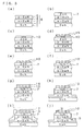
- nitride semiconductor layers 1 to 5 are laminated as shown in Fig. 3(a) .
- the semiconductor lamination portion is formed by a method of metal organic chemical vapor deposition (MOCVD), supplying necessary gasses such as a reactant gas like trimethyl gallium (TMG), ammonia (NH 3 ), trimethyl aluminium (TMA), trimethyl indium (TMIn) or the like, and a dopant gas like SiH 4 for making an n-type, or a dopant gas like cyclopentadienyl magnesium (Cp 2 Mg), dimethyl zinc (DMZn) or the like for making a p-type.
- MOCVD metal organic chemical vapor deposition
- the low temperature buffer layer 2 made of a GaN layer is formed on an insulating substrate 1 made of, for example sapphire, in a thickness of approximately 0.005 to 0.1 ⁇ m, at a low temperature of, for example, approximately 400 to 600 °C, thereafter, the n-type layer (barrier layer) 3 made of n-type GaN is formed in a thickness of approximately 1 to 10 ⁇ m by raising a temperature to a high temperature of approximately 600 to 1200 °C.
- the active layer 4 is formed which has a structure of a multiple quantum well (MQW) formed in a thickness of approximately 0.05 to 0.3 ⁇ m by laminating 3 to 8 pairs of well layers made of, for example, In 0.13 Ga 0.87 N and having a thickness of 1 to 3 nm, and barrier layers made of GaN and having a thickness of 10 to 20 nm.
- MQW multiple quantum well
- the p-type layer 5 made of GaN is laminated 0.2 to 1 ⁇ m thick in total by raising a temperature in a growth furnace to approximately 950 to 1,100 °C.
- a protection film made of SiN or the like is provided on the surface, annealing is carried out at a temperature of approximately 400 to 800 for approximately 10 to 60 min in order to for activate the p-type dopant, and, as shown in Fig. 3(b) , the light transmitting conductive layer 7 is formed with a thickness of approximately 0.7 to 10 ⁇ m by forming the ZnO film by a sputtering method or the like.
- the insulating film 10 is formed with a thickness of approximately 0.1 to 10 ⁇ m, for example, by a SOG method. Then, as shown in Fig.
- a photo resist film is formed on a surface thereof, and a mask 15 is formed by patterning so as to match to the concave-convex pattern by a photolithography method.
- a mask 15 is formed by patterning so as to match to the concave-convex pattern by a photolithography method.
- dry etching such as, for example, a RIE method or the like, the insulating film 10 exposed from the mask 15 is etched, thereafter the mask 15 is removed.
- the light transmitting conductive layer 7 exposed from the insulating film 10 is etched so as to be left with a thickness of approximately 0.05 ⁇ m or more by using the insulating film 10 for a mask and by a ICP etching method using a chlorine group gas.
- a part (surrounding region of a chip and region for forming the n-side electrode) of the semiconductor lamination portion 6 and the light transmitting conductive layer, which are to be etched, is exposed and etched, as shown in Fig. 3(h) , by supplying chlorine gas and silicon tetrachloride gas, and applying a RF power.
- the n-type layer 3 is exposed by etching parts of the semiconductor lamination portion 6, which are exposed not covered by the mask, at a surrounding region of a chip and a region for forming the n-side electrode 9.
- the photo resist film 16 is removed.
- a photo resist film 17 is formed on the entire surface again and an opening is formed at a place for forming the p-side electrode 8. Then, the light transmitting conductive layer 7 is exposed by removing an exposed part of the insulating film 10 by etching, and subsequently, the p-side electrode 8 is formed by forming a Ti film having a thickness of 0.1 ⁇ m and a Au film having a thickness of 0.3 ⁇ m by a lift-off method.
- a Ti film having a thickness of 0.01 ⁇ m and an Al film having a thickness of 0.25 ⁇ m are formed by the lift-off method, and by sintering to make an alloy by applying a heat treatment of approximately 600 °C, the n-side electrode 9 is formed. And, by dividing a wafer into chips, the LED chip having a structure shown in Fig. 2 is formed.
- FIG. 4 A result of measuring luminance of right above in the structure shown in Fig. 2 obtained when a size (diameter) of the concave 7a is varied is shown in Fig. 4 .
- case A conventional structure
- case B having concaves with a diameter d of the concave 7a of 2 ⁇ m and an interval s of the concave 7a of 2 ⁇ m
- case C having concaves with a diameter d of the concave 7a of 5 ⁇ m and an interval s of the concave 7a of 2 ⁇ m
- case D having concaves with a diameter d of the concave 7a of 10 ⁇ m and an interval s of the concave 7a of 4 ⁇ m.
- a thickness of the ZnO film 7 is 0.75 ⁇ m
- an etching depth of the ZnO film 7 is 0.7 ⁇ m
- a thickness of the insulating film 10 is 0.18 ⁇ m. From Fig. 4 , it is understood that the luminance is highest when the diameter is 5 ⁇ m and is rather lowered when the diameter becomes large to approximately 10 ⁇ m. Namely, it is found that the size of the pattern is preferably approximately 3 to 10 ⁇ m.
- the interval s is approximately 1 ⁇ m, since it is a convex, it is not filled by the insulating layer 10, the luminance of the same level as that of a case of 2 ⁇ m can be obtained, and the interval may be approximately 1 to 10 ⁇ m, preferably approximately 3 to 7 ⁇ m.
- the luminance is improved in any size.
- the luminance obtained when the passivation film is formed on the entire surface with a SiN film is measured, and a variation of the luminance caused by the passivation film is within a measurement error and can be hardly observed.
- the concave is low like approximately 2 ⁇ m, the diameter d is also small like approximately 1 ⁇ m, and the concave is filled with the passivation film, improvement of the luminance can be hardly observed.
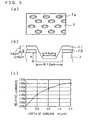
- FIG. 5(c) A simulated result of variation of the luminance due to a depth of the concave and convex is similarly shown in Fig. 5(c) .
- the simulated result is a data obtained in the example in which, as shown in Fig. 5(a) , the diameter of the concave 7a provided in the light transmitting conductive layer 7 is set to approximately 10 ⁇ m, the interval s approximately 4 ⁇ m, and, furthermore, a passivation film 11 is provided on the surface as an enlarged explanatory cross-sectional view of one concave 7a is shown in Fig. 5(b) .
- the thickness of the ZnO film 7 is a constant value of 2.2 ⁇ m and only the depth of the concave 7a is varied. Obviously from Fig. 5(c) , it is understood that the luminance is improved accompanied with increasing of the depth of the concave 7a.
- the concaves and convexes are formed by forming the concaves and the convexes not on the surface of the nitride semiconductor layer but on the surface of the light transmitting conductive layer 7 provided thereon, the concaves and the convexes can be formed on the surface by very easy etching, and, at the same time, since dry etching of hard nitride semiconductor is not necessary, the nitride semiconductor layer such as the p-type layer or the like is prevented from a damage. Therefore, not only a manufacturing process becomes very simple, but also the luminance is significantly improved because no damage to the semiconductor layers occurs.
- the insulating film 10 made of SiO 2 or the like on the light transmitting conductive layer 7 and using it for a mask for patterning the light transmitting conductive layer, a very thick film can be formed very easily because the insulating film can be easily formed by a SOG method or a CVD method.
- the SiO 2 is preferable because light can be more easily taken out from the convexes.
- Fig. 6 is an explanatory cross-sectional view of another embodiment of the present invention.
- the above-described concaves and convexes are preferably formed on a surface of taking out light, however, even in case of flip-chip mounting in which an upper surface side of the semiconductor lamination portion is a mounting side and light is taken out from the substrate side, it is found that the luminance can be improved by forming the concaves and convexes in the light transmitting conductive layer 7.
- a structure, in which the convexes 7a are formed in the light transmitting conductive layer 7, the insulating film 10 is provided on the convexes 7a, and a surface thereof is covered by the passivation film 11, is same as that described above, however, in this embodiment, the surface where the concaves and convexes are formed is not the light taking out surface, and a metal film 12 made of, for example, Ag or Al is provided on the almost entire area of the surface so as to connect to the p-side electrode 8.
- the n-type layer 3 is exposed by etching a part of the semiconductor lamination portion 6 in order to form the n-side electrode 9, however, even in case of a semiconductor substrate such as SiC, similarly by forming the concaves and convexes on the surface of the light transmitting conductive layer 7 provided on the surface of the semiconductor lamination portion 6, the efficiency of taking light out can be improved in the same manner.
- the structure of the semiconductor lamination portion or the like is same as that of the above-described example and the explanation is omitted.
- the light emitting device by the present invention can be used for back lights for liquid crystal display devices or the like, light sources of every kinds, traffic signals or lighting devices for replacing electric lamps or the like, and electronic appliance of every kinds.
Landscapes
- Led Devices (AREA)
- Electrodes Of Semiconductors (AREA)
Claims (7)
- Halbleiterlichtemissionsvorrichtung mit:einem Substrat (1);einem Halbleiterschichtabschnitt (6) aus einem Nitridhalbleiter, der auf einer Oberfläche des Substrates (1) bereitgestellt ist, und der durch Schichten einer n-Schicht (3) und einer p-Schicht (5) unter Ausbildung einer Lichtemissionsschicht ausgebildet ist;einer lichtübertragenden leitenden Schicht (7), die auf einer Oberflächenseite des Halbleiterschichtabschnitts (6) bereitgestellt ist, wobei die lichtübertragende leitende Schicht (7) eine Konkav-Konvex-Struktur aufweist, welche eine Vielzahl von Höhlungen (7a) auf ihrer oberen Oberfläche aufweist, und wobei jede der Höhlungen (7a) so ausgebildet ist, dass ein Teil der lichtübertragenden leitenden Schicht (7) am Grund verbleibt;einer ersten Elektrode (8), die auf der lichtübertragenden leitenden Schicht (7) so bereitgestellt ist, dass sie mit einer Leitfähigkeitsschicht (5) der Oberflächenseite des Halbleiterschichtabschnitts (6) elektrisch verbunden ist; undeiner zweiten Elektrode (9), die so bereitgestellt ist, dass sie mit einer Leitfähigkeitsschicht (3) einer unteren Schichtseite des Halbleiterschichtabschnitts (6) elektrisch verbunden ist,
dadurch gekennzeichnet, dasseine isolierende Schicht (10) mit einem kleineren Brechungsindex als den der lichtübertragenden leitenden Schicht (7) nur auf den Wölbungen der Konkav-Konvex-Struktur bereitgestellt ist, wodurch eine große Stufendifferenz in der Konkav-Konvex-Struktur ausgebildet ist, undeine Passivierungsschicht (11) auf der Oberfläche der Konkav-Konvex-Struktur derart bereitgestellt ist, dass die Höhlungen (7a) nicht mit der Passivierungsschicht gefüllt sind. - Halbleiterlichtemissionsvorrichtung nach Anspruch 1, wobei die lichtübertragende leitende Schicht (7) und die Höhlungen (7a) so ausgebildet sind, dass eine Dicke der lichtübertragenden leitenden Schicht (7), die unter den Höhlungen (7a) verbleibt, 0,05 µm oder mehr beträgt, und eine Tiefe jeder der Höhlungen (7a) 2 bis 10 µm beträgt.
- Halbleiterlichtemissionsvorrichtung nach Anspruch 2, wobei eine Draufsicht jeder der Höhlungen (7a) kreisförmig ist, ein Durchmesser jeder der Höhlungen (7a) 3 bis 10 µm beträgt, und ein minimales Intervall zwischen jedem der Höhlungen (7a) 1 bis 10 µm beträgt.
- Halbleiterlichtemissionsvorrichtung nach einem der Ansprüche 1 bis 3, wobei eine Schichtdicke der Passivierungsschicht (11) auf 1 µm oder weniger eingestellt ist.
- Halbleiterlichtemissionsvorrichtung nach einem der Ansprüche 1 bis 4, wobei eine Metallschicht aus Silber oder Aluminium auf nahezu der gesamten Oberfläche der Konkav-Konvex-Struktur durch eine zwischenliegende Passivierungsisolierungsschicht bereitgestellt ist, und die Halbleiterlichtemissionsvorrichtung so angebracht ist, dass die Lichtausgangsoberfläche die Substratseite ist.
- Verfahren zur Herstellung einer Halbleiterlichtemissionsvorrichtung mit den Schritten:(a) Ausbilden eines Halbleiterschichtabschnitts (6) auf einem Substrat (1) durch Schichten einer n-Schicht (3) und einer p-Schicht (5), sodass eine Lichtemissionsschicht ausgebildet wird;(b) Ausbilden einer lichtübertragenden leitenden Schicht (7) auf einer Oberfläche des Halbleiterschichtabschnitts (6);(c) Ausbilden einer isolierenden Schicht auf der lichtübertragenden leitenden Schicht (7);(d) Ausbilden einer Fotoresistlackschicht auf einer Oberfläche der isolierenden Schicht und Ausbilden eines Musters zum Ausbilden von Höhlungen (7a) und Wölbungen;(e) Strukturieren der isolierenden Schicht unter Verwenden der Fotoresistlackschicht als Maske; und(f) Ausbilden einer Konkav-Konvex-Struktur auf der lichtübertragenden leitenden Schicht (7) durch Ätzen der lichtübertragenden leitenden Schicht (7) unter Verwenden der isolierenden Schicht als Maske, sodass die Konkav-Konvex-Struktur eine Vielzahl von Höhlungen (7a) auf der Oberfläche der lichtübertragenden leitenden Schicht (7) aufweist, wobei jede der Höhlungen (7a) so ausgebildet ist, dass ein Teil der lichtübertragenden leitenden Schicht (7) am Grund verbleibt,dadurch gekennzeichnet, dass
die isolierende Schicht (10) einen kleineren Brechungsindex als den der lichtübertragenden leitenden Schicht (7) aufweist, und nur auf den Wölbungen der Konkav-Konvex-Struktur verbleibt, wodurch eine große Stufendifferenz in der Konkav-Konvex-Struktur ausgebildet wird, und
wobei das Verfahren ferner den Schritt aufweist (g) Ausbilden einer Passivierungsschicht (11) auf der Oberfläche der Konkav-Konvex-Struktur derart, dass die Höhlungen (7a) nicht mit der Passivierungsschicht (11) gefüllt sind. - Verfahren zur Herstellung der Halbleiterlichtemissionsvorrichtung nach Anspruch 6, wobei die isolierende Schicht durch ein Glasaufschleuderungsverfahren ausgebildet wird, und nach Verwendung der isolierenden Schicht als Maske die isolierende Schicht belassen wird, wie sie ist.
Applications Claiming Priority (2)
| Application Number | Priority Date | Filing Date | Title |
|---|---|---|---|
| JP2005380682A JP4954549B2 (ja) | 2005-12-29 | 2005-12-29 | 半導体発光素子およびその製法 |
| PCT/JP2006/326216 WO2007074897A1 (ja) | 2005-12-29 | 2006-12-28 | 半導体発光素子およびその製法 |
Publications (3)
| Publication Number | Publication Date |
|---|---|
| EP1968124A1 EP1968124A1 (de) | 2008-09-10 |
| EP1968124A4 EP1968124A4 (de) | 2009-09-23 |
| EP1968124B1 true EP1968124B1 (de) | 2012-10-10 |
Family
ID=38218119
Family Applications (1)
| Application Number | Title | Priority Date | Filing Date |
|---|---|---|---|
| EP06843594A Not-in-force EP1968124B1 (de) | 2005-12-29 | 2006-12-28 | Halbleiter-leuchtelement und prozess zu seiner herstellung |
Country Status (7)
| Country | Link |
|---|---|
| US (1) | US8304795B2 (de) |
| EP (1) | EP1968124B1 (de) |
| JP (1) | JP4954549B2 (de) |
| KR (1) | KR20080081934A (de) |
| CN (1) | CN101351899B (de) |
| TW (1) | TW200739959A (de) |
| WO (1) | WO2007074897A1 (de) |
Families Citing this family (38)
| Publication number | Priority date | Publication date | Assignee | Title |
|---|---|---|---|---|
| JP2008244425A (ja) * | 2007-02-21 | 2008-10-09 | Mitsubishi Chemicals Corp | GaN系LED素子および発光装置 |
| KR101382677B1 (ko) * | 2007-04-16 | 2014-04-07 | 엘지이노텍 주식회사 | 웨이퍼 기판, 반도체 발광소자 및 웨이퍼 기판을 이용한 반도체 발광소자 제조방법 |
| JP4829190B2 (ja) | 2007-08-22 | 2011-12-07 | 株式会社東芝 | 発光素子 |
| US7847312B2 (en) | 2007-09-14 | 2010-12-07 | Sharp Kabushiki Kaisha | Nitride semiconductor light-emitting device |
| KR101449030B1 (ko) | 2008-04-05 | 2014-10-08 | 엘지이노텍 주식회사 | 그룹 3족 질화물계 반도체 발광다이오드 소자 및 이의 제조방법 |
| KR20090106299A (ko) * | 2008-04-05 | 2009-10-08 | 송준오 | 오믹접촉 광추출 구조층을 구비한 그룹 3족 질화물계반도체 발광다이오드 소자 및 이의 제조 방법 |
| JP5282503B2 (ja) | 2008-09-19 | 2013-09-04 | 日亜化学工業株式会社 | 半導体発光素子 |
| JP5226449B2 (ja) * | 2008-10-03 | 2013-07-03 | スタンレー電気株式会社 | 半導体発光装置 |
| US8183575B2 (en) * | 2009-01-26 | 2012-05-22 | Bridgelux, Inc. | Method and apparatus for providing a patterned electrically conductive and optically transparent or semi-transparent layer over a lighting semiconductor device |
| US8697979B1 (en) * | 2009-05-15 | 2014-04-15 | The United States Of America As Represented By The Secretary Of The Navy | Solar-powered system for generation and storage of hydrogen gas in substrate microstructures |
| JP5434288B2 (ja) * | 2009-06-12 | 2014-03-05 | 豊田合成株式会社 | 半導体発光素子、半導体発光素子の製造方法、半導体発光素子を備えたランプ、照明装置および電子機器 |
| JP2011009382A (ja) * | 2009-06-24 | 2011-01-13 | Rohm Co Ltd | 半導体発光素子 |
| EP2485279B1 (de) * | 2009-09-30 | 2018-08-15 | Kyocera Corporation | Lichtemittierendes element und verfahren zur herstellung des lichtemittierenden elements |
| JP2011187616A (ja) * | 2010-03-08 | 2011-09-22 | Toshiba Corp | 半導体発光素子およびその製造方法 |
| KR101047739B1 (ko) * | 2010-04-28 | 2011-07-07 | 엘지이노텍 주식회사 | 발광소자, 발광소자의 제조방법, 발광소자 패키지 및 조명시스템 |
| EP2387081B1 (de) * | 2010-05-11 | 2015-09-30 | Samsung Electronics Co., Ltd. | Lichtemittierende Halbleitervorrichtung und Verfahren zu ihrer Herstellung |
| KR101165259B1 (ko) * | 2010-07-08 | 2012-08-10 | 포항공과대학교 산학협력단 | MgO피라미드 구조를 갖는 발광소자 및 그 제조방법 |
| CN101908593A (zh) * | 2010-07-15 | 2010-12-08 | 山东华光光电子有限公司 | GaN基LED图形化透明导电薄膜的制作方法 |
| KR101000311B1 (ko) * | 2010-07-27 | 2010-12-13 | (주)더리즈 | 반도체 발광소자 및 그 제조방법 |
| CN102479903A (zh) * | 2010-11-25 | 2012-05-30 | 同方光电科技有限公司 | 一种能增强横向电流扩展的发光二极管 |
| CN102479891A (zh) * | 2010-11-30 | 2012-05-30 | 比亚迪股份有限公司 | 一种发光二极管外延片、芯片及其制作方法 |
| GB2487917B (en) | 2011-02-08 | 2015-03-18 | Seren Photonics Ltd | Semiconductor devices and fabrication methods |
| TWI515936B (zh) * | 2011-12-15 | 2016-01-01 | 友達光電股份有限公司 | 發光裝置及其製作方法 |
| CN103311379B (zh) * | 2012-03-08 | 2016-12-14 | 无锡华润华晶微电子有限公司 | 一种GaN基LED以及制造GaN基LED的方法 |
| JP2014011333A (ja) * | 2012-06-29 | 2014-01-20 | Daiichi Jitsugyo Kk | 光半導体素子およびその製造方法 |
| KR101963227B1 (ko) | 2012-09-28 | 2019-03-28 | 삼성전자주식회사 | 파워 스위칭 소자 및 그 제조방법 |
| US9000414B2 (en) * | 2012-11-16 | 2015-04-07 | Korea Photonics Technology Institute | Light emitting diode having heterogeneous protrusion structures |
| JP6176032B2 (ja) * | 2013-01-30 | 2017-08-09 | 日亜化学工業株式会社 | 半導体発光素子 |
| JP6307703B2 (ja) | 2013-05-31 | 2018-04-11 | パナソニックIpマネジメント株式会社 | 波長変換素子、波長変換素子を備えた発光装置、発光装置を備えた車両、および波長変換素子の製造方法 |
| TW201513397A (zh) * | 2013-09-26 | 2015-04-01 | Lextar Electronics Corp | 發光二極體之製造方法 |
| CN103594592B (zh) * | 2013-11-08 | 2016-06-01 | 溧阳市江大技术转移中心有限公司 | 具有粗化透明电极的倒装发光二极管 |
| KR102142716B1 (ko) * | 2014-03-13 | 2020-08-07 | 엘지이노텍 주식회사 | 발광소자 |
| DE102014107555A1 (de) | 2014-05-28 | 2015-12-03 | Osram Opto Semiconductors Gmbh | Elektrische Kontaktstruktur für ein Halbleiterbauelement und Halbleiterbauelement |
| CN105655460B (zh) * | 2014-12-08 | 2018-09-11 | 比亚迪股份有限公司 | Led芯片及其制备方法 |
| KR102611980B1 (ko) | 2016-12-14 | 2023-12-08 | 삼성전자주식회사 | 멀티 컬러를 구현할 수 있는 발광 소자 |
| JP6608352B2 (ja) * | 2016-12-20 | 2019-11-20 | Dowaエレクトロニクス株式会社 | 半導体発光素子およびその製造方法 |
| KR102111647B1 (ko) * | 2018-07-24 | 2020-05-15 | 주식회사 세미콘라이트 | 반도체 발광소자 |
| JP7134902B2 (ja) * | 2019-03-05 | 2022-09-12 | キオクシア株式会社 | 半導体装置 |
Family Cites Families (12)
| Publication number | Priority date | Publication date | Assignee | Title |
|---|---|---|---|---|
| US5955749A (en) * | 1996-12-02 | 1999-09-21 | Massachusetts Institute Of Technology | Light emitting device utilizing a periodic dielectric structure |
| JP3469484B2 (ja) | 1998-12-24 | 2003-11-25 | 株式会社東芝 | 半導体発光素子およびその製造方法 |
| JP3782357B2 (ja) * | 2002-01-18 | 2006-06-07 | 株式会社東芝 | 半導体発光素子の製造方法 |
| JP4122785B2 (ja) * | 2002-01-30 | 2008-07-23 | 日亜化学工業株式会社 | 発光素子 |
| JP3956918B2 (ja) * | 2002-10-03 | 2007-08-08 | 日亜化学工業株式会社 | 発光ダイオード |
| US7102175B2 (en) * | 2003-04-15 | 2006-09-05 | Matsushita Electric Industrial Co., Ltd. | Semiconductor light-emitting device and method for fabricating the same |
| JP2005005679A (ja) * | 2003-04-15 | 2005-01-06 | Matsushita Electric Ind Co Ltd | 半導体発光素子およびその製造方法 |
| JP2005277374A (ja) * | 2004-02-26 | 2005-10-06 | Toyoda Gosei Co Ltd | Iii族窒化物系化合物半導体発光素子及びその製造方法 |
| TWI244221B (en) * | 2004-03-01 | 2005-11-21 | Epistar Corp | Micro-reflector containing flip-chip light emitting device |
| KR100878433B1 (ko) * | 2005-05-18 | 2009-01-13 | 삼성전기주식회사 | 발광소자의 오믹컨택층 제조방법 및 이를 이용한발광소자의 제조방법 |
| WO2006132013A1 (ja) * | 2005-06-09 | 2006-12-14 | Rohm Co., Ltd | 半導体発光素子 |
| US20070082418A1 (en) * | 2005-10-11 | 2007-04-12 | National Chung-Hsing University | Method for manufacturing a light emitting device and light emitting device made therefrom |
-
2005
- 2005-12-29 JP JP2005380682A patent/JP4954549B2/ja not_active Expired - Fee Related
-
2006
- 2006-12-28 CN CN200680049842XA patent/CN101351899B/zh not_active Expired - Fee Related
- 2006-12-28 KR KR1020087015461A patent/KR20080081934A/ko not_active Withdrawn
- 2006-12-28 US US12/087,173 patent/US8304795B2/en not_active Expired - Fee Related
- 2006-12-28 EP EP06843594A patent/EP1968124B1/de not_active Not-in-force
- 2006-12-28 TW TW095149510A patent/TW200739959A/zh unknown
- 2006-12-28 WO PCT/JP2006/326216 patent/WO2007074897A1/ja not_active Ceased
Also Published As
| Publication number | Publication date |
|---|---|
| CN101351899A (zh) | 2009-01-21 |
| WO2007074897A1 (ja) | 2007-07-05 |
| KR20080081934A (ko) | 2008-09-10 |
| TW200739959A (en) | 2007-10-16 |
| JP2007184313A (ja) | 2007-07-19 |
| CN101351899B (zh) | 2012-01-04 |
| JP4954549B2 (ja) | 2012-06-20 |
| EP1968124A1 (de) | 2008-09-10 |
| US20090026475A1 (en) | 2009-01-29 |
| EP1968124A4 (de) | 2009-09-23 |
| US8304795B2 (en) | 2012-11-06 |
Similar Documents
| Publication | Publication Date | Title |
|---|---|---|
| US8304795B2 (en) | Semiconductor light emitting device with concave-convex pattern and method for manufacturing the same | |
| US8124985B2 (en) | Semiconductor light emitting device and method for manufacturing the same | |
| TWI720026B (zh) | 發光元件 | |
| CN109997234B (zh) | 半导体元件和包括该半导体元件的半导体元件封装 | |
| CN102326270B (zh) | 发光器件 | |
| US12349510B2 (en) | Light-emitting diode, light-emitting diode packaged module and display device including the same | |
| KR20080087135A (ko) | 질화물 반도체 발광 소자 | |
| WO2006132013A1 (ja) | 半導体発光素子 | |
| TW201427082A (zh) | 氮化物半導體發光裝置及其製造方法 | |
| KR20110077707A (ko) | 수직형 발광 다이오드 및 그 제조방법 | |
| CN114725264B (zh) | 半导体器件和包括该半导体器件的半导体器件封装 | |
| KR20100137524A (ko) | 발광 다이오드 구조, 램프 장치 및 발광 다이오드 구조를 형성하는 방법 | |
| KR102575580B1 (ko) | 반도체 소자 | |
| KR20130044909A (ko) | 발광소자 및 그 제조방법 | |
| CN110199398B (zh) | 半导体器件和包括该半导体器件的半导体器件封装 | |
| KR101203138B1 (ko) | 발광소자와 그 제조방법 | |
| JP4751093B2 (ja) | 半導体発光素子 | |
| US20210288219A1 (en) | Semiconductor device | |
| CN205645855U (zh) | 紫外线发光元件 | |
| US20240372039A1 (en) | Contact interconnect structures for light-emitting diode chips and related methods | |
| TWI887590B (zh) | 發光元件 | |
| KR101115538B1 (ko) | 발광소자와 그 제조방법 | |
| KR102260691B1 (ko) | 발광 다이오드 및 이의 제조 방법 | |
| WO2026015346A1 (en) | Lumiphoric material structures within light-emitting diodes and related methods | |
| WO2023250255A1 (en) | Light extraction structures for light-emitting diode chips and related methods |
Legal Events
| Date | Code | Title | Description |
|---|---|---|---|
| PUAI | Public reference made under article 153(3) epc to a published international application that has entered the european phase |
Free format text: ORIGINAL CODE: 0009012 |
|
| 17P | Request for examination filed |
Effective date: 20080626 |
|
| AK | Designated contracting states |
Kind code of ref document: A1 Designated state(s): DE FR GB |
|
| RBV | Designated contracting states (corrected) |
Designated state(s): DE FR GB |
|
| A4 | Supplementary search report drawn up and despatched |
Effective date: 20090826 |
|
| RIC1 | Information provided on ipc code assigned before grant |
Ipc: H01L 33/00 20060101AFI20070822BHEP |
|
| 17Q | First examination report despatched |
Effective date: 20091218 |
|
| REG | Reference to a national code |
Ref country code: DE Ref legal event code: R079 Ref document number: 602006032450 Country of ref document: DE Free format text: PREVIOUS MAIN CLASS: H01L0033000000 Ipc: H01L0033420000 |
|
| RIC1 | Information provided on ipc code assigned before grant |
Ipc: H01L 33/44 20100101ALN20120208BHEP Ipc: H01L 33/42 20100101AFI20120208BHEP |
|
| RIC1 | Information provided on ipc code assigned before grant |
Ipc: H01L 33/42 20100101AFI20120210BHEP Ipc: H01L 33/44 20100101ALN20120210BHEP |
|
| GRAP | Despatch of communication of intention to grant a patent |
Free format text: ORIGINAL CODE: EPIDOSNIGR1 |
|
| DAX | Request for extension of the european patent (deleted) | ||
| GRAS | Grant fee paid |
Free format text: ORIGINAL CODE: EPIDOSNIGR3 |
|
| GRAA | (expected) grant |
Free format text: ORIGINAL CODE: 0009210 |
|
| AK | Designated contracting states |
Kind code of ref document: B1 Designated state(s): DE FR GB |
|
| REG | Reference to a national code |
Ref country code: GB Ref legal event code: FG4D |
|
| REG | Reference to a national code |
Ref country code: DE Ref legal event code: R096 Ref document number: 602006032450 Country of ref document: DE Effective date: 20121206 |
|
| PLBE | No opposition filed within time limit |
Free format text: ORIGINAL CODE: 0009261 |
|
| STAA | Information on the status of an ep patent application or granted ep patent |
Free format text: STATUS: NO OPPOSITION FILED WITHIN TIME LIMIT |
|
| 26N | No opposition filed |
Effective date: 20130711 |
|
| GBPC | Gb: european patent ceased through non-payment of renewal fee |
Effective date: 20130110 |
|
| REG | Reference to a national code |
Ref country code: FR Ref legal event code: ST Effective date: 20130830 |
|
| REG | Reference to a national code |
Ref country code: DE Ref legal event code: R119 Ref document number: 602006032450 Country of ref document: DE Effective date: 20130702 |
|
| PG25 | Lapsed in a contracting state [announced via postgrant information from national office to epo] |
Ref country code: DE Free format text: LAPSE BECAUSE OF NON-PAYMENT OF DUE FEES Effective date: 20130702 |
|
| PG25 | Lapsed in a contracting state [announced via postgrant information from national office to epo] |
Ref country code: FR Free format text: LAPSE BECAUSE OF NON-PAYMENT OF DUE FEES Effective date: 20130102 Ref country code: GB Free format text: LAPSE BECAUSE OF NON-PAYMENT OF DUE FEES Effective date: 20130110 |