EP1844940B1 - Image forming apparatus, optical scanning apparatus, and auto light power control method - Google Patents
Image forming apparatus, optical scanning apparatus, and auto light power control method Download PDFInfo
- Publication number
- EP1844940B1 EP1844940B1 EP07007263A EP07007263A EP1844940B1 EP 1844940 B1 EP1844940 B1 EP 1844940B1 EP 07007263 A EP07007263 A EP 07007263A EP 07007263 A EP07007263 A EP 07007263A EP 1844940 B1 EP1844940 B1 EP 1844940B1
- Authority
- EP
- European Patent Office
- Prior art keywords
- light
- emitting portions
- image
- image period
- period
- Prior art date
- Legal status (The legal status is an assumption and is not a legal conclusion. Google has not performed a legal analysis and makes no representation as to the accuracy of the status listed.)
- Not-in-force
Links
- 230000003287 optical effect Effects 0.000 title claims description 27
- 238000000034 method Methods 0.000 title claims description 13
- 230000015572 biosynthetic process Effects 0.000 claims description 15
- 238000001514 detection method Methods 0.000 claims description 14
- 238000005259 measurement Methods 0.000 claims 1
- 239000004065 semiconductor Substances 0.000 description 18
- 238000012937 correction Methods 0.000 description 4
- 230000007246 mechanism Effects 0.000 description 4
- 230000002349 favourable effect Effects 0.000 description 2
- 239000000463 material Substances 0.000 description 2
- 238000012545 processing Methods 0.000 description 2
- 230000001133 acceleration Effects 0.000 description 1
- PFOLLRNADZZWEX-FFGRCDKISA-N bacampicillin Chemical compound C1([C@@H](N)C(=O)N[C@H]2[C@@H]3N(C2=O)[C@H](C(S3)(C)C)C(=O)OC(C)OC(=O)OCC)=CC=CC=C1 PFOLLRNADZZWEX-FFGRCDKISA-N 0.000 description 1
- 230000008859 change Effects 0.000 description 1
- 230000007423 decrease Effects 0.000 description 1
- 230000003247 decreasing effect Effects 0.000 description 1
- 230000007613 environmental effect Effects 0.000 description 1
- 230000006870 function Effects 0.000 description 1
- 230000007274 generation of a signal involved in cell-cell signaling Effects 0.000 description 1
- 238000012986 modification Methods 0.000 description 1
- 230000004048 modification Effects 0.000 description 1
- 230000002093 peripheral effect Effects 0.000 description 1
- 230000008569 process Effects 0.000 description 1
- 230000004043 responsiveness Effects 0.000 description 1
- 238000012546 transfer Methods 0.000 description 1
- 239000002699 waste material Substances 0.000 description 1
Images


Classifications
-
- H—ELECTRICITY
- H04—ELECTRIC COMMUNICATION TECHNIQUE
- H04N—PICTORIAL COMMUNICATION, e.g. TELEVISION
- H04N1/00—Scanning, transmission or reproduction of documents or the like, e.g. facsimile transmission; Details thereof
- H04N1/04—Scanning arrangements, i.e. arrangements for the displacement of active reading or reproducing elements relative to the original or reproducing medium, or vice versa
- H04N1/113—Scanning arrangements, i.e. arrangements for the displacement of active reading or reproducing elements relative to the original or reproducing medium, or vice versa using oscillating or rotating mirrors
- H04N1/1135—Scanning arrangements, i.e. arrangements for the displacement of active reading or reproducing elements relative to the original or reproducing medium, or vice versa using oscillating or rotating mirrors for the main-scan only
-
- H—ELECTRICITY
- H04—ELECTRIC COMMUNICATION TECHNIQUE
- H04N—PICTORIAL COMMUNICATION, e.g. TELEVISION
- H04N1/00—Scanning, transmission or reproduction of documents or the like, e.g. facsimile transmission; Details thereof
- H04N1/04—Scanning arrangements, i.e. arrangements for the displacement of active reading or reproducing elements relative to the original or reproducing medium, or vice versa
- H04N1/047—Detection, control or error compensation of scanning velocity or position
- H04N1/053—Detection, control or error compensation of scanning velocity or position in main scanning direction, e.g. synchronisation of line start or picture elements in a line
-
- H—ELECTRICITY
- H04—ELECTRIC COMMUNICATION TECHNIQUE
- H04N—PICTORIAL COMMUNICATION, e.g. TELEVISION
- H04N2201/00—Indexing scheme relating to scanning, transmission or reproduction of documents or the like, and to details thereof
- H04N2201/04—Scanning arrangements
- H04N2201/047—Detection, control or error compensation of scanning velocity or position
- H04N2201/04753—Control or error compensation of scanning position or velocity
- H04N2201/04758—Control or error compensation of scanning position or velocity by controlling the position of the scanned image area
- H04N2201/0476—Control or error compensation of scanning position or velocity by controlling the position of the scanned image area using an optical, electro-optical or acousto-optical element
- H04N2201/04762—Control or error compensation of scanning position or velocity by controlling the position of the scanned image area using an optical, electro-optical or acousto-optical element using a reflecting element
-
- H—ELECTRICITY
- H04—ELECTRIC COMMUNICATION TECHNIQUE
- H04N—PICTORIAL COMMUNICATION, e.g. TELEVISION
- H04N2201/00—Indexing scheme relating to scanning, transmission or reproduction of documents or the like, and to details thereof
- H04N2201/04—Scanning arrangements
- H04N2201/047—Detection, control or error compensation of scanning velocity or position
- H04N2201/04753—Control or error compensation of scanning position or velocity
- H04N2201/04791—Control or error compensation of scanning position or velocity in the sub-scan direction
Definitions
- the present invention relates to an image forming apparatus that performs light exposure using a light source that has a plurality of light-emitting portions.
- APC auto power control
- a multi-beam optical system is also known.
- the system can form a plurality of lines with one scan by using a plurality of light sources.
- a method has been proposed that performs light power control of each light source in a multi-beam optical system by causing all the light sources provided in the multi-beam optical system to emit light in a sequential order in a non-image period within one scanning cycle ( Japanese Patent Application Laid-open No. 7-12709 ).
- a method has also been proposed that feeds a bias current of a level that does not emit light to a laser in order to improve the responsiveness of the laser ( Japanese Patent No. 3255295 ). In order to decide this bias current, light power control is required for each light source.
- US 6 483 529 B discloses a multi-beam scanner which performs APC on each of a plurality of beam emitting points one by one during corresponding time duration; respectively, in a non-image forming area.
- US 5 812 299 discloses a scanning optical device capable of performing tilt correction using a correction member and also performing APC for a light beam of a semiconductor laser.
- US 2004/0008248 A discloses a multi-beam scanning device comprising a monolithic laser array and being capable to perform APC.
- a feature of the present invention is to solve at least one problem among the problems described above and other problems. In this connection, other problems will be understood upon reading through this entire specification.
- the present invention is realized, for example, by the optical scanning apparatus as specified in claims 1 to 8.
- the present invention is realized, for example, by the auto light power control method of an image forming apparatus as specified in claim 9.
- the present invention is realized, for example, by the image forming apparatus as specified in claim 10.
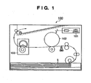
- FIG. 1 is a schematic cross section of an image forming apparatus according to the embodiments
- FIG. 2 is a view which illustrates one example of an exposure apparatus according to the embodiments
- FIG. 3 is a view which illustrates the irradiated positions (spot positions) of laser lights in a case where there is no plane tilt, and the irradiated positions of laser lights in a case where there is a plane tilt;
- FIG. 4 is a view which illustrates one example of a semiconductor laser according to the embodiments.
- FIG. 5 is a view which illustrates the relation between spots and each light-emitting portion of a semiconductor laser according to the embodiments;
- FIG. 6 is a view for describing a control mechanism according to the embodiments.
- FIG. 7 is a view which illustrates one example of an APC unit according to the embodiments.
- FIG. 8 is a basic APC timing chart
- FIG. 9 is an exemplary APC timing chart according to the embodiments.
- FIG. 10 is a flowchart which illustrates an example of an auto light power control method according to the embodiments.
- FIG. 11 is another exemplary APC timing chart according to the embodiments.
- FIG. 12 is a flowchart which illustrates an example of another auto light power control method according to the embodiments.
- FIG. 13 is a flowchart which illustrates APC in a non-image period according to the embodiments.
- FIG. 14 is a view for describing another control mechanism according to the embodiments.
- FIG. 15 is another exemplary APC timing chart according to the embodiments.
- FIG. 16 is another exemplary APC timing chart according to the embodiments.
- FIG. 1 is a schematic cross section of an image forming apparatus according to the embodiments.
- An image forming apparatus 100 is an apparatus which forms monocolor or multi color images.
- the image forming apparatus 100 is implemented as a printing apparatus, an image outputting apparatus, a printer, a copier, a multifunction peripheral or a facsimile machine.
- An optical scanning apparatus (exposure apparatus) 101 is an apparatus which scans a light beam onto a uniformly charged and drum-like photosensitive member 102. Thereby, an electrostatic latent image corresponding to an image signal is formed on the photosensitive member 102.
- the electrostatic latent image is converted into a developer (for example, toner) image by a developing apparatus.
- a fixing apparatus 103 fixes the developer image to a recording medium S onto which the developer image was transferred from the photosensitive member 102.
- the recording medium S may also be referred to as a paper, a sheet, a transfer material, printing material, printing medium or the like.
- FIG. 2 is a view which illustrates one example of the optical scanning apparatus according to this embodiment.
- the optical scanning apparatus 101 has a laser unit 200, a rotating polygonal mirror 210, a polygonal motor 211, an f ⁇ lens 212, a returning mirror 213, a reflecting mirror 214 and a beam detecting sensor 215.
- the optical scanning apparatus 101 also has a half mirror 216 and a light receiving device 217 for detecting the light power of a beam.
- the light receiving device 217 is, for example, a sensor such as a photodiode.
- the laser unit 200 has a laser drive unit 201, a semiconductor laser 202 and a collimator lens 203.
- the semiconductor laser 202 is a light source package that emits laser light when it is driven by the laser drive unit 201.
- the laser light may also be referred to as a "beam”.
- the collimator lens 203 is an optical component which converts a laser light that is emitted from the semiconductor laser 202 into a predetermined beam diameter.
- the laser drive unit 201 is controlled by a main body controller 220.
- the main body controller 220 includes a CPU, a ROM and a RAM, and executes various controls relating to the image forming process.
- the polygonal mirror 210 is a rotating polygonal mirror which deflects a laser light of a predetermined beam diameter while rotating.
- the polygonal mirror 210 comprises a plurality of mirror planes (these may also be referred to as “scanning mirror planes” or “reflecting planes”).
- the polygonal motor 211 is a motor for rotating the polygonal mirror 210.
- the f ⁇ lens 212 is an optical component for focusing a laser light that is reflected by the polygonal mirror 210.
- the returning mirror 213 is an optical component for guiding a laser light that passes through the f ⁇ lens 212 onto the plane of the photosensitive member 102.
- the reflecting mirror 214 is an optical component for guiding a laser light to the beam detecting sensor 215.
- the beam detecting (BD) sensor 215 detects a laser light that is reflected by the reflecting mirror 214, and outputs a beam detection signal (BD signal) to the main body controller 220.
- a beam detection signal is output for each line in the main scanning direction.
- the main body controller 220 detects a cycle in which a beam detection signal is output, and controls the rotation of the polygonal mirror by outputting acceleration signals or deceleration signals to the polygonal motor 211 so that that cycle becomes a predetermined cycle.
- the polygonal motor 211 drives the polygonal mirror 210 based on the control of the main body controller 220.
- APC Auto light power control
- FIG. 3 is a view which illustrates irradiated positions (spot positions) of laser lights in a case where there is no plane tilt, and irradiated positions of laser lights in a case where there is a plane tilt.
- a plane tilt is an inclination in the mirror plane with respect to the rotational axis of the polygonal mirror. More specifically, the term “plane tilt” refers to a state in which a line of intersection between a certain mirror plane and a plane including the rotational axis is not parallel to the rotational axis. The plane tilt may be called “plane tilt shit" or "plane tilt error".
- the polygonal mirror has six mirror planes (A to F). Each straight line in the figure represents the ideal irradiated position of each mirror plane. As will be understood from the figure, at ideal laser irradiated positions of the polygonal mirror at which a plane tilt does not exist or at which a plane tilt can be ignored, the intervals between lines that are formed by each mirror plane are constant.
- the intervals between lines (scanning lines) that are formed by each mirror plane are not constant.
- the mirror plane A and the mirror plane E are not plane-tilted with respect to the rotational axis of the polygonal mirror, it is found that the other mirror planes all incline away from the rotational axis.
- the interval (subscanning pitch interval) between each line in the subscanning direction will not be uniform.
- it is necessary to reduce the pitch nonuniformity by selecting a light-emitting portion(s) that is suitable for the current mirror plane that is to be used to deflect a beam from the light source from among the plurality of mirror planes.
- FIG. 4 is a view which illustrates one example of a semiconductor laser according to this embodiment.
- the semiconductor laser 202 according to the present embodiment has a plurality of light-emitting portions LD1 to LD10. Naturally, each light-emitting portion is also a light source and a single laser device. The respective beams emitted from the plurality of light-emitting portions form respective spots on the photosensitive member 102. According to the present embodiment, the light-emitting portions are disposed in the semiconductor laser 202 such that an interval "d" between the spots of the light-emitting portions is narrower than the resolution in the subscanning direction of the image forming apparatus 100.
- two lines are formed by two light-emitting portions to accelerate the image forming speed.
- LD1 and LD2 constitute a pair to form two adjoining lines.
- LD3 and LD4 constitute a pair
- LD5 and LD6 constitute a pair
- LD7 and LD8 constitute a pair
- LD9 and LD10 constitute a pair.
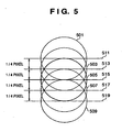
- FIG. 5 is a view which illustrates the relation between spots and each light-emitting portion of the semiconductor laser according to this embodiment.
- Spots 501 to 509 correspond to the light-emitting portions LD1 to LD9, respectively.
- straight lines 511 to 519 represent lines that are formed by the light-emitting portions LD1 to LD9, respectively.
- the intervals "d" between each spot are 1/4 of a pixel, respectively. It is therefore possible according to the present embodiment to reduce the amount of plane tilt according to the following range: +1/2 pixel, +1/4 pixel, -1/4 pixel and -1/2 pixel.
- the laser drive unit 201 causes the light-emitting portions LD1 and LD2 to emit laser lights. If the amount of plane tilt of the mirror plane B is +1/4 pixel, the amount of plane tilt can be reduced if the laser drive unit 201 causes laser lights to be emitted from the light-emitting portions LD7 and LD8. The amount of plane tilt can also be reduced for the other mirror planes by using favorable pairs of light-emitting portions in a similar manner.
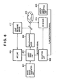
- FIG. 6 is a view for describing a control mechanism according to this embodiment.
- An image signal generation unit 601 is included in the main body controller 220, and generates an image signal that corresponds to image data.
- a selection unit 602 selects light-emitting portions which it is preferable to cause to emit light, respectively, at each timing in a scanning cycle.
- the selection unit 602 selects a specific light-emitting portion (light-emitting portion for BD) for determining the timing as the starting point of image formation in a BD period which is located at the initial stage of a scanning cycle.
- a single scanning cycle includes a BD period, an image period, a non-image period, an OFF period and the like.
- the BD period and the OFF period may also be considered as parts of the non-image period.
- the selection unit 602 selects one or more light-emitting portions that are suitable for each mirror plane in the image period.
- light-emitting portions to be used in an image period are light-emitting portions for which APC is executed in a preceding non-image period.
- a preceding non-image period is preferably the immediately preceding light emitting period.
- the selection unit 602 selects the light-emitting portions to be used in the subsequent image period.
- a mirror plane specifying unit 603 specifies the current mirror plane. More specifically, the mirror plane specifying unit 603 is adapted to output identification information (for example, a plane identification signal) that differs for each mirror plane. For example, a magnet is attached to the lower part of one mirror plane (for example, mirror plane A) and a Hall device is also attached at a position which is on the lower part of the polygonal mirror 210 and which corresponds to the mirror plane at which a laser light will be irradiated. More specifically, a detection signal is output from the Hall device only when the mirror plane A reflects a laser light. Since the relative positional relationship between the mirror plane A and the other mirror planes is fixed, as long as it can detect just the mirror plane A, the mirror plane specifying unit 603 can specify the current mirror plane in accordance with the rotational cycle of the polygonal mirror 210.
- identification information for example, a plane identification signal
- the selection unit 602 selects a light-emitting portion(s) to be used in an image period in accordance with this plane identification signal and outputs a selection signal for driving the selected light-emitting portion(s) to the laser drive unit 201.
- the selection unit 602 may read out the plane identification signal and use it as an address to read out the corresponding selection signal from a memory.
- the relation (table) between the plane identification signals and the selection signals is, for example, set at the time of factory shipment. More specifically, at the factory that manufactures the image forming apparatus 100, the amount of plane tilt of each mirror plane of the polygonal mirror 210 is measured, and selection signals (light-emitting portions) that are effective for reducing the measured amount of plane tilt are determined. That is, light-emitting portions are determined that are suitable for decreasing position errors of spots that are attributable to the amount of plane tilt of the mirror plane. The correlation between each plane identification signal and each selection signal is then stored in the memory.
- the APC unit 604 is a control unit that executes auto light power control for each light-emitting portion in accordance with the light power of beams that are detected by the light receiving device 217.
- the auto light power control comprises a first auto light power control for setting the light power of a beam that is emitted from a light-emitting portion to the target light power, and a second auto light power control for determining the bias current for the light-emitting portion.
- FIG. 7 is a view which illustrates one example of an APC unit according to this embodiment.
- An amplifier 701 is a device for amplifying a detection signal that is output from the light receiving device 217. Naturally, the size of the detection signal correlates to the light power.
- a sample-and-hold circuit 702 is a circuit that samples and holds an amplified detection signal.
- An A/D converter 703 is a circuit that converts the value of a detection signal that is output from the sample-and-hold circuit 702 into a digital signal.
- a light source control circuit 704 controls the value of current flowing to the laser drive unit 201 based on whether or not the value of a detection signal (light power) is a target value. For example, for each light-emitting portion, the light source control circuit 704 may store the value of the bias current and the value of the drive current at the time of image formation in the memory. In this case, the light source control circuit 704 reads out a favorable current value in accordance with a selection signal to set the laser drive unit 201.
- a D/A converter 705 is a circuit which converts a current value that is output from the light source control circuit 704 into an analog value.
- FIG. 8 is a basic APC timing chart. Hereunder, to facilitate the description, a case is described in which a light-emitting portion for BD is subjected to APC in a BD period.
- the light source- control circuit 704 executes APC until the light power of the semiconductor laser 202 reaches a target value. According to FIG. 8 , the light source control circuit 704 increases the drive current by two steps in the first scanning cycle. In this case, since the light power exceeds the target value, the light source control circuit 704 lowers the drive current by one step in the second scanning cycle. In this manner, the light power of each light-emitting portion is maintained at the target value.
- the light source control circuit 704 increases the drive current one step at a time, and when the light power is detected, it decreases the drive current by only one step. Thereby, the bias current is determined.
- FIG. 9 is an exemplary APC timing chart according to this embodiment.
- a period that is described as "LD1 APC” is a period in which APC is executed for the light-emitting portion LD1.
- a period described as “OFF” is a period in which all of the light-emitting portions are switched off.
- a period described as "LD1, 2 DATA” is a period in which the light-emitting portion LD1 and the light-emitting portion LD2 are caused to emit light in accordance with an image signal.
- the light-emitting portions LD9 and LD10 are used for the mirror plane A.
- the respective light powers of the light-emitting portions LD9 and LD10 that are used for image formation directly influence the density of the image. Therefore, these light powers must be precisely adjusted to a predetermined light power. Further, the relation between the drive current and the light power adjusted by APC varies over time due to the influence of heat and the like. It is thus preferable to adjust the light power of each light-emitting portion immediately prior to image formation. More specifically, when performing image formation with the mirror plane A, APC is executed for the light-emitting portions LD9 and LD10 in the immediately preceding non-image period.
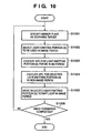
- FIG. 10 is a flowchart which illustrates an example of an auto light power control method according to this embodiment.
- the selection unit 602 specifies a mirror plane as the scanning target using a plane identification signal that is output from the mirror plane specifying unit 603.
- step S1002 the selection unit 602 selects one or more light-emitting portions that are suitable for scanning the specified mirror plane. Naturally, the light-emitting portions are selected on the premise that they will be used in an image period.
- step S1003 the selection unit 602 outputs a selection signal for causing a light-emitting portion for BD (for example, LD1) to light up in a BD period to the laser drive unit 201.
- the laser drive unit 201 drives the light-emitting portion for BD (for example, LD1) in the BD period to emit a beam.
- the APC unit 604 executes APC for the light-emitting portion for BD in the BD period.
- step S1004 the selection unit 602 outputs selection signals for light-emitting portions to be used in the image period to the laser drive unit 201.
- the laser drive unit 201 drives the selected light-emitting portions to emit beams in a non-image period positioned immediately before the image period.
- the APC unit 604 executes APC for each light-emitting portion that emits a light in the non-image period.
- step S1005 the selection unit 602 outputs selection signals for light-emitting portions to be used in the image period to the laser drive unit 201.
- the laser drive unit 201 drives the selected light-emitting portions to emit beams in the image period.
- step S1006 the main body controller 220 determines whether or not image formation is completed. When all images have been formed, it ends the present processing. When the processing is not to be ended, the operation returns to step S1001 to execute scanning for the next mirror plane.
- auto light power control is executed only for light-emitting portions to be used in the next image period.
- the number of light-emitting portions for which auto light power control is executed in a non-image period can be reduced. More specifically, it is possible to relatively extend the control time that can be used per light-emitting portion. It is thus possible to execute auto light power control relatively accurately. As a result, an image with a high degree of stability in regard to density can be provided.
- the influence of a plane tilt can be reduced by specifying a mirror plane on which to scan a beam, and selecting one or more light-emitting portions that are suitable for reducing the influence of a plane tilt of the specified mirror plane.
- the APC unit 604 executes auto light power control for the plurality of light-emitting portions in the above described non-image period.
- the selection unit 602 outputs the selection signals of the light-emitting portions that are the control objects in sequential order. Thereby, APC can be executed for all light-emitting portions to be used in a single image period.
- a non-image period exists before and after an image period in a scanning cycle. Further, in some cases the length of these non-image periods is different. Therefore, executing APC using a longer non-image period can be expected to improve accuracy. However, when using a non-image period that is positioned after the image period, it is necessary to execute APC for light-emitting portions to be used in an image period of the subsequent scanning cycle.
- a method is described in which, for one or more light-emitting portions to be used in an image period belonging to a subsequent scanning cycle, auto light power control is executed in a non-image period that belongs to the preceding scanning cycle.
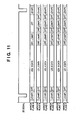
- FIG. 11 is another exemplary APC timing chart according to the embodiments.
- a description is given that focuses on the mirror plane C.
- the mirror plane C the light-emitting portions LD3 and LD4 are used in the image period.
- APC is executed for the light-emitting portions LD3 and LD4 in a non-image period of the immediately preceding mirror plane B.
- APC is executed in a similar manner for the other mirror planes.
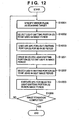
- FIG. 12 is a flowchart which illustrates an example of another auto light power control method according to the embodiments. Steps that were described already are denoted by the same reference numbers and a description thereof is omitted. Upon executing the above described steps S1001 to S1003, the operation proceeds to step S1201.
- step S1201 the selection unit 602 outputs selection signals for light-emitting portions to be used in the image period to the laser drive unit 201.
- the laser drive unit 201 drives the light-emitting portions that are selected for the image period to cause them to emit beams.
- the selection unit 602 selects light-emitting portions to be used in the image period belonging to the next scanning cycle. For example, the selection unit 602 specifies a mirror plane to be used following the current mirror plane from a table stored in the memory, and also selects light-emitting portions to be used for the next mirror plane. Information regarding the order in which the mirror planes are aligned is also stored in the table.
- step S1203 the selection unit 602 outputs the selection signals of the selected light-emitting portions to the laser drive unit 201.
- the laser drive unit 201 drives the selected light-emitting portions to cause them to emit beams in a non-image period.
- the APC unit 604 executes APC for each light-emitting portion that emits light. Thereafter, the operation proceeds to step S1006.
- auto light power control is executed in a non-image period belonging to the preceding scanning cycle.
- APC is executed in non-image periods positioned after the image period.
- a method which skips APC in a non-image period for light-emitting portions for which APC is executed in a BD period.
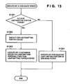
- FIG. 13 is a flowchart which illustrates APC in a non-image period according to this embodiment. This flowchart is one in which the above described step S1004 or S1203 is made into a subroutine.
- step S1301 the selection unit 602 determines whether or not a light-emitting portion for BD is included in the light-emitting portions to be used in the image period. If a light-emitting portion for BD is included, the operation proceeds to step S1302 in which, in order to skip the APC for the light-emitting portion for BD, the selection unit 602 deletes the selection signal of the light-emitting portion for BD from the list of selection signals of light-emitting portions to be used in a non-image period.
- step S1303 the selection unit 602 outputs to the laser drive unit 201 the selection signals for the remaining light-emitting portions, excluding the light-emitting portion for BD, among the selected light-emitting portions.
- the APC unit 604 executes APC for the remaining light-emitting portions.
- step S1304 the operation proceeds to step S1304 to execute the APC as was described in relation to step S1004 or S1203.
- a specific light-emitting portion for example, LD1 to be used in a detection period (BD period) of the image formation timing
- APC is executed in the BD period and the APC in a non-image period is skipped. It is thereby possible to extend the life of the light-emitting portion for BD. Further, since only the necessary minimum number of light-emitting portions are driven in a non-image period, the power consumption is also reduced.
- the light-emitting portion that is not used for image formation constitutes a waste.
- the use frequency of the light-emitting portion for BD will be higher than the other light-emitting portions and the life of the light-emitting portion for BD is liable to expire relatively early.
- the semiconductor laser 202 that has a plurality of light-emitting portions, if the life of even a single light-emitting portion expires, the semiconductor laser 202 must be exchanged.
- the present embodiment by using as a light-emitting portion for BD a light-emitting portion whose use frequency is relatively low, it is possible to extend the exchange cycle of the semiconductor laser.
- the present embodiment is useful for a case in which light-emitting portions to be used with respect to each mirror plane change dynamically.
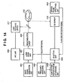
- FIG. 14 is a view for describing another control mechanism according to this embodiment. Parts that were described already are denoted by the same reference numbers and a description thereof is omitted.
- a use frequency measuring unit 1401 measures the use frequency of each light-emitting portion. For example, the use frequency measuring unit 1401 identifies selection signals that are output from the selection unit 602 and counts the number of times each selection signal is output.
- a light-emitting portion for BD determining unit 1402 compares the use frequency of each light-emitting portion to determine the light-emitting portion with the lowest use frequency.
- the selection signal of the thus-determined light-emitting portion is notified to the selection unit 602.
- the selection unit 602 When the scanning cycle enters a BD period, the selection unit 602 outputs the selection signal of the light-emitting portion that is determined.
- FIG. 15 is another exemplary APC timing chart according to this embodiment.
- the light-emitting portions LD3 and LD4 among the light-emitting portions LD1 to LD10 are not used for image formation due to the relation with respect to the amount of plane tilt. More specifically, the use frequency of the light-emitting portions LD3 and LD4 becomes a relatively low value. Therefore the light-emitting portion LD3 is used in a BD period. Naturally the light-emitting portion LD4 may also be used in a BD period.
- FIG. 16 is another exemplary APC timing chart according to this embodiment. This example illustrates an APC timing chart for a case in which APC for light power adjustment and APC for adjusting the bias current are performed.
- Reference numerals LD1APC to LD10APC in FIG. 16 denote APC periods in which APC for adjusting the light power of LD1 to LD10, respectively, is executed. Further, reference numerals LD1BAPC to LD10BAPC denote APC (BAPC) periods for adjusting the bias current of LD1 to LD10, respectively.
- APC APC
- light-emitting portions LD9 and LD10 are used for the mirror plane A.
- the lighting speed of the light-emitting portions LD9 and LD10 that are used for image formation directly influences the quality level of the image. Therefore, these light-emitting portions must be precisely adjusted to a predetermined bias current. Further, the relation between drive current and light power that is adjusted by bias APC varies over time due to the influence of heat and the like. It is therefore preferable for bias current adjustment of each light-emitting portion to be performed directly prior to image formation. More specifically, when forming an image using the mirror plane A, bias APC and light power APC for the light-emitting portions LD9 and LD10 are executed in the immediately preceding non-image period.
- the present invention it is possible to accurately execute auto light power control by reducing the number of light-emitting portions for which auto light power control is executed in a non-image period. It is thus possible to supply an image that has high stability with respect to density.
Landscapes
- Engineering & Computer Science (AREA)
- Multimedia (AREA)
- Signal Processing (AREA)
- Facsimile Scanning Arrangements (AREA)
- Mechanical Optical Scanning Systems (AREA)
- Laser Beam Printer (AREA)
Applications Claiming Priority (1)
| Application Number | Priority Date | Filing Date | Title |
|---|---|---|---|
| JP2006110104A JP2007283512A (ja) | 2006-04-12 | 2006-04-12 | 画像形成装置、光学走査装置および自動光量制御方法 |
Publications (3)
| Publication Number | Publication Date |
|---|---|
| EP1844940A2 EP1844940A2 (en) | 2007-10-17 |
| EP1844940A3 EP1844940A3 (en) | 2008-07-02 |
| EP1844940B1 true EP1844940B1 (en) | 2009-12-30 |
Family
ID=38353388
Family Applications (1)
| Application Number | Title | Priority Date | Filing Date |
|---|---|---|---|
| EP07007263A Not-in-force EP1844940B1 (en) | 2006-04-12 | 2007-04-06 | Image forming apparatus, optical scanning apparatus, and auto light power control method |
Country Status (5)
| Country | Link |
|---|---|
| US (1) | US7719559B2 (enExample) |
| EP (1) | EP1844940B1 (enExample) |
| JP (1) | JP2007283512A (enExample) |
| CN (1) | CN101055449B (enExample) |
| DE (1) | DE602007004015D1 (enExample) |
Families Citing this family (16)
| Publication number | Priority date | Publication date | Assignee | Title |
|---|---|---|---|---|
| JP4868923B2 (ja) * | 2006-04-12 | 2012-02-01 | キヤノン株式会社 | 光走査装置および画像形成装置 |
| JP5439825B2 (ja) * | 2008-01-25 | 2014-03-12 | 株式会社リコー | 画像形成装置および画像形成方法 |
| JP2009178860A (ja) * | 2008-01-29 | 2009-08-13 | Kyocera Mita Corp | 光走査装置,画像形成装置及び画像形成方法 |
| JP5338091B2 (ja) * | 2008-03-07 | 2013-11-13 | 株式会社リコー | 光走査装置および画像形成装置 |
| JP5439874B2 (ja) * | 2008-03-18 | 2014-03-12 | 株式会社リコー | 画像形成装置および画像形成方法 |
| JP5550219B2 (ja) * | 2008-08-28 | 2014-07-16 | キヤノン株式会社 | 光走査装置 |
| JP5441543B2 (ja) * | 2009-07-23 | 2014-03-12 | キヤノン株式会社 | 画像形成装置 |
| JP4856223B2 (ja) * | 2009-09-03 | 2012-01-18 | シャープ株式会社 | 画像形成装置に推奨オプション機能を提示する情報処理装置、その情報処理装置と通信可能な画像形成装置およびそれらを備えた画像形成システム |
| JP5765915B2 (ja) * | 2009-12-22 | 2015-08-19 | キヤノン株式会社 | 画像形成装置 |
| JP2012103492A (ja) * | 2010-11-10 | 2012-05-31 | Fuji Xerox Co Ltd | 光走査装置および画像形成装置 |
| JP6091668B2 (ja) * | 2010-12-10 | 2017-03-08 | キヤノン株式会社 | 画像形成装置 |
| JP5885472B2 (ja) * | 2010-12-10 | 2016-03-15 | キヤノン株式会社 | カラー画像形成装置 |
| JP2012194367A (ja) * | 2011-03-16 | 2012-10-11 | Ricoh Co Ltd | 光走査装置及び画像形成装置 |
| JP6378538B2 (ja) * | 2014-05-21 | 2018-08-22 | キヤノン株式会社 | 画像形成装置 |
| JP6335640B2 (ja) * | 2014-05-22 | 2018-05-30 | キヤノン株式会社 | 光走査装置および画像形成装置 |
| JP6681270B2 (ja) * | 2016-05-19 | 2020-04-15 | キヤノン株式会社 | 画像形成装置及び走査装置 |
Family Cites Families (27)
| Publication number | Priority date | Publication date | Assignee | Title |
|---|---|---|---|---|
| US4600837A (en) | 1983-12-01 | 1986-07-15 | International Business Machines Corporation | Optical scanning apparatus with dynamic scan path control |
| JPS6350809A (ja) | 1986-08-21 | 1988-03-03 | Ricoh Co Ltd | 光書き込み装置 |
| JPH0364729A (ja) * | 1989-08-02 | 1991-03-20 | Canon Inc | 走査線ピッチムラを補正した光走査装置 |
| EP0406844A3 (en) | 1989-07-05 | 1992-08-19 | Canon Kabushiki Kaisha | Scanning optical apparatus |
| JPH03255295A (ja) | 1990-03-01 | 1991-11-14 | Sekisui Chem Co Ltd | 止水用継手 |
| JP3229001B2 (ja) | 1991-03-26 | 2001-11-12 | 株式会社東芝 | 走査光学装置 |
| JP3255295B2 (ja) | 1991-10-14 | 2002-02-12 | ブラザー工業株式会社 | 画像露光装置 |
| JP2804701B2 (ja) | 1993-06-24 | 1998-09-30 | 株式会社日立製作所 | ガスタービンコーティング翼の劣化診断方法及びその装置 |
| IL118458A (en) * | 1995-05-30 | 2000-08-31 | Asahi Optical Co Ltd | Light intensity controlling device |
| JPH09159948A (ja) | 1995-12-05 | 1997-06-20 | Konica Corp | 画像形成装置 |
| DE19703692C2 (de) | 1996-01-31 | 2003-08-21 | Pentax Corp | Abtastvorrichtung |
| JP3239072B2 (ja) | 1996-09-03 | 2001-12-17 | 株式会社東芝 | ビーム光走査装置および画像形成装置 |
| JP3772528B2 (ja) * | 1998-05-08 | 2006-05-10 | コニカミノルタビジネステクノロジーズ株式会社 | レーザ走査光学装置及び画像形成装置 |
| JP2001138570A (ja) * | 1999-11-12 | 2001-05-22 | Ricoh Co Ltd | 画像記録装置 |
| US6483529B1 (en) * | 1999-11-26 | 2002-11-19 | Brother Kogyo Kabushiki Kaisha | Multibeam scanner |
| JP2001174728A (ja) * | 1999-12-15 | 2001-06-29 | Fuji Xerox Co Ltd | 光源の点灯制御方法、及び画像形成装置 |
| US6426767B1 (en) * | 2000-12-29 | 2002-07-30 | Toshiba Tec Kabushiki Kaisha | Image forming apparatus for maintaining a constant beam scanning state |
| JP2003191524A (ja) * | 2001-12-27 | 2003-07-09 | Canon Inc | レーザ駆動回路、画像形成装置およびレーザ駆動方法 |
| US7242441B2 (en) * | 2002-06-10 | 2007-07-10 | Seiko Epson Corporation | Method for manufacturing electro-optical device, and electro-optical device and electronic device manufactured with this manufacturing method |
| US6844892B2 (en) | 2002-06-13 | 2005-01-18 | Pentax Corporation | Multi-beam scanning device |
| EP1439070B1 (en) * | 2003-01-20 | 2008-10-29 | Ricoh Company, Ltd. | Multi-beam scanning device and image forming apparatus using the scanning device |
| JP2004223754A (ja) | 2003-01-20 | 2004-08-12 | Canon Inc | 画像形成装置 |
| JP2005161790A (ja) * | 2003-12-05 | 2005-06-23 | Fuji Xerox Co Ltd | 光走査装置の光量制御方法及び画像形成装置 |
| JP4321764B2 (ja) | 2004-02-23 | 2009-08-26 | 株式会社リコー | 光走査装置及び画像形成装置 |
| JP2006035703A (ja) * | 2004-07-28 | 2006-02-09 | Canon Inc | 光走査装置およびそれを用いた画像形成装置 |
| US7936493B2 (en) * | 2005-06-21 | 2011-05-03 | Ricoh Company, Ltd. | Dot position correcting apparatus, optical scanning apparatus, imaging apparatus, and color imaging apparatus |
| US20080018727A1 (en) * | 2006-07-24 | 2008-01-24 | Kabushiki Kaisha Toshiba | Optical beam scanning apparatus, optical beam scanning method, optical beam scanning program, image forming apparatus, image forming method, image forming program |
-
2006
- 2006-04-12 JP JP2006110104A patent/JP2007283512A/ja active Pending
-
2007
- 2007-04-03 US US11/696,175 patent/US7719559B2/en not_active Expired - Fee Related
- 2007-04-06 DE DE602007004015T patent/DE602007004015D1/de active Active
- 2007-04-06 EP EP07007263A patent/EP1844940B1/en not_active Not-in-force
- 2007-04-06 CN CN2007100908204A patent/CN101055449B/zh not_active Expired - Fee Related
Also Published As
| Publication number | Publication date |
|---|---|
| US20070242128A1 (en) | 2007-10-18 |
| EP1844940A2 (en) | 2007-10-17 |
| EP1844940A3 (en) | 2008-07-02 |
| CN101055449A (zh) | 2007-10-17 |
| US7719559B2 (en) | 2010-05-18 |
| JP2007283512A (ja) | 2007-11-01 |
| CN101055449B (zh) | 2011-04-13 |
| DE602007004015D1 (de) | 2010-02-11 |
Similar Documents
| Publication | Publication Date | Title |
|---|---|---|
| EP1844940B1 (en) | Image forming apparatus, optical scanning apparatus, and auto light power control method | |
| EP1844943B1 (en) | Image forming apparatus and control method thereof | |
| EP1821512B1 (en) | Exposure apparatus | |
| US9091955B2 (en) | Image forming apparatus | |
| US9091956B2 (en) | Image forming apparatus for performing exposure a plurality of times | |
| US7057634B2 (en) | Multi-beam scanning device and image forming apparatus using the scanning device | |
| US7852363B2 (en) | Light scanning apparatus, image forming apparatus, and light power control method | |
| JP4792723B2 (ja) | 画像形成装置 | |
| US8520711B2 (en) | Optical device and method for controlling the same | |
| JP2004101656A (ja) | 画像形成装置、光書込装置および光書込装置のapc制御方法 | |
| JP2016150581A (ja) | 画像形成装置 | |
| JP2023122133A (ja) | 画像形成装置 | |
| JP2004341171A (ja) | 画像形成装置 | |
| US7408567B2 (en) | Light beam scanning apparatus and image forming apparatus | |
| JP2000118040A (ja) | 画像形成装置 | |
| JP2001138570A (ja) | 画像記録装置 | |
| JP3384211B2 (ja) | 半導体レーザの光量制御装置 | |
| JP2009145398A (ja) | 光走査装置、光量制御装置、画像形成装置、及び光量制御方法 | |
| JP2022056082A (ja) | 画像形成装置 | |
| JP2010036352A (ja) | 画像形成装置および光走査装置の制御方法 | |
| JP2013001084A (ja) | 露光装置及びその調整方法、並びに画像形成装置 | |
| JPH09214697A (ja) | 画像形成装置及びその制御方法 | |
| JPH08118724A (ja) | 画像形成装置 | |
| JP2006212871A (ja) | 画像形成装置 | |
| JP2004230718A (ja) | 画像形成装置 |
Legal Events
| Date | Code | Title | Description |
|---|---|---|---|
| PUAI | Public reference made under article 153(3) epc to a published international application that has entered the european phase |
Free format text: ORIGINAL CODE: 0009012 |
|
| AK | Designated contracting states |
Kind code of ref document: A2 Designated state(s): AT BE BG CH CY CZ DE DK EE ES FI FR GB GR HU IE IS IT LI LT LU LV MC MT NL PL PT RO SE SI SK TR |
|
| AX | Request for extension of the european patent |
Extension state: AL BA HR MK YU |
|
| PUAL | Search report despatched |
Free format text: ORIGINAL CODE: 0009013 |
|
| AK | Designated contracting states |
Kind code of ref document: A3 Designated state(s): AT BE BG CH CY CZ DE DK EE ES FI FR GB GR HU IE IS IT LI LT LU LV MC MT NL PL PT RO SE SI SK TR |
|
| AX | Request for extension of the european patent |
Extension state: AL BA HR MK RS |
|
| 17P | Request for examination filed |
Effective date: 20090105 |
|
| AKX | Designation fees paid |
Designated state(s): DE FR GB IT |
|
| GRAP | Despatch of communication of intention to grant a patent |
Free format text: ORIGINAL CODE: EPIDOSNIGR1 |
|
| GRAC | Information related to communication of intention to grant a patent modified |
Free format text: ORIGINAL CODE: EPIDOSCIGR1 |
|
| GRAS | Grant fee paid |
Free format text: ORIGINAL CODE: EPIDOSNIGR3 |
|
| GRAA | (expected) grant |
Free format text: ORIGINAL CODE: 0009210 |
|
| AK | Designated contracting states |
Kind code of ref document: B1 Designated state(s): DE FR GB IT |
|
| REG | Reference to a national code |
Ref country code: GB Ref legal event code: FG4D |
|
| REF | Corresponds to: |
Ref document number: 602007004015 Country of ref document: DE Date of ref document: 20100211 Kind code of ref document: P |
|
| PLBE | No opposition filed within time limit |
Free format text: ORIGINAL CODE: 0009261 |
|
| STAA | Information on the status of an ep patent application or granted ep patent |
Free format text: STATUS: NO OPPOSITION FILED WITHIN TIME LIMIT |
|
| 26N | No opposition filed |
Effective date: 20101001 |
|
| PG25 | Lapsed in a contracting state [announced via postgrant information from national office to epo] |
Ref country code: IT Free format text: LAPSE BECAUSE OF NON-PAYMENT OF DUE FEES Effective date: 20100406 |
|
| REG | Reference to a national code |
Ref country code: FR Ref legal event code: PLFP Year of fee payment: 10 |
|
| PGFP | Annual fee paid to national office [announced via postgrant information from national office to epo] |
Ref country code: GB Payment date: 20160427 Year of fee payment: 10 Ref country code: DE Payment date: 20160430 Year of fee payment: 10 |
|
| PGFP | Annual fee paid to national office [announced via postgrant information from national office to epo] |
Ref country code: FR Payment date: 20160426 Year of fee payment: 10 Ref country code: IT Payment date: 20160405 Year of fee payment: 10 |
|
| REG | Reference to a national code |
Ref country code: DE Ref legal event code: R119 Ref document number: 602007004015 Country of ref document: DE |
|
| GBPC | Gb: european patent ceased through non-payment of renewal fee |
Effective date: 20170406 |
|
| REG | Reference to a national code |
Ref country code: FR Ref legal event code: ST Effective date: 20171229 |
|
| PG25 | Lapsed in a contracting state [announced via postgrant information from national office to epo] |
Ref country code: FR Free format text: LAPSE BECAUSE OF NON-PAYMENT OF DUE FEES Effective date: 20170502 Ref country code: DE Free format text: LAPSE BECAUSE OF NON-PAYMENT OF DUE FEES Effective date: 20171103 |
|
| PG25 | Lapsed in a contracting state [announced via postgrant information from national office to epo] |
Ref country code: GB Free format text: LAPSE BECAUSE OF NON-PAYMENT OF DUE FEES Effective date: 20170406 |
|
| PG25 | Lapsed in a contracting state [announced via postgrant information from national office to epo] |
Ref country code: IT Free format text: LAPSE BECAUSE OF NON-PAYMENT OF DUE FEES Effective date: 20170406 |