EP1821175A1 - Anzeigeeinrichtung mit berührungssensor und ansteuerverfahren für die einrichtung - Google Patents
Anzeigeeinrichtung mit berührungssensor und ansteuerverfahren für die einrichtung Download PDFInfo
- Publication number
- EP1821175A1 EP1821175A1 EP05795610A EP05795610A EP1821175A1 EP 1821175 A1 EP1821175 A1 EP 1821175A1 EP 05795610 A EP05795610 A EP 05795610A EP 05795610 A EP05795610 A EP 05795610A EP 1821175 A1 EP1821175 A1 EP 1821175A1
- Authority
- EP
- European Patent Office
- Prior art keywords
- position detection
- voltage
- frequency
- signal
- touch
- Prior art date
- Legal status (The legal status is an assumption and is not a legal conclusion. Google has not performed a legal analysis and makes no representation as to the accuracy of the status listed.)
- Withdrawn
Links
Images


Classifications
-
- G—PHYSICS
- G06—COMPUTING; CALCULATING OR COUNTING
- G06F—ELECTRIC DIGITAL DATA PROCESSING
- G06F3/00—Input arrangements for transferring data to be processed into a form capable of being handled by the computer; Output arrangements for transferring data from processing unit to output unit, e.g. interface arrangements
- G06F3/01—Input arrangements or combined input and output arrangements for interaction between user and computer
- G06F3/03—Arrangements for converting the position or the displacement of a member into a coded form
- G06F3/041—Digitisers, e.g. for touch screens or touch pads, characterised by the transducing means
- G06F3/044—Digitisers, e.g. for touch screens or touch pads, characterised by the transducing means by capacitive means
- G06F3/0443—Digitisers, e.g. for touch screens or touch pads, characterised by the transducing means by capacitive means using a single layer of sensing electrodes
Definitions
- the present invention relates to a touch-sensored display device which is capable of detecting a position on a display surface that is contacted with a pen, a finger, or the like, and a driving method thereof.
- a touch sensor is an input device which performs position detection as to a place where contact with a finger, a pen, or the like is made, and conveys the intent of an operator to an information processing system.
- Known approaches of position detection are a static capacitive coupling approach, a resistive membrane approach, an infrared approach, an ultrasonic approach, an electromagnetic induction/coupling approach, and so on.
- a touch sensor of the static capacitive coupling approach is disclosed in Patent Document 1, for example.
- a touch sensor of the static capacitive coupling approach is constructed so that terminals for position detection are formed in the four corners of a conductive film for position detection, and an AC voltage is applied to the terminals.
- the transparent conductive film for position detection is coupled to the ground (ground plane) in a capacitive manner.
- the touch sensor is to be disposed on the front face (viewer side) of a display panel such as a liquid crystal panel.
- a display panel such as a liquid crystal panel.
- Noise from the display panel includes, for example, an induced voltage that occurs on the transparent conductive film for position detection, which is comprised in the touch sensor, responsive to a common voltage that is applied to a counter electrode, which is comprised in the liquid crystal panel.
- a shield layer is placed between the transparent conductive film for position detection (which is comprised in the touch sensor) and the liquid crystal panel, the shield layer preventing the touch sensor from being unfavorably affected by noise from the liquid crystal panel. Furthermore, the transparent conductive film for position detection of the touch sensor is disposed sufficiently far from the liquid crystal panel, which also suppresses the influence of noise from the liquid crystal panel.
- a display device which comprises a touch sensor of the resistive membrane approach is disclosed in Patent Document 2, for example.
- the timing with which output data is taken from the touch sensor is varied to ensure that noise originating in the liquid crystal panel will not be mixed in the output data.
- a method for avoiding noise ascribable to the display signal a method is also being practiced in which the position detection of a place of contact is performed during a blanking period, in which the display signal is absent.
- Patent Document 3 a display device and a position detection method comprising a touch sensor of the static capacitive coupling approach, which takes advantage of a voltage which is induced in the conductive film for position detection by a voltage that is supplied to the display panel.
- Patent Document 4 discloses a coordinate detection device which, in order to suppress noise influence, sets an AC voltage to be applied to the conductive film for position detection to a frequency between an n th order harmonic and an (n+1) th order harmonic of the induced voltage.
- Patent Document 5 discloses a coordinate input device which, in order to suppress noise influence, sets an AC voltage to be applied to the conductive film for position detection to a period in the neighborhood of 1/n of the period of the induced voltage.
- Patent Document 1 Japanese National Patent Publication No. 56-500230
- Patent Document 2 Japanese Laid-Open Patent Publication No. 9-128146
- Patent Document 3 Japanese Laid-Open Patent Publication No. 2004-21327
- Patent Document 4 Japanese Laid-Open Patent Publication No. 62-037725
- Patent Document 5 Japanese Laid-Open Patent Publication No. 62-165229
- the detection In the case of avoiding noise influences by performing position detection during a blanking period, the detection must be performed during a vertical blanking period because a horizontal blanking period would not provide enough time for performing the processing for noise avoidance.
- the sampling interval In order to perform position detection during a vertical blanking period, the sampling interval would be 16.7 ms in the case where the liquid crystal is driven at 60 Hz, for example. Such an interval would be too slow for the user of the touch sensor to smoothly input a contacted position.
- the touch-sensored display device described in Patent Document 3 has advantages such as a smaller parallax than those of traditional touch-sensored display devices.
- an induced voltage is utilized to replace an AC voltage source for applying an AC voltage to the conductive film for position detection
- the changes in currents during contact with the touch sensor are small relative to the values of the currents which flow when touch is not being made, and it is susceptible to the influence of the state of driving (content of the display screen) of the display panel, so that a sufficient accuracy of position detection may not be obtained.
- the coordinate detection device of Patent Document 4 has a problem in that noise may occur due to interference between the 2 nd order harmonic of the AC voltage which is applied to the conductive film for position detection and the (2n+1) th order harmonic of the induced voltage.
- the coordinate input device of Patent Document 5 has a problem in that noise may occur due to interference between the n th order harmonic of the AC voltage which is applied to the conductive film for position detection and the induced voltage.
- the output voltage value of the position detection circuit will be affected by the irregular fluctuations or variations due to external factors, thus leading to the problems of lowering of the SN ratio of a signal component to be extracted and lowering of the accuracy of position detection.
- the present invention has been made in view of the above points, and a main objective thereof is to provide a display device with a touch panel, of the static capacitive coupling approach, such that the display device has a small parallax and a high accuracy of position detection.
- a touch-sensored display device is characterized by comprising: a display panel including: an active matrix substrate having a plurality of pixel electrodes, a display medium layer, and a counter substrate disposed on a viewer side of the active matrix substrate via the display medium layer, the counter substrate having a counter electrode which opposes the plurality of pixel electrodes; a display panel driving circuit for supplying display signal voltages to the plurality of pixel electrodes, and supplying to the counter electrode a common voltage which undergoes periodic inversion in polarity; a transparent conductive film for position detection, placed so as to oppose the counter electrode via the counter substrate; a plurality of terminals connected to different points on the transparent conductive film for position detection; an AC voltage generation circuit for supplying an AC voltage for position detection to the plurality of terminals; and a position data generation circuit including: a strobe signal generation circuit for generating a strobe signal which is in synchronization with a polarity inversion period of the common voltage, and a plurality
- each of the plurality of noise-cut current signal generation circuits includes: a current detection circuit for detecting a current flowing from one of the plurality of terminals and outputting a current signal; and a noise elimination circuit for eliminating a predetermined portion from the current signal based on the strobe signal.
- the noise elimination circuit eliminates a portion containing a noise which occurs due to a polarity inversion of the common voltage.
- a horizontal synchronizing signal is supplied to the display panel driving circuit; and the strobe signal generation circuit generates the strobe signal based on the horizontal synchronizing signal.
- the strobe signal generation circuit generates a strobe signal containing a pulse which becomes active after the lapse of a predetermined time (Ts1) from a rise or fall of a pulse contained in the horizontal synchronizing signal, and which becomes inactive after the lapse of a predetermined time (Ts2) from a polarity inversion of the common voltage.
- the display panel driving circuit supplies to the display panel a common voltage which undergoes a polarity inversion after the lapse of a predetermined time (Tc) from a rise or fall of the horizontal synchronizing signal; and the strobe signal generation circuit generates a strobe signal containing a pulse which becomes active after the lapse of a predetermined time (Ts1) from the rise or fall of the horizontal synchronizing signal and which becomes inactive after the lapse of a predetermined time (Ts2) from the rise or fall of the horizontal synchronizing signal, where a relationship Ts1 ⁇ Tc ⁇ Ts2 is satisfied.
- a pulse width of the strobe signal is an integer multiple of one period of the AC voltage for position detection.
- the AC voltage for position detection has a frequency which is an integer multiple of that of the horizontal synchronizing signal.
- the AC voltage for position detection has a frequency which is an integer multiple of that of the strobe signal.
- an inverter is further comprised, wherein, a driving frequency of the inverter is a frequency which is an integer multiple or half integer multiple of that of the horizontal synchronizing signal.
- the inverter is a separately-excited inverter, the driving frequency of the inverter being equal to a frequency of the AC voltage for position detection.
- the driving frequency of the inverter is a frequency which is an integer multiple or half integer multiple of that of the strobe signal.
- an A/D converter which is provided commonly for the plurality of noise-cut current signal generation circuits is further comprised, wherein the position data generation circuit generates the position data based on an output signal from the A/D converter.
- a plurality of sample/hold circuits for simultaneously sampling/holding output signals from the plurality of noise-cut current signal generation circuits are further comprised.
- each of the plurality of noise-cut current signal generation circuits has a current detection circuit for detecting a current flowing from one of the plurality of terminals and outputting a current signal, and a noise elimination circuit for eliminating a predetermined portion from the current signal based on the strobe signal; and an independent compensation element is connected to each of the plurality of current detection circuits.
- each of the plurality of current detection circuits has a differential amplifier, one input of the differential amplifier being electrically connected to one of the plurality of terminals, and the other input being electrically connected to the compensation element.
- impedances of the plurality of compensation elements are substantially equal to impedances of stray capacitances that exist when no contact point is formed on the transparent conductive film for position detection.
- a circuit is further comprised for retaining in an analog or digital manner the noise-cut current signal which is output from each of the plurality of noise-cut current signal generation circuits while no contact point is formed.
- a horizontal synchronizing signal is supplied to the display panel driving circuit; and the AC voltage for position detection has a frequency which is n times (where n is an integer) or 1/n times as large as that of the horizontal synchronizing signal, and is in synchronization with the horizontal synchronizing signal.
- a horizontal synchronizing signal is supplied to the display panel driving circuit; and a frequency of the AC voltage for position detection is a frequency between a first frequency which is n times (where n is an integer) or 1/n times as large as that of the horizontal synchronizing signal and a second frequency which is n+1 times or 1/(n+1) times as large as that of the horizontal synchronizing signal.
- the frequency of the AC voltage for position detection is set so as to be a frequency between the first frequency and the second frequency even when the frequency of the AC voltage for position detection is deviated due to an error in a constant of the AC voltage generation circuit.
- the frequency of the AC voltage for position detection is distant by 1 kHz or more from both the first frequency and the second frequency.
- a frequency which is m times (where m is an integer) or 1/m times as large as that of the AC voltage for position detection is substantially equal to a frequency which is M times (where M is an integer) or 1/M times as large as that of the horizontal synchronizing signal.
- a driving method is a driving method for driving a touch-sensored display device which includes: a display panel including an active matrix substrate having a plurality of pixel electrodes, a display medium layer, and a counter substrate disposed on a viewer side of the active matrix substrate via the display medium layer, the counter substrate having a counter electrode which opposes the plurality of pixel electrodes; a display panel driving circuit for supplying display signal voltages to the plurality of pixel electrodes, and supplying to the counter electrode a common voltage which undergoes periodic inversion in polarity; a transparent conductive film for position detection, placed so as to oppose the counter electrode via the counter substrate; a plurality of terminals connected to different points on the transparent conductive film for position detection; an AC voltage generation circuit for supplying an AC voltage for position detection to each of the plurality of terminals; and a plurality of noise-cut current signal generation circuits each being connected to one of the plurality of terminals, wherein the driving method is characterized by comprising: a step of
- the step of generating the plurality of noise-cut current signals comprises: a step of generating a plurality of current signals by detecting a current flowing from each of the plurality of terminals; and a step of eliminating a portion corresponding to the pulse of the strobe signal from each of the plurality of current signals.
- a step of retaining in an analog or digital manner the plurality of noise-cut current signals generated while no contact point is formed on the transparent conductive film for position detection is further comprised.
- a step of, based on the plurality of noise-cut current signals retained in an analog or digital manner, compensating for stray capacitances that exist when no contact point is formed on the transparent conductive film for position detection is further comprised.
- a step of amplifying an amount of change in current due to a contact point being formed on the transparent conductive film for position detection is further comprised.
- a touch-sensored display device comprising: a display panel including: an active matrix substrate having a plurality of pixel electrodes, a display medium layer, and a counter substrate disposed on a viewer side of the active matrix substrate via the display medium layer, the counter substrate having a counter electrode which opposes the plurality of pixel electrodes; a display panel driving circuit for supplying display signal voltages to the plurality of pixel electrodes, and supplying a common voltage to the counter electrode; a transparent conductive film for position detection, placed so as to oppose the counter electrode via the counter substrate; a plurality of terminals connected to different points on the transparent conductive film for position detection; and a position data generation circuit including a plurality of current detection circuits each detecting a current flowing from one of the plurality of terminals and outputting a current signal, the position data generation circuit generating position data of a contact point which is formed directly or indirectly on the transparent conductive film for position detection, the position data being generated based on the current signals, wherein, an independent compensation element is connected
- each of the plurality of current detection circuits has a differential amplifier, one input of the differential amplifier being electrically connected to one of the plurality of terminals, and the other input being electrically connected to the compensation element.
- impedances of the plurality of compensation elements are substantially equal to impedances of stray capacitances that exist when no contact point is formed on the transparent conductive film for position detection.
- an AC voltage generation circuit for supplying an AC voltage for position detection to the plurality of terminals is further comprised.
- a horizontal synchronizing signal is supplied to the display panel driving circuit; and the AC voltage for position detection has a frequency which is an integer multiple of that of the horizontal synchronizing signal.
- an inverter is further comprised, wherein, a driving frequency of the inverter is a frequency which is an integer multiple or half integer multiple of that of the horizontal synchronizing signal.
- the inverter is a separately-excited inverter, the driving frequency of the inverter being equal to a frequency of the AC voltage for position detection.
- an A/D converter is further comprised which is provided commonly for the plurality of current detection circuits, wherein the position data generation circuit generates the position data based on an output signal from the A/D converter.
- a plurality of sample/hold circuits for simultaneously sampling/holding output signals from the plurality of current detection circuits are further comprised.
- a driving method is a driving method for driving a touch-sensored display device which includes: a display panel including an active matrix substrate having a plurality of pixel electrodes, a display medium layer, and a counter substrate disposed on a viewer side of the active matrix substrate via the display medium layer, the counter substrate having a counter electrode which opposes the plurality of pixel electrodes; a display panel driving circuit for supplying display signal voltages to the plurality of pixel electrodes, and supplying a common voltage to the counter electrode; a transparent conductive film for position detection, placed so as to oppose the counter electrode via the counter substrate; a plurality of terminals connected to different points on the transparent conductive film for position detection; and a position data generation circuit including a plurality of current detection circuits each detecting a current flowing from one of the plurality of terminals and outputting a current signal, the position data generation circuit generating position data of a contact point which is formed directly or indirectly on the transparent conductive film for position detection, the position data being generated based
- step (c) is performed before each of the plurality of current detection circuits detects a current flowing from one of the plurality of terminals.
- a step of sampling/holding for a predetermined period the current signals which are respectively output from the plurality of current detection circuits is further comprised.
- a step of amplifying an amount of change in current due to a contact point being formed on the transparent conductive film for position detection is further comprised.
- noises that occur in currents flowing from terminals of a conductive film for position detection, due to a common voltage which is supplied to a counter electrode of a display panel and which undergoes periodic polarity inversions, are eliminated by using a strobe signal.
- the SN ratio is improved, and the accuracy of position detection is improved.
- the circuit structure can be simplified.
- stray capacitances occurring while no contact point is formed on the transparent conductive film for position detection are compensated for by compensation elements, whereby the accuracy of position detection is improved.
- a touch-sensored display device having little parallax can be provided without having to provide a shield layer between the touch sensor and the liquid crystal panel, or place the conductive film for position detection away from the liquid crystal panel surface.
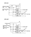
- FIG. 1A and FIG. 1B schematically show the construction of a touch-sensored display device 20 according to one embodiment of the present invention.
- the touch-sensored display device 20 includes a display panel 10 of an active matrix-type (e.g., TFT-type), a transparent conductive film 7 for position detection, a driving circuit 14 for supplying various signals to the display panel 10 , and touch panel circuitry 16 .
- the driving circuit 14 Via a FPC (flexible printed circuit) 13 , the driving circuit 14 is connected to source drivers 12a and gate drivers 12b which are mounted or formed in a monolithic manner on an active matrix substrate 8 of the display panel 10 .
- a position data generation circuit Via an external interface (I/F), predetermined signals such as a video displaying signal are supplied, and a horizontal synchronizing signal H SYC , a vertical synchronizing signal V SYC , a clock signal CLK (pixel clock) and the like are input to the driving circuit 14 .
- the clock signal CLK may be generated within the driving circuit 14 by a PLL circuit, for example.
- a vertical synchronizing signal V SYC , a horizontal synchronizing signal H SYC , and if necessary a clock signal CLK are supplied to the touch panel circuitry 16 .
- a position data generation circuit reference numeral 50 in FIG.
- the touch panel circuitry 16 and an AC voltage generation circuit (reference numeral 18 in FIG. 4 ) (to be described in detail later) are included in the touch panel circuitry 16 , and the display panel driving circuit (reference numeral 40 in FIG. 6 ) includes the driving circuit 14 , the source drivers 12a , and the gate drivers 12b .
- the flows of signals (i.e., interconnection between circuits) in the touch-sensored display device 20 of the present embodiment are exemplary, and can be modified to any logically equivalent interconnection.
- the display panel 10 at least includes: the active matrix substrate 8 having a plurality of pixel electrodes; a display medium layer 4 composed of liquid crystal, for example; and a counter substrate (insulating layer) 6 which is disposed on the viewer side of the display medium layer 4 and on which a transparent counter electrode 5 for driving the display medium layer 4 is formed.
- the transparent conductive film 7 for position detection is placed so as to oppose the transparent counter electrode 5 via the counter substrate 6 of the display panel 10.
- the transparent conductive film 7 for position detection is a transparent conductive film which is formed by a well-known thin-film forming technique such as sputtering, e.g., indium-tin oxide (ITO), indium-zinc oxide (IZO), tin oxide (NESA), or zinc oxide.
- ITO indium-tin oxide
- IZO indium-zinc oxide
- NESA tin oxide
- the sheet resistance value of the transparent conductive film 7 for position detection is preferably 500 to 2000 ⁇ / ⁇ , and more preferably 800 to 1200 ⁇ / ⁇ .
- the film thickness of the transparent conductive film 7 for position detection is preferably 10 to 20 nm.
- the material and film formation method of the transparent conductive film 7 for position detection there is no particular limitation as to the material and film formation method of the transparent conductive film 7 for position detection, and any known material or film formation method may be used. However, in order to obtain a transparent conductive film having good thermal resistance and durability, it is preferable to perform the film formation by sputtering technique using a target which contains Mg.
- the transparent conductive film 7 for position detection may be formed on the surface of a separate touch sensor substrate (not shown) which is composed of glass or transparent plastic, and may be directly adhered by using an adhesive or the like, or mounted via a gap (air layer), to the outer surface (viewer side surface) of the display panel 10.
- the transparent conductive film 7 for position detection may be allowed to face the display panel 10, or conversely, the touch sensor substrate may be allowed to face the display panel 10.
- the display panel and the touch sensor portion are separately produced and combined at last, this being advantageous in terms of production yield and production efficiency.
- the touch sensor substrate is directly adhered to the display panel 10, an interface with air is not formed between the two, thus reducing the reflection of external light (which would hinder displaying).
- the touch sensor substrate is mounted on the outer surface of the display panel 10 with a gap, the displayed image is prevented from becoming disordered due to a pressing (associated with a contact point being formed) being directly applied to the display panel 10.
- the transparent conductive film 7 for position detection may be formed directly on the outer surface of the counter substrate 6 of the display panel 10. This construction has an advantage in that the thickness of the entire touch-sensored display device can be reduced.
- a protection layer which is composed of a thin inorganic film such as SiO 2 or SiNO x , a coating of transparent resin, or a transparent resin film such as PET or TAC may be formed on the outermost surface at the viewer side. Furthermore, an anti-reflection treatment and/or an anti-soil treatment may be performed as necessary.
- a low-resistance conductive pattern for adjustment of the field distribution and a wiring pattern for providing connection to the external touch panel circuitry 16 are formed by a well-known thin-film forming technique, thick-film printing technique, or the like.
- the position data generation circuit 50 included in the touch panel circuitry 16 generates position data of a contact point, based on currents which flow from a plurality of points on the transparent conductive film 7 for position detection.
- the touch-sensored display device 20 is free from the need to provide a shield layer between the counter electrode 5 and the transparent conductive film 7 for position detection, or ensure a sufficiently far distance between the counter electrode 5 and the transparent conductive film 7 for position detection, and yet the transparent conductive film 7 for position detection is placed so as to oppose the transparent counter electrode 5 via the counter substrate 6, thus resulting in little parallax.
- the counter substrate glass substrate
- a color filter layer, a polarizer, a phase plate, and the like may be provided as necessary between the counter electrode 5 and the transparent conductive film 7 for position detection, they will exert little influence on parallax because they have small thicknesses. It is preferable that the distance between the counter electrode 5 and the transparent conductive film 7 for position detection is 2 mm, for example.
- the distance between the counter electrode 5 and the transparent conductive film 7 for position detection is small. Therefore, due to a common voltage that undergoes periodic inversion in polarity, which is applied to the transparent counter electrode 5, an induced voltage occurs on the transparent conductive film 7 for position detection.
- the touch-sensored display device 20 uses a strobe signal, which is in synchronization with the polarity inversion period of the common voltage, to remove the influence of the induced voltage behaving as a noise component, and thus realizes a high accuracy of position detection.
- an active matrix-type (e.g., TFT-type) liquid crystal display panel is suitably used.
- TFT substrate active matrix substrate
- counter substrate counter substrate having a counter electrode opposing the plurality of pixel electrodes
- the counter substrate is disposed on the viewer side.
- the polarity of the common voltage is inverted with a certain period (e.g., one horizontal synchronous period) (1H inversion).
- the horizontal synchronous period also referred to as a horizontal scan period, is an inverse of the horizontal synchronous frequency.
- any known TFT-type liquid crystal display panel with its driving circuit can be used. Since the construction and operation of TFT-type liquid crystal display panels and their driving circuits are well-known, detailed descriptions thereof will be omitted here.
- the touch-sensored display device 20 according to an embodiment of the present invention will be described more specifically.
- the following descriptions will illustrate a case where a liquid crystal panel is used as the display panel 10.
- the display panel 10 includes not only the counter substrate 6, the transparent counter electrode 5, and the display medium layer 4 containing a liquid crystal material, but also the active matrix substrate 8 and a first polarizer 1 , which are placed so as to oppose the transparent counter electrode 5 via the display medium layer 4.
- the active matrix substrate 8 includes a substrate 2 that is formed of a transparent material such as glass or plastic. On a principal face of the substrate 2, a TFT array 3 is formed, and pixel electrodes (not shown) are arranged in a matrix array.
- the counter substrate 6 is a glass substrate or a plastic substrate, for example, and as necessary, may further include color filters and a second polarizer.
- the color filters and second polarizer may be disposed on the viewer side of the transparent electrode 7 for position detection.
- the thickness of the counter substrate 6 is no less than 0.2 mm and no more than 1.1 mm, for example, and the capacitance of a capacitor which is created between the transparent conductive film 7 for position detection, the transparent counter electrode 5, and the counter substrate 6 (insulating layer) between them is about 200pF or more in the case of 3.7", for example.
- the voltage which is induced on the transparent conductive film 7 for position detection behaves as a noise component.
- FIG. 2A is a diagram showing exemplary changes over time in the common voltage which is applied to the transparent counter electrode 5 of the display panel 10.
- the vertical axis represents the potential of the transparent counter electrode 5, and the horizontal axis represents time.
- line inversion driving where inversion takes place every horizontal synchronous period, also referred to as 1H inversion
- the present invention is not limited thereto, but may also be applied to 2-line inversion (2H inversion).
- the common voltage is inverted between positive and negative polarities for every horizontal synchronous period. Note that, in the case of a TFT-type liquid crystal panel, the absolute value of the positive voltage value is not necessary equal to the absolute value of the negative voltage value. In the touch-sensored display device 20, this common voltage causes an induced voltage on the transparent conductive film 7 for position detection.
- FIG. 2B shows changes over time in the induced voltage which occurs on the transparent conductive film 7 for position detection, in the case where a common voltage as shown in FIG. 2A is applied to the transparent counter electrode 5.
- the vertical axis represents the potential of the transparent conductive film 7 for position detection, and the horizontal axis represents time.
- This induced voltage is in synchronization with the voltage change of the transparent counter electrode 5 shown in FIG. 2A, and is a pulse wave which alternately takes a local maximum or a local minimum for every horizontal synchronous period.
- the induced voltage shown in FIG. 2B behaves as a nonnegligible noise component.
- an induced voltage as shown in FIG. 2B with an amplitude of e.g. 0.65 V may occur on the transparent conductive film 7 for position detection, depending on the environment of use.
- terminals E1, E2, E3, and E4 for position detection are formed in the four corners, for example. Via the terminals E1, E2, E3, and E4, an AC voltage for position detection is applied to the transparent conductive film 7 for position detection from the AC voltage generation circuit 18.
- the AC voltage generation circuit 18 is commonly employed for the four terminals, this is not a limitation so long as AC voltages with the same phase and same potential can be applied.
- the number of terminal is at least two.
- a contact point is formed on the transparent conductive film 7 for position detection.
- such may be expressed as forming a contact point directly or indirectly on the transparent conductive film 7 for position detection.
- the transparent conductive film 7 for position detection When a contact point is formed on the transparent conductive film 7 for position detection, the transparent conductive film 7 for position detection is coupled to the ground (ground plane) in a capacitive manner.
- This capacitance is, for example, a combination of: the capacitance between the protection layer and the transparent conductive film 7 for position detection; and an impedance existing between the operator and the ground.
- the electric resistance values between the contacted portion that has established capacitive coupling and the terminals in the four corners of the transparent conductive film 7 for position detection are in proportion with the distances from the contacted portion to the respective terminals. Therefore, via the terminals in the four corners of the transparent conductive film 7 for position detection, currents which are generally in inverse proportion with the distances from the contacted portion to the respective terminals will flow. By detecting the sizes of these currents (relative ratio), the position coordinates of the contacted portion can be ascertained.
- the X coordinate and Y coordinate of a contacted position on the transparent conductive film 7 for position detection can be determined based on the following equations, for example.
- X k 1 + k 2 ⁇ i 2 + i 3 / i 1 + i 3 / i 1 + i 2 + i 3 + i 4
- Y k 1 + k 2 ⁇ i 2 + i 2 / i 1 + i 2 + i 3 + i 4
- X is the X coordinate of the contacted position on the transparent conductive film 7 for position detection
- Y is the Y coordinate of the contacted position on the transparent conductive film 7 for position detection
- k 1 is an offset (which is 0 in the case where the output coordinates are the origin)
- k 2 is a magnification.
- k 1 and k 2 are constants which do not depend on the impedance of the operator.
- X k ⁇ i 2 - i 4 / i 2 + i 4 - ( i 1 - i 3 ) / i 1 + i 3
- Y k ⁇ i 1 - i 3 / i 1 + i 3 + ( i 2 - i 4 ) / i 2 + i 4
- the contacted position on the transparent conductive film 7 for position detection can be ascertained from the measurement values of i 1 , i 2 , i 3 , and i 4 flowing through the four terminals.
- higher-order correction calculations may be performed as necessary.
- the position data generation circuit detects currents which flow from a plurality of points on the transparent conductive film 7 for position detection, and, based on the detected currents (changes responsive to the formation of the contact point), generates position data of the contact point on the transparent conductive film 7 for position detection.
- FIG. 4 is a block diagram showing an example of a position data generation circuit.
- the position data generation circuit 50 exemplified in FIG. 4 includes: a strobe signal generation circuit 32 for generating a strobe signal which is in synchronization with a polarity inversion period of the common voltage; and four noise-cut current signal generation circuits 30, each of which is connected to one of the four terminals. Based on the strobe signal, each noise-cut current signal generation circuit 30 generates a noise-cut current signal, which is obtained by eliminating a predetermined portion from the current flowing from each terminal. The position data generation circuit 50 generates position data of the contact point based on these noise-cut current signals.
- each noise-cut current signal generation circuit 30 includes: a current detection circuit 31 which detects a current flowing from each terminal and outputs a current signal; and a noise elimination circuit 33 which, based on the strobe signal, eliminates a predetermined portion from a current signal which is the output from the current detection circuit 31.
- the construction of the noise-cut current signal generation circuit 30 is not limited thereto, and the noise elimination circuit 33 may be connected between each terminal and the current detection circuit 31.
- the operation of the current detection circuit 31 may be ON/OFF-controlled based on the strobe signal.
- the four noise-cut current signal generation circuits 30 illustrated herein each includes a current detection circuit 31.
- the four current detection circuits 31 are respectively connected to the terminals E1 to E4 in the four corners of the transparent conductive film 7 for position detection.
- the current detection circuit 31 measures a current which flows between each of the four terminals E1 to E4 on the transparent conductive film 7 for position detection and the ground. Since an AC voltage for position detection is being applied to the transparent conductive film 7 for position detection, the current flowing through each of the terminals E1 to E4 responsive to a contact with a finger or the like has an AC component, and further contains as a noise component a voltage that is induced by the common voltage.
- the noise elimination circuit 33 eliminates noise that is associated with polarity inversion of the common voltage.
- the current signal from which noise has been eliminated by the noise elimination circuit 33 has the same frequency component as that of the AC voltage for position detection, but may be demodulated by the demodulation filtering circuit 34 as necessary.
- the demodulation filtering circuit 34 a half-wave rectification circuit, a full-wave rectification circuit, or a synchronous demodulation circuit (which relies on the frequency of the AC voltage generation circuit 18 as a reference) is included, for example. It is believed that a synchronous demodulation circuit has a higher frequency distinguishing ability than that of a CR filter or an LC filter.
- the demodulation filtering circuit 34 performs filtering (band restriction) for eliminating various noises of frequencies that are different from the frequency of the AC voltage generation circuit 18, from the frequency component which is contained in the received noise-cut current signal.
- the signal which is output from the demodulation filtering circuit 34 is input to a sample/hold circuit 35, and retained for a predetermined period.
- the sample/hold circuit 35 sends the signal, which has been retained in synchronization with a hold signal for simultaneous 4-channel driving that is externally supplied, to a single A/D converter 37 which is provided commonly for the four sample/hold circuits 35.
- a single A/D converter 37 which is provided commonly for the four sample/hold circuits 35.
- sharing the A/D converter 37 makes it possible to reduce the variation between channels as compared to the case of providing an A/D converter 37 for each channel, whereby the accuracy of position detection is improved.
- This sample/hold operation may be performed in synchronization with the vertical synchronizing signal V SYC which is supplied to the display panel. It will be appreciated that the sample/hold circuit 35 may be omitted if the conversion speed of the A/D converter 37 is sufficiently fast.
- the analog multiplexer 36 sends outputs which correspond to the current signals from the four terminals E1 to E4 .
- the A/D converter 37 generates digitized current signals (digitalized current data), which are sent to a processing device 38.
- the digitalized current data are the i 1 , i 2 , i 3 , and i 4 in the aforementioned equation 1 and equation 2 having been converted into DC voltage values and further digitized.
- the processing device 38 determines the coordinates X and Y based on the aforementioned equation 1 and equation 2, interprets the input instruction from the operator who has made the contact point, and performs predetermined data processing and the like.
- the processing device 38 is to be incorporated within car navigation apparatuses, portable information terminals (PDAs), ATMs, ticket vending machines, or various kinds of computers which comprise the display device of F I G. 1, and execute data processing.
- the position data generated by the position data generation circuit 50 is not limited to the above example.
- the position data generation circuit 50 may determine X and Y coordinates by using the aforementioned digitized DC voltage values, and output them as position data.
- each noise elimination circuit 33 comprised in the position data generation circuit 50 of the present embodiment will be specifically described.
- the noise elimination circuit 33 eliminates the noise component, ascribable to polarity inversion of the common voltage, that is contained in the current signal which is output from the current detection circuit 31.
- FIG. 5 is a diagram for explaining an operation of the noise elimination circuit 33.
- FIG. 5(a) shows a waveform of the horizontal synchronizing signal H SYC for the display panel.
- FIG. 5(b) shows a waveform of the common voltage which is supplied to the counter electrode.
- FIG. 5(c) shows a waveform of an induced voltage (noise component) which is induced on the conductive film for position detection.
- FIG. 5(d) shows a waveform of the strobe signal.
- FIG. 5(e) shows a waveform of the AC voltage for position detection.
- FIG. 5(f) shows a current signal waveform (before noise cutting) on which the noise component shown in FIG. 5(c) is superposed.
- FIG. 5(a) shows a waveform of the horizontal synchronizing signal H SYC for the display panel.
- FIG. 5(b) shows a waveform of the common voltage which is supplied to the counter electrode.
- FIG. 5(c) shows a waveform
- FIG. 5(g) shows a waveform of a current signal which is obtained by eliminating the noise component from the current signal waveform shown in FIG. 5(f) (waveform of a noise-cut current signal).
- FIG. 5(h) shows a waveform of an AC voltage for position detection which has a frequency that is an integer multiple (e.g., four-times multiple) of the horizontal synchronizing signal H SYC and which is in synchronization with the horizontal synchronizing signal H SYC ;
- FIG. 5(i) shows a waveform of a strobe signal having a pulse width which corresponds to one period of the AC voltage for position detection shown in FIG. 5(h);
- FIG. 5(j) shows a waveform of a noise-cut current signal which is obtained by eliminating the noise component by using the strobe signal shown in FIG. 5(i).
- the pulse width of the strobe signal may be a pulse width which is an integer multiple of one period of the AC voltage for position detection.
- the pulse width of the strobe signal may be a pulse width which is an integer multiple of one period of the AC voltage for position detection.
- the phase relationship between the rising edge and the falling edge of the strobe signal shown in FIG. 5(d) and the AC voltage for position detection shown in FIG. 5(e) is not fixed, steep changes in the waveform occur before and after where the noise component is removed from the noise-cut current signal, as shown in FIG. 5(g).
- the timing of the rising edge and falling edge of the strobe signal (FIG. 5(1)) is adjusted so as to match the timing with which the AC voltage for position detection as shown in FIG.
- the horizontal synchronous frequency is e.g. 15.75 kHz (NTSC, EGA, QVGA) or 31.5 kHz (VGA, wide VGA), and the vertical synchronous frequency is e.g. 60 Hz.
- the polarity of the common voltage is inverted as shown in FIG. 5(b), in synchronization with the horizontal synchronizing signal H SYC shown in FIG. 5(a).
- the point in time T 1 at which the polarity of the common voltage is inverted is set a predetermined time (Tc) after a pulse of the horizontal synchronizing signal.
- This time Tc is typically determined with reference to a falling (or rising, in the case where the polarity of the pulse of the horizontal synchronizing signal is opposite to that which is shown) point in time To of a pulse of the horizontal synchronizing signal.
- it is determined with reference to a rising (or falling, in the case where the polarity of the pulse of the horizontal synchronizing signal is opposite to that which is shown) point in time of a pulse the horizontal synchronizing signal. It may be arbitrary decided, and is generally determined by the system which supplies various signals to the display device, as to whether to employ a positive pulse or a negative pulse and whether to use a rising edge or a falling edge as a reference.
- the polarity of the common voltage is inverted with an interval which is twice as large as the horizontal synchronous period (2H). Accordingly, the period of the strobe signal is 2H, so that the frequency of the strobe signal is 1/2 of the horizontal synchronous frequency. Otherwise, everything is the same as in 1H inversion driving.
- the noise elimination circuit 33 eliminates the aforementioned noise component from the current signal which is output from the current detection circuit 31 by using the strobe signal shown in FIG. 5(d).
- the strobe signal shown in FIG. 5(d) has a pulse which becomes active (e.g., falls) at a point in time after the lapse of a predetermined period Ts1 from the falling point To of a pulse of the horizontal synchronizing signal H SYC , and which becomes inactive (e.g., rises) at a point in time after the lapse of a predetermined period Ts2 from the falling point To of the pulse of the horizontal synchronizing signal H SYC .
- active means the noise-cutting function being activated, and means placing the output of an analog switch 31b in an "OFF” state in an exemplary circuit shown in FIG. 8.
- “Inactive” means placing this analog switch in an "ON" state.
- the noise component (FIG. 5(c)) is eliminated from the current signal shown in FIG. 5(f), whereby the noise-cut current signal shown in FIG. 5(g) is obtained.
- the noise-cut current signal (FIG. 5(g))
- the AC voltage for position detection preferably has a frequency which is an integer multiple of that of the horizontal synchronizing signal H SYC .
- the AC voltage for position detection will have a frequency which is an integer multiple of the frequency of the strobe signal.
- the AC voltage for position detection and the horizontal synchronizing signal H SYC are placed in synchronization with each other (phase-matched) as shown in FIG. 5(h), and the pulse width of the strobe signal is prescribed to be an integer multiple of one period of the AC voltage for position detection as shown in FIG. 5(i).
- the noise-cut current signal as shown in FIG.
- a transmission-type liquid crystal display device has a backlight, and an inverter for the backlight.
- the driving frequency of the inverter is preferably an integer multiple or a half integer multiple of that of the horizontal synchronizing signal H SYC .
- the driving frequency of the inverter is an integer multiple or a half integer multiple of that of the strobe signal.
- Inverters are classified into those which are self-excited and those which are separately-excited.
- the oscillation frequency of a self-excited inverter is likely to fluctuate under the influences of the power voltage and load fluctuations in the fluorescent discharge tube used as a backlight, thus making it difficult to satisfy the aforementioned condition.
- the oscillation frequency of a separately-excited inverter is controlled by an external oscillation circuit.
- the phase relationship with respect to the current signal and the video signal is fixed, whereby decrease in the accuracy of position detection, interference for the display screen, etc., can be suppressed.
- the horizontal synchronous frequency is 31.5 kHz
- the driving frequency of an inverter is an integer multiple or a half integer multiple thereof, e.g., 15.75 kHz, 31.5 kHz, 47.25 kHz, or 63 kHz.
- the horizontal synchronous frequency is 15.75 kHz
- any frequency which is intermediate between such frequencies may also be used.
- the driving frequency of the inverter may be equal to the frequency of the AC voltage for position detection.
- the strobe signal can be generated by using various known circuits. However, by using a signal which is used by the driving circuit of a liquid crystal display panel or a signal generated by the driving circuit, the circuit structure can be simplified and the cost can be reduced.
- a strobe signal can be generated by using a signal which is used by a display panel driving circuit 40 as shown in FIG. 6A and FIG. 6B.
- FIG. 6A illustrates a case where the display panel driving circuit 40 is of a type to which analog signals are input
- FIG. 6B illustrates a case where the driving circuit 40 is of a type to which digital signals are input. Note that, although omitted from FIG. 6A and FIG.
- the display panel driving circuit 40 has necessary circuitry, such as source drivers (also referred to as data line driving circuits or column driving circuits) and gate drivers (also referred to as scanning line driving circuits or row driving circuits) for supplying display signal voltages (also referred to as video signals or gray-scale signals) to the plurality of pixel electrodes.
- source drivers also referred to as data line driving circuits or column driving circuits
- gate drivers also referred to as scanning line driving circuits or row driving circuits
- display signal voltages also referred to as video signals or gray-scale signals
- a vertical synchronizing signal V SYC and a horizontal synchronizing signal H SYC are supplied.
- a reference clock signal i.e., a signal having a higher frequency than that of the horizontal synchronizing signal H SYC , typically a pixel clock signal
- the reference clock signal is used for controlling the source drivers and the like.
- the timing generation circuit 144 to which the reference clock signal and the vertical synchronizing signal V SYC are input, generates a common voltage whose polarity is inverted in synchronization with the horizontal synchronizing signal by using e.g. an FF circuit, and supplies the common voltage to the counter electrode.
- the common voltage is inverted in polarity for every horizontal synchronous period or every two horizontal synchronous periods, for example. Furthermore, the common voltage is inverted in polarity for every field, in synchronization with the vertical synchronizing signal V SYC .
- the strobe signal generation circuit 32 includes a Ts1 generation circuit 132, a Ts2 generation circuit 134, and a timing synthesis circuit 136. Based on the reference clock signal and the horizontal synchronizing signal H SYC which are supplied to the Ts1 generation circuit 132 and the Ts2 generation circuit 134 via the driving circuit 40, the strobe signal generation circuit 32 generates signals defining Ts1 and Ts2, which are combined by the timing synthesis circuit 136 to generate the strobe signal shown in FIG. 5(d).
- the time slots Ts1, Ts2, and Tc may be generated by a one-shot multivibrator, but their timing may also be determined by counting the reference clock signal.
- a signal generation circuit may be composed of a discrete part, it is common practice to employ a dedicated single-chip gate array (generally referred to as a timing generator or a controller) in mass-produced products.
- the strobe signal generation circuit 32 can also be incorporated into this dedicated gate array for realizing a single chip construction.
- a pixel clock signal is supplied as the clock signal CLK.
- the pixel clock signal would correspond to the reference clock signal in a circuit for analog driving, and is in synchronization with the horizontal synchronizing signal H SYC .
- the driving circuit 40 for digital driving shown in FIG. 6B does not need to have a PLL circuit as does the driving circuit 40 shown in FIG. 6A, and is able to generate a common voltage based on the vertical synchronizing signal V SYC , the horizontal synchronizing signal H SYC , and an image clock signal CLK.
- the strobe signal generation circuit 32 is also able to generate a strobe signal based on the image clock signal CLK and the horizontal synchronizing signal H SYC , in a manner similar to the above.
- the time slots Ts1, Ts2, and Tc may be generated by a one-shot multivibrator, or their timing may be determined by counting a reference clock signal, as in the case of the driving circuit for a display panel of a type to which analog signals are input. In mass-produced products, these time slots are to be generated by a dedicated gate array.
- Examples of methods for fixing the frequency of the AC voltage for position detection to a frequency which is an integer multiple of the strobe signal include: a method of generating the AC voltage for position detection by frequency-dividing a reference clock signal which is output from a PLL circuit 142 as shown in FIG. 6C; and a method of generating the AC voltage for position detection by frequency-dividing the clock signal CLK as shown in FIG. 6D.
- the AC voltage generation circuit 18 includes a frequency division circuit 137.
- a reference clock signal which is generated from the horizontal synchronizing signal H SYC is input to the frequency division circuit 137.
- the frequency division circuit 137 generates an AC voltage for position detection by frequency-dividing the reference clock signal.
- the frequency division circuit 137 generates an AC voltage for position detection by frequency-dividing a pixel clock signal CLK, instead of a reference clock signal.
- an AC voltage for position detection By generating an AC voltage for position detection through frequency-dividing a reference clock signal (or a pixel clock signal CLK), it becomes possible to generate an AC voltage for position detection having a frequency which is n times (where n is an integer) or 1/n times as large as that of the horizontal synchronizing signal H SYC , and which is in synchronization with the horizontal synchronizing signal H SYC .
- the common voltage is also generated by using a reference clock signal (or a pixel clock signal CLK)
- the period of the AC voltage for position detection is n' times (where n' is an integer) or 1/n' times as large as the polarity inversion period of the common voltage, and is in synchronization with the polarity inversion period of the common voltage.
- the AC voltage for position detection may be generated by frequency-dividing the dot clock signal.
- the AC voltage for position detection may be generated by frequency-dividing a color carrier that is contained in the video signal.
- the frequency-divided wave obtained by such frequency-division is a square wave
- a sine wave which is in synchronization with the square wave can be generated by using a sine wave generation circuit 138 shown in FIG. 6E, for example.
- the sine wave generation circuit 138 may be incorporated in the frequency division circuit 137, or disposed on the output side of the frequency division circuit 137.
- noise may occur due to an interference between the AC voltage for position detection and the horizontal synchronizing signal H SYC (i.e., interference between the AC voltage for position detection and the common voltage). Since such interference noise would cause a decrease in the accuracy of position detection, it is desirable to set the frequency of the AC voltage for position detection so that the interference noise will not be generated.
- the inventors have found that it is possible to suppress the interference between the AC voltage for position detection and the horizontal synchronizing signal H SYC by setting the frequency of the AC voltage for position detection so as to be between a first frequency which is n times (where n is an integer) or 1/n times as large as that of the horizontal synchronizing signal H SYC and a second frequency which is n+1 times or 1/(n+1) times as large as that of the horizontal synchronizing signal H SYC , and also setting the frequency of the AC voltage for position detection at a frequency which is distant by a predetermined frequency (e.g., 1 kHz) or more from both the first frequency and the second frequency.
- a predetermined frequency e.g., 1 kHz
- the inventors have found that, by setting the frequency of the AC voltage for position detection so that a frequency which is m times (where m is an integer) or 1/m times as large as that of the AC voltage for position detection is substantially equal to a frequency which is M times (where M is an integer) or 1/M times as large as that of the horizontal synchronizing signal H SYC , it becomes possible to further suppress the interference between the AC voltage for position detection and the horizontal synchronizing signal H syc .
- substantially equal means, for example, the frequency values being equal with respect to their higher two digits.
- the horizontal synchronizing signal H SYC has a frequency 15.73426374 kHz and the AC voltage for position detection is set to a frequency near 45 kHz will be described.
- the frequency of the AC voltage for position detection is set so as to be between a first frequency which is n times as large as that of the horizontal synchronizing signal H SYC and a second frequency which is n+1 times as large as that of the horizontal synchronizing signal H SYC , the frequency of the AC voltage for position detection being set to a frequency which is distant by 1 kHz or more from both the first frequency and the second frequency.
- the value of n is 2.
- the frequency of the AC voltage for position detection is set so that a frequency which is m times as large as that of the AC voltage for position detection is substantially equal to a frequency which is M times as large as that of the horizontal synchronizing signal H SYC .
- the value of m is 7.
- the lower limit frequency of the AC voltage for position detection may be set to 44.96 kHz, thus setting the AC voltage for position detection so that 44.96 kHz ⁇ (AC voltage for position detection) ⁇ 46.20 kHz.
- the frequency of the AC voltage for position detection is set so as to be between a first frequency which is 1/n times as large as that of the horizontal synchronizing signal H SYC and a second frequency which is 1/(n+1) times as large as that of the horizontal synchronizing signal H SYC , the frequency of the AC voltage for position detection being set to a frequency which is distant by 1 kHz or more from both the first frequency and the second frequency.
- the value of n is 2.
- the frequency of the AC voltage for position detection is set so that a frequency which is 1/m times as large as that of the AC voltage for position detection is substantially equal to a frequency which is 1/M times as large as that of the horizontal synchronizing signal H SYC .
- the value of m is 7.
- the upper limit frequency of the AC voltage for position detection may be set to 6.479 kHz, thus setting the AC voltage for position detection so that 6.245 kHz ⁇ (AC voltage for position detection) ⁇ 6.479 kHz.
- the AC voltage generation circuit 18 includes a sine wave generation circuit 139 as shown in FIG. 6F.
- the desired oscillation frequency f 0 i.e., frequency of the AC voltage for position detection
- the position data generation circuit 50 of the present embodiment generates a strobe signal by using signals which are used for driving the liquid crystal display panel, and is capable of efficiently eliminating noise associated with the polarity inversions of the common voltage by using this strobe signal.
- the position data generation circuit (detection circuit) described in Patent Document 3 does not include an AC voltage source for position detection.
- a current signal which is output from a current detection circuit is, without eliminating therefrom a signal corresponding to a voltage that is induced by the common voltage, input to an analog signal processing circuit and subjected to amplification and bandpass-filtering processes. Thereafter, the output signal from the analog signal processing circuit is demodulated by a demodulation filtering circuit, whereby various noises are removed.
- the output signal from the demodulation filtering circuit is input to a noise eliminating DC conversion circuit for rectification, and a signal having a value which is in proportion with a current flowing through each terminal is generated.
- Patent Document 3 describes in paragraphs [0054] to [0058] an example of a time division operation between a display mode period T1 and a position detection mode period T2.
- the position detection mode period T2 must be allocated to a period other than the display mode period T1.
- its underlying technological concept is to make effective use of the non-displaying period.
- the present invention differs from Patent Document 3 in its objective of improving the accuracy of position detection by eliminating a voltage that is induced by the common voltage, whose polarity is inverted during a non-displaying period (which is generally a horizontal blanking period).
- FIG. 10A is a diagram showing exemplary changes over time in a signal (voltage value) which is received by the noise eliminating DC circuit from the demodulation filtering circuit, where the vertical axis represents potential and the horizontal axis represents time.
- the fluctuations in level due to an induced noise component associated with polarity inversions can be substantially completely eliminated, thus providing an improved accuracy of position detection over the method described in Patent Document 3.
- transient fluctuations in the signal due to the induced voltage spans a wide range of frequency spectrum, which cannot be sufficiently eliminated by the band-pass filter of Patent Document 3.
- the transient fluctuations can be sufficiently eliminated with a strobe signal.
- a strobe signal can be obtained with a simple circuit structure, by utilizing signals which are used for driving a liquid crystal display panel.
- output bias value When a contact point is formed, currents flowing through the finger or the like are added, and therefore only such increments must be extracted for serving as base values for coordinate calculations.
- a touch-sensored display device further includes, in the current detection circuit of each channel, a compensation element corresponding to a terminal of the transparent conductive film for position detection, in order to suppress the aforementioned decrease in detection accuracy due to the stray capacitance.
- FIG. 8 illustrates a construction in which compensation elements are provided for the above-described position data generation circuit 50. Note that decrease in detection accuracy due to the stray capacitances could also be prevented by providing compensation elements in the detection circuit described in Patent Document 3, for example. It will be appreciated that, in order to improve the accuracy of position detection, it is preferable to provide compensation elements in the aforementioned position data generation circuit 50, as is illustrated herein.
- an analog differential amplifier is composed by three operational amplifiers.
- the resistance values and the compensation element (capacitor) value shown in FIG. 8 are exemplary values for a 7-inch wide TFT-type liquid crystal display panel. It will be appreciated that these values are to be adjusted in accordance with the screen size of the display panel and the construction and arrangement of the transparent conductive film for position detection.
- the values of the impedances of the compensation elements Cc1 to Cc4 are set so as to be substantially equal to the stray capacitances (including the capacitance of the wiring portion) as seen from the respectively-corresponding terminals E1 to E4.
- each of the compensation elements Cc1 to Cc4 is independently provided for the corresponding current detection circuit 31.
- Each current detection circuit 31 constitutes a differential amplifier.
- One of the inputs of the differential amplifier is electrically connected to one of the terminals, whereas the other is electrically connected to the compensation element (capacitance).
- an electrode of the compensation element (capacitance) Cc1 and the terminal E1 of the transparent conductive film for position detection are connected to +terminals of two operational amplifiers which are provided at the input side of an analog differential amplifier 31a.
- the analog differential amplifier 31a converts a difference between the current flowing from the terminal E1 and the current flowing from the compensation element (capacitance) Cc1 to a voltage, and amplifies it.
- the capacitances of the compensation elements (capacitances) Cc1 to Cc4 so as to be equal to the stray capacitances that exist when no contact point is formed on the conductive film for position detection, it becomes possible to amplify only the changes in currents due to changes in capacitances (i.e., impedance change) that are ascribable to the formation of a contact point on the conductive film for position detection.
- the impedances of the compensation elements Cc1 to Cc4 are substantially equal to the impedances of the stray capacitances that exist when no contact point is formed on the transparent conductive film for position detection.
- the impedances of the compensation elements may be set to representative values in view of a range of variations at the time of production.
- a circuit may be provided which retains in an analog or digital manner a noise-cut current signal that is output from each noise-cut current signal generation circuit 30 while no contact point is formed, and based on the noise-cut current signals which are retained in an analog or digital manner, the contributions of the stray capacitances that exist when no contact point is formed on the transparent conductive film 7 for position detection may be compensated for and cancelled.
- another sample/hold circuit 35 as shown in FIG. 4 may be provided for each channel, for example, and the noise-cut current signal that exists when no contact point is formed may be previously retained as an analog voltage.
- the noise-cut current signal that exists when no contact point is formed may be converted into digital data by an AD converter, and retained in the additional sample/hold circuit 35.
- an AD converter to convert into digital data the noise-cut current signal that exists when a contact point is formed on the transparent conductive film 7 for position detection, and subtracting the aforementioned retained digital data therefrom, the contribution of the stray capacitance can be compensated for and cancelled.
- compensation elements may be provided for a position data generation circuit 50 from which the strobe signal generation circuit 32 and the noise elimination circuits 33 are omitted, whereby the effect of improving the detection sensitivity can also be obtained.
- the display panel 10 to be used for the present embodiment is not limited thereto.
- an electrophoresis display panel having an electrophoresis layer as the display medium layer, or the like can also be used.
- the noise-cutting technique of the present invention that utilizes a strobe signal is applicable to any arbitrary display panel so long as a common voltage which undergoes periodic inversion in polarity is applied to a transparent counter electrode comprised in the display panel.
- a thin touch-sensored display device which has a high accuracy of position detection and a small parallax can be provided.
- the touch-sensored display device of the present invention can be suitably used for a car navigation apparatus, a portable information terminal (PDA), an ATM, a ticket vending machine, or the like, for example.
Landscapes
- Engineering & Computer Science (AREA)
- General Engineering & Computer Science (AREA)
- Theoretical Computer Science (AREA)
- Human Computer Interaction (AREA)
- Physics & Mathematics (AREA)
- General Physics & Mathematics (AREA)
- Position Input By Displaying (AREA)
- Control Of Indicators Other Than Cathode Ray Tubes (AREA)
Applications Claiming Priority (3)
| Application Number | Priority Date | Filing Date | Title |
|---|---|---|---|
| JP2004308533 | 2004-10-22 | ||
| JP2004308534 | 2004-10-22 | ||
| PCT/JP2005/019391 WO2006043660A1 (ja) | 2004-10-22 | 2005-10-21 | タッチセンサ付き表示装置およびその駆動方法 |
Publications (1)
| Publication Number | Publication Date |
|---|---|
| EP1821175A1 true EP1821175A1 (de) | 2007-08-22 |
Family
ID=36203073
Family Applications (1)
| Application Number | Title | Priority Date | Filing Date |
|---|---|---|---|
| EP05795610A Withdrawn EP1821175A1 (de) | 2004-10-22 | 2005-10-21 | Anzeigeeinrichtung mit berührungssensor und ansteuerverfahren für die einrichtung |
Country Status (4)
| Country | Link |
|---|---|
| US (1) | US8274481B2 (de) |
| EP (1) | EP1821175A1 (de) |
| JP (1) | JPWO2006043660A1 (de) |
| WO (1) | WO2006043660A1 (de) |
Cited By (12)
| Publication number | Priority date | Publication date | Assignee | Title |
|---|---|---|---|---|
| DE102009017419A1 (de) | 2008-04-10 | 2009-10-15 | Atmel Corp., San Jose | Kapazitiver Positionssensor |
| CN101893957A (zh) * | 2009-05-21 | 2010-11-24 | 索尼公司 | 显示装置和电子单元 |
| EP2267791A2 (de) * | 2008-01-29 | 2010-12-29 | Melfas | Berührungserfassungsvorrichtung mit struktur zur verhinderung parasitärer kapazität |
| CN103135868A (zh) * | 2011-11-22 | 2013-06-05 | 株式会社日本显示器西 | 具有触摸传感器的显示设备、电位控制方法及程序 |
| CN103279236A (zh) * | 2012-09-24 | 2013-09-04 | 上海天马微电子有限公司 | 内置式电容触摸显示屏及其触点检测方法和系统 |
| US8552315B2 (en) | 2009-09-03 | 2013-10-08 | Atmel Corporation | Two-dimensional position sensor |
| CN103365469A (zh) * | 2013-06-28 | 2013-10-23 | 京东方科技集团股份有限公司 | 触摸点的检测方法、装置、触控驱动电路及触摸屏 |
| WO2013155133A3 (en) * | 2012-04-10 | 2014-02-27 | Motorola Mobility Llc | Adaptive power adjustment for a touchscreen |
| US8947373B2 (en) | 2009-10-20 | 2015-02-03 | Cypress Semiconductor Corporation | Method and apparatus for reducing coupled noise influence in touch screen controllers |
| CN104699356A (zh) * | 2015-04-01 | 2015-06-10 | 上海天马微电子有限公司 | 阵列基板、触控显示面板和触控显示装置 |
| EP2977867A1 (de) * | 2014-07-24 | 2016-01-27 | LG Display Co., Ltd. | Anzeigevorrichtung mit berührungsbildschirm |
| CN106842660A (zh) * | 2017-04-19 | 2017-06-13 | 厦门天马微电子有限公司 | 显示面板、驱动方法及显示装置 |
Families Citing this family (111)
| Publication number | Priority date | Publication date | Assignee | Title |
|---|---|---|---|---|
| US7952570B2 (en) | 2002-06-08 | 2011-05-31 | Power2B, Inc. | Computer navigation |
| US8610675B2 (en) | 2007-03-14 | 2013-12-17 | Power2B, Inc. | Interactive devices |
| US10452207B2 (en) * | 2005-05-18 | 2019-10-22 | Power2B, Inc. | Displays and information input devices |
| JP4135953B2 (ja) * | 2005-12-05 | 2008-08-20 | インターナショナル・ビジネス・マシーンズ・コーポレーション | 波形測定装置及びその測定方法 |
| US20100039395A1 (en) * | 2006-03-23 | 2010-02-18 | Nurmi Juha H P | Touch Screen |
| JP4916852B2 (ja) * | 2006-11-29 | 2012-04-18 | 株式会社 日立ディスプレイズ | タッチパネル付き液晶表示装置 |
| AT504438B8 (de) * | 2006-12-19 | 2008-09-15 | Univ Linz | Vorrichtung zum erfassen der ortskoordinaten eines druckpunktes innerhalb eines sensorfeldes |
| JP4974670B2 (ja) * | 2006-12-27 | 2012-07-11 | エルジー ディスプレイ カンパニー リミテッド | タッチパネル装置 |
| US7643011B2 (en) * | 2007-01-03 | 2010-01-05 | Apple Inc. | Noise detection in multi-touch sensors |
| JP5051690B2 (ja) | 2007-01-30 | 2012-10-17 | 株式会社ジャパンディスプレイウェスト | 入力機能付表示装置 |
| KR101420143B1 (ko) * | 2007-02-02 | 2014-07-17 | 삼성디스플레이 주식회사 | 표시패널 및 이를 갖는 표시장치 |
| JP4305533B2 (ja) * | 2007-03-12 | 2009-07-29 | エプソンイメージングデバイス株式会社 | 表示装置 |
| JP4356757B2 (ja) * | 2007-03-13 | 2009-11-04 | セイコーエプソン株式会社 | 液晶装置、電子機器および位置特定方法 |
| JP5171132B2 (ja) * | 2007-07-03 | 2013-03-27 | 株式会社ジャパンディスプレイイースト | タッチパネル付き表示装置 |
| TW200905538A (en) * | 2007-07-31 | 2009-02-01 | Elan Microelectronics Corp | Touch position detector of capacitive touch panel and method of detecting the touch position |
| US9600124B2 (en) * | 2007-07-31 | 2017-03-21 | Atmel Corporation | Sensor and method of sensing |
| TWI351633B (en) * | 2007-09-05 | 2011-11-01 | Au Optronics Corp | Pixel unit, method for sensing touch of an object, |
| JP5023272B2 (ja) * | 2007-11-02 | 2012-09-12 | 株式会社ジャパンディスプレイイースト | 画面入力型画像表示システム |
| JP4433035B2 (ja) * | 2007-11-05 | 2010-03-17 | エプソンイメージングデバイス株式会社 | 表示装置および電子機器 |
| JP2009134354A (ja) * | 2007-11-28 | 2009-06-18 | Bridgestone Corp | 情報表示装置 |
| US8451233B2 (en) * | 2008-02-13 | 2013-05-28 | Himax Technologies Limited | Sensor pixel and touch panel thereof |
| TW200937268A (en) * | 2008-02-26 | 2009-09-01 | Egalax Empia Technology Inc | Touch panel device capable of being used by multiple persons at the same time and its control device and method |
| FI121979B (fi) * | 2008-03-26 | 2011-06-30 | Elsi Technologies Oy | Sovitinkomponentti mittausjärjestelmään |
| KR100957836B1 (ko) * | 2008-06-02 | 2010-05-14 | 주식회사 애트랩 | 터치패널 장치 및 이의 접촉위치 검출방법 |
| JP2010003060A (ja) * | 2008-06-19 | 2010-01-07 | Hitachi Displays Ltd | タッチパネル付き表示装置 |
| JP5229887B2 (ja) * | 2008-08-06 | 2013-07-03 | 株式会社ワコム | 位置検出装置 |
| JP5434013B2 (ja) * | 2008-08-22 | 2014-03-05 | セイコーエプソン株式会社 | 電気光学装置及び電子機器、並びに、指示物体の位置検出方法 |
| US8390576B2 (en) * | 2008-09-01 | 2013-03-05 | Mediatek, Inc. | Methods and apparatus for detecting user's touch on a touch panel |
| TWI363290B (en) * | 2008-10-29 | 2012-05-01 | Myson Century Inc | Signal conversion control circuit for touch screen and method thereof |
| DE102009046177A1 (de) | 2008-10-30 | 2010-06-10 | Samsung Electronics Co., Ltd., Suwon | Berührungsdatengenerator |
| US8183875B2 (en) * | 2008-11-26 | 2012-05-22 | 3M Innovative Properties Company | System and method for determining touch positions based on passively-induced position-dependent electrical charges |
| WO2010064545A1 (ja) * | 2008-12-01 | 2010-06-10 | 株式会社 翔栄 | タッチパネルを用いた入力装置 |
| TWI502439B (zh) * | 2009-01-06 | 2015-10-01 | Elan Microelectronics Corp | Touch input system and its control method |
| US8823676B2 (en) * | 2009-01-21 | 2014-09-02 | Ident Technology Ag | Touch-detection system for display |
| JP2010181804A (ja) * | 2009-02-09 | 2010-08-19 | Seiko Epson Corp | 駆動回路及び駆動方法、並びに電気光学装置及び電子機器 |
| JP4968276B2 (ja) * | 2009-02-24 | 2012-07-04 | ソニー株式会社 | 表示装置およびその製造方法 |
| WO2010107961A2 (en) * | 2009-03-18 | 2010-09-23 | Synaptics Incorporated | Integrated display and touch sensor |
| US8547345B2 (en) * | 2009-05-04 | 2013-10-01 | Microsoft Corporation | Touch sensitive LCD panel |
| JP5203291B2 (ja) * | 2009-05-18 | 2013-06-05 | 株式会社ジャパンディスプレイウェスト | 表示装置および電子機器 |
| JP5178631B2 (ja) | 2009-05-26 | 2013-04-10 | 株式会社ジャパンディスプレイウェスト | タッチセンサ、表示装置および電子機器 |
| JP5222229B2 (ja) * | 2009-05-29 | 2013-06-26 | 株式会社ジャパンディスプレイイースト | 表示装置 |
| JP5183584B2 (ja) * | 2009-06-29 | 2013-04-17 | 株式会社ジャパンディスプレイウェスト | タッチセンサ、表示装置および電子機器 |
| BRPI1004217A2 (pt) * | 2009-06-29 | 2016-02-23 | Sony Corp | painel de toque capacitivo, e, dispositivo de exibição |
| CN102473363B (zh) | 2009-07-01 | 2014-08-27 | 夏普株式会社 | 显示装置 |
| TWM383782U (en) * | 2009-07-14 | 2010-07-01 | Ultrachip Inc | Resistance touch panel |
| TWI395126B (zh) * | 2009-07-20 | 2013-05-01 | Mstar Semiconductor Inc | 觸控感測方法及其裝置 |
| TWI443554B (zh) * | 2009-08-05 | 2014-07-01 | Silicon Integrated Sys Corp | 觸碰感測裝置及其方法 |
| KR101657215B1 (ko) | 2009-09-08 | 2016-09-19 | 삼성디스플레이 주식회사 | 터치 패널 장치를 포함하는 표시 장치 및 커플링 노이즈 제거 방법 |
| TWI395127B (zh) * | 2009-09-29 | 2013-05-01 | Mstar Semiconductor Inc | 電容式觸控感測裝置及其方法 |
| CN102063216B (zh) | 2009-10-09 | 2012-12-12 | 禾瑞亚科技股份有限公司 | 双差动感测的方法与装置 |
| TWI407359B (zh) * | 2009-10-09 | 2013-09-01 | Egalax Empia Technology Inc | 位置偵測的方法與裝置 |
| CN102053757B (zh) * | 2009-11-05 | 2012-12-19 | 上海精研电子科技有限公司 | 一种红外触摸屏装置及其多点定位方法 |
| US20110124335A1 (en) * | 2009-11-25 | 2011-05-26 | Hans Martin | Enhanced plmn list |
| KR20110091380A (ko) * | 2010-02-05 | 2011-08-11 | 삼성전자주식회사 | 터치 패널의 노이즈 보상 방법 및 장치 |
| JP5426429B2 (ja) * | 2010-02-24 | 2014-02-26 | 株式会社ジャパンディスプレイ | 入力装置及びそれを備えた表示装置 |
| CN105045423B (zh) | 2010-02-26 | 2020-09-29 | 辛纳普蒂克斯公司 | 修改解调以避免干扰 |
| US8723828B2 (en) | 2010-03-17 | 2014-05-13 | Sharp Kabushiki Kaisha | Touch sensor-equipped display device |
| WO2011114900A1 (ja) | 2010-03-17 | 2011-09-22 | シャープ株式会社 | タッチセンサ付き表示装置 |
| US8823671B2 (en) | 2010-04-01 | 2014-09-02 | Sharp Kabushiki Kaisha | Display device with touch sensor |
| US9898121B2 (en) | 2010-04-30 | 2018-02-20 | Synaptics Incorporated | Integrated capacitive sensing and displaying |
| CN102279678A (zh) * | 2010-06-12 | 2011-12-14 | 宸鸿科技(厦门)有限公司 | 触控电路图形结构及制造方法、触控面板及触控显示屏 |
| TWI433018B (zh) * | 2010-10-25 | 2014-04-01 | Raydium Semiconductor Corp | 觸控面板的控制裝置 |
| CN102467282A (zh) * | 2010-11-19 | 2012-05-23 | 矽统科技股份有限公司 | 用于检测感测阵列之触碰事件的触控感测装置及其方法 |
| TWI407349B (zh) | 2010-12-17 | 2013-09-01 | Au Optronics Corp | 觸控面板的觸控訊號掃描次數決定方法 |
| TWI453633B (zh) * | 2011-01-17 | 2014-09-21 | Raydium Semiconductor Corp | 觸控面板的控制裝置 |
| KR20140026377A (ko) | 2011-02-07 | 2014-03-05 | 사이프레스 세미컨덕터 코포레이션 | 커패시턴스 감지 디바이스들을 위한 잡음 필터링 디바이스들, 시스템들 및 방법들 |
| US9367181B2 (en) * | 2011-03-08 | 2016-06-14 | Synaptics Incorporated | System and method for determining user input and interference on an input device |
| US8866783B2 (en) * | 2011-04-08 | 2014-10-21 | Sharp Kabushiki Kaisha | Display device, method for driving same, and electronic apparatus |
| TW201248461A (en) * | 2011-05-17 | 2012-12-01 | Au Optronics Corp | Touch screen device and method for detecting touch signals thereof |
| JP2013029949A (ja) | 2011-07-28 | 2013-02-07 | Japan Display East Co Ltd | タッチパネルおよびタッチパネル内蔵表示装置 |
| WO2013030966A1 (ja) * | 2011-08-30 | 2013-03-07 | Nltテクノロジー株式会社 | 電子機器、静電容量センサ及びタッチパネル |
| CN106249949B (zh) | 2011-09-07 | 2018-03-20 | 辛纳普蒂克斯公司 | 非显示更新时间期间的电容性感测 |
| US8988388B2 (en) | 2011-09-16 | 2015-03-24 | Htc Corporation | Electronic device and method for scanning a touch panel thereof |
| CN102999212B (zh) * | 2011-09-16 | 2016-08-03 | 宏达国际电子股份有限公司 | 电子装置 |
| US8970547B2 (en) | 2012-02-01 | 2015-03-03 | Synaptics Incorporated | Noise-adapting touch sensing window |
| US9444452B2 (en) * | 2012-02-24 | 2016-09-13 | Parade Technologies, Ltd. | Frequency hopping algorithm for capacitance sensing devices |
| KR101926605B1 (ko) | 2012-02-27 | 2018-12-07 | 삼성전자 주식회사 | 멀티 입력채널을 가지는 샘플 앤 홀드 회로 및 이를 이용한 아날로그 디지털 변환기 |
| JP5893720B2 (ja) * | 2012-03-02 | 2016-03-23 | シャープ株式会社 | 表示装置 |
| TWI461979B (zh) * | 2012-03-19 | 2014-11-21 | Mstar Semiconductor Inc | 應用於觸控螢幕的控制系統 |
| JP5955074B2 (ja) * | 2012-04-23 | 2016-07-20 | 富士通コンポーネント株式会社 | タッチパネル |
| JP5991709B2 (ja) | 2012-05-01 | 2016-09-14 | 株式会社ジャパンディスプレイ | タッチパネル内蔵型液晶表示装置 |
| US10073568B2 (en) | 2012-08-15 | 2018-09-11 | Synaptics Incorporated | System and method for interference avoidance for a display device comprising an integrated sensing device |
| US10073550B2 (en) | 2012-09-20 | 2018-09-11 | Synaptics Incorporated | Concurrent input sensing and display updating |
| TWI474245B (zh) * | 2012-10-16 | 2015-02-21 | Touchplus Information Corp | 觸控裝置、感測電路以及其感測方法 |
| US9569052B2 (en) | 2012-10-16 | 2017-02-14 | Touchplus Information Corp. | Sensing circuit and method for sensing touch action on capacitive touch-sensing panel |
| JP6131071B2 (ja) | 2013-03-14 | 2017-05-17 | 株式会社ジャパンディスプレイ | タッチパネル内蔵型表示装置 |
| FR3004551A1 (fr) * | 2013-04-15 | 2014-10-17 | Fogale Nanotech | Procede de detection capacitif multizone, dispositif et appareil mettant en oeuvre le procede |
| US9442615B2 (en) | 2013-10-02 | 2016-09-13 | Synaptics Incorporated | Frequency shifting for simultaneous active matrix display update and in-cell capacitive touch |
| US9886142B2 (en) * | 2013-12-03 | 2018-02-06 | Pixart Imaging Inc. | Capacitive touch sensing system |
| WO2015125176A1 (ja) | 2014-02-21 | 2015-08-27 | パナソニック液晶ディスプレイ株式会社 | タッチ検出機能が一体化された表示装置 |
| US9582099B2 (en) | 2014-03-31 | 2017-02-28 | Synaptics Incorporated | Serrated input sensing intervals |
| CN103913867B (zh) * | 2014-03-31 | 2017-01-11 | 昆山龙腾光电有限公司 | 液晶显示装置及杂讯消除方法 |
| US9298309B2 (en) | 2014-04-29 | 2016-03-29 | Synaptics Incorporated | Source driver touch transmitter in parallel with display drive |
| JP2016004280A (ja) * | 2014-06-13 | 2016-01-12 | 株式会社ジャパンディスプレイ | タッチ検出装置及びタッチ検出機能付き表示装置 |
| KR102249651B1 (ko) * | 2014-07-23 | 2021-05-10 | 주식회사 실리콘웍스 | 터치패널 센싱 장치 및 그 제어 장치 |
| US9310953B1 (en) | 2014-11-25 | 2016-04-12 | Cypress Semiconductor Corporation | Full-wave synchronous rectification for self-capacitance sensing |
| CN104461144B (zh) * | 2014-12-11 | 2017-11-03 | 深圳市华星光电技术有限公司 | 触控面板 |
| US10175827B2 (en) | 2014-12-23 | 2019-01-08 | Synaptics Incorporated | Detecting an active pen using a capacitive sensing device |
| KR102257170B1 (ko) | 2015-01-05 | 2021-05-27 | 시냅틱스 인코포레이티드 | 디스플레이 및 센싱 데이터의 시간 공유 |
| US10394391B2 (en) | 2015-01-05 | 2019-08-27 | Synaptics Incorporated | System and method for reducing display artifacts |
| US9645676B2 (en) * | 2015-02-05 | 2017-05-09 | Dell Products, L.P. | Methods and systems to regenerate H-sync by a touch controller |
| US10037112B2 (en) | 2015-09-30 | 2018-07-31 | Synaptics Incorporated | Sensing an active device'S transmission using timing interleaved with display updates |
| US10592022B2 (en) | 2015-12-29 | 2020-03-17 | Synaptics Incorporated | Display device with an integrated sensing device having multiple gate driver circuits |
| KR101835009B1 (ko) * | 2016-08-19 | 2018-03-07 | 주식회사 하이딥 | 터치 입력 장치 |
| KR102349419B1 (ko) | 2017-09-25 | 2022-01-10 | 삼성전자 주식회사 | 터치 스크린 컨트롤러, 이를 포함하는 터치 스크린 시스템 및 터치 스크린 컨트롤러의 동작방법 |
| KR102468750B1 (ko) * | 2017-12-29 | 2022-11-18 | 엘지디스플레이 주식회사 | 터치표시장치, 터치시스템, 터치구동회로, 펜 및 펜 센싱 방법 |
| JPWO2020158524A1 (ja) * | 2019-01-30 | 2021-12-02 | パナソニックIpマネジメント株式会社 | 表示システムおよび表示装置の制御方法 |
| JP7189804B2 (ja) * | 2019-02-26 | 2022-12-14 | ローム株式会社 | 発光素子駆動装置、発光素子駆動システム及び発光システム |
| CN113168268B (zh) * | 2019-11-08 | 2023-05-26 | 深圳市汇顶科技股份有限公司 | 触控检测方法、触控检测电路、触控芯片以及电子设备 |
| CN113448458A (zh) * | 2020-03-25 | 2021-09-28 | 昇佳电子股份有限公司 | 电容感测电路 |
| WO2022052064A1 (zh) * | 2020-09-11 | 2022-03-17 | 深圳市汇顶科技股份有限公司 | 电容检测电路、触控芯片和电子设备 |
Family Cites Families (21)
| Publication number | Priority date | Publication date | Assignee | Title |
|---|---|---|---|---|
| US656935A (en) * | 1897-11-12 | 1900-08-28 | Brooklyn And New York Railway Supply Company | Fare-register. |
| WO1980001762A1 (en) | 1979-02-23 | 1980-09-04 | Peptek Inc | Touch panel system and method |
| JPS58205287A (ja) | 1982-05-25 | 1983-11-30 | Fujitsu Ltd | 座標検出装置 |
| JPS6237725A (ja) | 1985-08-10 | 1987-02-18 | Fujitsu Ltd | 座標検出装置 |
| JPS62165229A (ja) | 1986-01-17 | 1987-07-21 | Fujitsu Ltd | 座標入力装置 |
| JPS63268027A (ja) | 1987-04-27 | 1988-11-04 | Seiko Instr & Electronics Ltd | 液晶表示付座標入力装置 |
| JPH04371916A (ja) | 1991-06-20 | 1992-12-24 | Alps Electric Co Ltd | 液晶表示装置 |
| JPH0535400A (ja) | 1991-07-25 | 1993-02-12 | Nitsuko Corp | デイスプレイ付入力装置 |
| JP2975467B2 (ja) | 1991-11-28 | 1999-11-10 | シャープ株式会社 | 表示一体型位置読取装置 |
| US5543590A (en) * | 1992-06-08 | 1996-08-06 | Synaptics, Incorporated | Object position detector with edge motion feature |
| EP0589498A1 (de) | 1992-08-12 | 1994-03-30 | Koninklijke Philips Electronics N.V. | Elektronische Schaltung mit Unterdrückung elektromagnetischer Störungen einer Anzeige |
| JPH06187082A (ja) * | 1992-08-12 | 1994-07-08 | Philips Electron Nv | 電子装置 |
| JPH06318137A (ja) * | 1993-05-07 | 1994-11-15 | Toshiba Corp | 感圧式タブレットを使用した位置情報入力装置 |
| JPH07219709A (ja) | 1994-02-01 | 1995-08-18 | Toupure Kk | 座標位置検出装置 |
| JPH08152969A (ja) | 1994-11-30 | 1996-06-11 | Mitsubishi Electric Corp | ペン入力可能な入出力装置 |
| JPH09128146A (ja) | 1995-10-31 | 1997-05-16 | Casio Comput Co Ltd | タッチパネル制御装置 |
| JPH10319367A (ja) | 1997-05-23 | 1998-12-04 | Matsushita Electric Ind Co Ltd | 液晶表示モジュールおよびこの液晶表示モジュールを使用した携帯端末 |
| DE60125097T8 (de) | 2000-06-08 | 2007-10-31 | Nippon Telegraph And Telephone Corp. | Kapatizitives Sensorgerät zur Erkennung kleiner Muster |
| US6621487B2 (en) | 2000-07-25 | 2003-09-16 | Rohm Co., Ltd. | Circuit for generating touch detection signals, locator device and a method of generating touch detection signals |
| JP2002278690A (ja) | 2001-03-19 | 2002-09-27 | Aiphone Co Ltd | タッチパネルの位置検出回路 |
| WO2003019346A1 (en) * | 2001-08-22 | 2003-03-06 | Sharp Kabushiki Kaisha | Touch sensor, display with touch sensor, and method for generating position data |
-
2005
- 2005-10-21 WO PCT/JP2005/019391 patent/WO2006043660A1/ja active Application Filing
- 2005-10-21 EP EP05795610A patent/EP1821175A1/de not_active Withdrawn
- 2005-10-21 JP JP2006543091A patent/JPWO2006043660A1/ja active Pending
- 2005-10-21 US US11/665,999 patent/US8274481B2/en not_active Expired - Fee Related
Non-Patent Citations (1)
| Title |
|---|
| See references of WO2006043660A1 * |
Cited By (28)
| Publication number | Priority date | Publication date | Assignee | Title |
|---|---|---|---|---|
| EP2267791A2 (de) * | 2008-01-29 | 2010-12-29 | Melfas | Berührungserfassungsvorrichtung mit struktur zur verhinderung parasitärer kapazität |
| EP2267791A4 (de) * | 2008-01-29 | 2012-07-18 | Melfas | Berührungserfassungsvorrichtung mit struktur zur verhinderung parasitärer kapazität |
| DE102009017418B4 (de) | 2008-04-10 | 2023-08-17 | Neodrón Ltd. | Kapazitiver Sensorbildschirm mit Rauschunterdrückung |
| DE102009017418A1 (de) | 2008-04-10 | 2009-10-22 | Atmel Corp., San Jose | Kapazitiver Sensorbildschirm mit Rauschunterdrückung |
| US9322633B2 (en) | 2008-04-10 | 2016-04-26 | Atmel Corporation | Capacitive position sensor |
| US9823784B2 (en) | 2008-04-10 | 2017-11-21 | Atmel Corporation | Capacitive touch screen with noise suppression |
| DE102009017419B4 (de) | 2008-04-10 | 2019-10-10 | Neodrón Ltd. | Kapazitiver Positionssensor |
| US10088960B2 (en) | 2008-04-10 | 2018-10-02 | Atmel Corporation | Sensor stack with opposing electrodes |
| DE102009017419A1 (de) | 2008-04-10 | 2009-10-15 | Atmel Corp., San Jose | Kapazitiver Positionssensor |
| US8830180B2 (en) | 2008-04-10 | 2014-09-09 | Atmel Corporation | Capacitive position sensor |
| CN101893957A (zh) * | 2009-05-21 | 2010-11-24 | 索尼公司 | 显示装置和电子单元 |
| CN101893957B (zh) * | 2009-05-21 | 2013-01-02 | 株式会社日本显示器西 | 显示装置和电子单元 |
| US8552315B2 (en) | 2009-09-03 | 2013-10-08 | Atmel Corporation | Two-dimensional position sensor |
| US8947373B2 (en) | 2009-10-20 | 2015-02-03 | Cypress Semiconductor Corporation | Method and apparatus for reducing coupled noise influence in touch screen controllers |
| CN103135868B (zh) * | 2011-11-22 | 2017-09-01 | 株式会社日本显示器 | 具有触摸传感器的显示设备、电位控制方法及程序 |
| CN103135868A (zh) * | 2011-11-22 | 2013-06-05 | 株式会社日本显示器西 | 具有触摸传感器的显示设备、电位控制方法及程序 |
| WO2013155133A3 (en) * | 2012-04-10 | 2014-02-27 | Motorola Mobility Llc | Adaptive power adjustment for a touchscreen |
| CN103279236B (zh) * | 2012-09-24 | 2016-02-24 | 上海天马微电子有限公司 | 内置式电容触摸显示屏及其触点检测方法和系统 |
| CN103279236A (zh) * | 2012-09-24 | 2013-09-04 | 上海天马微电子有限公司 | 内置式电容触摸显示屏及其触点检测方法和系统 |
| US9372578B2 (en) | 2013-06-28 | 2016-06-21 | Boe Technology Group Co., Ltd. | Detection method and device for touch point, touch driving circuit, and touch screen |
| CN103365469B (zh) * | 2013-06-28 | 2016-07-06 | 京东方科技集团股份有限公司 | 触摸点的检测方法、装置、触控驱动电路及触摸屏 |
| CN103365469A (zh) * | 2013-06-28 | 2013-10-23 | 京东方科技集团股份有限公司 | 触摸点的检测方法、装置、触控驱动电路及触摸屏 |
| EP2977867A1 (de) * | 2014-07-24 | 2016-01-27 | LG Display Co., Ltd. | Anzeigevorrichtung mit berührungsbildschirm |
| US9489076B2 (en) | 2014-07-24 | 2016-11-08 | Lg Display Co., Ltd. | Touch sensitive display device having auxiliary lines supplying an auxiliary drive signal |
| US9274639B2 (en) | 2014-07-24 | 2016-03-01 | Lg Display Co., Ltd. | Display device having a touch panel with auxiliary lines supplying supplemental auxiliary drive signals |
| CN104699356B (zh) * | 2015-04-01 | 2017-12-01 | 上海天马微电子有限公司 | 阵列基板、触控显示面板和触控显示装置 |
| CN104699356A (zh) * | 2015-04-01 | 2015-06-10 | 上海天马微电子有限公司 | 阵列基板、触控显示面板和触控显示装置 |
| CN106842660A (zh) * | 2017-04-19 | 2017-06-13 | 厦门天马微电子有限公司 | 显示面板、驱动方法及显示装置 |
Also Published As
| Publication number | Publication date |
|---|---|
| JPWO2006043660A1 (ja) | 2008-05-22 |
| US20070262966A1 (en) | 2007-11-15 |
| US8274481B2 (en) | 2012-09-25 |
| WO2006043660A1 (ja) | 2006-04-27 |
Similar Documents
| Publication | Publication Date | Title |
|---|---|---|
| US8274481B2 (en) | Display device with touch sensor, and drive method for the device | |
| JP2006146895A (ja) | タッチセンサ付き表示装置およびその駆動方法 | |
| US8976123B2 (en) | Display device and electronic unit | |
| US9582114B2 (en) | Display to touch crosstalk compensation | |
| US8970517B2 (en) | Display device having touch screen panel that offsets induction voltage induced in common electrode | |
| US6239788B1 (en) | Coordinate input device and display-integrated type coordinate input device capable of directly detecting electrostatic coupling capacitance with high accuracy | |
| EP3007035B1 (de) | Elektronische vorrichtung mit berührungssensor und ansteuerungsverfahren dafür | |
| JP2007334606A (ja) | 表示装置、表示装置の駆動装置及び駆動方法 | |
| KR101781651B1 (ko) | 터치 센서, 표시 장치 및 전자 장치 | |
| US9952717B2 (en) | Display device with common voltage compensation | |
| JP6055206B2 (ja) | 液晶表示装置 | |
| US9081459B2 (en) | Touch panel and display device provided with same | |
| KR0144543B1 (ko) | 좌표검출 정확도가 높은 표시일체형 타블렛장치 및 그 구동방법 | |
| JP2008090623A (ja) | 表示装置、表示装置の駆動装置及び駆動方法 | |
| TW201214235A (en) | Display device having touch sensor and method for driving the same | |
| KR20100124208A (ko) | 표시 장치 및 전자 기기 | |
| KR20140137096A (ko) | 표시장치 및 그 구동방법 | |
| WO2012117928A1 (ja) | タッチパネル付き表示装置及びその駆動方法 | |
| KR20140141111A (ko) | 터치 스크린 구동 장치 | |
| US9146635B2 (en) | Touch panel equipped display device and control method for same | |
| JP2007139817A (ja) | タッチパネル付き表示装置、該表示装置の駆動装置および駆動方法 | |
| JP3817012B2 (ja) | 座標検出機能付液晶表示装置とその駆動回路 | |
| JP2010003060A (ja) | タッチパネル付き表示装置 | |
| CN113093951B (zh) | 触摸显示装置、驱动器电路和驱动方法 | |
| KR20120055175A (ko) | 터치 센서 구동 장치 및 방법 |
Legal Events
| Date | Code | Title | Description |
|---|---|---|---|
| PUAI | Public reference made under article 153(3) epc to a published international application that has entered the european phase |
Free format text: ORIGINAL CODE: 0009012 |
|
| 17P | Request for examination filed |
Effective date: 20070518 |
|
| AK | Designated contracting states |
Kind code of ref document: A1 Designated state(s): DE FR GB |
|
| RIC1 | Information provided on ipc code assigned before grant |
Ipc: G06F 3/044 20060101AFI20070918BHEP |
|
| DAX | Request for extension of the european patent (deleted) | ||
| RBV | Designated contracting states (corrected) |
Designated state(s): DE FR GB |
|
| STAA | Information on the status of an ep patent application or granted ep patent |
Free format text: STATUS: THE APPLICATION HAS BEEN WITHDRAWN |
|
| 18W | Application withdrawn |
Effective date: 20120411 |