EP1798762A2 - Dispositifs semiconducteur comprenant des régions implantées et des couches de protection et méthode pour leur fabrication - Google Patents
Dispositifs semiconducteur comprenant des régions implantées et des couches de protection et méthode pour leur fabrication Download PDFInfo
- Publication number
- EP1798762A2 EP1798762A2 EP06126051A EP06126051A EP1798762A2 EP 1798762 A2 EP1798762 A2 EP 1798762A2 EP 06126051 A EP06126051 A EP 06126051A EP 06126051 A EP06126051 A EP 06126051A EP 1798762 A2 EP1798762 A2 EP 1798762A2
- Authority
- EP
- European Patent Office
- Prior art keywords
- layer
- protective layer
- semiconductor layer
- semiconductor
- implanted
- Prior art date
- Legal status (The legal status is an assumption and is not a legal conclusion. Google has not performed a legal analysis and makes no representation as to the accuracy of the status listed.)
- Granted
Links
- 239000011241 protective layer Substances 0.000 title claims abstract description 134
- 239000004065 semiconductor Substances 0.000 title claims abstract description 114
- 238000000034 method Methods 0.000 title claims abstract description 55
- 239000010410 layer Substances 0.000 claims abstract description 257
- 150000002500 ions Chemical class 0.000 claims abstract description 38
- 238000000137 annealing Methods 0.000 claims abstract description 31
- 239000002019 doping agent Substances 0.000 claims abstract description 30
- 238000009826 distribution Methods 0.000 claims abstract description 18
- 239000007943 implant Substances 0.000 claims description 43
- 239000000463 material Substances 0.000 claims description 38
- VYPSYNLAJGMNEJ-UHFFFAOYSA-N Silicium dioxide Chemical compound O=[Si]=O VYPSYNLAJGMNEJ-UHFFFAOYSA-N 0.000 claims description 34
- 229910052751 metal Inorganic materials 0.000 claims description 18
- 239000002184 metal Substances 0.000 claims description 18
- 239000000377 silicon dioxide Substances 0.000 claims description 17
- 229910052710 silicon Inorganic materials 0.000 claims description 16
- BLRPTPMANUNPDV-UHFFFAOYSA-N Silane Chemical compound [SiH4] BLRPTPMANUNPDV-UHFFFAOYSA-N 0.000 claims description 13
- 238000002513 implantation Methods 0.000 claims description 10
- 230000008569 process Effects 0.000 claims description 9
- 229910052717 sulfur Inorganic materials 0.000 claims description 6
- 238000004518 low pressure chemical vapour deposition Methods 0.000 claims description 5
- 238000006243 chemical reaction Methods 0.000 claims description 4
- 125000004430 oxygen atom Chemical group O* 0.000 claims description 4
- 239000011261 inert gas Substances 0.000 claims description 3
- 238000001465 metallisation Methods 0.000 claims description 3
- 125000004434 sulfur atom Chemical group 0.000 claims description 3
- 238000002488 metal-organic chemical vapour deposition Methods 0.000 claims description 2
- 229910052681 coesite Inorganic materials 0.000 claims 2
- 229910052906 cristobalite Inorganic materials 0.000 claims 2
- 229910052814 silicon oxide Inorganic materials 0.000 claims 2
- 229910052682 stishovite Inorganic materials 0.000 claims 2
- 229910052905 tridymite Inorganic materials 0.000 claims 2
- 230000004888 barrier function Effects 0.000 description 56
- 229910002601 GaN Inorganic materials 0.000 description 34
- 150000004767 nitrides Chemical class 0.000 description 31
- 239000012535 impurity Substances 0.000 description 25
- 239000000758 substrate Substances 0.000 description 18
- 230000004913 activation Effects 0.000 description 17
- HBMJWWWQQXIZIP-UHFFFAOYSA-N silicon carbide Chemical compound [Si+]#[C-] HBMJWWWQQXIZIP-UHFFFAOYSA-N 0.000 description 17
- 229910010271 silicon carbide Inorganic materials 0.000 description 16
- 229910002704 AlGaN Inorganic materials 0.000 description 13
- 238000004519 manufacturing process Methods 0.000 description 9
- 239000010703 silicon Substances 0.000 description 9
- IJGRMHOSHXDMSA-UHFFFAOYSA-N Atomic nitrogen Chemical compound N#N IJGRMHOSHXDMSA-UHFFFAOYSA-N 0.000 description 8
- JMASRVWKEDWRBT-UHFFFAOYSA-N Gallium nitride Chemical compound [Ga]#N JMASRVWKEDWRBT-UHFFFAOYSA-N 0.000 description 8
- 238000002161 passivation Methods 0.000 description 8
- 229910000077 silane Inorganic materials 0.000 description 8
- 229910052581 Si3N4 Inorganic materials 0.000 description 7
- XUIMIQQOPSSXEZ-UHFFFAOYSA-N Silicon Chemical compound [Si] XUIMIQQOPSSXEZ-UHFFFAOYSA-N 0.000 description 7
- 229910052782 aluminium Inorganic materials 0.000 description 7
- RNQKDQAVIXDKAG-UHFFFAOYSA-N aluminum gallium Chemical compound [Al].[Ga] RNQKDQAVIXDKAG-UHFFFAOYSA-N 0.000 description 7
- 230000015572 biosynthetic process Effects 0.000 description 7
- HQVNEWCFYHHQES-UHFFFAOYSA-N silicon nitride Chemical compound N12[Si]34N5[Si]62N3[Si]51N64 HQVNEWCFYHHQES-UHFFFAOYSA-N 0.000 description 7
- 239000007789 gas Substances 0.000 description 6
- 230000007704 transition Effects 0.000 description 6
- XAGFODPZIPBFFR-UHFFFAOYSA-N aluminium Chemical compound [Al] XAGFODPZIPBFFR-UHFFFAOYSA-N 0.000 description 5
- 125000004429 atom Chemical group 0.000 description 5
- 238000004088 simulation Methods 0.000 description 5
- JBRZTFJDHDCESZ-UHFFFAOYSA-N AsGa Chemical compound [As]#[Ga] JBRZTFJDHDCESZ-UHFFFAOYSA-N 0.000 description 4
- 229910001218 Gallium arsenide Inorganic materials 0.000 description 4
- 230000015556 catabolic process Effects 0.000 description 4
- 150000001875 compounds Chemical class 0.000 description 4
- 239000013078 crystal Substances 0.000 description 4
- 239000000203 mixture Substances 0.000 description 4
- 229910052757 nitrogen Inorganic materials 0.000 description 4
- 230000001681 protective effect Effects 0.000 description 4
- UFHFLCQGNIYNRP-UHFFFAOYSA-N Hydrogen Chemical compound [H][H] UFHFLCQGNIYNRP-UHFFFAOYSA-N 0.000 description 3
- 238000000342 Monte Carlo simulation Methods 0.000 description 3
- 229910008807 WSiN Inorganic materials 0.000 description 3
- PMHQVHHXPFUNSP-UHFFFAOYSA-M copper(1+);methylsulfanylmethane;bromide Chemical compound Br[Cu].CSC PMHQVHHXPFUNSP-UHFFFAOYSA-M 0.000 description 3
- 230000000694 effects Effects 0.000 description 3
- 230000005669 field effect Effects 0.000 description 3
- 239000001257 hydrogen Substances 0.000 description 3
- 229910052739 hydrogen Inorganic materials 0.000 description 3
- 238000011065 in-situ storage Methods 0.000 description 3
- 238000005468 ion implantation Methods 0.000 description 3
- 229910052759 nickel Inorganic materials 0.000 description 3
- 230000006911 nucleation Effects 0.000 description 3
- 238000010899 nucleation Methods 0.000 description 3
- 229910052760 oxygen Inorganic materials 0.000 description 3
- -1 oxygen ions Chemical class 0.000 description 3
- 229910052594 sapphire Inorganic materials 0.000 description 3
- 239000010980 sapphire Substances 0.000 description 3
- 239000002356 single layer Substances 0.000 description 3
- KRHYYFGTRYWZRS-UHFFFAOYSA-N Fluorane Chemical compound F KRHYYFGTRYWZRS-UHFFFAOYSA-N 0.000 description 2
- 229910020776 SixNy Inorganic materials 0.000 description 2
- ATJFFYVFTNAWJD-UHFFFAOYSA-N Tin Chemical compound [Sn] ATJFFYVFTNAWJD-UHFFFAOYSA-N 0.000 description 2
- 239000000370 acceptor Substances 0.000 description 2
- 230000008901 benefit Effects 0.000 description 2
- 230000008859 change Effects 0.000 description 2
- 238000000151 deposition Methods 0.000 description 2
- 230000008021 deposition Effects 0.000 description 2
- 230000005684 electric field Effects 0.000 description 2
- 238000000572 ellipsometry Methods 0.000 description 2
- 229910052737 gold Inorganic materials 0.000 description 2
- 238000001459 lithography Methods 0.000 description 2
- 229910052750 molybdenum Inorganic materials 0.000 description 2
- TWNQGVIAIRXVLR-UHFFFAOYSA-N oxo(oxoalumanyloxy)alumane Chemical compound O=[Al]O[Al]=O TWNQGVIAIRXVLR-UHFFFAOYSA-N 0.000 description 2
- 239000001301 oxygen Substances 0.000 description 2
- 229920002120 photoresistant polymer Polymers 0.000 description 2
- 238000001020 plasma etching Methods 0.000 description 2
- 230000010287 polarization Effects 0.000 description 2
- 230000008439 repair process Effects 0.000 description 2
- 238000001004 secondary ion mass spectrometry Methods 0.000 description 2
- 235000012239 silicon dioxide Nutrition 0.000 description 2
- 239000000126 substance Substances 0.000 description 2
- 229910052715 tantalum Inorganic materials 0.000 description 2
- 229910052718 tin Inorganic materials 0.000 description 2
- 229910052719 titanium Inorganic materials 0.000 description 2
- 229910000980 Aluminium gallium arsenide Inorganic materials 0.000 description 1
- OKTJSMMVPCPJKN-UHFFFAOYSA-N Carbon Chemical compound [C] OKTJSMMVPCPJKN-UHFFFAOYSA-N 0.000 description 1
- ZAMOUSCENKQFHK-UHFFFAOYSA-N Chlorine atom Chemical compound [Cl] ZAMOUSCENKQFHK-UHFFFAOYSA-N 0.000 description 1
- PXGOKWXKJXAPGV-UHFFFAOYSA-N Fluorine Chemical compound FF PXGOKWXKJXAPGV-UHFFFAOYSA-N 0.000 description 1
- GYHNNYVSQQEPJS-UHFFFAOYSA-N Gallium Chemical compound [Ga] GYHNNYVSQQEPJS-UHFFFAOYSA-N 0.000 description 1
- 229910005889 NiSix Inorganic materials 0.000 description 1
- NINIDFKCEFEMDL-UHFFFAOYSA-N Sulfur Chemical compound [S] NINIDFKCEFEMDL-UHFFFAOYSA-N 0.000 description 1
- 238000009825 accumulation Methods 0.000 description 1
- 229910045601 alloy Inorganic materials 0.000 description 1
- 239000000956 alloy Substances 0.000 description 1
- QVGXLLKOCUKJST-UHFFFAOYSA-N atomic oxygen Chemical compound [O] QVGXLLKOCUKJST-UHFFFAOYSA-N 0.000 description 1
- 229910001417 caesium ion Inorganic materials 0.000 description 1
- 229910052799 carbon Inorganic materials 0.000 description 1
- 239000000969 carrier Substances 0.000 description 1
- 238000005229 chemical vapour deposition Methods 0.000 description 1
- 239000000460 chlorine Substances 0.000 description 1
- 229910052801 chlorine Inorganic materials 0.000 description 1
- 229910052804 chromium Inorganic materials 0.000 description 1
- 238000004140 cleaning Methods 0.000 description 1
- 238000001816 cooling Methods 0.000 description 1
- 229910052802 copper Inorganic materials 0.000 description 1
- 238000005336 cracking Methods 0.000 description 1
- 239000002178 crystalline material Substances 0.000 description 1
- 238000000354 decomposition reaction Methods 0.000 description 1
- 230000007547 defect Effects 0.000 description 1
- 238000005530 etching Methods 0.000 description 1
- 230000008020 evaporation Effects 0.000 description 1
- 238000001704 evaporation Methods 0.000 description 1
- 239000011737 fluorine Substances 0.000 description 1
- 229910052731 fluorine Inorganic materials 0.000 description 1
- 229910052733 gallium Inorganic materials 0.000 description 1
- 238000010438 heat treatment Methods 0.000 description 1
- 238000002248 hydride vapour-phase epitaxy Methods 0.000 description 1
- 238000010348 incorporation Methods 0.000 description 1
- 229910052738 indium Inorganic materials 0.000 description 1
- APFVFJFRJDLVQX-UHFFFAOYSA-N indium atom Chemical compound [In] APFVFJFRJDLVQX-UHFFFAOYSA-N 0.000 description 1
- 238000009616 inductively coupled plasma Methods 0.000 description 1
- 230000005527 interface trap Effects 0.000 description 1
- 238000010884 ion-beam technique Methods 0.000 description 1
- 238000002955 isolation Methods 0.000 description 1
- CPLXHLVBOLITMK-UHFFFAOYSA-N magnesium oxide Inorganic materials [Mg]=O CPLXHLVBOLITMK-UHFFFAOYSA-N 0.000 description 1
- 239000000395 magnesium oxide Substances 0.000 description 1
- AXZKOIWUVFPNLO-UHFFFAOYSA-N magnesium;oxygen(2-) Chemical compound [O-2].[Mg+2] AXZKOIWUVFPNLO-UHFFFAOYSA-N 0.000 description 1
- 230000007246 mechanism Effects 0.000 description 1
- 150000002739 metals Chemical class 0.000 description 1
- 229910052763 palladium Inorganic materials 0.000 description 1
- 230000003071 parasitic effect Effects 0.000 description 1
- 238000000059 patterning Methods 0.000 description 1
- 230000000737 periodic effect Effects 0.000 description 1
- 238000000623 plasma-assisted chemical vapour deposition Methods 0.000 description 1
- 229910052697 platinum Inorganic materials 0.000 description 1
- 229920006395 saturated elastomer Polymers 0.000 description 1
- HYXGAEYDKFCVMU-UHFFFAOYSA-N scandium oxide Chemical compound O=[Sc]O[Sc]=O HYXGAEYDKFCVMU-UHFFFAOYSA-N 0.000 description 1
- 238000003892 spreading Methods 0.000 description 1
- 230000007480 spreading Effects 0.000 description 1
- 238000004544 sputter deposition Methods 0.000 description 1
- 239000011593 sulfur Substances 0.000 description 1
- 238000003949 trap density measurement Methods 0.000 description 1
- 229910052721 tungsten Inorganic materials 0.000 description 1
- 230000005533 two-dimensional electron gas Effects 0.000 description 1
- 238000001039 wet etching Methods 0.000 description 1
Images


Classifications
-
- H—ELECTRICITY
- H01—ELECTRIC ELEMENTS
- H01L—SEMICONDUCTOR DEVICES NOT COVERED BY CLASS H10
- H01L29/00—Semiconductor devices specially adapted for rectifying, amplifying, oscillating or switching and having potential barriers; Capacitors or resistors having potential barriers, e.g. a PN-junction depletion layer or carrier concentration layer; Details of semiconductor bodies or of electrodes thereof ; Multistep manufacturing processes therefor
- H01L29/66—Types of semiconductor device ; Multistep manufacturing processes therefor
- H01L29/68—Types of semiconductor device ; Multistep manufacturing processes therefor controllable by only the electric current supplied, or only the electric potential applied, to an electrode which does not carry the current to be rectified, amplified or switched
- H01L29/76—Unipolar devices, e.g. field effect transistors
- H01L29/772—Field effect transistors
- H01L29/778—Field effect transistors with two-dimensional charge carrier gas channel, e.g. HEMT ; with two-dimensional charge-carrier layer formed at a heterojunction interface
- H01L29/7786—Field effect transistors with two-dimensional charge carrier gas channel, e.g. HEMT ; with two-dimensional charge-carrier layer formed at a heterojunction interface with direct single heterostructure, i.e. with wide bandgap layer formed on top of active layer, e.g. direct single heterostructure MIS-like HEMT
- H01L29/7787—Field effect transistors with two-dimensional charge carrier gas channel, e.g. HEMT ; with two-dimensional charge-carrier layer formed at a heterojunction interface with direct single heterostructure, i.e. with wide bandgap layer formed on top of active layer, e.g. direct single heterostructure MIS-like HEMT with wide bandgap charge-carrier supplying layer, e.g. direct single heterostructure MODFET
-
- H—ELECTRICITY
- H01—ELECTRIC ELEMENTS
- H01L—SEMICONDUCTOR DEVICES NOT COVERED BY CLASS H10
- H01L21/00—Processes or apparatus adapted for the manufacture or treatment of semiconductor or solid state devices or of parts thereof
- H01L21/02—Manufacture or treatment of semiconductor devices or of parts thereof
- H01L21/04—Manufacture or treatment of semiconductor devices or of parts thereof the devices having potential barriers, e.g. a PN junction, depletion layer or carrier concentration layer
- H01L21/0445—Manufacture or treatment of semiconductor devices or of parts thereof the devices having potential barriers, e.g. a PN junction, depletion layer or carrier concentration layer the devices having semiconductor bodies comprising crystalline silicon carbide
- H01L21/0455—Making n or p doped regions or layers, e.g. using diffusion
- H01L21/046—Making n or p doped regions or layers, e.g. using diffusion using ion implantation
-
- H—ELECTRICITY
- H01—ELECTRIC ELEMENTS
- H01L—SEMICONDUCTOR DEVICES NOT COVERED BY CLASS H10
- H01L21/00—Processes or apparatus adapted for the manufacture or treatment of semiconductor or solid state devices or of parts thereof
- H01L21/02—Manufacture or treatment of semiconductor devices or of parts thereof
- H01L21/04—Manufacture or treatment of semiconductor devices or of parts thereof the devices having potential barriers, e.g. a PN junction, depletion layer or carrier concentration layer
- H01L21/18—Manufacture or treatment of semiconductor devices or of parts thereof the devices having potential barriers, e.g. a PN junction, depletion layer or carrier concentration layer the devices having semiconductor bodies comprising elements of Group IV of the Periodic Table or AIIIBV compounds with or without impurities, e.g. doping materials
- H01L21/26—Bombardment with radiation
- H01L21/263—Bombardment with radiation with high-energy radiation
- H01L21/265—Bombardment with radiation with high-energy radiation producing ion implantation
- H01L21/2654—Bombardment with radiation with high-energy radiation producing ion implantation in AIIIBV compounds
- H01L21/26546—Bombardment with radiation with high-energy radiation producing ion implantation in AIIIBV compounds of electrically active species
- H01L21/26553—Through-implantation
-
- H—ELECTRICITY
- H01—ELECTRIC ELEMENTS
- H01L—SEMICONDUCTOR DEVICES NOT COVERED BY CLASS H10
- H01L29/00—Semiconductor devices specially adapted for rectifying, amplifying, oscillating or switching and having potential barriers; Capacitors or resistors having potential barriers, e.g. a PN-junction depletion layer or carrier concentration layer; Details of semiconductor bodies or of electrodes thereof ; Multistep manufacturing processes therefor
- H01L29/66—Types of semiconductor device ; Multistep manufacturing processes therefor
- H01L29/66007—Multistep manufacturing processes
- H01L29/66053—Multistep manufacturing processes of devices having a semiconductor body comprising crystalline silicon carbide
- H01L29/66068—Multistep manufacturing processes of devices having a semiconductor body comprising crystalline silicon carbide the devices being controllable only by the electric current supplied or the electric potential applied, to an electrode which does not carry the current to be rectified, amplified or switched, e.g. three-terminal devices
-
- H—ELECTRICITY
- H01—ELECTRIC ELEMENTS
- H01L—SEMICONDUCTOR DEVICES NOT COVERED BY CLASS H10
- H01L29/00—Semiconductor devices specially adapted for rectifying, amplifying, oscillating or switching and having potential barriers; Capacitors or resistors having potential barriers, e.g. a PN-junction depletion layer or carrier concentration layer; Details of semiconductor bodies or of electrodes thereof ; Multistep manufacturing processes therefor
- H01L29/66—Types of semiconductor device ; Multistep manufacturing processes therefor
- H01L29/66007—Multistep manufacturing processes
- H01L29/66075—Multistep manufacturing processes of devices having semiconductor bodies comprising group 14 or group 13/15 materials
- H01L29/66227—Multistep manufacturing processes of devices having semiconductor bodies comprising group 14 or group 13/15 materials the devices being controllable only by the electric current supplied or the electric potential applied, to an electrode which does not carry the current to be rectified, amplified or switched, e.g. three-terminal devices
- H01L29/66409—Unipolar field-effect transistors
- H01L29/66446—Unipolar field-effect transistors with an active layer made of a group 13/15 material, e.g. group 13/15 velocity modulation transistor [VMT], group 13/15 negative resistance FET [NERFET]
- H01L29/66462—Unipolar field-effect transistors with an active layer made of a group 13/15 material, e.g. group 13/15 velocity modulation transistor [VMT], group 13/15 negative resistance FET [NERFET] with a heterojunction interface channel or gate, e.g. HFET, HIGFET, SISFET, HJFET, HEMT
-
- H—ELECTRICITY
- H01—ELECTRIC ELEMENTS
- H01L—SEMICONDUCTOR DEVICES NOT COVERED BY CLASS H10
- H01L29/00—Semiconductor devices specially adapted for rectifying, amplifying, oscillating or switching and having potential barriers; Capacitors or resistors having potential barriers, e.g. a PN-junction depletion layer or carrier concentration layer; Details of semiconductor bodies or of electrodes thereof ; Multistep manufacturing processes therefor
- H01L29/02—Semiconductor bodies ; Multistep manufacturing processes therefor
- H01L29/12—Semiconductor bodies ; Multistep manufacturing processes therefor characterised by the materials of which they are formed
- H01L29/16—Semiconductor bodies ; Multistep manufacturing processes therefor characterised by the materials of which they are formed including, apart from doping materials or other impurities, only elements of Group IV of the Periodic Table
- H01L29/1608—Silicon carbide
-
- H—ELECTRICITY
- H01—ELECTRIC ELEMENTS
- H01L—SEMICONDUCTOR DEVICES NOT COVERED BY CLASS H10
- H01L29/00—Semiconductor devices specially adapted for rectifying, amplifying, oscillating or switching and having potential barriers; Capacitors or resistors having potential barriers, e.g. a PN-junction depletion layer or carrier concentration layer; Details of semiconductor bodies or of electrodes thereof ; Multistep manufacturing processes therefor
- H01L29/02—Semiconductor bodies ; Multistep manufacturing processes therefor
- H01L29/12—Semiconductor bodies ; Multistep manufacturing processes therefor characterised by the materials of which they are formed
- H01L29/20—Semiconductor bodies ; Multistep manufacturing processes therefor characterised by the materials of which they are formed including, apart from doping materials or other impurities, only AIIIBV compounds
- H01L29/2003—Nitride compounds
Definitions
- the present invention relates to semiconductor devices and, more particularly, to semiconductor devices that include implanted regions and related methods.
- HEMT High Electron Mobility Transistor
- MODFET modulation doped field effect transistor
- This combination of high carrier concentration and high carrier mobility can give the HEMT a very large transconductance and may provide a strong performance advantage over metal-semiconductor field effect transistors (MESFETs) for high-frequency applications.
- MESFETs metal-semiconductor field effect transistors
- High electron mobility transistors fabricated in the gallium nitride/aluminum gallium nitride (GaN/AlGaN) material system have the potential to generate large amounts of RF power because of the combination of material characteristics that includes the aforementioned high breakdown fields, their wide bandgaps, large conduction band offset, and/or high saturated electron drift velocity.
- a major portion of the electrons in the 2DEG is attributed to polarization in the AlGaN.
- U.S. Patents 5,192,987 and 5,296,395 describe AlGaN/GaN HEMT structures and methods of manufacture.
- U.S. Patent No. 6,316,793, to Sheppard et al. which is commonly assigned and is incorporated herein by reference, describes a HEMT device having a semi-insulating silicon carbide substrate, an aluminum nitride buffer layer on the substrate, an insulating gallium nitride layer on the buffer layer, an aluminum gallium nitride barrier layer on the gallium nitride layer, and a passivation layer on the aluminum gallium nitride active structure.
- Impurity atoms may be categorized as n-type or p-type depending on whether the implanted ions act as donors (which increase the number of electrons) or acceptors (which increase the number of holes), respectively, in the doped material.
- the resulting material may be characterized as n-type or p-type depending on the predominant type of dopants in the material.
- Ion implantation is a well-known method of doping a semiconductor layer with impurities.
- ionized impurity atoms are accelerated under high vacuum through an electric field towards a target layer, where they become implanted.
- the number of ions directed at a target layer is referred to as the dose, which is typically expressed in ions/cm 2 .
- the ions are accelerated at an energy level, typically expressed in electron-volts (eV).
- the distribution of ions in the implanted layer depends on the dose and energy of the implant, sometimes referred to as the implant conditions, as well as the type of ions implanted, the type of material the ions are implanted into, the angle of the implants, and other factors.
- the implanted ions typically form a concentration distribution that has a peak concentration at a particular depth (i.e., the "implant range").
- Ion implantation is useful for selective doping of crystalline material in order to form desired regions in the material, such as p-n junctions, highly conductive contact regions, field spreading regions, etc.
- a so-called activation anneal may repair damage caused by the implantation of high-energy ions into the semiconductor lattice.
- Implant damage may include, for example, broken and/or rearranged chemical bonds within the semiconductor lattice.
- the activation anneal may also assist implanted impurity ions in finding a suitable site in the crystal lattice at which the ions may appropriately act as acceptors and/or donors.
- the temperature at which appreciable lattice damage repair may occur is above the temperature at which the material will dissociate at normal ambient pressures. For that reason, it is known to provide a stable capping layer on an implanted semiconductor layer during the activation anneal.
- the material of the capping layer is therefore preferably stable at high temperatures. Removal of such a capping layer may be problematic after the implanted layer is annealed, however.
- a method of forming a semiconductor device includes forming a protective layer on a semiconductor layer, implanting ions having a first conductivity type through the protective layer into the semiconductor layer to form an implanted region of the semiconductor layer, annealing the semiconductor layer and the protective layer to activate the implanted ions, forming an opening in the protective layer to expose the implanted region of the semiconductor layer, and forming an electrode in the opening.
- the implanted ions may include Si, S or O, and the electrode may include a source or drain contact.
- the semiconductor layer may include a Group III-nitride material and/or SiC.
- the semiconductor layer may further include an epitaxial layer.
- the epitaxial layer may be formed in a reaction chamber, and the protective layer may be formed in the same reaction chamber as the semiconductor layer.
- the protective layer may include SiN, SiO 2 and/or SiON.
- the protective layer may be formed by MOCVD and/or LPCVD at a temperature greater than 700 °C, and may include stoichiometric SiN.
- Annealing the semiconductor layer and the protective layer may include annealing in an inert gas.
- the protective layer may include SiN, and annealing the semiconductor layer and the protective layer may include annealing in an atmosphere containing NH 3 .
- Annealing the semiconductor layer and the protective layer may include annealing at a temperature of about 1000 °C or greater.
- annealing the semiconductor layer and the protective layer may include annealing at a temperature of from about 1000 °C to about 1300 °C.
- Annealing the semiconductor layer and the protective layer may include annealing at a temperature sufficient to activate the implanted ions but less than a temperature at which the semiconductor layer deteriorates.
- Annealing the semiconductor layer and the protective layer may include annealing in NH 3 and SiH 4 so that SiN may be formed during the anneal.
- the implant dose may be selected to provide a peak implant concentration near an interface of the semiconductor layer and the protective layer.
- the implant dose may be about 4x10 14 ions/cm 2 or greater. In some embodiments, the implant dose may be greater than about 2x10 15 ions/cm 2 .
- the peak implant concentration may be greater than about 1x10 20 cm -3 . In some cases, the peak implant concentration may be greater than about 3x10 20 cm -3 .
- Forming an opening in the protective layer may include forming a first opening in the protective layer, and forming an electrode in the opening may include forming a source/drain electrode in the first opening.
- the method may further include forming a second opening in the protective layer to expose a non-implanted region of the semiconductor layer, and forming a gate electrode in the second opening.
- Forming the gate electrode and forming the source/drain electrode may be performed in the same metallization process.
- a semiconductor structure includes a Group III-nitride semiconductor layer, a protective layer on the semiconductor layer, a distribution of implanted dopants within the semiconductor layer, and an ohmic contact extending through the protective layer to the semiconductor layer.
- the protective layer may include SiN, SiO 2 and/or SiON.
- the protective layer may include stoichiometric SiN.
- the implanted dopants may include Si, S and/or O atoms.
- the distribution of implanted dopants may have a peak concentration near an interface of the semiconductor layer and the protective layer. Moreover, the distribution of implanted dopants may have a peak concentration beneath an interface of the semiconductor layer and the protective layer. The distribution of implanted dopants may extend through the semiconductor layer and into a layer beneath the semiconductor layer.
- the ohmic contact may be in direct contact with the protective layer.
- a semiconductor structure according to some embodiments of the invention may further include a non-ohmic metal contact extending through the protective layer to the semiconductor layer.
- the non-ohmic metal contact may include the same material as the ohmic contact or a different material.
- a transistor device includes a Group III-nitride semiconductor layer including source and drain regions, a SiN protective layer on the semiconductor layer, a distribution of implanted dopants within the source and drain regions of the semiconductor layer, and source and drain ohmic contacts extending through the protective layer to the source and drain regions, respectively, of the semiconductor layer.
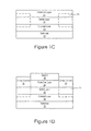
- Figures 1A-1F are cross-sectional views illustrating fabrication of a transistor according to embodiments of the present invention.
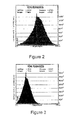
- Figures 2 and 3 are plots of Monte Carlo simulation results for the implantation of silicon into silicon nitride/aluminum gallium nitride structures.
- references herein to a layer formed "on" a substrate or other layer may refer to the layer formed directly on the substrate or other layer or on an intervening layer or layers formed on the substrate or other layer. It will also be appreciated by those of skill in the art that references to a structure or feature that is disposed "adjacent" another feature may have portions that overlap or underlie the adjacent feature.
- Embodiments of the invention are described herein with reference to cross-section illustrations that are schematic illustrations of idealized embodiments (and intermediate structures) of the invention.
- the thickness of layers and regions in the drawings may be exaggerated for clarity. Additionally, variations from the shapes of the illustrations as a result, for example, of manufacturing techniques and/or tolerances, are to be expected.
- embodiments of the invention should not be construed as limited to the particular shapes of regions illustrated herein but are to include deviations in shapes that result, for example, from manufacturing.
- an implanted region illustrated as a rectangle will, typically, have rounded or curved features and/or a gradient of implant concentration at its edges rather than a discrete change from implanted to non-implanted region.
- a buried region formed by implantation may result in some implantation in the region between the buried region and the surface through which the implantation takes place.
- the regions illustrated in the figures are schematic in nature and their shapes are not intended to illustrate the actual shape of a region of a device and are not intended to limit the scope of the invention.
- Embodiments of the present invention may be particularly well suited for use in nitride-based HEMTs such as Group III-nitride based devices.
- Group III nitride refers to those semiconducting compounds formed between nitrogen and the elements in Group III of the periodic table, usually aluminum (Al), gallium (Ga), and/or indium (In).
- Al aluminum
- Ga gallium
- In indium
- the term also refers to ternary and quaternary compounds such as AlGaN and AlInGaN.
- the Group III elements can combine with nitrogen to form binary (e.g., GaN), ternary (e.g., AlGaN, AlInN), and quaternary (e.g., AlInGaN) compounds. These compounds all have empirical formulas in which one mole of nitrogen is combined with a total of one mole of the Group III elements. Accordingly, formulas such as Al x Ga 1-x N where 0 ⁇ x ⁇ 1 are often used to describe them.
- Suitable structures for GaN-based HEMTs that may utilize embodiments of the present invention are described, for example, in commonly assigned U.S. Patent 6,316,793 and U.S. Patent Publication No. 2002/0066908A1 filed July 12, 2001 and published June 6,2002, for "ALUMINUM GALLIUM NITRIDE/GALLIUM NITRIDE HIGH ELECTRON MOBILITY TRANSISTORS HAVING A GATE CONTACT ON A GALLIUM NITRIDE BASED CAP SEGMENT AND METHODS OF FABRICATING SAME," U.S. provisional application serial no.
- embodiments of the present invention are described in connection with GaN HEMT devices, the present invention may be employed in connection with other types of devices and/or materials.
- embodiments of the invention may also be particularly suited for use in silicon carbide MESFET devices, such as the devices described in U.S. Patent No. 6,686,616 entitled "SILICON CARBIDE METAL-SEMICONDUCTOR FIELD EFFECT TRANSISTORS" the disclosure of which is hereby incorporated herein by reference in their entirety.
- some embodiments of the invention may be advantageously employed in GaN-based light emitting devices (LEDs), as well as in GaAs-based devices such as GaAs/AlGaAs pHEMT devices.
- Embodiments of the present invention utilize a protective layer during implantation of dopant atoms into a semiconductor layer, for example, to provide highly doped source/drain regions of a transistor.
- the protective layer may remain on the structure during an anneal to activate the implanted dopant atoms to protect the surface of the semiconductor layer.
- the protective layer may further remain on the semiconductor layer to act as a passivation layer for the semiconductor layer in the completed device.
- a substrate 10 is provided on which nitride based devices may be formed.
- the substrate 10 may be a semi-insulating silicon carbide (SiC) substrate that may be, for example, 4H polytype of silicon carbide.
- SiC silicon carbide
- Other silicon carbide candidate polytypes include the 3C, 6H, and 15R polytypes.
- the term "semi-insulating" is used in a relative rather absolute sense.
- the silicon carbide bulk crystal has a resistivity equal to or higher than about 1x10 5 ⁇ -cm at room temperature.
- Optional buffer, nucleation and/or transition layers may be provided on the substrate 10 .
- an AlN buffer layer may be provided to provide an appropriate crystal structure transition between the silicon carbide substrate and the remainder of the device.
- strain balancing transition layer(s) may also be provided as described, for example, in commonly assigned United States Patent Publication 2003/0102482A1 entitled “STRAIN BALANCED NITRIDE HETROJUNCTION TRANSISTORS AND METHODS OF FABRICATING STRAIN BALANCED NITRIDE HETEROJUNCTION TRANSISTORS, and United States Provisional Patent Application Serial No. 60/337,687, filed December 3,2001 and entitled "STRAIN BALANCED NITRIDE HETEROJUNCTION TRANSISTOR,” the disclosures of which are incorporated herein by reference as if set forth fully herein.
- Silicon carbide has a much closer crystal lattice match to Group III nitrides than does sapphire (Al 2 O 3 ), which is a very common substrate material for Group III nitride devices. The closer lattice match may result in Group III nitride films of higher quality than those generally available on sapphire. Silicon carbide also has a very high thermal conductivity so that the total output power of Group III nitride devices on silicon carbide is, typically, not as limited by thermal dissipation of the substrate as in the case of the same devices formed on sapphire. Also, the availability of semi-insulating silicon carbide substrates may provide for device isolation and reduced parasitic capacitance.
- SiC substrates are manufactured by, for example, Cree, Inc., of Durham, N.C., the assignee of the present invention, and methods for producing are described, for example, in U. S. Patent Nos. Re. 34,861 ; 4,946,547 ; 5,200,022 ; and 6,218,680 , the disclosures of which are incorporated herein by reference in their entirety.
- techniques for epitaxial growth of Group III nitrides have been described in, for example, U. S. Patent Nos. 5,210,051 ; 5,393,993 ; 5,523,589 ; and 5,292,501 , the disclosures of which are also incorporated herein by reference in their entirety.
- silicon carbide may be used as a substrate material
- embodiments of the present invention may utilize any suitable substrate, such as sapphire, aluminum nitride, aluminum gallium nitride, gallium nitride, silicon, GaAs, LGO, ZnO, LAO, InP and the like.
- an appropriate buffer layer also may be formed.
- a channel layer 20 is provided on the substrate 10 .
- the channel layer 20 may be deposited on the substrate 10 using buffer layers, transition layers, and/or nucleation layers as described above.
- the channel layer 20 may be under compressive strain.
- the channel layer and/or buffer nucleation and/or transition layers may be deposited by MOCVD or by other techniques known to those of skill in the art, such as MBE or HVPE.
- the channel layer 20 is a Group III-nitride, such as Al x Ga 1-x N where 0 ⁇ x ⁇ 1, provided that the energy of the conduction band edge of the channel layer 20 is less than the energy of the conduction band edge of the barrier layer 22 at the interface between the channel and barrier layers.
- x 0, indicating that the channel layer 20 is GaN.
- the channel layer 20 may also be other Group III-nitrides such as InGaN, AlInGaN or the like.
- the channel layer 20 may be undoped ("unintentionally doped") and may be grown to a thickness of greater than about 20 ⁇ .
- the channel layer 20 may also be a multi-layer structure, such as a superlattice or combinations of GaN, AlGaN or the like.
- a barrier layer 22 is provided on the channel layer 20 .
- the channel layer 20 may have a bandgap that is less than the bandgap of the barrier layer 22 and the channel layer 20 may also have a larger electron affinity than the barrier layer 22 .
- the barrier layer 22 may be deposited on the channel layer 20 .
- the barrier layer 22 is AlN, AlInN, AlGaN or AlInGaN with a thickness of between about 0.1 nm and about 10 nm. Examples of layers according to certain embodiments of the present invention are described in United States Patent Publication No. 2002/0167023A1, to Smorchkova et al.
- the barrier layer 22 is thick enough and has a high enough Al composition and doping to induce a significant carrier concentration at the interface between the channel layer 20 and the barrier layer 22 through polarization effects when the barrier layer 22 is buried under ohmic contact metal.
- the barrier layer 22 should be thick enough to reduce or minimize scattering of electrons in the channel due to ionized impurities deposited at the interface between the barrier layer 22 and a protective 24 (Fig. 1B) .
- the barrier layer 22 may have a bandgap larger than that of the channel layer 20 and a smaller electron affinity than the channel layer 20 .
- the barrier layer 22 may include AlGaN, AlInGaN and/or AlN or combinations of layers thereof.
- the barrier layer 22 may, for example, be from about 0.1 nm to about 10 nm thick, but should not be so thick as to cause cracking or substantial defect formation therein.
- the barrier layer 22 is undoped or doped with an n-type dopant to a concentration less than about 1x10 19 cm -3 .
- the barrier layer 22 is Al x Ga 1-x N where 0 ⁇ x ⁇ 1.
- the aluminum concentration is about 25%.
- the barrier layer 22 comprises AlGaN with an aluminum concentration of between about 5% and about 100%.
- the aluminum concentration is greater than about 10%.
- a protective layer 24 is formed on the barrier layer 22 .
- the protective layer 24 may be silicon nitride (Si x N y ), silicon dioxide (SiO 2 ) and/or another suitable protective material, such as silicon oxynitride (SiON).
- Si x N y silicon dioxide
- SiON silicon oxynitride
- the terms "Si x N y ,” “SiN” and “silicon nitride” are used herein interchangeably to refer to both stoichiometric and non-stoichimetric silicon nitride.
- Other materials may also be utilized for the protective layer 24 .
- the protective layer 24 could also include magnesium oxide, scandium oxide, aluminum oxide and/or aluminum oxynitride.
- the protective layer 24 may be a single layer or multiple layers of uniform and/or non-uniform composition.
- the material of the protective layer 24 should have appropriate interface characteristics, should be capable of withstanding relatively high temperatures, and should be capable of being removed without significantly damaging the underlying barrier layer 22 .
- the protective layer 24 may be a dielectric layer that has a relatively high breakdown field strength and that provides a relatively low interface trap density at the interface with an underlying Group III-nitride layer such as the barrier layer 22 .
- the protective layer 24 may have a high etch selectivity with respect to the material of the barrier layer 22 , and may not be reactive to the material of the barrier layer 22 .
- the protective layer 24 may have a relatively low level of impurities therein.
- the protective layer 24 may have a relatively low level of hydrogen and other impurities, including oxygen, carbon, fluorine and chlorine.
- the protective layer 24 may be stable at relatively high temperatures (e.g. >1000 °C) in order to withstand high annealing temperatures used in subsequent process steps.
- the protective layer 24 is SiN.
- the SiN may be formed for example by Low Pressure Chemical Vapor Deposition (LPCVD) and/or Metal-Organic Chemical Vapor Deposition (MOCVD).
- LPCVD Low Pressure Chemical Vapor Deposition
- MOCVD Metal-Organic Chemical Vapor Deposition
- the SiN layer may be stoichiometric (i.e. the ratio of silicon to nitrogen in the material is about 3:4).
- the stoichiometry of a SiN layer may be adjusted, for example, by adjusting the relative flow rates of SiH 4 and NH 3 source gases in a CVD process.
- CVD-grown SiN tends to be stoichiometric.
- a SiN protective layer 24 may have an index of refraction at a 633 nm wavelength of from about 1.6 to about 2.2.
- the index of refraction of a SiN protective layer 24 is 1.98 ⁇ 0.05 as measured by ellipsometry.
- Stoichiometric SiN may also be characterized by its etch rate in a buffered oxide etch (BOE). For example, the etch rate of stoichiometric SiN in BOE is nearly zero.
- the protective layer 24 may be SiO 2 .
- the SiO 2 may be formed by LPCVD and/or MOCVD and may be stoichiometric.
- an SiO 2 protective layer may have an index of refraction at a 633 nm wavelength of from about 1.36 to about 1.56.
- the index of refraction of an SiO 2 protective layer is 1.46 ⁇ 0.03 as measured by ellipsometry.
- the protective layer 24 When the protective layer 24 includes silicon nitride, the protective layer 24 should have impurity levels at or below the levels shown in Table 1, as measured by secondary ion mass spectroscopy (SIMS) with a Cs ion beam.
- SIMS secondary ion mass spectroscopy
- the protective layer 24 may be blanket formed on the barrier layer 22 .
- the protective layer 24 may have a thickness in the range of about 100 nm, however, other thickness layers may also be utilized.
- the protective layer should be sufficiently thick so as to protect the underlying layer during a subsequent anneal of ohmic contacts. Layers as thin as two or three monolayers may be sufficient for such purposes.
- the protective layer 24 may have a thickness of from about 10 nm to about 500nm.
- the protective layer may comprise a high purity SiN layer as described in U.S. Patent Application Serial No. 11/286,805 entitled "GROUP III NITRIDE SEMICONDUCTOR DEVICES WITH SILICON NITRIDE LAYERS AND METHODS OF MANUFACTURING SUCH DEVICES" filed 23 November 2005, the disclosure of which is incorporated herein by reference as if fully set forth herein.
- an in situ grown SiN protective layer 24 may be grown at relatively high temperatures (e.g., above about 700 °C).
- the SiN layers may be grown at a temperature in the range of about 900 - 1000 °C.
- Such high temperature growth may also facilitate reducing the impurity levels in the SiN layer and at the interface between a Group III nitride layer and the SiN layer. Additionally, high growth rates may be employed which may facilitate reducing the levels of background reactor impurities incorporated into the SiN layer.
- the SiN layer(s) may be grown at a growth rate of at least about 0.2 microns/hour. In certain specific embodiments, the growth rate may be about 2 microns/hour.
- Forming the SiN layer in situ may also reduce the levels of impurities that are incorporated into the top surface of the uppermost Group III nitride layer and/or into the SiN layer itself.
- a number of different mechanisms may introduce impurities.
- the hydrogen may tend to incorporate into the Group III nitride layer during cooling of the reactor following growth.
- impurities may be introduced, particularly adjacent the outer surfaces of the device, as a result of handling of the device and/or chemical cleaning of the device.
- Impurities may also be added if post-growth processing such as wet etching, electrode deposition, annealing steps, etc. are performed prior to deposition of the SiN protective/passivation layer.
- These impurities may change the surface states at the interface between the Group III nitride layer and the SiN layer in ways that may be undesirable and/or difficult to control/reproduce.
- the presence of impurities can increase trapping at the interface between the SiN layer and the underlying Group III nitride layer, thereby increasing the sheet resistance of the channel.
- high purity silane may be used as a source gas in the growth of the SiN layer(s).
- silane is often used as a source for silicon dopants in the growth of n-doped Group III nitride layers.
- diluted silane gas is used in such applications as it is less expensive and easier to use than pure silane, which may be highly combustible.
- the use of such pure silane may facilitate reducing the level of impurities at, for example, the interface between the Group III nitride layer and the SiN layer and/or within the SiN layer, which may, in certain circumstances, improve the performance and/or reproducibility of the device.
- the higher quality (i.e., more pure) SiN layer may help reduce or minimize trapping within the body of the insulative layer, thereby providing a higher breakdown critical field.
- a pure silane gas source it may still be desirable to include a diluted silane source as well, so that diluted silane gas may be used as the dopant gas source during the growth of, for example, an n-doped or co-doped Group III nitride layer.
- a mask 25 is formed on the protective layer 24 .
- the mask 25 may include photoresist or any other suitable mask material such as SiN and/or SiO 2 .
- the mask may have a thickness selected to block implanted ions.
- the protective layer comprises SiN
- the mask 25 may include an oxide such as SiO 2 , and vice-versa.
- Windows are opened in the mask 25 to expose surface portions 24A of the protective layer 24 , and impurity ions 27 are implanted through the windows into the protective layer 24 such that at least a portion of the implanted ions come to rest within the barrier layer 22 .
- some of the implanted ions may come to rest within the channel layer 20 .
- the implanted ions form a concentration profile having a peak near the interface 29 between the protective layer 24 and the barrier layer 22 .
- the implant peak may be placed away from (i.e. above or below) the interface 29 between the protective layer 24 and the barrier layer 22 .
- an implanted region 31 may be formed partially within the protective layer 24 , the barrier layer 22 and/or the channel layer 20 .
- the implant conditions may be selected to provide an implanted region 31 having a peak dopant concentration of 1x10 18 cm -3 or greater.
- the dose and energy of the implants may be selected to provide a peak dopant concentration of about 5x10 19 cm -3 .
- the implant process may include multiple implant steps to provide a net profile of implanted dopants.
- the implant process may include a first implant step performed under a first set of implant conditions and a subsequent implant step performed under a second set of implant conditions. More than two implant steps may be performed.
- the implants may be performed at room temperature.
- the implant energies and dose may be selected to provide an implant profile that achieves a desired sheet resistivity and/or permits fabrication of low resistivity ohmic contacts to the barrier layer 22 as provided below.
- the implanted ions may include silicon, sulfur and/or oxygen ions.
- the implants may be activated by an activation anneal.
- the mask 25 may be removed prior to the implant activation anneal, for example by means of a photoresist strip and/or an etch process.
- the activation anneal may be performed with the protective layer 24 in place.
- the protective layer 24 may protect the surface of the barrier layer 22 during the anneal.
- the activation anneal may be performed in an inert atmosphere including, for example, N 2 and/or Ar.
- the anneal atmosphere may include a partial pressure of NH 3 in the range of about 0.1mbar to 1000mbar. More particularly, the NH 3 may have a pressure of about 10 - 100 mbar. In particular, the NH 3 may have a pressure of about 90mbar.
- the NH 3 may help to reduce decomposition of the SiN protective layer 24 .
- the activation anneal may be performed at a temperature sufficient to activate the implanted dopant ions but less than a temperature at which the underlying semiconductor layer, i.e. the barrier layer 22 , deteriorates.
- the presence of the protective layer 24 during the high temperature process steps may inhibit damage to the underlying epitaxial layers, including barrier layer 22 , that may otherwise result from high temperature annealing.
- the activation anneal may be performed at a temperature greater than 1000°C.
- SiH 4 may be provided during the implant anneal along with NH 3 , in which case, SiN may be deposited on the protective layer during the anneal.
- the activation anneal may be performed at a temperature of about 1000 °C to about 1300 °C.
- the activation anneal may be performed in-situ and/or in a separate annealing chamber.
- the activation anneal may be performed for at least about 30 seconds or more, depending on the anneal temperature.
- a rapid thermal anneal (RTA) at about 1300 °C may be performed for about 30 seconds
- a furnace anneal at about 1000 °C may be performed for about 30 minutes.
- the particular selection of activation times and temperatures may vary depending on the type of materials involved and the particular implant conditions employed.
- the anneal time may be in the range of about 30 seconds to about 30 minutes.
- a second mask 35 is formed on the protective layer, and windows are then opened in the protective layer 24 for the formation ofohmic contacts 30 .
- the windows may be formed utilizing a low damage etch with respect to the barrier layer 22 to expose the underlying barrier layer 22 .
- low damage etch techniques include etching techniques other than reactive ion etching, such as inductively coupled plasma or electron cyclotron resonance (ECR) or downstream plasma etching with no DC component to the plasma.
- ECR electron cyclotron resonance
- a low damage etch could be a wet etch with buffered hydrofluoric acid.
- the protective layer 24 may include the SiN and/or SiO 2 layer as well as the etch stop layer.
- the protective layer 24 may include multiple layers.
- Metal may then be deposited, for example by evaporation, in the windows to provide the ohmic contacts 30 .
- Suitable metals may include Ti, Si, Ni, Au, Al, Ta, Mo, TiN, WSiN, and/or Pt. If it is desired to anneal the deposited metal to form ohmic contacts, a separate lithography step may be performed such that the ohmic contacts 30 are pattemed so as to be smaller than the window in the protective layer 24 .
- the edges of the ohmic contacts 30 may thereby be spaced apart from the protective layer 24 .
- the edges of the ohmic contacts 30 may be spaced apart from the protective layer 24 by a distance in the range of about 0.1 to about 0.2 ⁇ m.
- the ohmic contacts 30 may be spaced apart from the protective layer 24 a distance sufficiently large to allow for misalignment tolerances in the formation and patterning of the ohmic contact metal. If the ohmic contact metal contacts the protective layer 24 , the metal may diffuse into the protective layer 24 during subsequent heating steps which may result in a short between a gate contact and the ohmic contact(s) 30 .
- the gap between the ohmic contacts 30 and the protective layer 24 should not be so large as to defeat the protective purpose of the protective layer 24 and, thereby, substantially degrade the performance of the device but should not be so small to risk random contact of ohmic material to the protective layer.
- the gap may be from about 0.1 ⁇ m to about 0.5 ⁇ m.
- the deposited metal may be annealed to provide the ohmic contacts 30 .
- the anneal may be a high temperature anneal.
- the anneal may be an anneal at a temperature of greater than about 900 °C in an atmosphere of an inert gas such as N 2 or Ar.
- an ohmic contact anneal the resistance of the ohmic contacts may be reduced from a relatively high resistance to about 1 ⁇ -mm or less.
- the term "ohmic contact” refers to a non-rectifying contact that has a contact resistance of about 1 ⁇ -mm or less.
- the presence of the protective layer 24 during the high temperature process steps may inhibit damage to the barrier layer 22 that may otherwise be caused by such steps.
- the sheet resistance of the gate region 21 after the high temperature ohmic contact anneal may be substantially the same as the sheet resistance of the gate region 21 as-grown ( i.e. before the contact anneal).
- the metal may be ohmic as deposited. Since a contact anneal may not be required, it may be acceptable for the metal of the ohmic contacts 30 to contact the protective layer 24 .
- a lithography step that may otherwise be required in order to ensure that the ohmic contacts 30 are spaced away from the protective layer 24 may be avoided as a result of the implantation of impurities into the barrier layer 22 .
- the ohmic contacts 30 are formed on the implanted regions 31 , the ohmic contacts may have a lower resistivity than ohmic contacts formed on non-implanted regions. Thus, the on-resistance of devices formed according to some embodiments of the invention may be lowered.
- improved ohmic contacts in GaN HEMTs may help improve the performance of power amplifiers at mm-wave frequencies, as well as other applications that require low on-resistance, including, for example, RF power switches, limiters, and cascode cells.
- reducing the contact resistance of the device may permit an increase in the drain-source spacing without increasing the on-resistance of the device.
- Figure 1E illustrates the formation of a gate contact 32.
- a mask (not shown) is formed on the ohmic contacts and the protective layer 24 and patterned to form a window that exposes a portion of the protective layer 24 .
- a recess is then formed through the protective layer 24 to expose a portion of the barrier layer 22 .
- the recess is formed using a low damage etch process as described above.
- the recess may be offset between the source and drain contacts such that the recess, and subsequently the gate contact 32 , is closer to the source contact than the drain contact.
- a gate contact 32 is formed in the recess and contacts the exposed portion of the barrier layer 22 .
- the gate contact may be a "T" gate as illustrated in Figure 1E and may be fabricated using conventional fabrication techniques. Suitable gate materials may depend on the composition of the barrier layer, however, in certain embodiments, conventional materials capable of making a Schottky contact to a nitride based semiconductor material may be used, such as Ni, Pt, NiSi x , Cu, Pd, Cr, W and/or WSiN.
- a small gap between the protective layer 24 and the gate contact 32 may arise as a result of, for example, anisotropy of the low-damage etch, resulting in an exposed surface of the barrier layer 22 between the protective layer 24 and the gate contact 32 .
- the source/drain contacts may not need to be annealed, it may be possible to form the source and drain contacts using the same metal in a single metallization step.
- Ti, Si, Ni, Au, Al, Ta, Mo, TiN, WSiN, and/or Pt may form an ohmic contact as-deposited on the doped regions 31 of the barrier layer 22 while forming a non-ohmic contact on other portions of the barrier layer 22 .
- Figure 1F illustrates the formation of a passivation layer 34 .
- the passivation layer may be blanket deposited on the structure of Figure 1E .
- the passivation layer 34 is deposited so as to substantially fill a gap between the protective layer 24 and the ohmic contacts 30 and also a gap between the protective layer 24 and the gate contact 32 , if such gap(s) exist.
- the passivation layer 34 may be silicon nitride, aluminum nitride, silicon dioxide and/or an oxynitride.
- the passivation layer 34 may be a single or multiple layers of uniform and/or non-uniform composition.
- Figure 2 is a plot of Monte Carlo simulation results for a possible impurity profile for silicon ions implanted into a structure including 100 nm of SiN on GaN.
- the simulation results are based on an implantation energy of 120 keV, which results in a peak concentration near the SiN/GaN interface.
- a dose of about 3.4x10 14 ions/cm 2 would result in a peak concentration of 5x10 19 cm -3 near the SiN/GaN interface.
- Figure 3 is a plot of Monte Carlo simulation results for a possible impurity profile for silicon ions implanted into a structure including 30 mn of SiN on GaN. According to the simulation results, an implantation energy of 35 keV results in a peak concentration near the SiN/GaN interface. According to the simulation, for a peak concentration of 5x10 19 cm -3 , a dose of about 1.5x10 14 ions/cm 2 would be acceptable.
- the best combination of energy/dose may depend on the activation anneal that is used, which may be optimized for a given structure. However, it is presently believed that implant dose may have a greater effect on the resulting structure than anneal temperature.
- the implant dose may be about 4x10 14 ions/cm 2 or greater. In some embodiments, the implant dose may be greater than about 2x10 15 ions/cm 2 .
- the peak implant concentration may be greater than about 1x10 20 cm -3 . In some cases, the peak implant concentration may be greater than about 3x10 20 cm -3 .
- a dose of 2.4x10 15 ions/cm 2 implanted at 130 keV would result in a peak volumetric concentration of about 3.4x10 20 cm -3 , which may be desirable for some applications.
- the dose should be at least about 4x10 14 /cm 2 , but higher doses may be preferred because it may lead to good activation at lower anneal temperatures.
- additional layers may be included in the HEMT device while still benefiting from the teachings of the present invention.
- additional layers may include GaN cap layers, as for example, described in Yu et al., "Schottky barrier engineering in III-V nitrides via the piezoelectric effect," Applied Physics Letters, Vol. 73, No. 13, 1998 , or in U.S. Patent Publication No.
- insulating layers such as SiN, or relatively high quality AlN may be deposited for making a MISHEMT and/or passivating the surface.
- the additional layers may also include a compositionally graded transition layer or layers.
- the barrier layer 22 may also be provided with multiple layers as described in United States Patent Publication No. 2002/0167023A1, to Smorchkova et al. , entitled "GROUP-III NITRIDE BASED HIGH ELECTRON MOBILITY TRANSISTOR (HEMT) WITH BARRIER/SPACER LAYER" the disclosure of which is incorporated herein by reference as if set forth fully herein.
- embodiments of the present invention should not be construed as limiting the barrier layer to a single layer but may include, for example, barrier layers having combinations of GaN, AlGaN and/or AlN layers.
- a GaN, AlN structure may be utilized to reduce or prevent alloy scattering.
- embodiments of the present invention may include nitride based barrier layers, such nitride based barrier layers may include AlGaN based barrier layers, AlN based barrier layers and combinations thereof.
Landscapes
- Engineering & Computer Science (AREA)
- Microelectronics & Electronic Packaging (AREA)
- Power Engineering (AREA)
- Physics & Mathematics (AREA)
- Condensed Matter Physics & Semiconductors (AREA)
- General Physics & Mathematics (AREA)
- Computer Hardware Design (AREA)
- Manufacturing & Machinery (AREA)
- Ceramic Engineering (AREA)
- High Energy & Nuclear Physics (AREA)
- Chemical & Material Sciences (AREA)
- Crystallography & Structural Chemistry (AREA)
- Toxicology (AREA)
- Health & Medical Sciences (AREA)
- Junction Field-Effect Transistors (AREA)
- Electrodes Of Semiconductors (AREA)
- Formation Of Insulating Films (AREA)
- Recrystallisation Techniques (AREA)
Applications Claiming Priority (1)
| Application Number | Priority Date | Filing Date | Title |
|---|---|---|---|
| US11/302,062 US7419892B2 (en) | 2005-12-13 | 2005-12-13 | Semiconductor devices including implanted regions and protective layers and methods of forming the same |
Publications (3)
| Publication Number | Publication Date |
|---|---|
| EP1798762A2 true EP1798762A2 (fr) | 2007-06-20 |
| EP1798762A3 EP1798762A3 (fr) | 2008-12-10 |
| EP1798762B1 EP1798762B1 (fr) | 2013-01-23 |
Family
ID=37857147
Family Applications (1)
| Application Number | Title | Priority Date | Filing Date |
|---|---|---|---|
| EP06126051A Active EP1798762B1 (fr) | 2005-12-13 | 2006-12-13 | Méthode pour la fabrication de dispositifs semiconducteur comprenant des régions implantées et des couches de protection |
Country Status (3)
| Country | Link |
|---|---|
| US (2) | US7419892B2 (fr) |
| EP (1) | EP1798762B1 (fr) |
| JP (2) | JP5295496B2 (fr) |
Cited By (9)
| Publication number | Priority date | Publication date | Assignee | Title |
|---|---|---|---|---|
| WO2009117045A1 (fr) * | 2008-03-19 | 2009-09-24 | Cree, Inc. | Dispositifs à base de nitrure et de carbure de silicium intégrés et procédés de fabrication de dispositifs à base de nitrure intégrés |
| EP2031648A3 (fr) * | 2007-08-28 | 2010-02-24 | Cree, Inc. | Passivation de dispositifs semiconducteurs de type large bande interdite à l'aide de nitrures pulvérisés dépourvus d'hydrogène |
| EP2246880A1 (fr) * | 2008-02-22 | 2010-11-03 | Eudyna Devices Inc. | Procédé de fabrication d'un dispositif semi-conducteur |
| US7858460B2 (en) | 2005-06-29 | 2010-12-28 | Cree, Inc. | Passivation of wide band-gap based semiconductor devices with hydrogen-free sputtered nitrides |
| US7875910B2 (en) | 2003-03-03 | 2011-01-25 | Cree, Inc. | Integrated nitride and silicon carbide-based devices |
| US8994073B2 (en) | 2012-10-04 | 2015-03-31 | Cree, Inc. | Hydrogen mitigation schemes in the passivation of advanced devices |
| WO2017137291A2 (fr) | 2016-02-08 | 2017-08-17 | Abb Schweiz Ag | Procédé de fabrication d'un dispositif à semi-conducteurs comprenant un contact auto-aligné vers une région de puits dopée |
| US9812338B2 (en) | 2013-03-14 | 2017-11-07 | Cree, Inc. | Encapsulation of advanced devices using novel PECVD and ALD schemes |
| US9991399B2 (en) | 2012-10-04 | 2018-06-05 | Cree, Inc. | Passivation structure for semiconductor devices |
Families Citing this family (117)
| Publication number | Priority date | Publication date | Assignee | Title |
|---|---|---|---|---|
| JP4897948B2 (ja) * | 2005-09-02 | 2012-03-14 | 古河電気工業株式会社 | 半導体素子 |
| JP2007235000A (ja) * | 2006-03-03 | 2007-09-13 | Eudyna Devices Inc | 半導体の処理方法、半導体装置およびその製造方法 |
| US9040398B2 (en) * | 2006-05-16 | 2015-05-26 | Cree, Inc. | Method of fabricating seminconductor devices including self aligned refractory contacts |
| US7656010B2 (en) * | 2006-09-20 | 2010-02-02 | Panasonic Corporation | Semiconductor device |
| JP2008135700A (ja) * | 2006-11-01 | 2008-06-12 | Furukawa Electric Co Ltd:The | Iii族窒化物膜の製造方法及びiii族窒化物半導体素子 |
| WO2008061085A1 (fr) * | 2006-11-10 | 2008-05-22 | University Of South Carolina | Semi-conducteurs à dopage sélectif et leurs procédés de fabrication |
| JP5200372B2 (ja) * | 2006-12-07 | 2013-06-05 | 日立電線株式会社 | 電界効果トランジスタおよびその製造方法 |
| JP5347228B2 (ja) * | 2007-03-05 | 2013-11-20 | 日本電気株式会社 | 電界効果トランジスタ |
| WO2008112185A1 (fr) * | 2007-03-09 | 2008-09-18 | The Regents Of The University Of California | Procédé de fabrication de transistors à effet de champ à composé du groupe iii-n en utilisant une implantation ionique avec une activation de dopant réduite et une température de reprise détériorée |
| KR100851758B1 (ko) * | 2007-03-14 | 2008-08-11 | 동부일렉트로닉스 주식회사 | 이미지 센서 및 그의 제조방법 |
| US8035130B2 (en) * | 2007-03-26 | 2011-10-11 | Mitsubishi Electric Corporation | Nitride semiconductor heterojunction field effect transistor having wide band gap barrier layer that includes high concentration impurity region |
| FR2914500B1 (fr) * | 2007-03-30 | 2009-11-20 | Picogiga Internat | Dispositif electronique a contact ohmique ameliore |
| US8502323B2 (en) * | 2007-08-03 | 2013-08-06 | The Hong Kong University Of Science And Technology | Reliable normally-off III-nitride active device structures, and related methods and systems |
| US7875537B2 (en) * | 2007-08-29 | 2011-01-25 | Cree, Inc. | High temperature ion implantation of nitride based HEMTs |
| US7750370B2 (en) | 2007-12-20 | 2010-07-06 | Northrop Grumman Space & Mission Systems Corp. | High electron mobility transistor having self-aligned miniature field mitigating plate on a protective dielectric layer |
| US8497527B2 (en) * | 2008-03-12 | 2013-07-30 | Sensor Electronic Technology, Inc. | Device having active region with lower electron concentration |
| US8519438B2 (en) | 2008-04-23 | 2013-08-27 | Transphorm Inc. | Enhancement mode III-N HEMTs |
| US9711633B2 (en) * | 2008-05-09 | 2017-07-18 | Cree, Inc. | Methods of forming group III-nitride semiconductor devices including implanting ions directly into source and drain regions and annealing to activate the implanted ions |
| EP2117039B1 (fr) | 2008-05-09 | 2015-03-18 | Cree, Inc. | Dispositifs semi-conducteurs incluant des régions implantées peu profondes et leurs procédés de formation |
| JP5463529B2 (ja) * | 2008-06-11 | 2014-04-09 | 古河電気工業株式会社 | 電界効果トランジスタの製造方法 |
| JP5432480B2 (ja) * | 2008-07-02 | 2014-03-05 | ルネサスエレクトロニクス株式会社 | Si基板上のGaN系デバイスの熱処理方法 |
| US7985986B2 (en) * | 2008-07-31 | 2011-07-26 | Cree, Inc. | Normally-off semiconductor devices |
| US8289065B2 (en) | 2008-09-23 | 2012-10-16 | Transphorm Inc. | Inductive load power switching circuits |
| US20100084687A1 (en) * | 2008-10-03 | 2010-04-08 | The Hong Kong University Of Science And Technology | Aluminum gallium nitride/gallium nitride high electron mobility transistors |
| JP2010098194A (ja) * | 2008-10-17 | 2010-04-30 | Meijo Univ | 蛍光体、発光素子、発光装置及び蛍光体の製造方法 |
| US7977224B2 (en) * | 2008-12-03 | 2011-07-12 | The United States Of America As Represented By The Secretary Of The Army | Method using multiple layer annealing cap for fabricating group III-nitride semiconductor device structures and devices formed thereby |
| US7898004B2 (en) | 2008-12-10 | 2011-03-01 | Transphorm Inc. | Semiconductor heterostructure diodes |
| JP5323527B2 (ja) * | 2009-02-18 | 2013-10-23 | 古河電気工業株式会社 | GaN系電界効果トランジスタの製造方法 |
| US8742459B2 (en) | 2009-05-14 | 2014-06-03 | Transphorm Inc. | High voltage III-nitride semiconductor devices |
| WO2010151856A2 (fr) * | 2009-06-26 | 2010-12-29 | Cornell University | Dépôt chimique en phase vapeur pour nitrure daluminium et de silicium |
| US8105889B2 (en) * | 2009-07-27 | 2012-01-31 | Cree, Inc. | Methods of fabricating transistors including self-aligned gate electrodes and source/drain regions |
| US8390000B2 (en) | 2009-08-28 | 2013-03-05 | Transphorm Inc. | Semiconductor devices with field plates |
| KR101079203B1 (ko) * | 2009-09-28 | 2011-11-03 | 주식회사 하이닉스반도체 | 반도체 장치의 게이트 패턴 및 그의 제조 방법 |
| US8389977B2 (en) | 2009-12-10 | 2013-03-05 | Transphorm Inc. | Reverse side engineered III-nitride devices |
| KR101116356B1 (ko) | 2010-01-29 | 2012-03-09 | 주식회사 하이닉스반도체 | 플라즈마 도핑 방법 및 그를 이용한 반도체장치 제조 방법 |
| JP5685020B2 (ja) * | 2010-07-23 | 2015-03-18 | 住友電気工業株式会社 | 半導体装置の製造方法 |
| JP2012033689A (ja) * | 2010-07-30 | 2012-02-16 | Sumitomo Electric Device Innovations Inc | 半導体装置の製造方法 |
| US8742460B2 (en) | 2010-12-15 | 2014-06-03 | Transphorm Inc. | Transistors with isolation regions |
| KR101827514B1 (ko) * | 2011-08-18 | 2018-02-08 | 주성엔지니어링(주) | 박막 트랜지스터 및 그 제조 방법 |
| US8643062B2 (en) | 2011-02-02 | 2014-02-04 | Transphorm Inc. | III-N device structures and methods |
| US8772842B2 (en) | 2011-03-04 | 2014-07-08 | Transphorm, Inc. | Semiconductor diodes with low reverse bias currents |
| US8716141B2 (en) | 2011-03-04 | 2014-05-06 | Transphorm Inc. | Electrode configurations for semiconductor devices |
| JP2013021242A (ja) | 2011-07-14 | 2013-01-31 | Sumitomo Electric Ind Ltd | 半導体装置の製造方法 |
| JP5845714B2 (ja) * | 2011-08-19 | 2016-01-20 | 住友電気工業株式会社 | 炭化珪素半導体装置の製造方法 |
| US8901604B2 (en) | 2011-09-06 | 2014-12-02 | Transphorm Inc. | Semiconductor devices with guard rings |
| US9257547B2 (en) | 2011-09-13 | 2016-02-09 | Transphorm Inc. | III-N device structures having a non-insulating substrate |
| US8598937B2 (en) | 2011-10-07 | 2013-12-03 | Transphorm Inc. | High power semiconductor electronic components with increased reliability |
| US20130105817A1 (en) | 2011-10-26 | 2013-05-02 | Triquint Semiconductor, Inc. | High electron mobility transistor structure and method |
| EP2602827B1 (fr) * | 2011-12-09 | 2016-02-03 | Imec | Dispositif au nitrure du groupe III à mode d'enrichissement et son procédé de fabrication |
| US9165766B2 (en) | 2012-02-03 | 2015-10-20 | Transphorm Inc. | Buffer layer structures suited for III-nitride devices with foreign substrates |
| KR101256466B1 (ko) * | 2012-02-06 | 2013-04-19 | 삼성전자주식회사 | 질화물계 이종접합 반도체 소자 및 그 제조 방법 |
| JP5750382B2 (ja) * | 2012-02-15 | 2015-07-22 | シャープ株式会社 | 窒化物半導体装置 |
| CN102570305B (zh) * | 2012-03-06 | 2013-04-17 | 中国科学院半导体研究所 | 基于硅基赝砷化镓衬底的850nm激光器的制备方法 |
| US9640627B2 (en) | 2012-03-07 | 2017-05-02 | Cree, Inc. | Schottky contact |
| JP5715588B2 (ja) * | 2012-03-28 | 2015-05-07 | 株式会社東芝 | 半導体装置およびその製造方法 |
| JP5701805B2 (ja) * | 2012-03-28 | 2015-04-15 | 株式会社東芝 | 窒化物半導体ショットキダイオードの製造方法 |
| JP6054620B2 (ja) * | 2012-03-29 | 2016-12-27 | トランスフォーム・ジャパン株式会社 | 化合物半導体装置及びその製造方法 |
| US9093366B2 (en) | 2012-04-09 | 2015-07-28 | Transphorm Inc. | N-polar III-nitride transistors |
| US9184275B2 (en) | 2012-06-27 | 2015-11-10 | Transphorm Inc. | Semiconductor devices with integrated hole collectors |
| US9076763B2 (en) * | 2012-08-13 | 2015-07-07 | Infineon Technologies Austria Ag | High breakdown voltage III-nitride device |
| JP6085442B2 (ja) | 2012-09-28 | 2017-02-22 | トランスフォーム・ジャパン株式会社 | 化合物半導体装置及びその製造方法 |
| US9202703B2 (en) | 2012-11-05 | 2015-12-01 | Cree, Inc. | Ni-rich Schottky contact |
| US9425276B2 (en) * | 2013-01-21 | 2016-08-23 | Taiwan Semiconductor Manufacturing Co., Ltd. | High electron mobility transistors |
| US9171730B2 (en) | 2013-02-15 | 2015-10-27 | Transphorm Inc. | Electrodes for semiconductor devices and methods of forming the same |
| US9087718B2 (en) | 2013-03-13 | 2015-07-21 | Transphorm Inc. | Enhancement-mode III-nitride devices |
| US9245992B2 (en) | 2013-03-15 | 2016-01-26 | Transphorm Inc. | Carbon doping semiconductor devices |
| JPWO2014203881A1 (ja) * | 2013-06-21 | 2017-02-23 | 富士電機株式会社 | 炭化珪素半導体素子の製造方法 |
| US9443938B2 (en) | 2013-07-19 | 2016-09-13 | Transphorm Inc. | III-nitride transistor including a p-type depleting layer |
| JP6241915B2 (ja) * | 2013-07-31 | 2017-12-06 | 住友電工デバイス・イノベーション株式会社 | 半導体装置の製造方法 |
| JP2015073073A (ja) * | 2013-09-06 | 2015-04-16 | 三菱電機株式会社 | 半導体装置およびその製造方法 |
| KR102086360B1 (ko) * | 2013-11-07 | 2020-03-09 | 삼성전자주식회사 | n형 질화물 반도체의 전극형성방법, 질화물 반도체 소자 및 그 제조방법 |
| US9306014B1 (en) * | 2013-12-27 | 2016-04-05 | Power Integrations, Inc. | High-electron-mobility transistors |
| US10276712B2 (en) | 2014-05-29 | 2019-04-30 | Hrl Laboratories, Llc | III-nitride field-effect transistor with dual gates |
| US9318593B2 (en) | 2014-07-21 | 2016-04-19 | Transphorm Inc. | Forming enhancement mode III-nitride devices |
| FR3026557B1 (fr) * | 2014-09-26 | 2018-03-16 | Commissariat A L'energie Atomique Et Aux Energies Alternatives | Procede de dopage d'un semi-conducteur a base de gan |
| CN104576317A (zh) * | 2014-12-15 | 2015-04-29 | 中国电子科技集团公司第五十五研究所 | 一种采用AlGaN沟道层的异质结材料的生长方法 |
| US9536967B2 (en) | 2014-12-16 | 2017-01-03 | Transphorm Inc. | Recessed ohmic contacts in a III-N device |
| US9536966B2 (en) | 2014-12-16 | 2017-01-03 | Transphorm Inc. | Gate structures for III-N devices |
| US9812532B1 (en) * | 2015-08-28 | 2017-11-07 | Hrl Laboratories, Llc | III-nitride P-channel transistor |
| US20170069723A1 (en) * | 2015-09-08 | 2017-03-09 | M/A-Com Technology Solutions Holdings, Inc. | Iii-nitride semiconductor structures comprising multiple spatially patterned implanted species |
| JP6623691B2 (ja) * | 2015-10-30 | 2019-12-25 | 富士通株式会社 | 化合物半導体装置及びその製造方法 |
| CN108292678B (zh) | 2015-11-19 | 2021-07-06 | Hrl实验室有限责任公司 | 具有双栅极的iii族氮化物场效应晶体管 |
| JP6888013B2 (ja) | 2016-01-15 | 2021-06-16 | トランスフォーム テクノロジー,インコーポレーテッド | AL(1−x)Si(x)Oゲート絶縁体を有するエンハンスメントモードIII族窒化物デバイス |
| US10541323B2 (en) | 2016-04-15 | 2020-01-21 | Macom Technology Solutions Holdings, Inc. | High-voltage GaN high electron mobility transistors |
| US10985284B2 (en) | 2016-04-15 | 2021-04-20 | Macom Technology Solutions Holdings, Inc. | High-voltage lateral GaN-on-silicon schottky diode with reduced junction leakage current |
| US10229839B2 (en) | 2016-04-29 | 2019-03-12 | The United States Of America, As Represented By The Secretary Of The Navy | Transition metal-bearing capping film for group III-nitride devices |
| WO2017210323A1 (fr) | 2016-05-31 | 2017-12-07 | Transphorm Inc. | Dispositifs au nitrure du groupe iii comprenant une couche d'appauvrissement à gradient |
| US10354879B2 (en) * | 2016-06-24 | 2019-07-16 | Cree, Inc. | Depletion mode semiconductor devices including current dependent resistance |
| JP6896063B2 (ja) | 2016-08-18 | 2021-06-30 | レイセオン カンパニー | イオン注入を用いた高抵抗窒化物バッファ層の半導体材料成長 |
| JP6618944B2 (ja) | 2017-03-10 | 2019-12-11 | 株式会社東芝 | 半導体装置及び電気装置 |
| JP2018163928A (ja) * | 2017-03-24 | 2018-10-18 | 住友電気工業株式会社 | 半導体装置の製造方法 |
| US10388753B1 (en) * | 2017-03-31 | 2019-08-20 | National Technology & Engineering Solutions Of Sandia, Llc | Regrowth method for fabricating wide-bandgap transistors, and devices made thereby |
| TWI618244B (zh) * | 2017-06-06 | 2018-03-11 | Huang Zhi Shu | N-face III族/氮化物磊晶結構及其主動元件與其積體化之極性反轉製作方法 |
| US11699704B2 (en) * | 2017-09-28 | 2023-07-11 | Intel Corporation | Monolithic integration of a thin film transistor over a complimentary transistor |
| US10950598B2 (en) | 2018-01-19 | 2021-03-16 | Macom Technology Solutions Holdings, Inc. | Heterolithic microwave integrated circuits including gallium-nitride devices formed on highly doped semiconductor |
| US11233047B2 (en) | 2018-01-19 | 2022-01-25 | Macom Technology Solutions Holdings, Inc. | Heterolithic microwave integrated circuits including gallium-nitride devices on highly doped regions of intrinsic silicon |
| US11056483B2 (en) | 2018-01-19 | 2021-07-06 | Macom Technology Solutions Holdings, Inc. | Heterolithic microwave integrated circuits including gallium-nitride devices on intrinsic semiconductor |
| CN108597997B (zh) | 2018-02-28 | 2021-03-23 | 中国电子科技集团公司第十三研究所 | GaN基器件欧姆接触电极的制备方法 |
| CN109659362A (zh) * | 2018-11-20 | 2019-04-19 | 西安电子科技大学芜湖研究院 | 一种基于氮化镓功率hemt结构低欧姆接触电阻的结构及其制作方法 |
| CN109585544A (zh) * | 2018-11-20 | 2019-04-05 | 西安电子科技大学芜湖研究院 | 一种基于氮化镓增强型hemt器件低电阻欧姆接触的结构及其制作方法 |
| CN109638071A (zh) * | 2018-11-20 | 2019-04-16 | 西安电子科技大学芜湖研究院 | 一种基于Si衬底氮化镓HEMT低电阻欧姆接触的结构及其制作方法 |
| CN109659358A (zh) * | 2018-11-20 | 2019-04-19 | 西安电子科技大学芜湖研究院 | 一种氮化镓hemt低欧姆接触电阻结构及其制作方法 |
| CN109659363A (zh) * | 2018-11-20 | 2019-04-19 | 西安电子科技大学芜湖研究院 | 一种氮化镓hemt结构低欧姆接触结构的制备方法 |
| CN109786256B (zh) * | 2019-01-17 | 2021-05-04 | 中国电子科技集团公司第十三研究所 | 自对准表面沟道场效应晶体管的制备方法及功率器件 |
| JP7367440B2 (ja) * | 2019-10-04 | 2023-10-24 | 住友電気工業株式会社 | 高電子移動度トランジスタの製造方法及び高電子移動度トランジスタ |
| JP7294098B2 (ja) * | 2019-12-05 | 2023-06-20 | 豊田合成株式会社 | p型III族窒化物半導体の製造方法 |
| US11257940B2 (en) * | 2020-01-14 | 2022-02-22 | Cree, Inc. | Group III HEMT and capacitor that share structural features |
| US11600614B2 (en) | 2020-03-26 | 2023-03-07 | Macom Technology Solutions Holdings, Inc. | Microwave integrated circuits including gallium-nitride devices on silicon |
| GB2594308B (en) | 2020-04-23 | 2022-06-08 | X Fab Dresden Gmbh & Co Kg | Semiconductor contact structures |
| US11522077B2 (en) * | 2020-05-27 | 2022-12-06 | Taiwan Semiconductor Manufacturing Company, Ltd. | Integration of p-channel and n-channel E-FET III-V devices with optimization of device performance |
| US11784236B2 (en) | 2020-09-29 | 2023-10-10 | Nxp Usa, Inc. | Methods for forming semiconductor devices using sacrificial capping and insulation layers |
| US11502178B2 (en) | 2020-10-27 | 2022-11-15 | Wolfspeed, Inc. | Field effect transistor with at least partially recessed field plate |
| US11658234B2 (en) | 2020-10-27 | 2023-05-23 | Wolfspeed, Inc. | Field effect transistor with enhanced reliability |
| US11749726B2 (en) | 2020-10-27 | 2023-09-05 | Wolfspeed, Inc. | Field effect transistor with source-connected field plate |
| US11791389B2 (en) | 2021-01-08 | 2023-10-17 | Wolfspeed, Inc. | Radio frequency transistor amplifiers having widened and/or asymmetric source/drain regions for improved on-resistance performance |
| CN112394493B (zh) * | 2021-01-19 | 2021-04-02 | 江西联益光学有限公司 | 光学镜头及成像设备 |
| CN117673129A (zh) * | 2022-08-31 | 2024-03-08 | 华为技术有限公司 | 一种制备半导体器件的方法和装置以及半导体器件 |
Family Cites Families (56)
| Publication number | Priority date | Publication date | Assignee | Title |
|---|---|---|---|---|
| JPS4951879A (fr) * | 1972-09-20 | 1974-05-20 | ||
| US4028717A (en) * | 1975-09-22 | 1977-06-07 | Ibm Corporation | Field effect transistor having improved threshold stability |
| US4111720A (en) * | 1977-03-31 | 1978-09-05 | International Business Machines Corporation | Method for forming a non-epitaxial bipolar integrated circuit |
| US4369072A (en) * | 1981-01-22 | 1983-01-18 | International Business Machines Corp. | Method for forming IGFET devices having improved drain voltage characteristics |
| US4396437A (en) * | 1981-05-04 | 1983-08-02 | Hughes Aircraft Company | Selective encapsulation, controlled atmosphere annealing for III-V semiconductor device fabrication |
| US4426765A (en) * | 1981-08-24 | 1984-01-24 | Trw Inc. | Process for fabrication of ohmic contacts in compound semiconductor devices |
| JPS5999717A (ja) * | 1982-11-29 | 1984-06-08 | Fujitsu Ltd | 半導体装置の製造方法 |
| US4519127A (en) * | 1983-02-28 | 1985-05-28 | Tokyo Shibaura Denki Kabushiki Kaisha | Method of manufacturing a MESFET by controlling implanted peak surface dopants |
| JPS61203683A (ja) | 1985-03-07 | 1986-09-09 | Sony Corp | ヘテロ接合電界効果トランジスタ |
| EP0216285B1 (fr) * | 1985-09-20 | 1992-05-13 | Sumitomo Electric Industries, Ltd. | Procédé de traitement thermique d'un substrat semi-conducteur composite |
| JPH0750781B2 (ja) | 1987-03-18 | 1995-05-31 | 富士通株式会社 | 化合物半導体集積回路装置 |
| US4808545A (en) * | 1987-04-20 | 1989-02-28 | International Business Machines Corporation | High speed GaAs MESFET having refractory contacts and a self-aligned cold gate fabrication process |
| US4866005A (en) | 1987-10-26 | 1989-09-12 | North Carolina State University | Sublimation of silicon carbide to produce large, device quality single crystals of silicon carbide |
| US4863879A (en) * | 1987-12-16 | 1989-09-05 | Ford Microelectronics, Inc. | Method of manufacturing self-aligned GaAs MESFET |
| US5204278A (en) * | 1989-08-11 | 1993-04-20 | Kabushiki Kaisha Toshiba | Method of making MES field effect transistor using III-V compound semiconductor |
| US4946547A (en) | 1989-10-13 | 1990-08-07 | Cree Research, Inc. | Method of preparing silicon carbide surfaces for crystal growth |
| US5210051A (en) | 1990-03-27 | 1993-05-11 | Cree Research, Inc. | High efficiency light emitting diodes from bipolar gallium nitride |
| US5292501A (en) | 1990-06-25 | 1994-03-08 | Degenhardt Charles R | Use of a carboxy-substituted polymer to inhibit plaque formation without tooth staining |
| US5200022A (en) | 1990-10-03 | 1993-04-06 | Cree Research, Inc. | Method of improving mechanically prepared substrate surfaces of alpha silicon carbide for deposition of beta silicon carbide thereon and resulting product |
| US5296394A (en) * | 1990-12-26 | 1994-03-22 | Electronics And Telecommunications Research Institute | Manufacturing method of GaAs metal semiconductor FET |
| US5192987A (en) | 1991-05-17 | 1993-03-09 | Apa Optics, Inc. | High electron mobility transistor with GaN/Alx Ga1-x N heterojunctions |
| US5306662A (en) | 1991-11-08 | 1994-04-26 | Nichia Chemical Industries, Ltd. | Method of manufacturing P-type compound semiconductor |
| JPH0621100A (ja) * | 1992-07-06 | 1994-01-28 | Rohm Co Ltd | Mesfetを含む半導体装置およびその製造方法 |
| US5393993A (en) | 1993-12-13 | 1995-02-28 | Cree Research, Inc. | Buffer structure between silicon carbide and gallium nitride and resulting semiconductor devices |
| US5523589A (en) | 1994-09-20 | 1996-06-04 | Cree Research, Inc. | Vertical geometry light emitting diode with group III nitride active layer and extended lifetime |
| JP3653652B2 (ja) | 1997-09-25 | 2005-06-02 | 富士通株式会社 | 半導体装置 |
| JP3398044B2 (ja) | 1998-04-14 | 2003-04-21 | 古河電気工業株式会社 | 電界効果トランジスタ |
| US6316793B1 (en) | 1998-06-12 | 2001-11-13 | Cree, Inc. | Nitride based transistors on semi-insulating silicon carbide substrates |
| US6174794B1 (en) * | 1998-08-20 | 2001-01-16 | Advanced Micro Devices, Inc. | Method of making high performance MOSFET with polished gate and source/drain feature |
| US6495409B1 (en) * | 1999-01-26 | 2002-12-17 | Agere Systems Inc. | MOS transistor having aluminum nitride gate structure and method of manufacturing same |
| JP3277910B2 (ja) * | 1999-02-17 | 2002-04-22 | 住友電気工業株式会社 | 電界効果トランジスタ及びその製造方法 |
| US6218680B1 (en) | 1999-05-18 | 2001-04-17 | Cree, Inc. | Semi-insulating silicon carbide without vanadium domination |
| US20010015437A1 (en) * | 2000-01-25 | 2001-08-23 | Hirotatsu Ishii | GaN field-effect transistor, inverter device, and production processes therefor |
| US6528405B1 (en) * | 2000-02-18 | 2003-03-04 | Motorola, Inc. | Enhancement mode RF device and fabrication method |
| US6498111B1 (en) * | 2000-08-23 | 2002-12-24 | Cree Lighting Company | Fabrication of semiconductor materials and devices with controlled electrical conductivity |
| US6686616B1 (en) * | 2000-05-10 | 2004-02-03 | Cree, Inc. | Silicon carbide metal-semiconductor field effect transistors |
| US6548333B2 (en) | 2000-12-01 | 2003-04-15 | Cree, Inc. | Aluminum gallium nitride/gallium nitride high electron mobility transistors having a gate contact on a gallium nitride based cap segment |
| US7707658B2 (en) * | 2001-04-02 | 2010-05-04 | Cabela's, Inc. | Garments with stretch fabrics |
| US6849882B2 (en) | 2001-05-11 | 2005-02-01 | Cree Inc. | Group-III nitride based high electron mobility transistor (HEMT) with barrier/spacer layer |
| EP2267784B1 (fr) * | 2001-07-24 | 2020-04-29 | Cree, Inc. | HEMT AlGaN/GaN À GRILLE ISOLÉE |
| US6861666B1 (en) | 2001-10-17 | 2005-03-01 | Kla-Tencor Technologies Corporation | Apparatus and methods for determining and localization of failures in test structures using voltage contrast |
| US7030428B2 (en) | 2001-12-03 | 2006-04-18 | Cree, Inc. | Strain balanced nitride heterojunction transistors |
| JP2003197642A (ja) | 2001-12-25 | 2003-07-11 | Mitsubishi Electric Corp | 半導体装置およびその製造方法 |
| US7138291B2 (en) * | 2003-01-30 | 2006-11-21 | Cree, Inc. | Methods of treating a silicon carbide substrate for improved epitaxial deposition and resulting structures and devices |
| JP3733420B2 (ja) | 2002-03-01 | 2006-01-11 | 独立行政法人産業技術総合研究所 | 窒化物半導体材料を用いたヘテロ接合電界効果型トランジスタ |
| US6982204B2 (en) | 2002-07-16 | 2006-01-03 | Cree, Inc. | Nitride-based transistors and methods of fabrication thereof using non-etched contact recesses |
| US6735492B2 (en) * | 2002-07-19 | 2004-05-11 | International Business Machines Corporation | Feedback method utilizing lithographic exposure field dimensions to predict process tool overlay settings |
| US7022378B2 (en) | 2002-08-30 | 2006-04-04 | Cree, Inc. | Nitrogen passivation of interface states in SiO2/SiC structures |
| JP4050128B2 (ja) * | 2002-10-24 | 2008-02-20 | 松下電器産業株式会社 | ヘテロ接合電界効果型トランジスタ及びその製造方法 |
| JP4175157B2 (ja) | 2003-03-25 | 2008-11-05 | 日産自動車株式会社 | 炭化珪素半導体装置とその製造方法 |
| US7064359B2 (en) * | 2003-08-20 | 2006-06-20 | Matsushita Electric Industrial Co., Ltd. | Switching semiconductor device and switching circuit |
| US6911376B2 (en) * | 2003-10-01 | 2005-06-28 | Wafermasters | Selective heating using flash anneal |
| JP2005129696A (ja) * | 2003-10-23 | 2005-05-19 | Matsushita Electric Ind Co Ltd | 半導体装置及びその製造方法 |
| JP4940557B2 (ja) * | 2005-02-08 | 2012-05-30 | 日本電気株式会社 | 電界効果トランジスタ及びその製造方法 |
| US20060226442A1 (en) * | 2005-04-07 | 2006-10-12 | An-Ping Zhang | GaN-based high electron mobility transistor and method for making the same |
| US7763935B2 (en) * | 2005-06-23 | 2010-07-27 | Macronix International Co., Ltd. | ONO formation of semiconductor memory device and method of fabricating the same |
-
2005
- 2005-12-13 US US11/302,062 patent/US7419892B2/en active Active
-
2006
- 2006-12-13 EP EP06126051A patent/EP1798762B1/fr active Active
- 2006-12-13 JP JP2006335975A patent/JP5295496B2/ja active Active
-
2008
- 2008-08-05 US US12/186,106 patent/US9318594B2/en active Active
-
2013
- 2013-05-16 JP JP2013103911A patent/JP6203533B2/ja active Active
Non-Patent Citations (1)
| Title |
|---|
| None |
Cited By (16)
| Publication number | Priority date | Publication date | Assignee | Title |
|---|---|---|---|---|
| US7875910B2 (en) | 2003-03-03 | 2011-01-25 | Cree, Inc. | Integrated nitride and silicon carbide-based devices |
| US8502235B2 (en) | 2003-03-03 | 2013-08-06 | Cree, Inc. | Integrated nitride and silicon carbide-based devices |
| US8035111B2 (en) | 2003-03-03 | 2011-10-11 | Cree, Inc. | Integrated nitride and silicon carbide-based devices |
| US7898047B2 (en) | 2003-03-03 | 2011-03-01 | Samsung Electronics Co., Ltd. | Integrated nitride and silicon carbide-based devices and methods of fabricating integrated nitride-based devices |
| US7858460B2 (en) | 2005-06-29 | 2010-12-28 | Cree, Inc. | Passivation of wide band-gap based semiconductor devices with hydrogen-free sputtered nitrides |
| US7855401B2 (en) | 2005-06-29 | 2010-12-21 | Cree, Inc. | Passivation of wide band-gap based semiconductor devices with hydrogen-free sputtered nitrides |
| EP2031648A3 (fr) * | 2007-08-28 | 2010-02-24 | Cree, Inc. | Passivation de dispositifs semiconducteurs de type large bande interdite à l'aide de nitrures pulvérisés dépourvus d'hydrogène |
| EP2246880A1 (fr) * | 2008-02-22 | 2010-11-03 | Eudyna Devices Inc. | Procédé de fabrication d'un dispositif semi-conducteur |
| EP2246880A4 (fr) * | 2008-02-22 | 2013-09-25 | Sedi Inc | Procédé de fabrication d'un dispositif semi-conducteur |
| WO2009117045A1 (fr) * | 2008-03-19 | 2009-09-24 | Cree, Inc. | Dispositifs à base de nitrure et de carbure de silicium intégrés et procédés de fabrication de dispositifs à base de nitrure intégrés |
| US8994073B2 (en) | 2012-10-04 | 2015-03-31 | Cree, Inc. | Hydrogen mitigation schemes in the passivation of advanced devices |
| US9991399B2 (en) | 2012-10-04 | 2018-06-05 | Cree, Inc. | Passivation structure for semiconductor devices |
| USRE49167E1 (en) | 2012-10-04 | 2022-08-09 | Wolfspeed, Inc. | Passivation structure for semiconductor devices |
| US9812338B2 (en) | 2013-03-14 | 2017-11-07 | Cree, Inc. | Encapsulation of advanced devices using novel PECVD and ALD schemes |
| WO2017137291A2 (fr) | 2016-02-08 | 2017-08-17 | Abb Schweiz Ag | Procédé de fabrication d'un dispositif à semi-conducteurs comprenant un contact auto-aligné vers une région de puits dopée |
| WO2017137291A3 (fr) * | 2016-02-08 | 2017-10-12 | Abb Schweiz Ag | Procédé de fabrication d'un dispositif à semi-conducteurs comprenant un contact auto-aligné vers une région de puits dopée |
Also Published As
| Publication number | Publication date |
|---|---|
| JP2007189213A (ja) | 2007-07-26 |
| US9318594B2 (en) | 2016-04-19 |
| JP5295496B2 (ja) | 2013-09-18 |
| JP2013175782A (ja) | 2013-09-05 |
| US20080290371A1 (en) | 2008-11-27 |
| US7419892B2 (en) | 2008-09-02 |
| EP1798762B1 (fr) | 2013-01-23 |
| US20070158683A1 (en) | 2007-07-12 |
| EP1798762A3 (fr) | 2008-12-10 |
| JP6203533B2 (ja) | 2017-09-27 |
Similar Documents
| Publication | Publication Date | Title |
|---|---|---|
| EP1798762B1 (fr) | Méthode pour la fabrication de dispositifs semiconducteur comprenant des régions implantées et des couches de protection | |
| EP2084733B1 (fr) | Procédés de fabrication de dispositifs à semi-conducteurs comportant des régions implantées permettant d'établir un contact de faible résistance vers les couches enfouies et dispositifs associés | |
| EP2018663B1 (fr) | Procédé de fabrication de dispositifs semi-conducteurs comprenant des contacts réfractaires auto-alignés | |
| US9711633B2 (en) | Methods of forming group III-nitride semiconductor devices including implanting ions directly into source and drain regions and annealing to activate the implanted ions | |
| EP1974373B1 (fr) | Procédés de fabrication de transistors à électrodes de grilles supportées et dispositifs connexes | |
| US7960756B2 (en) | Transistors including supported gate electrodes | |
| EP2571057A2 (fr) | Dispositifs à semi-conducteur normalement éteints et leurs procédés de fabrication | |
| EP2117039B1 (fr) | Dispositifs semi-conducteurs incluant des régions implantées peu profondes et leurs procédés de formation |
Legal Events
| Date | Code | Title | Description |
|---|---|---|---|
| PUAI | Public reference made under article 153(3) epc to a published international application that has entered the european phase |
Free format text: ORIGINAL CODE: 0009012 |
|
| AK | Designated contracting states |
Kind code of ref document: A2 Designated state(s): AT BE BG CH CY CZ DE DK EE ES FI FR GB GR HU IE IS IT LI LT LU LV MC NL PL PT RO SE SI SK TR |
|
| AX | Request for extension of the european patent |
Extension state: AL BA HR MK YU |
|
| PUAL | Search report despatched |
Free format text: ORIGINAL CODE: 0009013 |
|
| AK | Designated contracting states |
Kind code of ref document: A3 Designated state(s): AT BE BG CH CY CZ DE DK EE ES FI FR GB GR HU IE IS IT LI LT LU LV MC NL PL PT RO SE SI SK TR |
|
| AX | Request for extension of the european patent |
Extension state: AL BA HR MK RS |
|
| RIC1 | Information provided on ipc code assigned before grant |
Ipc: H01L 29/24 20060101ALN20081104BHEP Ipc: H01L 21/04 20060101ALI20081104BHEP Ipc: H01L 21/335 20060101AFI20070322BHEP Ipc: H01L 29/778 20060101ALI20081104BHEP |
|
| 17P | Request for examination filed |
Effective date: 20090520 |
|
| AKX | Designation fees paid |
Designated state(s): DE FR GB |
|
| 17Q | First examination report despatched |
Effective date: 20090729 |
|
| REG | Reference to a national code |
Ref country code: DE Ref legal event code: R079 Ref document number: 602006034341 Country of ref document: DE Free format text: PREVIOUS MAIN CLASS: H01L0021335000 Ipc: H01L0021265000 |
|
| GRAP | Despatch of communication of intention to grant a patent |
Free format text: ORIGINAL CODE: EPIDOSNIGR1 |
|
| RIC1 | Information provided on ipc code assigned before grant |
Ipc: H01L 21/265 20060101AFI20120626BHEP Ipc: H01L 29/20 20060101ALN20120626BHEP Ipc: H01L 21/335 20060101ALI20120626BHEP Ipc: H01L 29/16 20060101ALN20120626BHEP |
|
| GRAS | Grant fee paid |
Free format text: ORIGINAL CODE: EPIDOSNIGR3 |
|
| GRAA | (expected) grant |
Free format text: ORIGINAL CODE: 0009210 |
|
| AK | Designated contracting states |
Kind code of ref document: B1 Designated state(s): DE FR GB |
|
| REG | Reference to a national code |
Ref country code: GB Ref legal event code: FG4D |
|
| REG | Reference to a national code |
Ref country code: DE Ref legal event code: R096 Ref document number: 602006034341 Country of ref document: DE Effective date: 20130321 |
|
| PLBE | No opposition filed within time limit |
Free format text: ORIGINAL CODE: 0009261 |
|
| STAA | Information on the status of an ep patent application or granted ep patent |
Free format text: STATUS: NO OPPOSITION FILED WITHIN TIME LIMIT |
|
| 26N | No opposition filed |
Effective date: 20131024 |
|
| REG | Reference to a national code |
Ref country code: DE Ref legal event code: R097 Ref document number: 602006034341 Country of ref document: DE Effective date: 20131024 |
|
| REG | Reference to a national code |
Ref country code: FR Ref legal event code: PLFP Year of fee payment: 10 |
|
| REG | Reference to a national code |
Ref country code: FR Ref legal event code: PLFP Year of fee payment: 11 |
|
| REG | Reference to a national code |
Ref country code: FR Ref legal event code: PLFP Year of fee payment: 12 |
|
| PGFP | Annual fee paid to national office [announced via postgrant information from national office to epo] |
Ref country code: GB Payment date: 20231227 Year of fee payment: 18 |
|
| PGFP | Annual fee paid to national office [announced via postgrant information from national office to epo] |
Ref country code: FR Payment date: 20231227 Year of fee payment: 18 |
|
| PGFP | Annual fee paid to national office [announced via postgrant information from national office to epo] |
Ref country code: DE Payment date: 20231229 Year of fee payment: 18 |