EP1758236B1 - Method and apparatus for digital control of a switching regulator - Google Patents
Method and apparatus for digital control of a switching regulator Download PDFInfo
- Publication number
- EP1758236B1 EP1758236B1 EP06253525A EP06253525A EP1758236B1 EP 1758236 B1 EP1758236 B1 EP 1758236B1 EP 06253525 A EP06253525 A EP 06253525A EP 06253525 A EP06253525 A EP 06253525A EP 1758236 B1 EP1758236 B1 EP 1758236B1
- Authority
- EP
- European Patent Office
- Prior art keywords
- signal
- feedback
- state
- current
- circuit
- Prior art date
- Legal status (The legal status is an assumption and is not a legal conclusion. Google has not performed a legal analysis and makes no representation as to the accuracy of the status listed.)
- Not-in-force
Links
- 238000000034 method Methods 0.000 title claims abstract description 11
- 230000004044 response Effects 0.000 claims abstract description 28
- 230000001105 regulatory effect Effects 0.000 claims abstract description 13
- 230000008859 change Effects 0.000 claims abstract description 10
- 239000003990 capacitor Substances 0.000 claims description 7
- 238000010586 diagram Methods 0.000 description 22
- 238000004804 winding Methods 0.000 description 14
- 230000033228 biological regulation Effects 0.000 description 9
- 230000007423 decrease Effects 0.000 description 6
- 230000000977 initiatory effect Effects 0.000 description 6
- 230000010354 integration Effects 0.000 description 3
- 230000001276 controlling effect Effects 0.000 description 2
- 230000008878 coupling Effects 0.000 description 2
- 238000010168 coupling process Methods 0.000 description 2
- 238000005859 coupling reaction Methods 0.000 description 2
- 230000000694 effects Effects 0.000 description 2
- 230000007704 transition Effects 0.000 description 2
- 238000006243 chemical reaction Methods 0.000 description 1
- 230000003247 decreasing effect Effects 0.000 description 1
- 230000007812 deficiency Effects 0.000 description 1
- 230000001934 delay Effects 0.000 description 1
- 230000005669 field effect Effects 0.000 description 1
- 230000004907 flux Effects 0.000 description 1
- 230000006872 improvement Effects 0.000 description 1
- 238000002955 isolation Methods 0.000 description 1
- 229910044991 metal oxide Inorganic materials 0.000 description 1
- 150000004706 metal oxides Chemical class 0.000 description 1
- 230000004048 modification Effects 0.000 description 1
- 238000012986 modification Methods 0.000 description 1
- 239000004065 semiconductor Substances 0.000 description 1
- 230000001360 synchronised effect Effects 0.000 description 1
- 230000001960 triggered effect Effects 0.000 description 1
Images


Classifications
-
- H—ELECTRICITY
- H02—GENERATION; CONVERSION OR DISTRIBUTION OF ELECTRIC POWER
- H02M—APPARATUS FOR CONVERSION BETWEEN AC AND AC, BETWEEN AC AND DC, OR BETWEEN DC AND DC, AND FOR USE WITH MAINS OR SIMILAR POWER SUPPLY SYSTEMS; CONVERSION OF DC OR AC INPUT POWER INTO SURGE OUTPUT POWER; CONTROL OR REGULATION THEREOF
- H02M3/00—Conversion of DC power input into DC power output
- H02M3/22—Conversion of DC power input into DC power output with intermediate conversion into AC
- H02M3/24—Conversion of DC power input into DC power output with intermediate conversion into AC by static converters
- H02M3/28—Conversion of DC power input into DC power output with intermediate conversion into AC by static converters using discharge tubes with control electrode or semiconductor devices with control electrode to produce the intermediate AC
- H02M3/325—Conversion of DC power input into DC power output with intermediate conversion into AC by static converters using discharge tubes with control electrode or semiconductor devices with control electrode to produce the intermediate AC using devices of a triode or a transistor type requiring continuous application of a control signal
- H02M3/335—Conversion of DC power input into DC power output with intermediate conversion into AC by static converters using discharge tubes with control electrode or semiconductor devices with control electrode to produce the intermediate AC using devices of a triode or a transistor type requiring continuous application of a control signal using semiconductor devices only
- H02M3/33507—Conversion of DC power input into DC power output with intermediate conversion into AC by static converters using discharge tubes with control electrode or semiconductor devices with control electrode to produce the intermediate AC using devices of a triode or a transistor type requiring continuous application of a control signal using semiconductor devices only with automatic control of the output voltage or current, e.g. flyback converters
- H02M3/33515—Conversion of DC power input into DC power output with intermediate conversion into AC by static converters using discharge tubes with control electrode or semiconductor devices with control electrode to produce the intermediate AC using devices of a triode or a transistor type requiring continuous application of a control signal using semiconductor devices only with automatic control of the output voltage or current, e.g. flyback converters with digital control
-
- H—ELECTRICITY
- H02—GENERATION; CONVERSION OR DISTRIBUTION OF ELECTRIC POWER
- H02M—APPARATUS FOR CONVERSION BETWEEN AC AND AC, BETWEEN AC AND DC, OR BETWEEN DC AND DC, AND FOR USE WITH MAINS OR SIMILAR POWER SUPPLY SYSTEMS; CONVERSION OF DC OR AC INPUT POWER INTO SURGE OUTPUT POWER; CONTROL OR REGULATION THEREOF
- H02M1/00—Details of apparatus for conversion
- H02M1/08—Circuits specially adapted for the generation of control voltages for semiconductor devices incorporated in static converters
-
- H—ELECTRICITY
- H02—GENERATION; CONVERSION OR DISTRIBUTION OF ELECTRIC POWER
- H02M—APPARATUS FOR CONVERSION BETWEEN AC AND AC, BETWEEN AC AND DC, OR BETWEEN DC AND DC, AND FOR USE WITH MAINS OR SIMILAR POWER SUPPLY SYSTEMS; CONVERSION OF DC OR AC INPUT POWER INTO SURGE OUTPUT POWER; CONTROL OR REGULATION THEREOF
- H02M1/00—Details of apparatus for conversion
- H02M1/0003—Details of control, feedback or regulation circuits
- H02M1/0009—Devices or circuits for detecting current in a converter
-
- H—ELECTRICITY
- H02—GENERATION; CONVERSION OR DISTRIBUTION OF ELECTRIC POWER
- H02M—APPARATUS FOR CONVERSION BETWEEN AC AND AC, BETWEEN AC AND DC, OR BETWEEN DC AND DC, AND FOR USE WITH MAINS OR SIMILAR POWER SUPPLY SYSTEMS; CONVERSION OF DC OR AC INPUT POWER INTO SURGE OUTPUT POWER; CONTROL OR REGULATION THEREOF
- H02M1/00—Details of apparatus for conversion
- H02M1/0003—Details of control, feedback or regulation circuits
- H02M1/0025—Arrangements for modifying reference values, feedback values or error values in the control loop of a converter
Definitions
- Embodiments of the invention relate generally to power supplies, and more specifically, to the regulation of power supply outputs.
- Switched mode power supplies are commonly used due to their high efficiency and good output regulation to power many of today's electronic devices.
- a low frequency e.g. 50 or 60 Hz mains frequency
- high voltage alternating current (AC) is converted to high frequency (e.g. 30 to 300 kHz) AC, using a switched mode power supply control circuit.
- This high frequency, high voltage AC is applied to a transformer to transform the voltage, usually to a lower voltage, and to provide safety isolation.
- the output of the transformer is rectified to provide a regulated DC output, which may be used to power an electronic device.
- the switched mode power supply control circuit usually provides output regulation by sensing the output and controlling it in a closed loop.
- a switched mode power supply may include an integrated circuit switching regulator, which may include a power switch or transistor coupled to a primary winding of the transformer. Energy is transferred to a secondary winding of the transformer by turning on and off the power transistor in a manner controlled by the switching regulator to provide a clean and steady source of power at the DC output.
- an integrated circuit switching regulator which may include a power switch or transistor coupled to a primary winding of the transformer. Energy is transferred to a secondary winding of the transformer by turning on and off the power transistor in a manner controlled by the switching regulator to provide a clean and steady source of power at the DC output.
- a feedback current is sampled from the output of the DC output of the power supply.
- the power switch is switched at a constant frequency.
- the switching regulator is disabled, resulting in a skipped cycle of the power switch.
- the frequency of operation of the switching regulator is varied as cycles are skipped to regulate the DC output of the power supply, with the frequency decreasing as the load coupled to the DC output decreases.
- the frequency of operation of power supplies of this type drops to frequencies within the audio frequency range, such as within 20 Hz to 20 kHz, the transformers of the power supplies may generate undesirable audio noise.
- a described switching regulator includes a state machine that adjusts the current limit of the switching regulator based on a pattern of feedback signal values from the output of the power supply for a preceding N cycles of the drive signal. The state machine adjusts the current limit lower at light loads such that cycles are not skipped to reduce the operating frequency of the switching regulator into the audio frequency range until the flux density through the transformer is sufficiently low to reduce the generation of audio noise.
- U.S. Patent Publication No. 2004/0080962 A1 to Arthur Charych describes a system and method for DC/DC conversion in which a high accuracy digital pulse width modulator controller circuit controls a power switch to obtain a desired DC output.
- the control circuit amplifies the difference of a DC output sample in relation to voltage reference.
- the amplified difference is then compared with a portion of the DC output.
- the compared result is used for controlling the power switch.
- a ripple coming from the DC output side is overlaid upon either one of the inputs to the comparator depending upon the polarity of the ripple signal.
- a circuit for regulating a power supply according to claim 1.
- Preferable features of the first aspect are set out in claims 2 to 15.
- a circuit for regulating an output level of a power converter according to claim 16.
- Preferable features of the second aspect are set out in claims 17 to 27.
- a third aspect of the invention there is provided a method for regulating an output level at a power converter output according to claim 28.
- Preferable features of the third aspect are set out in claims 29 to 32.
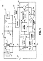
- Figure 1 is a block diagram illustrating an embodiment of a power supply including an embodiment of an adjustment circuit in a power supply regulator in accordance with the teachings of the present invention.
- Figure 2 is a diagram illustrating an embodiment of waveform of a switch current through a power switch in accordance with the teachings of the present invention.
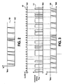
- Figure 3 is a diagram illustrating an embodiment of waveforms for a clock, a feedback signal and a switch current of a power supply regulator in accordance with the teachings of the present invention.
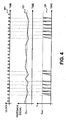
- Figure 4 is a diagram illustrating an embodiment of waveforms for a clock with distorted feedback signal and a resulting switch current of a power supply regulator as a consequence of missing adjustment circuitry in accordance with the teachings of the present invention.
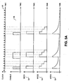
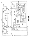
- Figure 5A shows diagrams illustrating embodiments of waveforms for a clock and feedback state events with various embodiments of modulation source waveforms of an embodiment of a power supply regulator in accordance with the teachings of the present invention.
- Figure 5B shows additional diagrams illustrating an embodiment of waveforms for a clock and feedback state events with various embodiments of modulation source waveforms of an embodiment of a power supply regulator in accordance with the teachings of the present invention.
- Figure 6A is a block diagram illustrating an embodiment of waveforms for another embodiment of a power supply including another embodiment of an adjustment circuit in a power supply regulator in accordance with the teachings of the present invention.
- Figure 6B shows embodiments of example waveforms of signals that use a modulation signal in accordance with the teachings of the present invention.
- Figure 7A is a block diagram illustrating an embodiment of a power supply regulator including an embodiment of an adjustment circuit in accordance with the teachings of the present invention.
- Figure 7B is a diagram that shows examples of waveforms that may be found in Figure 7A in accordance with the teachings of the present invention.
- Figure 8 is a block diagram illustrating another embodiment of a power supply regulator including another embodiment of an adjustment circuit in accordance with the teachings of the present invention.
- Figure 9 is a block diagram illustrating yet another embodiment of a power supply regulator including yet another embodiment of an adjustment circuit in accordance with the teachings of the present invention.
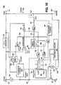
- Figure 10 is a block diagram illustrating still another embodiment of a power supply regulator including still another embodiment of an adjustment circuit in accordance with the teachings of the present invention.
- Embodiments of a power supply regulator that may be utilized in a power supply are disclosed.
- numerous specific details are set forth in order to provide a thorough understanding of the present invention. It will be apparent, however, to one having ordinary skill in the art that the specific detail need not be employed to practice the present invention. Well-known methods related to the implementation have not been described in detail in order to avoid obscuring the present invention.
- FIG. 1 is a block diagram illustrating an embodiment of a power supply 101 including an embodiment of an adjustment circuit 105 in a power supply regulator 103 in accordance with the teachings of the present invention.
- a voltage V IN 113 is coupled across an input of power supply 101 and is coupled to a primary winding 109 of an energy transfer element 107.
- a clamp 115 is coupled across primary winding 109 to clamp the voltage across primary winding 109.
- a first terminal 117 of power supply regulator 103 is coupled to energy transfer element 107 and a second terminal 119 is coupled to an input of power supply 101.
- a power switch 123 included in power supply regulator 103 is switched to couple or decouple the first terminal 117 from the second terminal 119 in response to a control signal 125, which is generated by a control circuit 135 of power supply regulator 103.
- the switching of power switch 123 regulates the transfer of energy from primary winding 109 to a secondary winding 111 of energy transfer element 107.
- diode 127 and capacitor 129 are coupled to secondary winding 111 at an output of power supply 101 such that a load 131 coupled to the output of power supply 101 is powered by receiving an output voltage V O and an output current I O .
- a feedback circuit 133 is coupled to the output of power supply 101 to generate a feedback signal 137, which is representative of an output level of power supply 101.
- the output level of power supply 101 may be a voltage, a current or a combination of both voltage and current.
- a third terminal 121 of power supply regulator 103 is coupled to receive feedback signal 137.
- power supply regulator 103 also includes one embodiment of a comparator 139 having an output 143 from which the results of a comparison between an input 141 and an input 145 are generated.
- input 141 is coupled to receive a threshold value U TH and input 145 is coupled to be responsive to feedback signal 137.
- the threshold value U TH is a turnoff threshold value.
- the output 143 of comparator 139 is a feedback state signal 124, which in one embodiment functions as a digital on/off signal or an enable signal to control circuit 135.
- the feedback state signal 124 at output 143 is a first state.
- the feedback state signal 124 at output 143 is a second state.
- one of the first and second states of the feedback state signal 124 is a logical high value and the other one of the first and second states of the feedback state signal 124 is a logical low value.
- the feedback state signal 124 is coupled to be received by control circuit 135, which helps to control the regulation of power supply 101.
- control circuit 135 also includes a current limit circuit, which is coupled to receive a current sense signal 147 from power switch 123.
- current sense signal 147 is representative of a current I D 126 through the power switch 123 and control circuit 135 also utilizes current sense signal 147 to help control the regulation of power supply 101.
- feedback signal 137 also indicates how much the output of power supply 101 is above or below a desired value by comparing the inputs 141 and 145 of comparator 139. If input 145 is less than the turnoff threshold U TH , then the feedback state 124 at output 143 of comparator 139 is a digital high value, and the control circuit 135 is allowed to operate the power switch 123. If input 145 is greater than the turnoff threshold U TH , then the feedback state 124 at output 143 of the comparator 139 is a digital low value, and the control circuit 135 is not permitted to close the power switch 123.
- control circuit 135 includes an oscillator that generates a clock signal 181 that defines the switching periods. The control circuit 135 determines whether or not the power switch 123 is allowed to close during a clock period. When the feedback state signal 124 received by control circuit 135 is a logical high value, the control circuit 135 is enabled to close power switch 123 at the beginning of a switching period. As summarized above, control circuit 135 senses the current I D 126 through power switch 123 with current sense signal 147. In one embodiment, the power switch 123 opens after either a maximum on-time, or when the power switch 123 current I D 126 reaches a maximum value I MAX .
- Figure 2 is a diagram illustrating an embodiment of typical waveform of the current I D 126 through power switch 123. In one embodiment, control circuit 135 regulates the output of power supply 101 by keeping the power switch 123 off during some switching periods.
- Figure 3 is a diagram illustrating an embodiment of waveforms for a clock signal 181, which is internal to the control circuit, the feedback signal 137 and the switch current I D 126 of a power supply regulator in accordance with the teachings of the present invention.
- feedback circuit 133 is assumed to have ideal characteristics such that modulation signal 128 is substantially zero.
- Figure 3 shows typical waveforms for the clock signal 181, the feedback signal 137, and the switch current I D 126 when the feedback circuit 133 has the ideal characteristics of high gain, high bandwidth, and no delay with the modulation signal 128 substantially zero.
- the power switch 123 operates in a pattern characterized by regular short intervals of clock periods where the power switch 123 is on, separated by intervals of clock periods where power switch 123 stays off. For any set of input and output conditions, there is a ratio between the number of clock periods when power switch 123 is on and the total number of clock periods that gives the desired regulated output for power supply 101.
- a desirable mode of operation is a repeating pattern of on and off clock periods that has a high fundamental frequency because the highest fundamental frequency gives the lowest magnitude of output ripple and reduces the likelihood of audio noise.
- Figure 4 is a diagram illustrating an embodiment of waveforms for a clock signal 181 with a non-ideal feedback circuit 137 resulting in a distorted feedback signal 137 and an undesirable pattern of switch current I D 126.
- the modulation signal 128 is assumed to be substantially zero.
- the switching of power switch 123 occurs in long intervals of clock cycles where the power switch 123 turns on, followed by long interval of clock cycles where the power switch 123 stays off.
- Such patterns of grouped pulses are undesirable because they can produce large output ripple and audio noise.
- the ON/OFF control of a switching regulator that uses non-ideal feedback circuits is improved in accordance with the teachings of the present invention.
- the principle employed by embodiments of the present invention is to temporarily modify the feedback signal or the threshold level with a non-zero modulation signal 128 as appropriate to which the feedback signal is compared to compensate for the distortion caused by low gain, low bandwidth, and delay. Knowledge of the timing and the expected characteristics of the feedback signal under ideal conditions make the compensation possible.
- adjustment circuit 105 includes a state machine 149 coupled to a modulation source 151.
- adjustment circuit 105 also includes an element 153, which is coupled to modulation source 151 and is coupled to receive the feedback signal 137 from the third terminal 121.
- element 153 is coupled to combine the modulation signal 128 that is output from modulation source 151 with the feedback signal 137 to input 145 of comparator 139. As a result, the feedback signal that is output from element 153 and is compared with the threshold level U TH at input 141 is adjusted with modulation signal 128 in accordance with the teachings of the present invention.
- the adjustment causes the difference between the high value and low value of the feedback signal to be approximately 80 per cent of the low value.
- the feedback state 124 signal at output 143 of comparator 139 which in one embodiment functions as the digital on/off signal or an enable signal to control circuit 135, is adjusted in accordance with the teachings of the present invention.
- the adjustment to the feedback state 124 signal tends to cause the feedback state 124 signal to revert from a state at the time of adjustment to a state immediately preceding the adjustment in accordance with the teachings of the present invention.
- state machine 149 in one embodiment is coupled to receive timing information from a clock signal 181 from control circuit 135.
- state machine 149 in one embodiment, is also coupled to receive information about the state of power supply 101 from the feedback state signal 124 generated at the output 143 of comparator 139. As shown, the state machine 149 causes the modulation signal 128 to be output from modulation source 151 to be added to the feedback signal 137 in accordance with the teachings of the present invention.
- Figure 5A gives examples of various embodiments of modulation signal 128, which are shown as MODULATION1, MODULATION2 and MODULATION3, with respect to the clock signal 181 from control circuit 135 and the feedback state signal 124 or enable events from output 143 in accordance with the teachings of the present invention.
- the modulation signal 128 from modulation source 151 provides the effect of artificially restoring information missing from the feedback signal 137. The result is an improvement in the pattern of switching cycles that increases the fundamental frequency of the sequence, reducing the magnitude of output ripple and lowering the likelihood of audio noise from power supply regulator 103 in accordance with the teachings of the present invention.
- the embodiment of modulation signal 128 shown as MODULATION1 is a fixed amplitude pulse that is produced in one embodiment when an embodiment of state machine 149 is implemented as a flip-flop.
- the digital stepped modulation of MODULATION2 results in another embodiment with state machine 149 and circuitry included in modulation source 151 to result in the digital stepped modulation in accordance with the teachings of the present invention.
- the smooth nonlinear ramp of MODULATION3 is an analog variant of MODULATION2 provided by another embodiment of state machine 149 and modulation source 151 in accordance with the teachings of the present invention.
- different modulation signals 128 may be selected in accordance with the deficiencies of the feedback circuit 133 and the desired performance of power supply regulator 103 in accordance with the teachings of the present invention.
- modulation signal 128 in Figure 5A are different from a conventional hysteresis signal modulation signal 128 that is illustrated in Figure 5B .
- the conventional hysteresis signal shown as HYSTERESIS1 modulation signal 128 in Figure 5B , changes between two values depending on the feedback state 124. Changes in the value of the hysteresis signal HYSTERESIS1 modulation signal 128 are synchronized with the clock that determines the beginning of a switching cycle.
- a feedback signal 137 cause a feedback state 124 to change from a previous state to a current state
- the initial effect of a HYSTERESIS1 modulation signal 128 is to maintain the current state.
- the current state will be maintained as long as the subsequent changes to the feedback signal are less than the value of the hysteresis signal. For example, when the feedback signal 137 decreases to cause the feedback state 124 to change from a low state to a high state, the summation of HYSTERESIS 1 modulation signal 128 with the feedback signal 137 would cause the feedback state 124 to remain in the high state when the feedback signal 137 increases by an amount less than the magnitude of the HYSTERESIS 1 modulation signal 128.
- variants of a conventional hysteresis signal may have more than one value or may change value with time, the initial effect of a hysteresis signal is to maintain the current state of a feedback state 124.
- a modulation signal is not limited to two values, and the value of a modulation signal is determined by more than just the current feedback state 137.
- the value of a modulation signal may be determined by the previous feedback state as well as the current feedback state.
- the value of a modulation signal may vary with time in a way that is unrelated to the current state or to the previous state.
- a fundamental distinction between a modulation signal and a conventional hysteresis signal is that the summation of a modulation signal 128 with a feedback signal 137 has the initial effect to alter the feedback state 124, whereas the summation of a HYSTERESIS 1 modulation signal 128 with a feedback signal 137 has the initial effect to maintain the feedback state 124.
- a modulation signal 128 would cause the feedback state 124 to revert to its former low state if the original decrease of feedback signal 137 was not sufficient to keep feedback state 124 in the high.
- the initial effect of a modulation signal is opposite to the initial effect of a hysteresis signal.
- FIG. 6A is a block diagram illustrating another embodiment of a power supply 601 including another embodiment of an adjustment circuit 605 in a power supply regulator 603 in accordance with the teachings of the present invention.
- the embodiment of power supply regulator 603 shares similarities with the embodiment of power supply regulator 103 of Figure 1 .
- a voltage V IN 613 is coupled across an input of power supply 601 and is coupled to a primary winding 609 of an energy transfer element 607.
- a clamp 615 is coupled across primary winding 609 to clamp the voltage across primary winding 609.
- a first terminal 617 of power supply regulator 603 is coupled to energy transfer element 607 and a second terminal 619 is coupled to an input of power supply 601.
- a power switch 623 of power supply regulator 603 is switched to couple or decouple the first terminal 617 from the second terminal 619 in response to a control signal 625, which is generated by a control circuit 635 of power supply regulator 603.
- the switching of power switch 623 regulates the transfer of energy from primary winding 609 to a secondary winding 611 of energy transfer element 607.
- diode 627 and capacitor 629 are coupled to secondary winding 611 at an output of power supply 601 such that a load 631 coupled to the output of power supply 601 is powered by receiving an output voltage V O and an output current I O .
- a feedback circuit 633 is coupled to the output power supply 601 to generate a feedback signal 637, which is representative of an output level of power supply 601.
- a third terminal 621 of power supply regulator 603 is coupled to receive feedback signal 637.
- power supply regulator 603 also includes one embodiment of a comparator 639 having an output 643 from which the results of a comparison between an input 641 and an input 645 are generated.
- a comparator 639 having an output 643 from which the results of a comparison between an input 641 and an input 645 are generated.
- One difference between the embodiments of power supply regulator 103 of Figure 1 and power supply regulator 603 of Figure 6A is with respect to the inputs to respective comparators 139 and 693.
- the output 143 of comparator 139 is responsive to the difference between the inputs 141 and 145, a subtraction of modulation from the threshold value U TH would have the same effect as addition of the same modulation to the feedback signal 137.
- input 645 is coupled to receive feedback signal 637 from third terminal 621, while input 641 is coupled to element 653, which is coupled to combine threshold level U TH with a modulation signal 628 from modulation source 651.
- element 653 is illustrated as subtracting a modulation signal 628 from U TH in accordance with the teachings of the present invention.
- the adjustment causes the difference between the high value and low value of U TH to be approximately 80 per cent of the low value.
- the output 643 of comparator 639 is a feedback state signal 624, which in one embodiment functions as a digital on/off signal or an enable signal to control circuit 635.
- control circuit 635 includes a current limit circuit, which is coupled to receive a current sense signal 647 from power switch 623.
- current sense signal 647 is representative of a current I D 626 through the power switch 623 and control circuit 635 also utilizes current sense signal 647 to help control the regulation of power supply 601.
- the operation and function of adjustment circuit 605 of Figure 6A is similar to the operation and function of adjustment circuit 105 of Figure 1 , with a difference being that that the threshold level U TH is adjusted instead of the feedback signal, as discussed.
- state machine 649 is coupled to receive clock signal 681 from control circuit 635 and feedback state signal 624 from the output 643 of comparator 639 to control the modulation signal 628 from modulation source 651.
- Various embodiments of the modulation signal 628 are illustrated as MODULATION1, MODULATION2 or MODULATION3 waveforms in Figure 5 , which may be produced by various embodiments of adjustment circuit modulation source 651 in accordance with the teachings of the present invention.
- Figure 6B shows waveforms of clock signal 681, signals 645 and 641 to the input of comparator 639, and switch current I D 626 for one embodiment that uses modulation signal 628 of the form illustrated in Figure 5A as MODULATION 1.
- the signals in Figure 6B illustrate how the introduction of a modulation signal 628 produces a desirable pattern of on and off switching cycles in response to a distorted feedback signal.
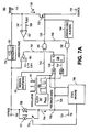
- FIG. 7A is a block diagram illustrating an embodiment of a power supply regulator 703 and Figure 7B is a diagram that shows examples of corresponding waveforms that may be found in Figure 7A in accordance with the teachings of the present invention.
- the power supply regulator includes a power switch 723 that is coupled between a drain terminal 717 and a source terminal 719.
- power switch 723 includes a metal oxide semiconductor field effect transistor (MOSFET). Power switch 723 is switched on and off according to control signal 725, which is received from AND gate 785.
- MOSFET metal oxide semiconductor field effect transistor
- the inputs to AND gate 785 include an output of latch 799, a bypass terminal 753 voltage indicator signal 765 provided by an undervoltage comparator 763, and a thermal status signal 783 from thermal shut down circuit 761.
- An oscillator 787 is included in power supply regulator 703 and generates a maximum duty cycle signal 789, which determines the maximum time that power switch 723 can couple drain terminal 717 and source terminal 719 in each cycle of operation.
- thermal shut down circuit 761 monitors the temperature of the power supply regulator 703 and provides the thermal status signal 783 as long as the temperature is below a threshold temperature.
- the threshold temperature is 135 degrees Celsius.
- the inputs to latch 799 include an OR gate 793 output signal 797 and an AND gate 791 output signal 795.
- the AND gate 791 output signal 795 is provided when no current is provided to feedback terminal 721.
- AND gate 791 provides output when an active feedback state signal 724 or enable signal is received from node 743 and oscillator 787 provides an active clock signal 781.
- current source 759 will pull the feedback state signal 724 or enable signal to a logic high state when the current provided to feedback terminal 721 is less than the current source 759 current. In one embodiment, the current source 759 current is 50 microamperes.
- the clock signal 781 is transferred to latch 799 by the AND gate 791, thereby setting the latch 799 and enabling that cycle to go through and turn on the power switch 723.
- the feedback state signal 724 or enable signal from node 743 is low, it blocks the clock signal 781 from setting the latch 799, and keeps the power switch 723 off during that cycle.
- the AND gate 791 output signal 795 is an oscillating signal having a frequency of substantially zero.
- the AND gate 791 1 output signal 795 is an oscillating signal having a substantially non-zero frequency.
- a current sense signal 747 is coupled to sense a current I D 726 through power switch 723.
- a current limit threshold comparator 767 is coupled to receive the current sense signal 747 and compare it with a V LIMIT 769 value. When the current I D 726 through power switch 723 is greater than a current limit, the voltage across power switch 723, as sensed with current sense signal 747, will be greater than V LIMIT 769 and an active current limit signal 706 is output by comparator 767.
- AND gate 702 is coupled to receive the current limit signal 706 and a signal from leading edge blanking circuit 704. In one embodiment, leading edge blanking circuit 704 disables OR gate 793 from sensing a current limit condition during a short time after power switch 723 turns on.
- OR gate 793 In operation, the output of AND gate 702 is received by OR gate 793 when the current threshold limit signal 706 is reached or during the time when maximum duty cycle signal 789 is in an off state.
- OR gate 793 output signal 797 will be provided when the maximum duty cycle signal 789 is off or when the current limit is sensed by current sense 747 is reached in order to turn off the power switch 723.
- power switch 723 is held off during the next switching cycle when the current provided by feedback terminal 721 pulls the enable signal at node 743, which is the feedback state signal 724, low to create a condition where there will be no additional power supplied to the load.
- the feedback state signal 724 which is the enable signal at node 743, is high due to the operation of current source 759, and power switch 723 will resume operation upon the beginning of the next on-period of the maximum duty cycle signal 789.
- a regulator circuit 755, which includes a current source 757 functions as a bypass charge circuit and regulates the voltage level which in one embodiment is five point seven (5.7) volts of a capacitor externally coupled to bypass terminal 753. This is done in one embodiment by charging the capacitor externally coupled to bypass terminal 753 when power switch 723 is not conducting. Undervoltage circuit 763 prevents the power switch 723 from conducting again until the voltage at bypass terminal 753 reaches the desired voltage level.
- the feedback state signal 724 or enable signal on node 743 is adjusted in accordance with the teachings of the present invention by switchably coupling current source 751 to node 743 through switch 753 in response to state machine 749.
- current source 751 may be considered to be a modulation source and switch 753 may be considered to be an element to switchably combine the feedback signal with the modulation source in response to state machine 749 in accordance with the teachings of the present invention.
- current source 751 is switched in parallel with current source 759 to change the current provided to node 743.
- the current source 751 current is 40 microamperes and the current source 759 current is 50 microamperes.
- state machine 749 receives the feedback state signal 724 or enable signal from node 743 and the clock signal 781.
- state machine 749 includes logic that in one embodiment is a flip-flop.
- the value of the feedback current that determines whether the feedback state signal 724 or enable signal from node 743 is high or low is modulated by the current from current source 751.
- the feedback current is modulated by a pulse.
- the current is modulated by a ramp.
- a plurality of current sources may be switched in parallel with current source 759, individually responsive to state machine 749 to modulate the current provided to the feedback terminal 721 in accordance with the teachings of the present invention.
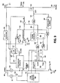
- FIG 8 is a block diagram illustrating another embodiment of a power supply regulator 803 in accordance with the teachings of the present invention.
- power supply regulator 803 of Figure 8 is similar to power supply regulator 703 of Figure 7 .
- power supply regulator 803 is functionally equivalent to power supply regulator 703 and share a number of common elements.
- a difference between power supply regulator 803 and power supply regulator 703 is that current source 851 is switchably coupled through switch 853 to remove current from node 743 or feedback terminal 721 to adjust the feedback state signal 724 or enable signal from node 743 in response to state machine 849 as shown.
- current source 759 current is 90 microamperes and current source current 851 is 40 microamperes.
- the embodiment shown in Figure 8 shows current source 851 coupled to node 743 and the feedback terminal 721 and switched in response to a state machine 849.
- State machine 849 receives the feedback state signal 724 or enable signal from node 743 and clock signal 781.
- state machine 849 includes logic that in one embodiment is a flip-flop.
- current source 851 has a constant value such that a current pulse is subtracted from the feedback terminal 721 in response to state machine 849.
- current source 851 increases or decreases with time such that a ramp is subtracted from the feedback terminal 721 in response to state machine 849.
- a plurality of current sources may be switched individually in response to a state machine 849 to add or remove current from the feedback terminal 721, modulating the current that determines whether the feedback state signal 724 or enable signal from node 743 is high or low in accordance with the teachings of the present invention.
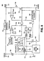
- FIG. 9 is a block diagram illustrating yet another embodiment of a power supply regulator 903 in accordance with the teachings of the present invention.
- switching regulator circuit 903 includes a power switch 923, which in one embodiment includes a MOSFET that is coupled between a drain terminal 917 and a source terminal 919.
- Power switch 923 is switched on and off according to a control signal 925 generated by the control circuit.
- control signal 925 is input into the gate of power switch 923 by AND gate 985.
- the control circuit includes AND gates 991 and 985, OR gate 993, latch 999, oscillator 987, state machine circuitry 910, current limit adjust circuitry 912 and their associated elements.
- the input of AND gate 985 includes an output of a latch 999, a bypass terminal 953 voltage indicator 965 provided by undervoltage comparator 963, and a thermal status signal 983 from thermal shut-down circuit 961.
- maximum duty cycle signal 989 generated by oscillator 987 determines the maximum time that power switch 923 can conduct in each cycle of operation.
- the feedback state signal 924 or enable signal from node 943 When the current being pulled out of the feedback terminal 921 is greater than an enable threshold current provided by current source 959, the feedback state signal 924 or enable signal from node 943 will be pulled to a low state. When the current being pulled out of the feedback terminal 921 is less than the enable threshold current provided by current source 959, the feedback state signal 924 or enable signal from node 943 will be pulled to a high state. As shown, the feedback state signal 924 or enable signal from node 943 is also coupled to be received by the state machine circuitry 910. State machine circuitry 910 will send signals 914 to the current limit (Ilim) adjust circuitry 912, setting the current limit of I DRAIN 916 through power switch 923 to be lower at light load or higher at high load. In one embodiment, there are three signals 914A, 914B and 914C included in signals 914.
- current limit adjust circuitry 912 adjusts the current limit in digital steps. Transitions to a higher current limit state occur after a pattern ofN consecutive feedback state signal 924 or enable signal logic highs from node 943. Transitions to a lower current limit state occur after a pattern of N consecutive feedback state signal 924 or enable signal logic lows from node 943. In one embodiment, N equals 6.
- the inputs to latch 999 include an OR gate 993 output signal 997 and an AND gate 991 output signal 995.
- the AND gate 991 output signal 995 is high only when feedback state 924 and clock signal 981 generated by oscillator 987 are both high.
- AND gate 991 provides output when logical high signal 943 is received and clock signal 981 is provided by oscillator 987.
- the clock signal 981 is transferred to latch 999 by the AND gate 991, thereby setting the latch 999 and enabling that cycle to go through and turn on the power switch 923.
- the signal 943 is low, it blocks the clock signal 981 from setting the latch 999, and keeps the power switch 923 off during that cycle.
- OR gate 993 output signal 997 is provided when the current threshold limit is reached as indicated by signal 906 or during the time when maximum duty cycle signal 989 is in an off state. In operation, OR gate 993 output signal 997 is high when either the maximum duty cycle signal 989 is low or when the current limit is reached as indicated with signal 906 after the leading edge blanking delay, which is determined by leading edge blanking circuit 904 through AND gate 902, in order to turn off the power switch 923.
- signal 947 generated by current limit adjust circuitry 912 is a voltage level proportional to the voltage across the power switch 923.
- Current limit states are determined by signals 914A, 914B and 914C, which are generated by state machine circuitry 910. At higher current limit states, current limit adjust circuitry 912 changes signal 947 to become a lower proportion of the voltage across power switch 923. At lower current limit states, current limit adjustment circuitry 912 causes signal 947 to become a higher proportion of the voltage across power switch 923.
- Current threshold comparator 967 then compares current threshold limit voltage V ILIMIT 969 to the set voltage signal 947. If the current threshold limit voltage V ILIMIT 969 is above signal 947, the current limit signal is triggered, and the power switch 923 is turned offuntil the beginning of the next on-time.
- the switching regulator circuit 903 turns off the power switch 923 after the current on cycle when the signal 943 is pulled low and creates a condition where there will be no additional power supplied to the load. Accordingly, signal 943 in response to the output of the power supply selectively allows the on time of a current cycle of control signal 925 to be maintained and not allow or disable an on time of a next cycle of control signal 925. When signal 943 is pulled high, the power switch 923 will resume operation upon the beginning of the next on-period of the maximum duty cycle signal 989.
- a bypass charge circuit or 5.7 V regulator 955 which includes the current source from the drain terminal 917 to the bypass terminal 953, regulates the power level of capacitor externally coupled to bypass terminal 953 at a voltage level, which in one embodiment is 5.7 volts. This is done by charging the capacitor that is externally coupled to bypass terminal 953 while the power switch 923 is not conducting.
- undervoltage comparator 963 prevents the power switch 923 from conducting again until the voltage at bypass terminal 953 reaches the desired voltage level.
- Inverter 922 inverts the output of an undervoltage comparator 963.
- the feedback state signal 924 or enable signal from node 943 is adjusted in accordance with the teachings of the present invention by switchably coupling current source 951 to node 943 through switch 953 in response to state machine 949.
- current source 951 may be considered to be a modulation source and switch 953 may be considered to be an element to switchably combine the feedback signal from feedback terminal 921 with the modulation source in response to state machine 949 in accordance with the teachings of the present invention.
- current source 951 is switched in parallel with current source 959 to change the current provided to node 943.
- current source 959 current is 50 microamperes and current source 951 current is 40 microamperes.
- state machine 949 receives the feedback state signal 924 or enable signal from node 943 and the clock signal 981.
- state machine 949 includes logic that in one embodiment includes a flip-flop.
- the value of the feedback current that determines whether the feedback state signal 924 or enable signal from node 943 is high or low is modulated by the current from current source 951.
- the feedback current is modulated by a pulse.
- the current is modulated by a ramp.
- a plurality of current sources may be switched in parallel with current source 959, individually responsive to state machine 949 to modulate the current provided to the feedback terminal 921 in accordance with the teachings of the present invention.
- FIG 10 is a block diagram illustrating still another embodiment of a power supply regulator in accordance with the teachings of the present invention.
- power supply regulator 1003 of Figure10 is similar to power supply regulator 903 of Figure 9 .
- power supply regulator 1003 is functionally equivalent to power supply regulator 903 and shares a number of common elements.
- a difference between power supply regulator 1003 and power supply regulator 903 is that current source 1051 is switchably coupled through switch 1053 to remove current from node 943 or feedback terminal 921 to adjust the feedback state signal 924 or enable signal from node 943 in response to state machine 1049 as shown.
- current source 959 current is 90 microamperes and current source 1051 current is 40 microamperes.
- the embodiment shown in Figure 10 shows current source 1051 coupled to node 943 and switched to source terminal 919 in response to a state machine 1049.
- State machine 1049 receives the feedback state signal 924 or enable signal from node 943 and clock signal 981.
- state machine 1049 includes logic that in one embodiment includes a flip-flop.
- current source 1051 has a constant value such that a current pulse is subtracted from the feedback terminal 921 in response to state machine 1049.
- current source 1051 increases or decreases with time such that a ramp is subtracted from the feedback terminal 921 in response to state machine 1049.
- a plurality of current sources may be switched individually in response to a state machine 1049 to add or remove current from the feedback terminal 921, modulating the current that determines whether the feedback state signal 924 or enable signal from node 943 is high or low in accordance with the teachings of the present invention.
Landscapes
- Engineering & Computer Science (AREA)
- Power Engineering (AREA)
- Dc-Dc Converters (AREA)
Applications Claiming Priority (1)
| Application Number | Priority Date | Filing Date | Title |
|---|---|---|---|
| US11/213,296 US7233504B2 (en) | 2005-08-26 | 2005-08-26 | Method and apparatus for digital control of a switching regulator |
Publications (3)
| Publication Number | Publication Date |
|---|---|
| EP1758236A2 EP1758236A2 (en) | 2007-02-28 |
| EP1758236A3 EP1758236A3 (en) | 2009-03-04 |
| EP1758236B1 true EP1758236B1 (en) | 2011-12-21 |
Family
ID=37499305
Family Applications (1)
| Application Number | Title | Priority Date | Filing Date |
|---|---|---|---|
| EP06253525A Not-in-force EP1758236B1 (en) | 2005-08-26 | 2006-07-05 | Method and apparatus for digital control of a switching regulator |
Country Status (5)
| Country | Link |
|---|---|
| US (7) | US7233504B2 (enExample) |
| EP (1) | EP1758236B1 (enExample) |
| JP (1) | JP5242898B2 (enExample) |
| CN (2) | CN103762847B (enExample) |
| AT (1) | ATE538528T1 (enExample) |
Families Citing this family (50)
| Publication number | Priority date | Publication date | Assignee | Title |
|---|---|---|---|---|
| US6876181B1 (en) | 1998-02-27 | 2005-04-05 | Power Integrations, Inc. | Off-line converter with digital control |
| US9495381B2 (en) | 2005-01-12 | 2016-11-15 | Wandisco, Inc. | Geographically-distributed file system using coordinated namespace replication over a wide area network |
| US8364633B2 (en) | 2005-01-12 | 2013-01-29 | Wandisco, Inc. | Distributed computing systems and system components thereof |
| US9332069B2 (en) | 2012-12-28 | 2016-05-03 | Wandisco, Inc. | Methods, devices and systems for initiating, forming and joining memberships in distributed computing systems |
| US9424272B2 (en) | 2005-01-12 | 2016-08-23 | Wandisco, Inc. | Distributed file system using consensus nodes |
| US7233504B2 (en) | 2005-08-26 | 2007-06-19 | Power Integration, Inc. | Method and apparatus for digital control of a switching regulator |
| KR101247801B1 (ko) * | 2005-10-25 | 2013-03-26 | 페어차일드코리아반도체 주식회사 | 스위칭 모드 파워 서플라이 |
| US7518350B2 (en) * | 2005-12-16 | 2009-04-14 | Silicon Laboratories Inc. | MCU/driver point of load digital controller with optimized voltage |
| US7342365B2 (en) * | 2006-02-09 | 2008-03-11 | Linear Technology Corp. | Systems and methods for reducing input current in photoflash chargers |
| US7518885B2 (en) | 2006-10-04 | 2009-04-14 | Power Integrations, Inc. | Method and apparatus for a control circuit with multiple operation modes |
| US7502236B2 (en) | 2006-10-04 | 2009-03-10 | Power Integrations, Inc. | Power supply controller responsive to a feedforward signal |
| US7576528B2 (en) | 2006-10-04 | 2009-08-18 | Power Integrations, Inc. | Control circuit responsive to an impedance |
| US7764520B2 (en) * | 2007-04-06 | 2010-07-27 | Power Integrations, Inc. | Method and apparatus for on/off control of a power converter |
| KR101284827B1 (ko) | 2007-05-21 | 2013-07-10 | 페어차일드코리아반도체 주식회사 | 스위치 제어 장치, 스위치 제어 방법 및 이를 이용하는컨버터 |
| US7696737B2 (en) * | 2007-12-21 | 2010-04-13 | Power Intergrations, Inc. | Method and apparatus to control a power supply for high efficiency |
| JP2010022097A (ja) * | 2008-07-09 | 2010-01-28 | Panasonic Corp | スイッチング制御回路、半導体装置、およびスイッチング電源装置 |
| US8159843B2 (en) * | 2009-01-30 | 2012-04-17 | Power Integrations, Inc. | Method and apparatus to regulate an output voltage of a power converter at light/no load conditions |
| US8098506B2 (en) | 2009-06-02 | 2012-01-17 | Power Integrations, Inc. | Single-stage power supply with power factor correction and constant current output |
| CN101645656B (zh) * | 2009-09-01 | 2011-09-14 | 成都芯源系统有限公司 | 电流峰值压缩方法及采用该方法的控制电路 |
| US8564256B2 (en) * | 2009-11-18 | 2013-10-22 | Silicon Laboratories, Inc. | Circuit devices and methods of providing a regulated power supply |
| US8242766B2 (en) | 2010-04-20 | 2012-08-14 | Power Integrations, Inc. | Dimming control for a switching power supply |
| ITMI20110546A1 (it) * | 2011-04-04 | 2012-10-05 | St Microelectronics Srl | Dispositivo di controllo della frequenza di commutazione di un converter quasi risonante e relativo metodo di controllo. |
| US8797766B2 (en) * | 2011-04-06 | 2014-08-05 | Bose Corporation | Power supply with tickle pulse injection |
| JP2013055620A (ja) * | 2011-09-06 | 2013-03-21 | Hitachi Automotive Systems Ltd | 電流制御装置 |
| US8823353B2 (en) | 2011-10-20 | 2014-09-02 | Power Integrations, Inc. | Power controller with smooth transition to pulse skipping |
| US9048747B2 (en) | 2011-11-23 | 2015-06-02 | Zahid Ansari | Switched-mode power supply startup circuit, method, and system incorporating same |
| JP6015281B2 (ja) * | 2012-09-20 | 2016-10-26 | 富士電機株式会社 | スイッチング電源装置 |
| US9363856B2 (en) | 2012-10-25 | 2016-06-07 | Koninklijke Philips N.V. | Driver device and driving method for driving a load, in particular an LED unit |
| US9264516B2 (en) * | 2012-12-28 | 2016-02-16 | Wandisco, Inc. | Methods, devices and systems enabling a secure and authorized induction of a node into a group of nodes in a distributed computing environment |
| US9246392B2 (en) | 2013-03-13 | 2016-01-26 | Power Integrations, Inc. | Switched mode power converter controller with ramp time modulation |
| US9009215B2 (en) | 2013-03-15 | 2015-04-14 | Wandisco, Inc. | Methods, devices and systems for dynamically managing memberships in replicated state machines within a distributed computing environment |
| CN106664032B (zh) | 2014-08-08 | 2019-12-03 | 飞利浦照明控股有限公司 | 具有控制回路的转换器 |
| US9680383B2 (en) * | 2014-11-07 | 2017-06-13 | Power Integrations, Inc. | Input overvoltage protection using current limit |
| US9774248B2 (en) * | 2014-11-10 | 2017-09-26 | Power Integrations, Inc. | Introducing jitter to a switching frequency by way of modulating current limit |
| US9450478B1 (en) * | 2015-04-10 | 2016-09-20 | Power Integrations, Inc. | Load responsive jitter |
| US9584033B1 (en) * | 2015-10-19 | 2017-02-28 | Chicony Power Technology Co., Ltd. | Power supply device for varying an output voltage |
| CN105322803B (zh) * | 2015-11-02 | 2018-03-06 | 深圳创维-Rgb电子有限公司 | 恒压恒流同步输出电源及电视机 |
| US9876433B2 (en) * | 2016-02-26 | 2018-01-23 | Power Integrations, Inc. | Reduction of audible noise in a power converter |
| US9893630B2 (en) | 2016-02-26 | 2018-02-13 | Power Integrations, Inc. | Reduction of audible noise in a power converter |
| US10243442B1 (en) | 2017-11-22 | 2019-03-26 | Power Integrations, Inc. | Controller with frequency to on-time converter |
| CN109995220B (zh) * | 2017-12-29 | 2020-10-20 | 东南大学 | 一种提高反激式谐振开关电源ccm模式转换效率的方法 |
| US11128224B2 (en) * | 2018-07-30 | 2021-09-21 | Texas Instruments Incorporated | Methods and apparatus for adaptive synchronous rectifier control |
| US10418908B1 (en) * | 2018-10-16 | 2019-09-17 | Power Integrations, Inc. | Controller with variable sampling generator |
| US10389226B1 (en) * | 2018-10-23 | 2019-08-20 | Power Integrations, Inc. | Controller with ripple compensation |
| CN111987907A (zh) * | 2019-05-24 | 2020-11-24 | 德克萨斯仪器股份有限公司 | 一种开关模式电源电路 |
| US11356010B2 (en) | 2020-05-11 | 2022-06-07 | Power Integrations, Inc. | Controller with frequency request circuit |
| US11923779B2 (en) * | 2020-11-05 | 2024-03-05 | Astec International Limited | Control circuits and methods for regulating output voltages |
| KR20220169774A (ko) * | 2021-06-21 | 2022-12-28 | 휴렛-팩커드 디벨롭먼트 컴퍼니, 엘.피. | 화성 형성 장치의 변환기 출력 스위치 실패모드시 보호장치 |
| WO2023277922A1 (en) | 2021-07-02 | 2023-01-05 | Power Integrations, Inc. | Adaptive ramp time modulation |
| CN113517810B (zh) * | 2021-07-23 | 2023-02-03 | 昂宝电子(上海)有限公司 | 开关变换器控制系统和方法 |
Family Cites Families (163)
| Publication number | Priority date | Publication date | Assignee | Title |
|---|---|---|---|---|
| US355399A (en) * | 1887-01-04 | Roller-skate wheel | ||
| US1378585A (en) * | 1917-08-14 | 1921-05-17 | Curnutt Elmer | Telephone system |
| US3491252A (en) | 1964-11-16 | 1970-01-20 | United Systems Corp | Ac-dc converter |
| US3555399A (en) | 1967-11-16 | 1971-01-12 | Gen Systems Inc | Commutation systems incorporating the energy logic concept |
| US3629622A (en) | 1970-04-03 | 1971-12-21 | Sylvania Electric Prod | Switching regulator having a low dissipation current overload detection device |
| US3840797A (en) | 1970-12-28 | 1974-10-08 | Us Navy | Related power supply |
| US4151387A (en) * | 1971-04-06 | 1979-04-24 | Environment/One Corporation | Metal base cookware induction heating apparatus having improved power control circuit for insuring safe operation |
| US3916224A (en) | 1973-08-02 | 1975-10-28 | Ibm | Transistor switching regulator control utilizing charging of bootstrap circuit to provide ramp-up |
| JPS51107826A (enExample) | 1975-03-19 | 1976-09-24 | Fuji Photo Film Co Ltd | |
| US3978393A (en) | 1975-04-21 | 1976-08-31 | Burroughs Corporation | High efficiency switching regulator |
| US4058758A (en) | 1976-07-02 | 1977-11-15 | Bell Telephone Laboratories, Incorporated | Cooperative primary and secondary current limiting to selectively limit aggregate and individual current outputs of a multi output converter |
| US4143282A (en) | 1976-12-03 | 1979-03-06 | Rca Corporation | Bilateral energy transfer apparatus |
| US4236198A (en) | 1977-12-16 | 1980-11-25 | Sony Corporation | Switching regulator |
| FR2413710A1 (fr) | 1977-12-29 | 1979-07-27 | Thomson Csf | Circuit de commande de puissance et alimentation a decoupage l'utilisant |
| DE3007566A1 (de) | 1980-02-28 | 1981-09-03 | Siemens AG, 1000 Berlin und 8000 München | Freischwingender sperrwandler |
| GB2075786B (en) | 1980-03-21 | 1984-07-11 | Electrotech Instr Ltd | Switch mode converters |
| US4400767A (en) | 1981-06-30 | 1983-08-23 | Honeywell Information Systems Inc. | Self start flyback power supply |
| GB2116787A (en) | 1981-09-16 | 1983-09-28 | Gould Inc | Efficient current modulator useful with inductive loads |
| JPS5848009U (ja) * | 1981-09-21 | 1983-03-31 | クラリオン株式会社 | 車載用テ−ププレ−ヤの防水構造 |
| US4481564A (en) | 1982-09-09 | 1984-11-06 | Zenith Electronics Corporation | Switched-mode power supply |
| US4559590A (en) | 1983-03-24 | 1985-12-17 | Varian Associates, Inc. | Regulated DC to DC converter |
| US4495554A (en) | 1983-03-28 | 1985-01-22 | International Business Machines Corporation | Isolated power supply feedback |
| JPS59201675A (ja) | 1983-04-25 | 1984-11-15 | エヌ・シ−・ア−ル・コ−ポレ−シヨン | 直流安定化電源用発振周波数安定化方法 |
| US4695742A (en) | 1983-05-09 | 1987-09-22 | Sangamo Weston, Inc. | Charge balance voltage-to-frequency converter utilizing CMOS circuitry |
| JPS6017240U (ja) | 1983-07-11 | 1985-02-05 | 出光石油化学株式会社 | 液体試料用容器 |
| US4533986A (en) | 1983-10-31 | 1985-08-06 | General Electric Company | Compact electrical power supply for signal processing applications |
| US4622627A (en) | 1984-02-16 | 1986-11-11 | Theta-J Corporation | Switching electrical power supply utilizing miniature inductors integrally in a PCB |
| US4791544A (en) | 1984-09-21 | 1988-12-13 | Veeco Instruments | Regulating control for single-ended switching power supply |
| US4739462A (en) | 1984-12-26 | 1988-04-19 | Hughes Aircraft Company | Power supply with noise immune current sensing |
| IT1215279B (it) | 1985-06-10 | 1990-01-31 | Ates Componenti Elettron | Dispositivo elettrico di potenza intelligente a circuito integrato monolitico. |
| DE3524767A1 (de) | 1985-07-11 | 1987-01-22 | Philips Patentverwaltung | Getakteter gleichspannungswandler |
| US4800323A (en) | 1985-11-04 | 1989-01-24 | Tomar Electronics, Inc. | Single-ended self-oscillating dc-dc converter for intermittently energized load having VBE responsive current limit circuit |
| US4706177A (en) | 1985-11-14 | 1987-11-10 | Elliot Josephson | DC-AC inverter with overload driving capability |
| US4761544A (en) * | 1985-11-15 | 1988-08-02 | Hewlett-Packard Company | Means and method of scaling time interval measurements from an optical bar code scanner to improve decoder efficiency |
| US4887199A (en) | 1986-02-07 | 1989-12-12 | Astec International Limited | Start circuit for generation of pulse width modulated switching pulses for switch mode power supplies |
| US4695936A (en) | 1986-02-07 | 1987-09-22 | Astec Components, Ltd. | Switching mode power supply start circuit |
| DE3610253A1 (de) | 1986-03-26 | 1987-10-08 | Sgs Halbleiterbauelemente Gmbh | Steuerschaltung fuer einen kommutatorlosen gleichstrommotor |
| JPH0322862Y2 (enExample) | 1986-03-31 | 1991-05-17 | ||
| IT1190632B (it) | 1986-04-22 | 1988-02-16 | Sgs Microelettronica Spa | Limitatore di corrente a corrente costante per dispositivi di pilotaggio a commutazione |
| US4737898A (en) | 1987-02-13 | 1988-04-12 | Northern Telecom Limited | Single-ended self-oscillating, DC-DC converter with regulation and inhibit control |
| US4734839A (en) | 1987-03-23 | 1988-03-29 | Barthold Fred O | Source volt-ampere/load volt-ampere differential converter |
| IT1215463B (it) | 1987-05-07 | 1990-02-14 | Sgs Microelettronica Spa | Generatore di impulsi di riposizionamento in coincidenza colla salita dell'alimentazione, per circuiti integrati di tipo cmos. |
| US4862339A (en) | 1987-06-05 | 1989-08-29 | Yokogawa Electric Corporation | DC power supply with improved output stabilizing feedback |
| US4761724A (en) | 1987-06-29 | 1988-08-02 | The United States As Represented By The United States Department Of Energy | Transformer coupling for transmitting direct current through a barrier |
| KR910002377B1 (ko) | 1987-09-18 | 1991-04-20 | 가부시기가이샤 하다찌세이사구쇼 | 스위칭전원 |
| US4809148A (en) | 1987-10-21 | 1989-02-28 | British Columbia Telephone Company | Full-fluxed, single-ended DC converter |
| JPH01117656A (ja) | 1987-10-29 | 1989-05-10 | Fanuc Ltd | スイッチングレギュレータ |
| US4811184A (en) | 1988-05-10 | 1989-03-07 | General Electric Company | Switch-mode power supply with dynamic adjustment of current sense magnitude |
| JPH01311863A (ja) | 1988-06-09 | 1989-12-15 | Fanuc Ltd | 電圧低下検出回路 |
| US4806844A (en) | 1988-06-17 | 1989-02-21 | General Electric Company | Circuit for providing on-chip DC power supply in an integrated circuit |
| US4943761A (en) * | 1988-07-06 | 1990-07-24 | Westinghouse Electric Corp. | Current limited DC power controller |
| DE58908719D1 (de) | 1988-07-27 | 1995-01-19 | Siemens Ag | Schaltungsanordnung zum Erfassen des Kurzschlusses einer mit einem FET in Reihe liegenden Last. |
| US4928220A (en) | 1988-10-14 | 1990-05-22 | Compaq Computer Inc. | Switching mode DC-to-DC power supply with improved current sensing |
| US4870555A (en) | 1988-10-14 | 1989-09-26 | Compaq Computer Corporation | High-efficiency DC-to-DC power supply with synchronous rectification |
| US4858094A (en) | 1988-10-18 | 1989-08-15 | Allied-Signal Inc. | Switched mode power supply with improved load regulation |
| US4890210A (en) | 1988-11-15 | 1989-12-26 | Gilbarco, Inc. | Power supply having combined forward converter and flyback action for high efficiency conversion from low to high voltage |
| JPH02159975A (ja) | 1988-12-09 | 1990-06-20 | Murata Mfg Co Ltd | 自励発振型コンバータ |
| JPH07118918B2 (ja) | 1989-01-26 | 1995-12-18 | 三菱電機株式会社 | Dc/dc電源装置 |
| NL8900508A (nl) | 1989-03-02 | 1990-10-01 | Philips Nv | Geschakelde voedingsspanningsschakeling met aanloopschakeling. |
| US4941078A (en) | 1989-03-07 | 1990-07-10 | Rca Licensing Corporation | Synchronized switch-mode power supply |
| US4943903A (en) | 1989-03-14 | 1990-07-24 | Cardwell Jr Gilbert I | Power supply in which regulation is achieved by processing a small portion of applied power through a switching regulator |
| JP2880187B2 (ja) | 1989-07-19 | 1999-04-05 | 株式会社日立製作所 | デジタルテレビジョン受像機 |
| JP2686135B2 (ja) | 1989-03-28 | 1997-12-08 | 松下電工株式会社 | 定電流電源回路 |
| JPH02262868A (ja) | 1989-03-31 | 1990-10-25 | Ricoh Co Ltd | 定電圧出力回路 |
| JPH0322862A (ja) | 1989-06-20 | 1991-01-31 | Matsushita Electric Ind Co Ltd | スイッチングレギュレータ装置 |
| CA2019525C (en) | 1989-06-23 | 1995-07-11 | Takuya Ishii | Switching power supply device |
| DE3930432A1 (de) | 1989-09-12 | 1991-05-16 | Siemens Ag | Schaltnetzteil |
| DE58907009D1 (de) | 1989-09-29 | 1994-03-24 | Siemens Ag | Schaltungsanordnung für ein Sperrwandler-Schalnetzteil. |
| US5013998A (en) | 1989-12-18 | 1991-05-07 | Varga Ljubomir D | Synthesis of zero-impedance converter |
| US5012401A (en) | 1990-03-19 | 1991-04-30 | Allied-Signal Inc. | Switching power supply with foldback current limiting |
| US5289101A (en) | 1990-04-27 | 1994-02-22 | Fuji Electric Co., Ltd. | Battery charger with charging current controller |
| US5014178A (en) | 1990-05-14 | 1991-05-07 | Power Integrations, Inc. | Self powering technique for integrated switched mode power supply |
| US5018058A (en) * | 1990-07-05 | 1991-05-21 | Power Management International, Inc. | High frequency AC voltage control |
| JP2806002B2 (ja) | 1990-07-31 | 1998-09-30 | ヤマハ株式会社 | スイッチング電源装置 |
| US5297014A (en) | 1991-01-09 | 1994-03-22 | Canon Kabushiki Kaisha | Switching DC power supply apparatus |
| JPH04120118U (ja) | 1991-04-03 | 1992-10-27 | スタンレー電気株式会社 | スイツチングレギユレータ |
| DE4111277A1 (de) | 1991-04-08 | 1992-10-15 | Thomson Brandt Gmbh | Anlaufschaltung fuer ein schaltnetzteil |
| US5309078A (en) * | 1991-07-11 | 1994-05-03 | Sgs-Thomson Microelectronics, Inc. | Synchronous rectification method for reducing power dissipation in motor drivers in PWM mode |
| US5177408A (en) | 1991-07-19 | 1993-01-05 | Magnetek Triad | Startup circuit for electronic ballasts for instant-start lamps |
| US5161098A (en) | 1991-09-09 | 1992-11-03 | Power Integrations, Inc. | High frequency switched mode converter |
| US5394017A (en) | 1991-11-05 | 1995-02-28 | Alliedsignal Inc. | Circuit for sustaining output power during input power interruption |
| US5457621A (en) | 1992-02-21 | 1995-10-10 | Abb Power T&D Company Inc. | Switching power supply having voltage blocking clamp |
| US5260861A (en) | 1992-05-01 | 1993-11-09 | Wert Harry E | Digital controlled converter and method |
| US5333104A (en) | 1992-05-22 | 1994-07-26 | Matsushita Electric Works, Ltd. | Inverter power source |
| US5302889A (en) | 1992-06-19 | 1994-04-12 | Honeywell Inc. | Voltage regulator |
| US5619403A (en) | 1992-07-24 | 1997-04-08 | Canon Kabushiki Kaisha | Multi-output power supply apparatus |
| US5313381A (en) | 1992-09-01 | 1994-05-17 | Power Integrations, Inc. | Three-terminal switched mode power supply integrated circuit |
| FR2696062B1 (fr) | 1992-09-23 | 1994-12-09 | Sgs Thomson Microelectronics | Commutateur électrique de puissance commandé et procédé de commutation d'un circuit électrique de puissance. |
| EP0590220B1 (en) | 1992-09-28 | 1996-06-05 | STMicroelectronics S.r.l. | Highly reliable, low dissipation boost circuit |
| US5408173A (en) | 1992-10-01 | 1995-04-18 | Kronos Incorporated | Manual-adjustment-free controlled-voltage and current-limited D.C. voltage supply |
| JP3366058B2 (ja) * | 1992-10-07 | 2003-01-14 | 浩 坂本 | 電源装置 |
| US5321349A (en) * | 1992-12-08 | 1994-06-14 | Iwei Technology Co., Ltd. | Rechargeable/portable multi-voltage dc power supply |
| US5434768A (en) * | 1993-02-12 | 1995-07-18 | Rompower | Fixed frequency converter switching at zero voltage |
| US5481178A (en) | 1993-03-23 | 1996-01-02 | Linear Technology Corporation | Control circuit and method for maintaining high efficiency over broad current ranges in a switching regulator circuit |
| DE69320326T2 (de) | 1993-05-07 | 1998-12-24 | Sgs-Thomson Microelectronics S.R.L., Agrate Brianza, Mailand/Milano | Mit niedriger Versorgungsspannung arbeitender, eine Hysteresis aufweisender Komparator |
| JP2733004B2 (ja) * | 1993-06-18 | 1998-03-30 | 株式会社日吉電機製作所 | スイッチング電源の制御回路 |
| JPH0767325A (ja) | 1993-08-20 | 1995-03-10 | Fujitsu Ltd | Dc−dcコンバータ |
| IT1268472B1 (it) | 1993-10-22 | 1997-03-04 | St Microelectronics Srl | Convertitore buck a modalita' di funzionamento automaticamente determinata dal livello di carico |
| DE69330249T2 (de) | 1993-10-29 | 2001-12-06 | Stmicroelectronics S.R.L., Agrate Brianza | Leistungsverpackung mit hoher Zuverlässigkeit für eine elektronische Halbleiterschaltung |
| US5475579A (en) | 1993-12-20 | 1995-12-12 | At&T Corp. | Pulse width modulator for switching power supply |
| US5461303A (en) | 1994-01-31 | 1995-10-24 | Power Integrations, Inc. | Power factor correction precompensation circuit |
| US5414340A (en) | 1994-02-22 | 1995-05-09 | Gannon; Henry M. | Feedback circuit for high efficiency linear DC power supply |
| EP0677925B1 (en) | 1994-04-12 | 1998-10-07 | STMicroelectronics S.r.l. | Three-terminal insulated-gate power electronic device with a variable-slope saturated output characteristic depending in a discontinuous way on the output current |
| EP0694966A1 (en) | 1994-07-29 | 1996-01-31 | STMicroelectronics S.r.l. | Package for an electronic semiconductor circuit |
| DE69403964T2 (de) | 1994-09-16 | 1998-01-29 | Sgs Thomson Microelectronics | Steuerschaltung mit einem Pegelschieber zum Schalten eines eletronischen Schalters |
| US5610803A (en) | 1994-10-17 | 1997-03-11 | International Business Machines Corporation | Pulse width modulated power supply that reduces overshoot |
| JP2677220B2 (ja) | 1994-11-28 | 1997-11-17 | 日本電気株式会社 | Mosfet同期整流用駆動回路 |
| US5568084A (en) | 1994-12-16 | 1996-10-22 | Sgs-Thomson Microelectronics, Inc. | Circuit for providing a compensated bias voltage |
| KR0119883B1 (ko) | 1994-12-22 | 1997-10-30 | 김광호 | 스위칭 전원장치용 컨트롤러 및 이를 이용한 스위칭 전원장치 |
| EP0736957A1 (en) | 1995-04-03 | 1996-10-09 | STMicroelectronics S.r.l. | Reduction of harmonic content of the current absorbed from the mains by a switching power supply |
| US5552746A (en) | 1995-04-07 | 1996-09-03 | Sgs-Thomson Microelectronics, Inc. | Gate drive circuit |
| US5949226A (en) | 1995-04-10 | 1999-09-07 | Kabushiki Kaisha Toyoda Jidoshokki Seisakush | DC/DC converter with reduced power consumpton and improved efficiency |
| US6114833A (en) | 1995-04-14 | 2000-09-05 | Lester Electrical Of Nebraska, Inc. | Monitoring and controlling system for battery and battery charger |
| EP0740491A1 (en) | 1995-04-28 | 1996-10-30 | Co.Ri.M.Me. Consorzio Per La Ricerca Sulla Microelettronica Nel Mezzogiorno | Bipolar power device having an integrated thermal protection for driving electric loads |
| EP0748034B1 (en) | 1995-06-05 | 2000-02-02 | STMicroelectronics S.r.l. | Self-oscillating switching power supply with output voltage regulated from the primary side |
| FR2735296B1 (fr) | 1995-06-08 | 1997-08-22 | Sgs Thomson Microelectronics | Circuit et procede de commande d'un limiteur d'appel de courant dans un convertisseur de puissance |
| US5640317A (en) | 1995-06-15 | 1997-06-17 | Supertax, Inc. | High voltage start-up circuit and method therefor |
| DE69502093T2 (de) | 1995-06-30 | 1998-10-08 | Sgs Thomson Microelectronics | Versorgungsspannungsregler für Bootstrapleitung ohne Filterkondensator |
| US5636109A (en) | 1995-09-13 | 1997-06-03 | Compaq Computer Corporation | Personal computer power supply with low-power standby mode activated by secondary side protection circuit |
| US5640312A (en) | 1995-09-13 | 1997-06-17 | Compaq Computer Corporation | Isolated power supply having power switch on secondary side |
| US5710697A (en) * | 1996-03-26 | 1998-01-20 | Unitrode Corporation | Power supply controller having frequency foldback and volt-second duty cycle clamp features |
| US5625279A (en) | 1996-03-28 | 1997-04-29 | Hewlett-Packard Company | DC-DC converter with dynamically adjustable characteristics |
| JP2922844B2 (ja) | 1996-04-19 | 1999-07-26 | 日立金属株式会社 | インバータを用いた装置 |
| US5786990A (en) | 1996-09-27 | 1998-07-28 | National Semiconductor Corporation | Implementation of ripple steering to converter topologies |
| US5729448A (en) | 1996-10-31 | 1998-03-17 | Hewlett-Packard Company | Low cost highly manufacturable DC-to-DC power converter |
| US5923100A (en) * | 1997-03-31 | 1999-07-13 | Lockheed Martin Corporation | Apparatus for controlling a solar array power system |
| DE69826172T2 (de) | 1997-04-30 | 2005-02-03 | Fidelix Y.K., Kiyose | Stromversorgungsgerät |
| US5844790A (en) | 1997-08-05 | 1998-12-01 | Lucent Technologies Inc. | Split-boost converter having damped EMI isolation filter and method of operation thereof |
| JPH11235036A (ja) | 1998-02-09 | 1999-08-27 | Murata Mfg Co Ltd | 自励発振型スイッチング電源装置 |
| US5828558A (en) * | 1998-02-11 | 1998-10-27 | Powerdsine, Ltd. | PWN controller use with open loop flyback type DC to AC converter |
| US6049471A (en) * | 1998-02-11 | 2000-04-11 | Powerdsine Ltd. | Controller for pulse width modulation circuit using AC sine wave from DC input signal |
| US5966004A (en) | 1998-02-17 | 1999-10-12 | Motorola, Inc. | Electronic system with regulator, and method |
| US6876181B1 (en) * | 1998-02-27 | 2005-04-05 | Power Integrations, Inc. | Off-line converter with digital control |
| US6226190B1 (en) * | 1998-02-27 | 2001-05-01 | Power Integrations, Inc. | Off-line converter with digital control |
| US6108183A (en) * | 1998-10-01 | 2000-08-22 | Marconi Communications, Inc. | Current limiter |
| US6198261B1 (en) | 1998-10-30 | 2001-03-06 | Volterra Semiconductor Corporation | Method and apparatus for control of a power transistor in a digital voltage regulator |
| JP3335587B2 (ja) * | 1998-12-25 | 2002-10-21 | 富士通株式会社 | Dc−dcコンバータ回路 |
| JP3298624B2 (ja) * | 1999-01-19 | 2002-07-02 | 船井電機株式会社 | スイッチング電源 |
| GB2360861B (en) * | 2000-03-29 | 2002-05-08 | Marconi Caswell Ltd | Analogue-to-digital conversion arrangement |
| US6894911B2 (en) * | 2000-06-02 | 2005-05-17 | Iwatt, Inc. | Method of driving a power converter by using a power pulse and a sense pulse |
| US7211991B2 (en) * | 2000-08-08 | 2007-05-01 | Power Integrations, Inc. | Method and apparatus for reducing audio noise in a switching regulator |
| US6525514B1 (en) * | 2000-08-08 | 2003-02-25 | Power Integrations, Inc. | Method and apparatus for reducing audio noise in a switching regulator |
| KR100347706B1 (ko) | 2000-08-09 | 2002-08-09 | 주식회사 코스타트반도체 | 이식성 도전패턴을 포함하는 반도체 패키지 및 그 제조방법 |
| JP3509725B2 (ja) * | 2000-09-06 | 2004-03-22 | 富士通株式会社 | 電源制御回路、電源装置、電源制御方法及び電子機器 |
| JP4442028B2 (ja) * | 2000-12-11 | 2010-03-31 | 富士電機システムズ株式会社 | Dc/dcコンバータの制御方法 |
| CN1159831C (zh) * | 2001-01-05 | 2004-07-28 | 台达电子工业股份有限公司 | 可调节输出电压的电力转换器 |
| US7248628B2 (en) * | 2001-03-02 | 2007-07-24 | Shaeffer Derek K | Method and apparatus for a programmable filter |
| US6369557B1 (en) * | 2001-03-12 | 2002-04-09 | Semiconductor Components Industries Llc | Adaptive loop response in switch-mode power supply controllers |
| KR100418197B1 (ko) * | 2001-08-28 | 2004-02-11 | 페어차일드코리아반도체 주식회사 | 버스트모드 동작의 스위치모드 파워서플라이 |
| US6862198B2 (en) * | 2001-11-29 | 2005-03-01 | Iwatt, Inc. | PWM power converter with digital sampling control circuitry |
| CN100359790C (zh) * | 2002-09-04 | 2008-01-02 | 三垦电气株式会社 | Dc-dc变换器 |
| US6760238B2 (en) * | 2002-10-24 | 2004-07-06 | Bc Systems, Inc | Apparatus and method for DC/DC converter having high speed and accuracy |
| US6965221B2 (en) * | 2002-11-12 | 2005-11-15 | O2Micro International Limited | Controller for DC to DC converter |
| KR100732353B1 (ko) * | 2002-12-18 | 2007-06-27 | 페어차일드코리아반도체 주식회사 | 자동 버스트모드 동작을 갖는 스위칭 파워서플라이의제어모듈회로 |
| JP3652351B2 (ja) * | 2002-12-20 | 2005-05-25 | 松下電器産業株式会社 | スイッチング電源装置 |
| US7106037B2 (en) * | 2003-07-02 | 2006-09-12 | Toko, Inc. | Switching-type constant current power supply device |
| US7343138B2 (en) * | 2003-12-08 | 2008-03-11 | M/A-Com, Inc. | Compensating for load pull in electromagentic signal propagation using adaptive impedance matching |
| KR100694429B1 (ko) * | 2004-01-14 | 2007-03-12 | 산켄덴키 가부시키가이샤 | Dc-dc 변환기 |
| CN2692915Y (zh) * | 2004-02-19 | 2005-04-13 | Bcd半导体制造有限公司 | 基于384x的跳频式pwm控制器 |
| US20050270003A1 (en) * | 2004-06-05 | 2005-12-08 | Floyd Brian H | Modulated reference voltage control for current mode switching regulators |
| US7214910B2 (en) * | 2004-07-06 | 2007-05-08 | International Business Machines Corporation | On-chip power supply regulator and temperature control system |
| US7233504B2 (en) | 2005-08-26 | 2007-06-19 | Power Integration, Inc. | Method and apparatus for digital control of a switching regulator |
| US7538535B2 (en) * | 2006-01-13 | 2009-05-26 | Dell Products L.P. | Error voltage ripple compensation to extend bandwidth of a feedback loop in a DC-to-DC converter |
-
2005
- 2005-08-26 US US11/213,296 patent/US7233504B2/en not_active Expired - Lifetime
-
2006
- 2006-07-05 EP EP06253525A patent/EP1758236B1/en not_active Not-in-force
- 2006-07-05 AT AT06253525T patent/ATE538528T1/de active
- 2006-08-25 CN CN201310636922.7A patent/CN103762847B/zh active Active
- 2006-08-25 CN CNA2006101256580A patent/CN1937384A/zh active Pending
- 2006-08-28 JP JP2006230371A patent/JP5242898B2/ja not_active Expired - Fee Related
-
2007
- 2007-05-15 US US11/804,173 patent/US7755917B2/en not_active Expired - Fee Related
-
2010
- 2010-06-08 US US12/796,592 patent/US7830678B2/en not_active Expired - Fee Related
- 2010-10-06 US US12/899,405 patent/US8194422B2/en not_active Expired - Fee Related
-
2012
- 2012-05-08 US US13/466,780 patent/US8654547B2/en not_active Expired - Lifetime
-
2014
- 2014-01-14 US US14/155,127 patent/US9484824B2/en not_active Expired - Fee Related
-
2016
- 2016-10-07 US US15/288,955 patent/US10224820B2/en not_active Expired - Fee Related
Also Published As
| Publication number | Publication date |
|---|---|
| US10224820B2 (en) | 2019-03-05 |
| US9484824B2 (en) | 2016-11-01 |
| EP1758236A2 (en) | 2007-02-28 |
| US8194422B2 (en) | 2012-06-05 |
| EP1758236A3 (en) | 2009-03-04 |
| US20110019441A1 (en) | 2011-01-27 |
| JP5242898B2 (ja) | 2013-07-24 |
| JP2007068395A (ja) | 2007-03-15 |
| CN103762847A (zh) | 2014-04-30 |
| ATE538528T1 (de) | 2012-01-15 |
| US20070047268A1 (en) | 2007-03-01 |
| US8654547B2 (en) | 2014-02-18 |
| CN103762847B (zh) | 2017-12-15 |
| US7830678B2 (en) | 2010-11-09 |
| US20170025959A1 (en) | 2017-01-26 |
| US7755917B2 (en) | 2010-07-13 |
| US20140126246A1 (en) | 2014-05-08 |
| US20100246222A1 (en) | 2010-09-30 |
| CN1937384A (zh) | 2007-03-28 |
| US7233504B2 (en) | 2007-06-19 |
| US20120218788A1 (en) | 2012-08-30 |
| US20070217232A1 (en) | 2007-09-20 |
Similar Documents
| Publication | Publication Date | Title |
|---|---|---|
| EP1758236B1 (en) | Method and apparatus for digital control of a switching regulator | |
| US4937728A (en) | Switch-mode power supply with burst mode standby operation | |
| US8406015B2 (en) | Control circuit and method for a flyback power converter to compensate for an entry point of a burst mode | |
| US8148968B2 (en) | Method and apparatus for a power supply controller responsive to a feedforward signal | |
| JP5509182B2 (ja) | スイッチング電源における出力電力を制限する方法および装置 | |
| CN101795074B (zh) | 带用于效率和最大功率输出的输入电压补偿的电源控制器 | |
| CN109983686B (zh) | 具有稳定性补偿的功率转换器控制器 | |
| JP6959081B2 (ja) | ジッタ周波数を使用した傾斜期間変調を伴うスイッチング電力変換装置の制御装置 | |
| US20140233274A1 (en) | Power supply controller with minimum-sum multi-cycle modulation | |
| US7471522B2 (en) | Light load regulator for isolated flyback converter | |
| US7443150B2 (en) | Switching power supply control with phase shift | |
| KR101902893B1 (ko) | 스위치-모드 전력 공급부들을 위한 보증된 시동 | |
| US20080116871A1 (en) | Hybrid control methods for digital pulse width modulator (dpwm) | |
| CN101174796A (zh) | 用于使功率转换器同步的具有同步输入的切换控制器 | |
| US8576596B2 (en) | Systems and methods for off-time control in a voltage converter | |
| JPH05211766A (ja) | 高デューティサイクル電流制御型pwmレギュレータの安定性を改善する回路 | |
| US8134850B2 (en) | Systems and methods for frequency control of a voltage converter |
Legal Events
| Date | Code | Title | Description |
|---|---|---|---|
| PUAI | Public reference made under article 153(3) epc to a published international application that has entered the european phase |
Free format text: ORIGINAL CODE: 0009012 |
|
| AK | Designated contracting states |
Kind code of ref document: A2 Designated state(s): AT BE BG CH CY CZ DE DK EE ES FI FR GB GR HU IE IS IT LI LT LU LV MC NL PL PT RO SE SI SK TR |
|
| AX | Request for extension of the european patent |
Extension state: AL BA HR MK YU |
|
| RAP3 | Party data changed (applicant data changed or rights of an application transferred) |
Owner name: POWER INTEGRATIONS, INC. |
|
| PUAL | Search report despatched |
Free format text: ORIGINAL CODE: 0009013 |
|
| AK | Designated contracting states |
Kind code of ref document: A3 Designated state(s): AT BE BG CH CY CZ DE DK EE ES FI FR GB GR HU IE IS IT LI LT LU LV MC NL PL PT RO SE SI SK TR |
|
| AX | Request for extension of the european patent |
Extension state: AL BA HR MK RS |
|
| 17P | Request for examination filed |
Effective date: 20090318 |
|
| 17Q | First examination report despatched |
Effective date: 20090528 |
|
| AKX | Designation fees paid |
Designated state(s): AT BE BG CH CY CZ DE DK EE ES FI FR GB GR HU IE IS IT LI LT LU LV MC NL PL PT RO SE SI SK TR |
|
| GRAP | Despatch of communication of intention to grant a patent |
Free format text: ORIGINAL CODE: EPIDOSNIGR1 |
|
| GRAS | Grant fee paid |
Free format text: ORIGINAL CODE: EPIDOSNIGR3 |
|
| GRAA | (expected) grant |
Free format text: ORIGINAL CODE: 0009210 |
|
| AK | Designated contracting states |
Kind code of ref document: B1 Designated state(s): AT BE BG CH CY CZ DE DK EE ES FI FR GB GR HU IE IS IT LI LT LU LV MC NL PL PT RO SE SI SK TR |
|
| REG | Reference to a national code |
Ref country code: GB Ref legal event code: FG4D |
|
| REG | Reference to a national code |
Ref country code: CH Ref legal event code: EP |
|
| REG | Reference to a national code |
Ref country code: AT Ref legal event code: REF Ref document number: 538528 Country of ref document: AT Kind code of ref document: T Effective date: 20120115 |
|
| REG | Reference to a national code |
Ref country code: IE Ref legal event code: FG4D |
|
| REG | Reference to a national code |
Ref country code: DE Ref legal event code: R096 Ref document number: 602006026487 Country of ref document: DE Effective date: 20120223 |
|
| REG | Reference to a national code |
Ref country code: NL Ref legal event code: T3 |
|
| REG | Reference to a national code |
Ref country code: SE Ref legal event code: TRGR |
|
| PG25 | Lapsed in a contracting state [announced via postgrant information from national office to epo] |
Ref country code: LT Free format text: LAPSE BECAUSE OF FAILURE TO SUBMIT A TRANSLATION OF THE DESCRIPTION OR TO PAY THE FEE WITHIN THE PRESCRIBED TIME-LIMIT Effective date: 20111221 |
|
| LTIE | Lt: invalidation of european patent or patent extension |
Effective date: 20111221 |
|
| PG25 | Lapsed in a contracting state [announced via postgrant information from national office to epo] |
Ref country code: SI Free format text: LAPSE BECAUSE OF FAILURE TO SUBMIT A TRANSLATION OF THE DESCRIPTION OR TO PAY THE FEE WITHIN THE PRESCRIBED TIME-LIMIT Effective date: 20111221 Ref country code: LV Free format text: LAPSE BECAUSE OF FAILURE TO SUBMIT A TRANSLATION OF THE DESCRIPTION OR TO PAY THE FEE WITHIN THE PRESCRIBED TIME-LIMIT Effective date: 20111221 Ref country code: GR Free format text: LAPSE BECAUSE OF FAILURE TO SUBMIT A TRANSLATION OF THE DESCRIPTION OR TO PAY THE FEE WITHIN THE PRESCRIBED TIME-LIMIT Effective date: 20120322 |
|
| PG25 | Lapsed in a contracting state [announced via postgrant information from national office to epo] |
Ref country code: CY Free format text: LAPSE BECAUSE OF FAILURE TO SUBMIT A TRANSLATION OF THE DESCRIPTION OR TO PAY THE FEE WITHIN THE PRESCRIBED TIME-LIMIT Effective date: 20111221 Ref country code: BE Free format text: LAPSE BECAUSE OF FAILURE TO SUBMIT A TRANSLATION OF THE DESCRIPTION OR TO PAY THE FEE WITHIN THE PRESCRIBED TIME-LIMIT Effective date: 20111221 |
|
| PG25 | Lapsed in a contracting state [announced via postgrant information from national office to epo] |
Ref country code: CZ Free format text: LAPSE BECAUSE OF FAILURE TO SUBMIT A TRANSLATION OF THE DESCRIPTION OR TO PAY THE FEE WITHIN THE PRESCRIBED TIME-LIMIT Effective date: 20111221 Ref country code: EE Free format text: LAPSE BECAUSE OF FAILURE TO SUBMIT A TRANSLATION OF THE DESCRIPTION OR TO PAY THE FEE WITHIN THE PRESCRIBED TIME-LIMIT Effective date: 20111221 Ref country code: BG Free format text: LAPSE BECAUSE OF FAILURE TO SUBMIT A TRANSLATION OF THE DESCRIPTION OR TO PAY THE FEE WITHIN THE PRESCRIBED TIME-LIMIT Effective date: 20120321 Ref country code: IS Free format text: LAPSE BECAUSE OF FAILURE TO SUBMIT A TRANSLATION OF THE DESCRIPTION OR TO PAY THE FEE WITHIN THE PRESCRIBED TIME-LIMIT Effective date: 20120421 Ref country code: SK Free format text: LAPSE BECAUSE OF FAILURE TO SUBMIT A TRANSLATION OF THE DESCRIPTION OR TO PAY THE FEE WITHIN THE PRESCRIBED TIME-LIMIT Effective date: 20111221 |
|
| PG25 | Lapsed in a contracting state [announced via postgrant information from national office to epo] |
Ref country code: PT Free format text: LAPSE BECAUSE OF FAILURE TO SUBMIT A TRANSLATION OF THE DESCRIPTION OR TO PAY THE FEE WITHIN THE PRESCRIBED TIME-LIMIT Effective date: 20120423 Ref country code: PL Free format text: LAPSE BECAUSE OF FAILURE TO SUBMIT A TRANSLATION OF THE DESCRIPTION OR TO PAY THE FEE WITHIN THE PRESCRIBED TIME-LIMIT Effective date: 20111221 Ref country code: RO Free format text: LAPSE BECAUSE OF FAILURE TO SUBMIT A TRANSLATION OF THE DESCRIPTION OR TO PAY THE FEE WITHIN THE PRESCRIBED TIME-LIMIT Effective date: 20111221 |
|
| REG | Reference to a national code |
Ref country code: AT Ref legal event code: MK05 Ref document number: 538528 Country of ref document: AT Kind code of ref document: T Effective date: 20111221 |
|
| PLBE | No opposition filed within time limit |
Free format text: ORIGINAL CODE: 0009261 |
|
| STAA | Information on the status of an ep patent application or granted ep patent |
Free format text: STATUS: NO OPPOSITION FILED WITHIN TIME LIMIT |
|
| PG25 | Lapsed in a contracting state [announced via postgrant information from national office to epo] |
Ref country code: DK Free format text: LAPSE BECAUSE OF FAILURE TO SUBMIT A TRANSLATION OF THE DESCRIPTION OR TO PAY THE FEE WITHIN THE PRESCRIBED TIME-LIMIT Effective date: 20111221 |
|
| 26N | No opposition filed |
Effective date: 20120924 |
|
| REG | Reference to a national code |
Ref country code: DE Ref legal event code: R097 Ref document number: 602006026487 Country of ref document: DE Effective date: 20120924 |
|
| PG25 | Lapsed in a contracting state [announced via postgrant information from national office to epo] |
Ref country code: AT Free format text: LAPSE BECAUSE OF FAILURE TO SUBMIT A TRANSLATION OF THE DESCRIPTION OR TO PAY THE FEE WITHIN THE PRESCRIBED TIME-LIMIT Effective date: 20111221 |
|
| PG25 | Lapsed in a contracting state [announced via postgrant information from national office to epo] |
Ref country code: MC Free format text: LAPSE BECAUSE OF NON-PAYMENT OF DUE FEES Effective date: 20120731 |
|
| REG | Reference to a national code |
Ref country code: CH Ref legal event code: PL |
|
| PG25 | Lapsed in a contracting state [announced via postgrant information from national office to epo] |
Ref country code: LI Free format text: LAPSE BECAUSE OF NON-PAYMENT OF DUE FEES Effective date: 20120731 Ref country code: CH Free format text: LAPSE BECAUSE OF NON-PAYMENT OF DUE FEES Effective date: 20120731 Ref country code: ES Free format text: LAPSE BECAUSE OF FAILURE TO SUBMIT A TRANSLATION OF THE DESCRIPTION OR TO PAY THE FEE WITHIN THE PRESCRIBED TIME-LIMIT Effective date: 20120401 |
|
| REG | Reference to a national code |
Ref country code: IE Ref legal event code: MM4A |
|
| PG25 | Lapsed in a contracting state [announced via postgrant information from national office to epo] |
Ref country code: FI Free format text: LAPSE BECAUSE OF FAILURE TO SUBMIT A TRANSLATION OF THE DESCRIPTION OR TO PAY THE FEE WITHIN THE PRESCRIBED TIME-LIMIT Effective date: 20111221 |
|
| PG25 | Lapsed in a contracting state [announced via postgrant information from national office to epo] |
Ref country code: IE Free format text: LAPSE BECAUSE OF NON-PAYMENT OF DUE FEES Effective date: 20120705 |
|
| PGFP | Annual fee paid to national office [announced via postgrant information from national office to epo] |
Ref country code: SE Payment date: 20130729 Year of fee payment: 8 |
|
| PG25 | Lapsed in a contracting state [announced via postgrant information from national office to epo] |
Ref country code: TR Free format text: LAPSE BECAUSE OF FAILURE TO SUBMIT A TRANSLATION OF THE DESCRIPTION OR TO PAY THE FEE WITHIN THE PRESCRIBED TIME-LIMIT Effective date: 20111221 |
|
| PG25 | Lapsed in a contracting state [announced via postgrant information from national office to epo] |
Ref country code: LU Free format text: LAPSE BECAUSE OF NON-PAYMENT OF DUE FEES Effective date: 20120705 |
|
| PG25 | Lapsed in a contracting state [announced via postgrant information from national office to epo] |
Ref country code: HU Free format text: LAPSE BECAUSE OF FAILURE TO SUBMIT A TRANSLATION OF THE DESCRIPTION OR TO PAY THE FEE WITHIN THE PRESCRIBED TIME-LIMIT Effective date: 20060705 |
|
| REG | Reference to a national code |
Ref country code: SE Ref legal event code: EUG |
|
| PG25 | Lapsed in a contracting state [announced via postgrant information from national office to epo] |
Ref country code: SE Free format text: LAPSE BECAUSE OF NON-PAYMENT OF DUE FEES Effective date: 20140706 |
|
| REG | Reference to a national code |
Ref country code: FR Ref legal event code: PLFP Year of fee payment: 11 |
|
| PGFP | Annual fee paid to national office [announced via postgrant information from national office to epo] |
Ref country code: NL Payment date: 20160726 Year of fee payment: 11 |
|
| PGFP | Annual fee paid to national office [announced via postgrant information from national office to epo] |
Ref country code: GB Payment date: 20160727 Year of fee payment: 11 Ref country code: IT Payment date: 20160722 Year of fee payment: 11 |
|
| PGFP | Annual fee paid to national office [announced via postgrant information from national office to epo] |
Ref country code: FR Payment date: 20160726 Year of fee payment: 11 |
|
| REG | Reference to a national code |
Ref country code: NL Ref legal event code: MM Effective date: 20170801 |
|
| GBPC | Gb: european patent ceased through non-payment of renewal fee |
Effective date: 20170705 |
|
| REG | Reference to a national code |
Ref country code: FR Ref legal event code: ST Effective date: 20180330 |
|
| PG25 | Lapsed in a contracting state [announced via postgrant information from national office to epo] |
Ref country code: NL Free format text: LAPSE BECAUSE OF NON-PAYMENT OF DUE FEES Effective date: 20170801 Ref country code: GB Free format text: LAPSE BECAUSE OF NON-PAYMENT OF DUE FEES Effective date: 20170705 |
|
| PG25 | Lapsed in a contracting state [announced via postgrant information from national office to epo] |
Ref country code: FR Free format text: LAPSE BECAUSE OF NON-PAYMENT OF DUE FEES Effective date: 20170731 |
|
| PG25 | Lapsed in a contracting state [announced via postgrant information from national office to epo] |
Ref country code: IT Free format text: LAPSE BECAUSE OF NON-PAYMENT OF DUE FEES Effective date: 20170705 |
|
| PGFP | Annual fee paid to national office [announced via postgrant information from national office to epo] |
Ref country code: DE Payment date: 20210728 Year of fee payment: 16 |
|
| REG | Reference to a national code |
Ref country code: DE Ref legal event code: R119 Ref document number: 602006026487 Country of ref document: DE |
|
| PG25 | Lapsed in a contracting state [announced via postgrant information from national office to epo] |
Ref country code: DE Free format text: LAPSE BECAUSE OF NON-PAYMENT OF DUE FEES Effective date: 20230201 |
|
| P01 | Opt-out of the competence of the unified patent court (upc) registered |
Effective date: 20230502 |