EP1651017B1 - RC devices, organic dielectric laminates and printed wiring boards incorporating such devices, and methods of making thereof - Google Patents
RC devices, organic dielectric laminates and printed wiring boards incorporating such devices, and methods of making thereof Download PDFInfo
- Publication number
- EP1651017B1 EP1651017B1 EP05020898A EP05020898A EP1651017B1 EP 1651017 B1 EP1651017 B1 EP 1651017B1 EP 05020898 A EP05020898 A EP 05020898A EP 05020898 A EP05020898 A EP 05020898A EP 1651017 B1 EP1651017 B1 EP 1651017B1
- Authority
- EP
- European Patent Office
- Prior art keywords
- dielectric
- resistive
- layer
- electrode
- capacitive
- Prior art date
- Legal status (The legal status is an assumption and is not a legal conclusion. Google has not performed a legal analysis and makes no representation as to the accuracy of the status listed.)
- Ceased
Links
Images

Classifications
-
- H—ELECTRICITY
- H05—ELECTRIC TECHNIQUES NOT OTHERWISE PROVIDED FOR
- H05K—PRINTED CIRCUITS; CASINGS OR CONSTRUCTIONAL DETAILS OF ELECTRIC APPARATUS; MANUFACTURE OF ASSEMBLAGES OF ELECTRICAL COMPONENTS
- H05K1/00—Printed circuits
- H05K1/16—Printed circuits incorporating printed electric components, e.g. printed resistors, capacitors or inductors
- H05K1/167—Printed circuits incorporating printed electric components, e.g. printed resistors, capacitors or inductors incorporating printed resistors
-
- H—ELECTRICITY
- H05—ELECTRIC TECHNIQUES NOT OTHERWISE PROVIDED FOR
- H05K—PRINTED CIRCUITS; CASINGS OR CONSTRUCTIONAL DETAILS OF ELECTRIC APPARATUS; MANUFACTURE OF ASSEMBLAGES OF ELECTRICAL COMPONENTS
- H05K1/00—Printed circuits
- H05K1/16—Printed circuits incorporating printed electric components, e.g. printed resistors, capacitors or inductors
- H05K1/162—Printed circuits incorporating printed electric components, e.g. printed resistors, capacitors or inductors incorporating printed capacitors
-
- H—ELECTRICITY
- H05—ELECTRIC TECHNIQUES NOT OTHERWISE PROVIDED FOR
- H05K—PRINTED CIRCUITS; CASINGS OR CONSTRUCTIONAL DETAILS OF ELECTRIC APPARATUS; MANUFACTURE OF ASSEMBLAGES OF ELECTRICAL COMPONENTS
- H05K2201/00—Indexing scheme relating to printed circuits covered by H05K1/00
- H05K2201/01—Dielectrics
- H05K2201/0137—Materials
- H05K2201/0154—Polyimide
-
- H—ELECTRICITY
- H05—ELECTRIC TECHNIQUES NOT OTHERWISE PROVIDED FOR
- H05K—PRINTED CIRCUITS; CASINGS OR CONSTRUCTIONAL DETAILS OF ELECTRIC APPARATUS; MANUFACTURE OF ASSEMBLAGES OF ELECTRICAL COMPONENTS
- H05K2201/00—Indexing scheme relating to printed circuits covered by H05K1/00
- H05K2201/03—Conductive materials
- H05K2201/0332—Structure of the conductor
- H05K2201/0335—Layered conductors or foils
- H05K2201/0355—Metal foils
-
- H—ELECTRICITY
- H05—ELECTRIC TECHNIQUES NOT OTHERWISE PROVIDED FOR
- H05K—PRINTED CIRCUITS; CASINGS OR CONSTRUCTIONAL DETAILS OF ELECTRIC APPARATUS; MANUFACTURE OF ASSEMBLAGES OF ELECTRICAL COMPONENTS
- H05K2201/00—Indexing scheme relating to printed circuits covered by H05K1/00
- H05K2201/09—Shape and layout
- H05K2201/09209—Shape and layout details of conductors
- H05K2201/0929—Conductive planes
- H05K2201/09309—Core having two or more power planes; Capacitive laminate of two power planes
-
- H—ELECTRICITY
- H05—ELECTRIC TECHNIQUES NOT OTHERWISE PROVIDED FOR
- H05K—PRINTED CIRCUITS; CASINGS OR CONSTRUCTIONAL DETAILS OF ELECTRIC APPARATUS; MANUFACTURE OF ASSEMBLAGES OF ELECTRICAL COMPONENTS
- H05K2201/00—Indexing scheme relating to printed circuits covered by H05K1/00
- H05K2201/09—Shape and layout
- H05K2201/09209—Shape and layout details of conductors
- H05K2201/09654—Shape and layout details of conductors covering at least two types of conductors provided for in H05K2201/09218 - H05K2201/095
- H05K2201/09672—Superposed layout, i.e. in different planes
-
- H—ELECTRICITY
- H05—ELECTRIC TECHNIQUES NOT OTHERWISE PROVIDED FOR
- H05K—PRINTED CIRCUITS; CASINGS OR CONSTRUCTIONAL DETAILS OF ELECTRIC APPARATUS; MANUFACTURE OF ASSEMBLAGES OF ELECTRICAL COMPONENTS
- H05K2201/00—Indexing scheme relating to printed circuits covered by H05K1/00
- H05K2201/09—Shape and layout
- H05K2201/09209—Shape and layout details of conductors
- H05K2201/09654—Shape and layout details of conductors covering at least two types of conductors provided for in H05K2201/09218 - H05K2201/095
- H05K2201/09763—Printed component having superposed conductors, but integrated in one circuit layer
-
- H—ELECTRICITY
- H05—ELECTRIC TECHNIQUES NOT OTHERWISE PROVIDED FOR
- H05K—PRINTED CIRCUITS; CASINGS OR CONSTRUCTIONAL DETAILS OF ELECTRIC APPARATUS; MANUFACTURE OF ASSEMBLAGES OF ELECTRICAL COMPONENTS
- H05K2203/00—Indexing scheme relating to apparatus or processes for manufacturing printed circuits covered by H05K3/00
- H05K2203/03—Metal processing
- H05K2203/0361—Stripping a part of an upper metal layer to expose a lower metal layer, e.g. by etching or using a laser
-
- H—ELECTRICITY
- H05—ELECTRIC TECHNIQUES NOT OTHERWISE PROVIDED FOR
- H05K—PRINTED CIRCUITS; CASINGS OR CONSTRUCTIONAL DETAILS OF ELECTRIC APPARATUS; MANUFACTURE OF ASSEMBLAGES OF ELECTRICAL COMPONENTS
- H05K2203/00—Indexing scheme relating to apparatus or processes for manufacturing printed circuits covered by H05K3/00
- H05K2203/14—Related to the order of processing steps
- H05K2203/1461—Applying or finishing the circuit pattern after another process, e.g. after filling of vias with conductive paste, after making printed resistors
-
- H—ELECTRICITY
- H05—ELECTRIC TECHNIQUES NOT OTHERWISE PROVIDED FOR
- H05K—PRINTED CIRCUITS; CASINGS OR CONSTRUCTIONAL DETAILS OF ELECTRIC APPARATUS; MANUFACTURE OF ASSEMBLAGES OF ELECTRICAL COMPONENTS
- H05K3/00—Apparatus or processes for manufacturing printed circuits
- H05K3/40—Forming printed elements for providing electric connections to or between printed circuits
- H05K3/42—Plated through-holes or plated via connections
- H05K3/429—Plated through-holes specially for multilayer circuits, e.g. having connections to inner circuit layers
-
- Y—GENERAL TAGGING OF NEW TECHNOLOGICAL DEVELOPMENTS; GENERAL TAGGING OF CROSS-SECTIONAL TECHNOLOGIES SPANNING OVER SEVERAL SECTIONS OF THE IPC; TECHNICAL SUBJECTS COVERED BY FORMER USPC CROSS-REFERENCE ART COLLECTIONS [XRACs] AND DIGESTS
- Y10—TECHNICAL SUBJECTS COVERED BY FORMER USPC
- Y10T—TECHNICAL SUBJECTS COVERED BY FORMER US CLASSIFICATION
- Y10T29/00—Metal working
- Y10T29/43—Electric condenser making
- Y10T29/435—Solid dielectric type
Definitions
- the technical field relates to devices having both a capacitive and resistive functions, and methods of incorporating such devices in organic dielectric laminates and printed wiring boards.
- the distance from a to b is typically short.
- the value of the resistor R is chosen to match the line impedance and is typically about 45-80 ohms.
- the value of the capacitor C is chosen so that the RC time constant of the resistor R and the capacitor C in series is greater than the rise time of a signal and less than the total time of the signal pulse. Typical capacitance values are on the order of 30 picoFarads.
- the capacitor 50 is coupled to a via hole 80 by the other solder pad 58 and a circuit trace 59.
- This arrangement places the resistor 40 and the capacitor 50 in series with the signal line and connected to ground through a plated through-hole via 80.
- This conventional surface mount approach requires use of valuable surface real estate. Further, the requirement for solder joints reduces reliability and increases costs of fabrication.
- US 6278356 discloses a resistor and a capacitor comprising a highly conductive material layer, a dielectric material layer, a copper layer and a resistance layer.
- EP 0836229 discloses a method for fabricating a flexible interconnect film including applying a resistor layer over one or both surfaces of a dielectric film; applying a metallization layer over the resistor layer with the resistor layer including a material facilitating adhesion of the dielectric film and the metallization layer; applying a capacitor dielectric layer over the metallization layer; and applying a capacitor electrode layer over the capacitor dielectric layer.
- the capacitor electrode layer is patterned to form a first capacitor electrode; the capacitor dielectric layer is patterned; the metallization layer is patterned to form a resistor; and the metallization layer and the resistor layer are patterned to form an inductor and a second capacitor electrode.
- both the resistor and the capacitor functions may be integrated into a single buried laminate, reducing the cost and difficulty in creating the resistor and capacitor functions.
- the capacitive/resistive device When the capacitive/resistive device is incorporated in a printed wiring board, embedding the capacitive/resistive laminate also frees up valuable real estate. Further, solder joints associated with SMT devices may be eliminated, thereby improving reliability.
- the capacitive/resistive device can be processed using conventional etching processes, further reducing production costs.
- a method is provided of making a laminate structure as defined in claim 9.
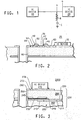
- FIG. 1 is a schematic illustration of a conventional (prior art) non-continuous load termination having a resistor and capacitor in series.
- FIG. 2 is a cross section view of a printed wiring board having a conventional (prior art) SMT RC transmission line termination for an integrated circuit device.
- FIGS. 4A-4F illustrate a method of making a laminate structure including the capacitive/resistive device illustrated in FIG. 3.
- Embodiments of the present invention are addressed to capacitive/resistive devices that may be buried in the substrate of a printed wiring board (PWB). Providing the capacitive and resistive functions within the PWB substrate conserves valuable surface real estate on the printed wiring board. The embodiments of the present invention also require fewer solder joints than conventional SMT termination arrangements.
- FIG. 3 is a section view of a portion of a printed wiring board 2000.
- the printed wiring board section 2000 includes an RC transmission line termination in which the resistor function and the capacitor function are integrated into a single capacitive/resistive device 200.
- the device 200 comprises a bottom electrode 210, a dielectric 220, a resistor element 230, a top electrode or top plate 240, and a conductive trace 245.
- the device 200 provides a resistive and a capacitive function in a single laminate structure, generally indicated by the bracket 201.
- the device 200 is coupled to an IC device 270 by the conductive circuit trace 245, a plated through hole via 250 extending through a dielectric layer 280, and a conductive circuit trace 260.
- the IC device 270 may be connected to the conductive circuit trace 260 by a solder pad 272 and a solder joint 274.
- a conductive circuit trace 211 may extend from the bottom electrode 210 for connection to other circuitry.
- FIGS. 4A-4F illustrate a method of making a laminate including the device 200.
- FIG. 4A is a section view in front elevation of a first stage of manufacture in which first and second metallic foils 212, 242 are provided.
- the second metallic foil 242 is provided with a layer of resistor material 232.
- the resistor material 232 can be, for example, NiP, CrSi, NiCr or other electrically resistive materials that can be plated or sputtered over the surface of the second metallic foil 242.
- the first and second metallic foils 212, 242 can be made from, for example, copper, copper-based materials, and other metals.
- a polymer solution may be cast or coated onto the first foil 212 and cured, forming a first dielectric layer 222.
- a similar, second dielectric layer 226 may be formed in a similar manner on the second foil 242, over the surface of the layer of resistor material 232.
- the polymer solution may be formed from, for example, epoxy, polyimide or other resins in a suitable solvent.
- a thin adhesive layer 227 may be applied to one or both surfaces of either of the dielectric layers 222, 226 (shown in FIG. 4A on the layer 222).
- the adhesive layer 227 may be formed from, for example, a thermoplastic polymer. The two structures are then laminated together in the direction of the arrows shown in FIG. 4A.
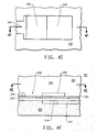
- FIG. 4C is a bottom section view of the resulting article, taken on line 4C-4C in FIG. 4D. Referring to FIG. 4C, the etching produces the bottom electrode 210 of the device 200 and the conductive circuit trace 211.
- FIG. 4D is a section view in front elevation taken on line 4D-4D in FIG. 4C.
- the bottom electrode 210 side of the resulting article is laminated to a laminate material 282.
- the lamination can be performed, for example, using FR4 prepreg, or other prepregs, in standard printing wiring board processes.
- FIG. 4E is a top section view of the resulting article, taken on line 4E-4E in FIG. 4F.
- FIG. 4F is a section view in front elevation, taken on line 4F-4F in FIG. 4E. Referring to FIGS. 4E and 4F, the etching produces the top electrode 240 of the device 200 and the conductive circuit trace 245. Etching images the foil 242 and the resistor layer 232.
- a dielectric layer 280 is laminated to the component side of the dielectric layer 282, forming a laminate structure 201.
- the laminate structure 201 can then be incorporated into, for example, a printed wiring board using conventional lamination and via formation processes.
- the electrodes 210, 240 are formed from copper foils.
- Resistive material 230 is a plated nickel phosphorus alloy of sheet resistivity 50 ohms per square.
- the dielectric 220 is an unfilled polyimide dielectric (INTERRA TM HK 04, available from DuPont Electronic Technologies, Wilmington, DE) of 25 microns thickness having a dielectric constant of 3.5 thereby giving a capacitance density of 800 picoFarads per square inch.
- the size (when viewed from a top plan perspective) of the capacitor needed for a transmission line termination of 30 picoFarad is 24.2 square mm, which corresponds to slightly less than 5 mm by 5 mm
- the size of the resistor in this example for a nominal 60 ohm resistance can be varied, as long as the length to width ratio is maintained at 1.2 to 1.0.
- the above capacitor is easy to make to relatively high tolerances.
- one piece of laminate can be used to embed many discrete resistors and many discrete capacitors, which reduces the inductance associated with connecting resistors and capacitors.
- the shapes of the capacitor embodiments in top plan view are generally rectangular.
- the capacitor electrodes, dielectrics, and other components and layers can have other regular or irregular surface area shapes, such as, for example, round, oblong, oval or polygonal shapes.
- a single capacitive/resistive device 200 is formed in the laminate structures 201 described above.
- panel structures and printed wiring boards can include a large number of individual capacitive/resistive devices of differing type and arrangement.
- resistance, capacitance and inductance combine to create a specific circuit impedance, typically identified by the capital letter Z.
- the resistance and capacitance may be structured to achieve a specific impedance. Changing the resistance, capacitance, or both will change the inductance. All three changes can be controlled to define the final impedance. In other words, the impedance of the laminate is tunable.
Landscapes
- Engineering & Computer Science (AREA)
- Microelectronics & Electronic Packaging (AREA)
- Production Of Multi-Layered Print Wiring Board (AREA)
- Parts Printed On Printed Circuit Boards (AREA)
- Fixed Capacitors And Capacitor Manufacturing Machines (AREA)
Applications Claiming Priority (1)
| Application Number | Priority Date | Filing Date | Title |
|---|---|---|---|
| US10/967,541 US7430128B2 (en) | 2004-10-18 | 2004-10-18 | Capacitive/resistive devices, organic dielectric laminates and printed wiring boards incorporating such devices, and methods of making thereof |
Publications (3)
| Publication Number | Publication Date |
|---|---|
| EP1651017A2 EP1651017A2 (en) | 2006-04-26 |
| EP1651017A3 EP1651017A3 (en) | 2006-05-03 |
| EP1651017B1 true EP1651017B1 (en) | 2007-08-01 |
Family
ID=35677559
Family Applications (1)
| Application Number | Title | Priority Date | Filing Date |
|---|---|---|---|
| EP05020898A Ceased EP1651017B1 (en) | 2004-10-18 | 2005-09-26 | RC devices, organic dielectric laminates and printed wiring boards incorporating such devices, and methods of making thereof |
Country Status (7)
| Country | Link |
|---|---|
| US (2) | US7430128B2 (https=) |
| EP (1) | EP1651017B1 (https=) |
| JP (1) | JP2006121086A (https=) |
| KR (1) | KR100677787B1 (https=) |
| CN (1) | CN1783379A (https=) |
| DE (1) | DE602005001826T2 (https=) |
| TW (1) | TWI402008B (https=) |
Families Citing this family (11)
| Publication number | Priority date | Publication date | Assignee | Title |
|---|---|---|---|---|
| US7345889B1 (en) * | 2004-09-28 | 2008-03-18 | Avaya Technology Corp. | Method and system for reducing radiated energy emissions in computational devices |
| US7596842B2 (en) * | 2005-02-22 | 2009-10-06 | Oak-Mitsui Inc. | Method of making multilayered construction for use in resistors and capacitors |
| JP2015233084A (ja) * | 2014-06-10 | 2015-12-24 | 株式会社日立製作所 | チップモジュールおよび情報処理機器 |
| CN105047411A (zh) * | 2015-08-12 | 2015-11-11 | 深圳市槟城电子有限公司 | 一种电阻和电容串连的组件及其制作方法 |
| CN105047642B (zh) * | 2015-08-12 | 2024-01-19 | 深圳市槟城电子股份有限公司 | 一种端口防护电路集成封装件 |
| WO2017154167A1 (ja) * | 2016-03-10 | 2017-09-14 | 三井金属鉱業株式会社 | 多層積層板及びこれを用いた多層プリント配線板の製造方法 |
| TWI694752B (zh) * | 2018-10-26 | 2020-05-21 | 鼎展電子股份有限公司 | 內嵌式被動元件結構 |
| EP3761492B1 (en) * | 2019-07-05 | 2023-01-04 | Infineon Technologies AG | Snubber circuit and power semiconductor module with snubber circuit |
| CN114695131A (zh) * | 2022-03-24 | 2022-07-01 | 广东佛智芯微电子技术研究有限公司 | 一种扇出型封装基板结构及其制备方法 |
| WO2024086219A1 (en) * | 2022-10-21 | 2024-04-25 | KYOCERA AVX Components Corporation | Single layer capacitor |
| DE112024002007T5 (de) * | 2023-05-10 | 2026-02-26 | KYOCERA AVX Components Corporation | Abscheidbarer einzelschichtkondensator |
Family Cites Families (44)
| Publication number | Priority date | Publication date | Assignee | Title |
|---|---|---|---|---|
| US3934119A (en) | 1974-09-17 | 1976-01-20 | Texas Instruments Incorporated | Electrical resistance heaters |
| US4377652A (en) | 1978-02-17 | 1983-03-22 | Asahi Kasei Kogyo Kabushiki Kaisha | Polyamide-imide compositions and articles for electrical use prepared therefrom |
| US4410867A (en) * | 1978-12-28 | 1983-10-18 | Western Electric Company, Inc. | Alpha tantalum thin film circuit device |
| DE2903025C2 (de) | 1979-01-26 | 1983-05-05 | Siemens AG, 1000 Berlin und 8000 München | RC-Netzwerk |
| US4407883A (en) | 1982-03-03 | 1983-10-04 | Uop Inc. | Laminates for printed circuit boards |
| JPS58190091A (ja) | 1982-04-30 | 1983-11-05 | 宇部興産株式会社 | フレキシブル配線基板の製造方法 |
| JPS59144162A (ja) | 1983-02-08 | 1984-08-18 | Nec Corp | 薄膜回路の製造方法 |
| JPS60113993A (ja) | 1983-11-25 | 1985-06-20 | 三菱電機株式会社 | 多層回路基板の製造方法 |
| US5354695A (en) * | 1992-04-08 | 1994-10-11 | Leedy Glenn J | Membrane dielectric isolation IC fabrication |
| US5093036A (en) | 1988-09-20 | 1992-03-03 | Raychem Corporation | Conductive polymer composition |
| JP2764745B2 (ja) | 1989-07-21 | 1998-06-11 | オムロン株式会社 | 混成回路基板およびその製造方法 |
| JP2802173B2 (ja) * | 1990-02-06 | 1998-09-24 | 松下電工株式会社 | 複合誘電体 |
| JPH04211191A (ja) * | 1990-02-09 | 1992-08-03 | Hitachi Ltd | 実装構造体 |
| JP3019541B2 (ja) | 1990-11-22 | 2000-03-13 | 株式会社村田製作所 | コンデンサ内蔵型配線基板およびその製造方法 |
| JPH0565456A (ja) | 1991-09-09 | 1993-03-19 | Sumitomo Bakelite Co Ltd | 気密封止用樹脂ペースト |
| DE69305942T2 (de) | 1992-09-15 | 1997-03-13 | Du Pont | Zusammensetzung für einen Polymer-Dickschichtwiderstand |
| US6111005A (en) | 1993-07-30 | 2000-08-29 | Diemat, Inc. | Polymeric adhesive paste |
| US6140402A (en) | 1993-07-30 | 2000-10-31 | Diemat, Inc. | Polymeric adhesive paste |
| JPH07161578A (ja) * | 1993-12-06 | 1995-06-23 | Rubikon Denshi Kk | フィルムコンデンサの製造方法 |
| JPH07226334A (ja) * | 1994-02-09 | 1995-08-22 | Matsushita Electric Ind Co Ltd | 薄膜コンデンサ及びその製造方法 |
| JP3117175B2 (ja) | 1994-02-09 | 2000-12-11 | アルプス電気株式会社 | 抵抗体 |
| TW301843B (en) | 1994-11-15 | 1997-04-01 | Ibm | Electrically conductive paste and composite and their use as an electrically conductive connector |
| JP3684239B2 (ja) * | 1995-01-10 | 2005-08-17 | 株式会社 日立製作所 | 低emi電子機器 |
| TW367621B (en) | 1995-02-27 | 1999-08-21 | Nxp Bv | Electronic component comprising a thin-film structure with passive elements |
| US5874770A (en) | 1996-10-10 | 1999-02-23 | General Electric Company | Flexible interconnect film including resistor and capacitor layers |
| US5993698A (en) | 1997-11-06 | 1999-11-30 | Acheson Industries, Inc. | Electrical device containing positive temperature coefficient resistor composition and method of manufacturing the device |
| JP2000269079A (ja) * | 1999-03-19 | 2000-09-29 | Dainippon Printing Co Ltd | 共振回路及びその製造方法 |
| US6114015A (en) * | 1998-10-13 | 2000-09-05 | Matsushita Electronic Materials, Inc. | Thin-laminate panels for capacitive printed-circuit boards and methods for making the same |
| US6030553A (en) | 1999-04-01 | 2000-02-29 | Industrial Technology Research Institute | Polymer thick film resistor pastes |
| US6285542B1 (en) | 1999-04-16 | 2001-09-04 | Avx Corporation | Ultra-small resistor-capacitor thin film network for inverted mounting to a surface |
| US6356455B1 (en) * | 1999-09-23 | 2002-03-12 | Morton International, Inc. | Thin integral resistor/capacitor/inductor package, method of manufacture |
| JP2001310911A (ja) * | 2000-04-28 | 2001-11-06 | Sumitomo Seika Chem Co Ltd | 誘電体形成物質及び誘電体フィルム |
| US6278356B1 (en) | 2000-05-17 | 2001-08-21 | Compeq Manufacturing Company Limited | Flat, built-in resistors and capacitors for a printed circuit board |
| JP4224190B2 (ja) * | 2000-06-20 | 2009-02-12 | パナソニック電工株式会社 | プリント配線板の製造方法及びプリント配線板 |
| US6541137B1 (en) * | 2000-07-31 | 2003-04-01 | Motorola, Inc. | Multi-layer conductor-dielectric oxide structure |
| JP2002252297A (ja) * | 2001-02-23 | 2002-09-06 | Hitachi Ltd | 多層回路基板を用いた電子回路装置 |
| EP1265466A3 (en) * | 2001-06-05 | 2004-07-21 | Dai Nippon Printing Co., Ltd. | Method for fabrication wiring board provided with passive element and wiring board provided with passive element |
| JP2003142590A (ja) * | 2001-11-06 | 2003-05-16 | Matsushita Electric Ind Co Ltd | 容量素子 |
| JP3711343B2 (ja) * | 2002-06-26 | 2005-11-02 | 株式会社トッパンNecサーキットソリューションズ | 印刷配線板及びその製造方法並びに半導体装置 |
| US6600645B1 (en) | 2002-09-27 | 2003-07-29 | Ut-Battelle, Llc | Dielectric composite materials and method for preparing |
| JP2004214586A (ja) * | 2002-11-14 | 2004-07-29 | Kyocera Corp | 多層配線基板 |
| JP2004193411A (ja) * | 2002-12-12 | 2004-07-08 | Fujikura Ltd | 高誘電率電気・電子部品の製造方法と部品 |
| US6910264B2 (en) | 2003-01-03 | 2005-06-28 | Phoenix Precision Technology Corp. | Method for making a multilayer circuit board having embedded passive components |
| JP2004214573A (ja) | 2003-01-09 | 2004-07-29 | Murata Mfg Co Ltd | セラミック多層基板の製造方法 |
-
2004
- 2004-10-18 US US10/967,541 patent/US7430128B2/en not_active Expired - Lifetime
-
2005
- 2005-09-26 EP EP05020898A patent/EP1651017B1/en not_active Ceased
- 2005-09-26 DE DE602005001826T patent/DE602005001826T2/de active Active
- 2005-10-04 TW TW094134606A patent/TWI402008B/zh not_active IP Right Cessation
- 2005-10-17 KR KR1020050097350A patent/KR100677787B1/ko not_active Expired - Fee Related
- 2005-10-18 CN CNA2005101161088A patent/CN1783379A/zh active Pending
- 2005-10-18 JP JP2005303550A patent/JP2006121086A/ja active Pending
-
2008
- 2008-08-08 US US12/188,271 patent/US7813141B2/en not_active Expired - Fee Related
Non-Patent Citations (1)
| Title |
|---|
| None * |
Also Published As
| Publication number | Publication date |
|---|---|
| US20080297274A1 (en) | 2008-12-04 |
| US7430128B2 (en) | 2008-09-30 |
| DE602005001826T2 (de) | 2008-04-24 |
| JP2006121086A (ja) | 2006-05-11 |
| KR100677787B1 (ko) | 2007-02-02 |
| TW200635454A (en) | 2006-10-01 |
| US20060082980A1 (en) | 2006-04-20 |
| DE602005001826D1 (de) | 2007-09-13 |
| KR20060054031A (ko) | 2006-05-22 |
| CN1783379A (zh) | 2006-06-07 |
| EP1651017A3 (en) | 2006-05-03 |
| TWI402008B (zh) | 2013-07-11 |
| US7813141B2 (en) | 2010-10-12 |
| EP1651017A2 (en) | 2006-04-26 |
Similar Documents
| Publication | Publication Date | Title |
|---|---|---|
| EP1648208B1 (en) | Capacitive/resistive devices and printed wiring boards incorporating such devices, and methods of making thereof | |
| US7813141B2 (en) | Capacitive/resistive devices, organic dielectric laminates and printed wiring boards incorporating such devices, and methods of making thereof | |
| US6021050A (en) | Printed circuit boards with integrated passive components and method for making same | |
| US20050156906A1 (en) | Capacitive touchpad and method for forming the same | |
| US20060286696A1 (en) | Passive electrical article | |
| EP1648207B1 (en) | Capacitive/Resistive devices, high dielectric constant organic dielectric laminates and printed wiring boards incorporating such devices, and methods of making thereof | |
| EP1720393A3 (en) | Multilayered printed wiring board and its manufacture | |
| US20190281707A1 (en) | Method for manufacturing an embedded flexible circuit board | |
| US20020020553A1 (en) | Method and component for forming an embedded resistor in a multi-layer printed circuit | |
| US6713399B1 (en) | Carbon-conductive ink resistor printed circuit board and its fabrication method | |
| JP4207517B2 (ja) | 素子内蔵基板 | |
| JP4684483B2 (ja) | 多層回路基板の製造方法 | |
| JP3474895B2 (ja) | 電気接続装置とその製造方法ならびにプリント配線板とその製造方法 |
Legal Events
| Date | Code | Title | Description |
|---|---|---|---|
| PUAI | Public reference made under article 153(3) epc to a published international application that has entered the european phase |
Free format text: ORIGINAL CODE: 0009012 |
|
| PUAL | Search report despatched |
Free format text: ORIGINAL CODE: 0009013 |
|
| AK | Designated contracting states |
Kind code of ref document: A2 Designated state(s): AT BE BG CH CY CZ DE DK EE ES FI FR GB GR HU IE IS IT LI LT LU LV MC NL PL PT RO SE SI SK TR |
|
| AX | Request for extension of the european patent |
Extension state: AL BA HR MK YU |
|
| AK | Designated contracting states |
Kind code of ref document: A3 Designated state(s): AT BE BG CH CY CZ DE DK EE ES FI FR GB GR HU IE IS IT LI LT LU LV MC NL PL PT RO SE SI SK TR |
|
| AX | Request for extension of the european patent |
Extension state: AL BA HR MK YU |
|
| 17P | Request for examination filed |
Effective date: 20060529 |
|
| 17Q | First examination report despatched |
Effective date: 20060711 |
|
| AKX | Designation fees paid |
Designated state(s): DE FR GB |
|
| GRAP | Despatch of communication of intention to grant a patent |
Free format text: ORIGINAL CODE: EPIDOSNIGR1 |
|
| GRAS | Grant fee paid |
Free format text: ORIGINAL CODE: EPIDOSNIGR3 |
|
| GRAA | (expected) grant |
Free format text: ORIGINAL CODE: 0009210 |
|
| AK | Designated contracting states |
Kind code of ref document: B1 Designated state(s): DE FR GB |
|
| REG | Reference to a national code |
Ref country code: GB Ref legal event code: FG4D |
|
| REF | Corresponds to: |
Ref document number: 602005001826 Country of ref document: DE Date of ref document: 20070913 Kind code of ref document: P |
|
| ET | Fr: translation filed | ||
| PLBE | No opposition filed within time limit |
Free format text: ORIGINAL CODE: 0009261 |
|
| STAA | Information on the status of an ep patent application or granted ep patent |
Free format text: STATUS: NO OPPOSITION FILED WITHIN TIME LIMIT |
|
| 26N | No opposition filed |
Effective date: 20080506 |
|
| REG | Reference to a national code |
Ref country code: FR Ref legal event code: TP Owner name: CDA PROCESSING COMPANY LIMITED LIABILITY COMPA, US Effective date: 20120321 |
|
| REG | Reference to a national code |
Ref country code: GB Ref legal event code: 732E Free format text: REGISTERED BETWEEN 20120329 AND 20120404 |
|
| REG | Reference to a national code |
Ref country code: DE Ref legal event code: R081 Ref document number: 602005001826 Country of ref document: DE Owner name: CDA PROCESSING LIMITED LIABILITY COMPANY, WILM, US Free format text: FORMER OWNER: E.I. DU PONT DE NEMOURS AND CO., WILMINGTON, DEL., US Effective date: 20120625 |
|
| REG | Reference to a national code |
Ref country code: FR Ref legal event code: PLFP Year of fee payment: 12 |
|
| REG | Reference to a national code |
Ref country code: FR Ref legal event code: PLFP Year of fee payment: 13 |
|
| REG | Reference to a national code |
Ref country code: FR Ref legal event code: PLFP Year of fee payment: 14 |
|
| PGFP | Annual fee paid to national office [announced via postgrant information from national office to epo] |
Ref country code: GB Payment date: 20220810 Year of fee payment: 18 Ref country code: DE Payment date: 20220615 Year of fee payment: 18 |
|
| PGFP | Annual fee paid to national office [announced via postgrant information from national office to epo] |
Ref country code: FR Payment date: 20220810 Year of fee payment: 18 |
|
| P01 | Opt-out of the competence of the unified patent court (upc) registered |
Effective date: 20230527 |
|
| REG | Reference to a national code |
Ref country code: DE Ref legal event code: R119 Ref document number: 602005001826 Country of ref document: DE |
|
| GBPC | Gb: european patent ceased through non-payment of renewal fee |
Effective date: 20230926 |
|
| PG25 | Lapsed in a contracting state [announced via postgrant information from national office to epo] |
Ref country code: GB Free format text: LAPSE BECAUSE OF NON-PAYMENT OF DUE FEES Effective date: 20230926 |
|
| PG25 | Lapsed in a contracting state [announced via postgrant information from national office to epo] |
Ref country code: GB Free format text: LAPSE BECAUSE OF NON-PAYMENT OF DUE FEES Effective date: 20230926 Ref country code: FR Free format text: LAPSE BECAUSE OF NON-PAYMENT OF DUE FEES Effective date: 20230930 Ref country code: DE Free format text: LAPSE BECAUSE OF NON-PAYMENT OF DUE FEES Effective date: 20240403 |