EP1589594A1 - Gross-manetowiderstandseffektelement des ccp-typs und magnetische komponente und magnetische einrichtung damit - Google Patents
Gross-manetowiderstandseffektelement des ccp-typs und magnetische komponente und magnetische einrichtung damit Download PDFInfo
- Publication number
- EP1589594A1 EP1589594A1 EP04704713A EP04704713A EP1589594A1 EP 1589594 A1 EP1589594 A1 EP 1589594A1 EP 04704713 A EP04704713 A EP 04704713A EP 04704713 A EP04704713 A EP 04704713A EP 1589594 A1 EP1589594 A1 EP 1589594A1
- Authority
- EP
- European Patent Office
- Prior art keywords
- layer
- magnetic
- giant magnetoresistance
- cpp
- type giant
- Prior art date
- Legal status (The legal status is an assumption and is not a legal conclusion. Google has not performed a legal analysis and makes no representation as to the accuracy of the status listed.)
- Granted
Links
Images




Classifications
-
- B—PERFORMING OPERATIONS; TRANSPORTING
- B82—NANOTECHNOLOGY
- B82Y—SPECIFIC USES OR APPLICATIONS OF NANOSTRUCTURES; MEASUREMENT OR ANALYSIS OF NANOSTRUCTURES; MANUFACTURE OR TREATMENT OF NANOSTRUCTURES
- B82Y10/00—Nanotechnology for information processing, storage or transmission, e.g. quantum computing or single electron logic
-
- B—PERFORMING OPERATIONS; TRANSPORTING
- B82—NANOTECHNOLOGY
- B82Y—SPECIFIC USES OR APPLICATIONS OF NANOSTRUCTURES; MEASUREMENT OR ANALYSIS OF NANOSTRUCTURES; MANUFACTURE OR TREATMENT OF NANOSTRUCTURES
- B82Y25/00—Nanomagnetism, e.g. magnetoimpedance, anisotropic magnetoresistance, giant magnetoresistance or tunneling magnetoresistance
-
- G—PHYSICS
- G01—MEASURING; TESTING
- G01R—MEASURING ELECTRIC VARIABLES; MEASURING MAGNETIC VARIABLES
- G01R33/00—Arrangements or instruments for measuring magnetic variables
- G01R33/02—Measuring direction or magnitude of magnetic fields or magnetic flux
- G01R33/06—Measuring direction or magnitude of magnetic fields or magnetic flux using galvano-magnetic devices
- G01R33/09—Magnetoresistive devices
- G01R33/093—Magnetoresistive devices using multilayer structures, e.g. giant magnetoresistance sensors
-
- G—PHYSICS
- G11—INFORMATION STORAGE
- G11C—STATIC STORES
- G11C11/00—Digital stores characterised by the use of particular electric or magnetic storage elements; Storage elements therefor
- G11C11/02—Digital stores characterised by the use of particular electric or magnetic storage elements; Storage elements therefor using magnetic elements
- G11C11/14—Digital stores characterised by the use of particular electric or magnetic storage elements; Storage elements therefor using magnetic elements using thin-film elements
- G11C11/15—Digital stores characterised by the use of particular electric or magnetic storage elements; Storage elements therefor using magnetic elements using thin-film elements using multiple magnetic layers
-
- H—ELECTRICITY
- H01—ELECTRIC ELEMENTS
- H01F—MAGNETS; INDUCTANCES; TRANSFORMERS; SELECTION OF MATERIALS FOR THEIR MAGNETIC PROPERTIES
- H01F10/00—Thin magnetic films, e.g. of one-domain structure
- H01F10/32—Spin-exchange-coupled multilayers, e.g. nanostructured superlattices
- H01F10/324—Exchange coupling of magnetic film pairs via a very thin non-magnetic spacer, e.g. by exchange with conduction electrons of the spacer
- H01F10/3268—Exchange coupling of magnetic film pairs via a very thin non-magnetic spacer, e.g. by exchange with conduction electrons of the spacer the exchange coupling being asymmetric, e.g. by use of additional pinning, by using antiferromagnetic or ferromagnetic coupling interface, i.e. so-called spin-valve [SV] structure, e.g. NiFe/Cu/NiFe/FeMn
- H01F10/3272—Exchange coupling of magnetic film pairs via a very thin non-magnetic spacer, e.g. by exchange with conduction electrons of the spacer the exchange coupling being asymmetric, e.g. by use of additional pinning, by using antiferromagnetic or ferromagnetic coupling interface, i.e. so-called spin-valve [SV] structure, e.g. NiFe/Cu/NiFe/FeMn by use of anti-parallel coupled [APC] ferromagnetic layers, e.g. artificial ferrimagnets [AFI], artificial [AAF] or synthetic [SAF] anti-ferromagnets
- H01F10/3277—Exchange coupling of magnetic film pairs via a very thin non-magnetic spacer, e.g. by exchange with conduction electrons of the spacer the exchange coupling being asymmetric, e.g. by use of additional pinning, by using antiferromagnetic or ferromagnetic coupling interface, i.e. so-called spin-valve [SV] structure, e.g. NiFe/Cu/NiFe/FeMn by use of anti-parallel coupled [APC] ferromagnetic layers, e.g. artificial ferrimagnets [AFI], artificial [AAF] or synthetic [SAF] anti-ferromagnets by use of artificial ferrimagnets [AFI] only
-
- H—ELECTRICITY
- H10—SEMICONDUCTOR DEVICES; ELECTRIC SOLID-STATE DEVICES NOT OTHERWISE PROVIDED FOR
- H10B—ELECTRONIC MEMORY DEVICES
- H10B61/00—Magnetic memory devices, e.g. magnetoresistive RAM [MRAM] devices
-
- H—ELECTRICITY
- H10—SEMICONDUCTOR DEVICES; ELECTRIC SOLID-STATE DEVICES NOT OTHERWISE PROVIDED FOR
- H10N—ELECTRIC SOLID-STATE DEVICES NOT OTHERWISE PROVIDED FOR
- H10N50/00—Galvanomagnetic devices
- H10N50/10—Magnetoresistive devices
-
- G—PHYSICS
- G11—INFORMATION STORAGE
- G11B—INFORMATION STORAGE BASED ON RELATIVE MOVEMENT BETWEEN RECORD CARRIER AND TRANSDUCER
- G11B5/00—Recording by magnetisation or demagnetisation of a record carrier; Reproducing by magnetic means; Record carriers therefor
- G11B5/127—Structure or manufacture of heads, e.g. inductive
- G11B5/33—Structure or manufacture of flux-sensitive heads, i.e. for reproduction only; Combination of such heads with means for recording or erasing only
- G11B5/39—Structure or manufacture of flux-sensitive heads, i.e. for reproduction only; Combination of such heads with means for recording or erasing only using magneto-resistive devices or effects
- G11B2005/3996—Structure or manufacture of flux-sensitive heads, i.e. for reproduction only; Combination of such heads with means for recording or erasing only using magneto-resistive devices or effects large or giant magnetoresistive effects [GMR], e.g. as generated in spin-valve [SV] devices
Definitions
- the present invention relates to a giant magnetoresistance device that exhibits a giant magnetoresistance effect by spin dependent current in a direction perpendicular to a film plane (hereinafter referred to as "CPP type giant magnetoresistance device”) and also to magnetic components and units using the same.
- CPP type giant magnetoresistance device a giant magnetoresistance device that exhibits a giant magnetoresistance effect by spin dependent current in a direction perpendicular to a film plane
- GMR giant magnetoresistance
- GMR devices have already been put to practical use as in magnetic sensors and reproducing heads in hard disk drives. Then, current is passed in a film plane, when the GMR device is called “CIP-GMR” device where CIP stands for Current In Plane.
- the CIP-GMR device generally makes use of an element called what is of spin valve in which an antiferromagnet is brought adjacent to one of the ferromagnets to fix spins in the one ferromagnet.
- CCPP Current Perpendicular to the Plane
- CPP-GMR is greater in magnitude than CIP-GMR.
- CPP-GMR there is the proposed development to a CPP-type giant magnetoresistive effect device in which spiral magnetic domains generated by a sense current in a free magnetic layer are controlled to develop and then to a reproducing head using the device. See, the Japanese laid open patent application, for example, JP 2002-359415 A.
- a CPP-GMR device so far proposed is small in resistance, however, since its current path is small. Being poor in utility unless it is made enough smaller, the device has not yet been put to practical use.
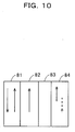
- the spin valve type has been considered having an antiferromagnetic layer 81 brought adjacent to a ferromagnetic fixed layer 82 as shown in Fig. 10, the antiferromagnetic layer 81 is larger in resistance than a GMR film made of a ferromagnetic free layer 84, a nonmagnetic conductive layer 83 and the ferromagnetic fixed layer 82 to an extent that the spin valve element then will generally have to have its rate of resistance change as small as less than 1 % and its resistance change ⁇ R that is small, too. This becomes a primary and large factor that prevents a CPP-GMR device from its practical use.
- the present inventors have discovered that coupling a pair of ferromagnetic layers antiparallel to each other via a nonmagnetic metal layer while using this three-layer structure (SyAF) with different magnitudes of magnetization for a free and/or a fixed layer gives rise to a CPP-GMR device of spin valve type of which ⁇ R is large and the rate of change of magnetic resistance is increased to 8 % or more and then have reached the present invention.
- SyAF three-layer structure
- a CPP type giant magnetoresistance device having a ferromagnetic fixed layer, a nonmagnetic conductive layer and a ferromagnetic free layer, characterized in that the said ferromagnetic free layer has a first and a second magnetic layer magnetically coupled together antiparallel to each other via a magnetic coupler and formed to have different magnitudes of magnetization from each other wherein the said first and second magnetic layers are adapted to reverse their magnetizations jointly while maintaining their mutual antiparallel state of magnetization.
- the device of the present invention as set forth in claim 2 is further characterized in that the said magnetic coupler in the said ferromagnetic free layer forms an interface that is responsive to a spin dependent current of said ferromagnetic fixed layer for scattering spin dependent electrons.
- the device of the present invention as set forth in claim 3 is further characterized in that a plurality of such ferromagnetic free layers are laid one upon another to increase its CPP-GMR.
- the device of the present invention as set forth in claim 4 is further characterized in that the first and second magnetic layers in the said ferromagnetic free layer have an aspect ratio not greater than 2.
- the device of the present invention as set forth in claim 5 is further characterized in that, in addition to the makeup mentioned above, the said magnetic coupler comprises a nonmagnetic metal or semiconductor layer.
- the device of the present invention as set forth in claim 6 is further characterized in that the said magnetic coupler comprises an alloy containing any one or more or of any combination, or a multi-layer of any combination, of ruthenium, iridium, rhodium, rhenium and chromium.
- the device of the present invention as set forth in claim 7 is further characterized in that the said magnetic coupler is in the form of a thin film having a film thickness of not greater than 1.5 nm.
- the device of the present invention as set forth in claim 8 is further characterized in that the said nonmagnetic conductive layer is made of cupper as a material bringing about large spin dependent scattering.
- the device of the present invention as set forth in claim 9 is further characterized in that the said ferromagnetic fixed layer is of spin valve type having a ferromagnetic layer and an antiferromagnetic layer placed adjacent thereto.
- a CPP type giant magnetoresistance device constructed as mentioned above exhibits a CPP-GMR increased by spin dependent scattering brought about at an interface with the magnetic coupler in the ferromagnetic free layer in accordance with directions of magnetizations of the ferromagnetic fixed and free layers.
- the CPP type giant magnetoresistance device in this aspect of the present invention can thus have its CPP-GMR extremely increased.
- a CPP type giant magnetoresistance device having a ferromagnetic fixed layer, a nonmagnetic conductive layer and a ferromagnetic free layer, characterized in that the said ferromagnetic fixed layer has a first and a second magnetic layer magnetically coupled together antiparallel to each other via a magnetic coupler and formed to have different magnitudes of magnetization from each other.
- the device in this aspect of the present invention as set forth in claim 11 is further characterized in that the said ferromagnetic free layer has a first and a second magnetic layer magnetically coupled together antiparallel to each other via a magnetic coupler and formed to have different magnitudes of magnetization from each other wherein the said first and second magnetic layers are adapted to reverse their magnetizations jointly while maintaining their mutual antiparallel state of magnetization.
- the device in this aspect of the present invention as set forth in claim 12 is further characterized in that the said magnetic coupler comprises a nonmagnetic metal layer made of one or more of ruthenium, iridium, rhodium, rhenium and chromium.
- a CPP type giant magnetoresistance device constructed as mentioned above exhibits a CPP-GMR increased by spin dependent scattering brought about at an interface with the magnetic coupler in the ferromagnetic free layer and/or at an interface in the ferromagnetic fixed layer in accordance with directions of magnetizations of the ferromagnetic fixed and free layers.
- the CPP type giant magnetoresistance device in this aspect of the present invention can thus have its CPP-GMR extremely increased.
- a CPP type giant magnetoresistance device having a ferromagnetic fixed layer, a nonmagnetic conductive layer and a ferromagnetic free layer, characterized in that it has a layer made of one or more of ruthenium, iridium, rhodium, rhenium and chromium between the said ferromagnetic fixed and nonmagnetic conductive layers and/or on a surface of the said ferromagnetic free layer.
- a CPP type giant magnetoresistance device constructed as mentioned above exhibits a CPP-GMR increased by spin dependent scattering brought about at interfaces of the nonmagnetic metal layer with the ferromagnetic fixed layer and with the nonmagnetic conductive layer and/or at an interface between the nonmagnetic metal layer and the ferromagnetic free layer in accordance with directions of magnetizations of the ferromagnetic fixed and free layers.
- the CPP type giant magnetoresistance device in this aspect of the present invention can thus have its CPP-GMR extremely increased.
- a magnetic component using a CPP type giant magnetoresistance device characterized by having a CPP type giant magnetoresistance device as set forth in any one of claims 1 to 13.
- the present invention also provides as set forth in claim 15, a magnetic head for reading recorded information by detecting a leakage magnetic field from a recording medium, characterized in that it comprises a CPP type giant magnetoresistance device as set forth in any one of claims 1 to 13, wherein a said ferromagnetic free layer is adapted to reverse its magnetization in response to a leakage magnetic field from the said recording medium to cause the device to exhibit CPP-GMR based on spin dependent scattering of sensor electrons, thereby detecting a direction of the said leakage magnetic field as a change in resistance.
- the magnetic head of the present invention as set forth in claim 16 is further characterized in that, in addition to the makeup mentioned above, the second magnetic layer in said ferromagnetic free layer has an end face set face to face with the said recording medium for detecting the leakage magnetic field therefrom.
- the magnetic head of the present invention as set forth in claim 17 is further characterized in that a stratal end face of the said ferromagnetic free layer on which its multi-layered structure appears is set face to face with the said recording medium for detecting the leakage magnetic field therefrom.
- the magnetic head of the present invention as set forth in claim 18 is further characterized by comprising an electrode for supplying sensor electrons to the CPP type giant magnetoresistance device, the said electrode also serving as a magnetic shield against the leakage magnetic field from the said recording medium.
- a magnetic component can have an electrical resistance therein varied by the CPP-GMR that the device exhibits and which is increased by spin dependent scattering in the device.
- the magnetic component of the present invention can thus detect a direction of a magnetic field as a change in electrical resistance.
- a magnetic unit using a CPP type giant magnetoresistance device characterized by having a CPP type giant magnetoresistance device as set forth in any one of claims 1 to 13.
- the present invention also provides as set forth in claim 20, a magnetic recorder characterized in that a CPP type giant magnetoresistance device as set forth in any one of claims 1 to 13 is arranged to lie at each of intersections of word lines and bit lines to form a nonvolatile storage.
- the magnetic recorder of the present invention as set forth in claim 21 is further characterized in that the said ferromagnetic free layer is adapted to reverse its magnetic field in response to spin injection from each such word line.
- a magnetic recorder constructed as mentioned above allows writing or reading by passing a spin dependent current.
- the magnetic recorder of the present invention provides nonvolatile magnetic storage capability and its operation only requires a spin dependent current to be passed.
- Fig. 1 depicts in conceptual views a CPP type giant magnetoresistance device of spin valve type according to a first form of implementation of the present invention wherein a first magnetic layer in a ferromagnetic free layer and a fixed layer are magnetized antiparallel and parallel to each other as shown at (a) and (b), respectively.
- a first magnetic layer in a ferromagnetic free layer and a fixed layer are magnetized antiparallel and parallel to each other as shown at (a) and (b), respectively.
- the CPP type giant magnetoresistance device of the first form of implementation here designated by reference character 10
- These layers of the multi-layered structure are formed each having a film thickness of a nanometer size.
- This nanometer size means a size such that an electron while conserving its momentum and spin is capable of conducting.
- spins in a device of this size can, without relaxing, flow from one side into another.
- the CPP type giant magnetoresistance device of spin valve type includes the antiferromagnetic layer 9 adjacent to the ferromagnetic fixed layer 11 as a fixed layer
- the antiferromagnetic layer 9 may be omitted when the ferromagnetic fixed layer 11 is formed of a film having a coercive force large enough for it alone to serve as a fixed layer.
- the nonmagnetic conductive layer 12 should effectively be a metal layer made of copper (Cu). Cu allows giving rise to much larger spin dependent scattering than the other metals capable of spin dependent scattering.
- the ferromagnetic free layer 13 is shown here as having applied thereto or to a free layer, a three-layer structure in which two ferromagnetic layers, namely the first and second magnetic layers 14 and 16, are magnetically coupled together antiparallel to each other via the magnetic coupler 15 and formed to have different magnitudes of magnetization from each other.
- This three-layer structure according to the present invention will also be referred to hereinafter as "SyAF” that stands for "Synthetic Anti-Ferromagnet".
- the ferromagnetic free layer 13 may not only be made up of this three-layer structure singly, but also it may comprise a multi-layer of more than one such three-layer structural units to increase the device's CPP-GMR.
- the first and second magnetic layers 14 and 16 are composed of an identical material, then they may be formed to have a difference in film thickness and thereby to make a difference in magnitude of magnetization between them.
- Magnetizations 17 and 18 of the first and second magnetic layers 14 and 16 are here capable of being jointly reversed e. g., under flux reversing magnetic field applied externally, while maintaining their mutual antiparallel relationship of magnetization.
- the magnetic coupler 15 has a function of antiferromagnetic coupling.
- a nonmagnetic metal or semiconductor may be used to form the magnetic coupler 15.
- a FeSi alloy and Si as a semiconductor element may be utilized.
- the magnetic coupler 15 in the form of a layer should preferably have a film thickness as thin as 1.5 nm or less. Forming it in a thin film of 1.5 nm or less brings about strong antiparallel exchange coupling and is thus advantageous.
- CPP-GMR ⁇ (A + B) AF - (A + B) F ⁇ / ⁇ (A + B) F + C ⁇
- subscripts "F” and "AF” mean the magnetizations of the free layer and fixed layers being parallel and antiparallel to each other, respectively. From the above it can be seen that the larger the resistance C excessively than the resistance (A + B), the smaller the CPP-GMR.
- the SyAF being the three-layer structure will make its resistance larger than a monolayer film but not much as an antiferromagnet. For this reason, with this effect alone it is not expected that the use of a SyAF for a free layer would give rise to an extreme increase in CPP-GMR.
- the present inventors have found, however, that the CPP-GMR device made with the SyAF used for the ferromagnetic free layer 13 has a CPP-GMR that is increased by 8 % or more, or one figure larger, than that which has hitherto be obtained.
- an electron 6 as shown with its spin ( ⁇ ) oriented downwards the same as the magnetization 17 of the first magnetic layer 14 will not be scattered at the interface between the nonmagnetic conductive layer 12 and the first magnetic layer 14 and will be scattered intensely at the interface between the first magnetic layer 14 and the Ruthenium layer 15. Electrons so scattered will then be scattered at the interface between the nonmagnetic conductive layer 12 and the ferromagnetic fixed layer 11. As a result, electrons of these two classes different in pin orientation will have paths of conduction as indicated by refracted lines 1 and 2, respectively, in Fig. 1(a).
- the electrons 5 with upwards spins ( ⁇ ) which are scattered at the Ruthenium 15 interface will not be scattered at the interface between the ferromagnetic fixed layer 11 and the nonmagnetic conductive layer 12 and will be scattered at the interface between the antiferromagnetic layer 9 and the ferromagnetic fixed layer 11. In the meantime, the electrons 5 whose mean free path is thus long will each be able to make a number of round rips while having its spin conserved.
- the electrons 6 with downward spins ( ⁇ ) will, as in Fig. 1(a), be scattered at the interface between the nonmagnetic conductive layer 12 and the first magnetic layer 14.
- the conduction paths of these electrons are indicated by refracted lines 3 and 4 as shown in Fig. 1(b).
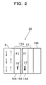
- Fig. 2 is a cross sectional view illustrating the makeup of a CPP type giant magnetoresistance device of spin valve type according to the second form of implementation of the present invention.
- a CPP type giant magnetoresistance device 20 according to the second form of implementation, which has a multi-layered structure comprising an antiferromagnetic layer 9, a ferromagnetic fixed layer 11A, a nonmagnetic conductive layer 12 and a ferromagnetic free layer 13A.
- the ferromagnetic fixed layer 11A has a SyAF structure wherein the ferromagnetic fixed layer 11A has a first magnetic layer 14A and a second magnetic layer 16A which are coupled together magnetically antiparallel to each other via a magnetic coupler 15A and formed to have different magnitudes of magnetization 17' and 18', respectively.
- These layers of the multi-layered structure are formed each having a film thickness of a nanometer size.
- the magnetic coupler 15A in the SyAF structure one or more of ruthenium, iridium, rhodium, rhenium and chromium may be used. More than one of them may be used in the form of a multi-layer or an alloy body to constitute the coupler. In addition, a FeSi alloy and Si as a semiconductor element may be utilized. Also, the magnetic coupler 15A in the form of a layer should preferably have a film thickness as thin as 1.5 nm or less. Forming it in a thin film of 1.5 nm or less brings about strong antiparallel exchange coupling and is thus advantageous.
- the ferromagnetic fixed layer 11A may not only be made up of this three-layer structure singly but also may comprise a multi-layer of more than one such three-layer structural units to increase the device's CPP-GMR.
- Fig. 3 is a cross sectional view illustrating the makeup of a CPP type giant magnetoresistance device of spin valve type as a modification of the second form of implementation of the present invention.
- a CPP type giant magnetoresistance device 25 that has a multi-layered structure comprising an antiferromagnetic layer 9, a ferromagnetic fixed layer 11A of SyAF structure, a nonmagnetic conductive layer 12 and a ferromagnetic free layer 13 of SyAF structure.
- the ferromagnetic free layer of SyAF structure 13 has a first magnetic layer 14 and a second magnetic layer 16 which are coupled together magnetically antiparallel to each other via a magnetic coupler 15 and formed to have different magnitudes of magnetization 17 and 18, respectively.
- the ferromagnetic fixed layer 11A of SyAF structure has a first magnetic layer 14A and a second magnetic layer 16A which are coupled together magnetically antiparallel to each other via a magnetic coupler 15A and formed to have different magnitudes of magnetization 17' and 18', respectively.
- these layers of the multi-layered structure are formed each having a film thickness of a nanometer size.
- the magnetic coupler 15, 15A in each SyAF structure one or more of ruthenium, iridium, rhodium, rhenium and chromium may be used. More than one of them may be used in the form of a multi-layer or an alloy body to constitute the coupler.
- a FeSi alloy and Si as a semiconductor element may be utilized.
- the magnetic coupler 15, 15A in the form of a layer should preferably have a film thickness as thin as 1.5 nm or less. Forming it in a thin film of 1.5 nm or less brings about strong antiparallel exchange coupling and is thus advantageous.
- each of the ferromagnetic fixed and free layers 11A and 13 may not only be made up of this three-layer structure singly but also may comprise a multi-layer of more than one such three-layer structural units to increase the device's CPP-GMR.
- Fig. 4 is a cross sectional view illustrating the makeup of a CPP type giant magnetoresistance device of spin valve type according to a third form of implementation of the present invention.
- a CPP type giant magnetoresistance device 30 of the third form of implementation has a multi-layered structure comprising a ferromagnetic fixed layer 11, a nonmagnetic conductive layer 12 and a ferromagnetic free layer 13A and may take a structure as shown in Fig. 4(a) in which a nonmagnetic metal layer 21 is formed between the ferromagnetic fixed layer 11 and the nonmagnetic conductive layer 12, a structure as shown in Fig.
- a nonmagnetic metal layer 21 is formed on a surface of the ferromagnetic free layer 13A or a structure as shown in Fig. 4(c) in which a nonmagnetic metal layer 21 is formed between the ferromagnetic fixed layer 11 and the nonmagnetic conductive layer 12 and another nonmagnetic metal layer 21 on a surface of the ferromagnetic free layer 13A.
- such a nonmagnetic metal layer 21 is a layer made of one or more of ruthenium, iridium, rhodium, rhenium and chromium. These layers of the multi-layered structure are formed each having a film thickness of a nanometer size. And, the nonmagnetic metal layer 21 in each case should preferably have a film thickness as thin as 1.5 nm or less. Also, the structure may further have an antiferromagnetic layer formed on the ferromagnetic fixed layer 11 to make a CPP type giant magnetoresistance device of spin valve type.
- an increase in CPP-GMR is likewise obtained as in the CPP type giant magnetoresistance device 10 according to the first form of implementation and the CPP type giant magnetoresistance device 20, 25 according to the second form of implementation.
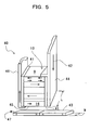
- Fig. 5 is a conceptual diagram illustrating a magnetic head according to a fourth form of implementation of the present invention.
- a magnetic head 40 comprises a CPP type giant magnetoresistance device 10, and a first and a second electrode 44 and 46.
- the CPP-GMR device 10 is shown having an antiferromagnetic layer 9 and a SyAF with a second magnetic layer 16 and has two opposite ends covered with insulating layers 41 and 41.
- the first electrode 44 is designed to supply spin dependent sensor electrons 42 from the antiferromagnetic layer 9 and also serves as a magnetic shield.
- the second electrode 46 is disposed in contact with an end face 45 of the second magnetic layer 16 in the SyAF to serve as a magnetic shield, too.
- a recording medium 43 such as a magnetic disk lies opposed to the end face 45 of the second magnetic layer 16 in the SyAF side of the CCP type giant magnetoresistance device.
- the insulating layers 41 and 41 may be such as to control the conduction path of sensor electrons to permit their conduction in a direction perpendicular to film planes.
- the first and second electrodes 44 and 46 of the magnetic head 40 should satisfactorily be not less than the width of the CPP type giant magnetoresistance device and it is satisfactory at least if the magnetic head has a width L that is not more than the track width W of the recording medium.
- the arrow 47 in Fig. 5 indicates the direction in which the recording medium is moved.
- the magnetic head 40 so constructed as mentioned above will have the SyAF caused to reverse its magnetizations in response to a leakage magnetic field from the recording medium to bring about CPP-GMR based on the spin dependent scatterings of sensor electrons and will have its electrical resistance varied thereby.
- the magnetic head according to this form of implementation of the invention allows detecting the direction of a magnetic field from the recording medium as a change in electrical resistance. Further, since a magnetic field to be shielded is confined to its width or so, the magnetic head can achieve magnetic shielding even if the recording medium is highly densified.
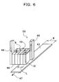
- FIG. 6 is a conceptual diagram illustrating another form of implementation of the magnetic head.
- a magnetic head 50 shown in Fig. 6 is of the form in which a stratal face 48 of the CPP type giant magnetoresistance device 10, 20, 25 on which its multi-layered structure appears is set face to face with a recording medium 43. It has a first electrode 44 formed in contact with a whole or part surface of the end face of the antiferromagnetic layer 9 and a second electrode 46 formed in contact with a whole or part surface of the end face of the second magnetic layer 16 in the SyAF.
- magnetic shield layers via insulating layers as shown in connection with the second form of implementation may be provided.
- the first and second electrodes 44 and 46 should be insulated from each other.
- These magnetic shields may each be of any form if it can magnetically shield the SyAF.
- the magnetic head so constructed makes it possible to detect a magnetic field from the recording medium having a track width W of a size of the width L of the SyAF and can make reproductions even from a highly densified recording medium.
- a CPP type giant magnetoresistance device can widely be utilized in what can be called magnetic components such as a field sensor, an angle sensor and an angular displacement sensor.
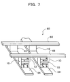
- Fig. 7 is a conceptual diagram illustrating a magnetic recorder capable of storing information to which a CPP type giant magnetoresistance device of the invention is applied.
- Fig. 7 there is shown a structure in which a CPP type giant magnetoresistance device 10, 20, 25 is disposed at each of intersections of word lines 64 and bit lines 66. Since the magnetic field which the SyAF 13 of the invention requires to reverse its magnetizations is extremely small, passing an electric current of several milliamperes or so, e. g., 5 mA, for spin injection is sufficient to cause the SyAF 13 to reverse its magnetizations.
- writing is performed by selecting a CPP type giant magnetoresistance device from a combination of a word and a bit lines and passing an electric current, e. g., of 5 mA, from the word line for spin injection to reverse magnetizations of the SyAF therein.
- an electric current e. g., of 5 mA
- a CPP type giant magnetoresistance device is selected and from its word line an electric current of, e. g., 1 mA, that is smaller than that required for writing is passed to develop CPP-GMR by spin dependent electron scattering and then to determine a change in resistance of the CPP type magnetoresistance device or whether the resistance is large or small.
- information units "1" and "0" can be determined depending on whether the fixed and free layers are magnetized parallel and antiparallel to each other, and causing the free layer to remain magnetized after the current supply is cut off allows forming a MRAM as a nonvolatile memory.
- Fig. 8 is a diagrammatic view illustrating a CPP type giant magnetoresistance device according to the first form of implementation of the invention and a four terminal technique used to determine its properties.
- a CPP-GMR structure corresponding to that shown in Fig. 1.
- Fig. 1 As shown in Fig.
- a thermally oxidized silicon substrate 51 has a lower electrode 52 and a lower, highly conductive layer 53 laid thereon, and mounted on the latter the first Example has a CPP-GMR structure 58 in which are successively multi-layered a CPP type magnetoresistance device 10 as a multi-layered structure of an antiferromagnetic layer, a ferromagnetic fixed layer, a nonmagnetic conductive layer and SyAF, an upper electrode 54 and an upper highly conductive layer 55.
- the first Example is further provided with insulating layers 56 and 56 for insulating the CPP-GMR structure 58, a voltmeter 57 for sensing a signal voltage, a first electrode 59, a power supply 61 for supplying sense electrons and a second electrode 62.
- the CPP-GMR structure 58 was prepared as stated below.
- the thermally oxidized Si substrate had successively multi-layered thereon, Ta (10 nm), Cu (2.5 nm), IrMn (10 nm), Co 90 Fe 10 (3 nm), Cu (2.5 nm), Co 90 Fe 10 (5 nm), Ru (0.45 nm), Co 90 Fe 10 (3 nm) and Ta (5 nm).
- film thicknesses are indicated in parentheses.
- Lower Ta (10 nm), IrMn and upper Ta (5 nm) form the lower electrode, the antiferromagnetic layer and the upper electrode, respectively.
- Co 90 Fe 10 (5 nm), Ru (0.45 nm) and Co 90 Fe 10 (3nm) form the SyAF in which Ru magnetically couples two Co 90 Fe 10 magnetic layers together antiparallel to each other.
- the Co 90 Fe 10 (3 nm) in contact with IrMn has spins fixed therein, thus constituting the fixed layer.
- a second Example was performed in which as in the first Example, films of Ta (10 nm), Cu (20 nm), IrMn (10 nm), Co 90 Fe 10 (3 nm), Cu (6 nm), Co 90 Fe 10 (3 nm), Ru (0.45 nm), Co 90 Fe 10 (5 nm), Ta (3 nm) and Cu (50 nm) were formed on a thermally oxidized Si substrate.
- the comparative example was carried out in the same way as the first Example except that Co 90 Fe 10 (3 nm), Ru (0.45 nm) and Co 90 Fe 10 (5 nm) were replaced by Co 90 Fe 10 (8 nm) to prepare a conventional CPP-GMR device.
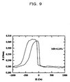
- the CPP-GMR was measured and determined to be 0.5 %, which amounts to 1/10 or less of the value in the first Example.
- the present invention provides a CPP type giant magnetoresistance device which is extremely large in CPP-GMR and hence can be used to detect the direction of a magnetic field such as from a recording medium as a large change in electrical resistance and can be applied to what are called magnetic components such as a magnetic field sensor, an angle sensor and an angular displacement sensor.
- the present invention further provides a magnetic device or unit which, having the capability of writing or reading upon passing spin dependent current while having nonvolatile magnetic storage capability, can be used in a variety of types of magnetic recorders such as a digital VTR and a hard disk drive (HDD), and also in a MRAM.
- a magnetic device or unit which, having the capability of writing or reading upon passing spin dependent current while having nonvolatile magnetic storage capability, can be used in a variety of types of magnetic recorders such as a digital VTR and a hard disk drive (HDD), and also in a MRAM.
Landscapes
- Engineering & Computer Science (AREA)
- Chemical & Material Sciences (AREA)
- Nanotechnology (AREA)
- Physics & Mathematics (AREA)
- Crystallography & Structural Chemistry (AREA)
- Power Engineering (AREA)
- General Physics & Mathematics (AREA)
- Computer Hardware Design (AREA)
- Condensed Matter Physics & Semiconductors (AREA)
- Mathematical Physics (AREA)
- Theoretical Computer Science (AREA)
- Hall/Mr Elements (AREA)
- Magnetic Heads (AREA)
- Thin Magnetic Films (AREA)
- Semiconductor Memories (AREA)
- Measuring Magnetic Variables (AREA)
- Mram Or Spin Memory Techniques (AREA)
Priority Applications (1)
| Application Number | Priority Date | Filing Date | Title |
|---|---|---|---|
| EP10011433.9A EP2267811B1 (de) | 2003-01-31 | 2004-01-23 | Riesenmagnetowiderstandseffektelement vom CPP-Typ und magnetisches Bauelement und magnetische Vorrichtung, die es benutzen |
Applications Claiming Priority (5)
| Application Number | Priority Date | Filing Date | Title |
|---|---|---|---|
| JP2003024981 | 2003-01-31 | ||
| JP2003024981 | 2003-01-31 | ||
| JP2003137945 | 2003-05-15 | ||
| JP2003137945A JP2004289100A (ja) | 2003-01-31 | 2003-05-15 | Cpp型巨大磁気抵抗素子及びそれを用いた磁気部品並びに磁気装置 |
| PCT/JP2004/000594 WO2004068607A1 (ja) | 2003-01-31 | 2004-01-23 | Cpp型巨大磁気抵抗素子及びそれを用いた磁気部品並びに磁気装置 |
Related Child Applications (1)
| Application Number | Title | Priority Date | Filing Date |
|---|---|---|---|
| EP10011433.9 Division-Into | 2010-09-29 |
Publications (3)
| Publication Number | Publication Date |
|---|---|
| EP1589594A1 true EP1589594A1 (de) | 2005-10-26 |
| EP1589594A4 EP1589594A4 (de) | 2006-06-14 |
| EP1589594B1 EP1589594B1 (de) | 2013-06-19 |
Family
ID=32828933
Family Applications (2)
| Application Number | Title | Priority Date | Filing Date |
|---|---|---|---|
| EP10011433.9A Expired - Lifetime EP2267811B1 (de) | 2003-01-31 | 2004-01-23 | Riesenmagnetowiderstandseffektelement vom CPP-Typ und magnetisches Bauelement und magnetische Vorrichtung, die es benutzen |
| EP04704713.9A Expired - Lifetime EP1589594B1 (de) | 2003-01-31 | 2004-01-23 | Riesen-magnetowiderstandseffektelement des ccp-typs und magnetische komponente und magnetische einrichtung damit |
Family Applications Before (1)
| Application Number | Title | Priority Date | Filing Date |
|---|---|---|---|
| EP10011433.9A Expired - Lifetime EP2267811B1 (de) | 2003-01-31 | 2004-01-23 | Riesenmagnetowiderstandseffektelement vom CPP-Typ und magnetisches Bauelement und magnetische Vorrichtung, die es benutzen |
Country Status (5)
| Country | Link |
|---|---|
| US (1) | US7385790B2 (de) |
| EP (2) | EP2267811B1 (de) |
| JP (1) | JP2004289100A (de) |
| KR (1) | KR100713089B1 (de) |
| WO (1) | WO2004068607A1 (de) |
Families Citing this family (19)
| Publication number | Priority date | Publication date | Assignee | Title |
|---|---|---|---|---|
| JP2006165059A (ja) * | 2004-12-02 | 2006-06-22 | Sony Corp | 記憶素子及びメモリ |
| JP2006196613A (ja) * | 2005-01-12 | 2006-07-27 | Sony Corp | 記憶素子及びその製造方法、メモリ |
| US7355823B2 (en) * | 2005-01-26 | 2008-04-08 | Head Way Technologies, Inc. | Ta based bilayer seed for IrMn CPP spin valve |
| JP4756868B2 (ja) * | 2005-01-31 | 2011-08-24 | キヤノン株式会社 | 検出方法 |
| JP4731927B2 (ja) * | 2005-01-31 | 2011-07-27 | キヤノン株式会社 | 磁性体センサおよび検出キット |
| JP4508058B2 (ja) * | 2005-09-26 | 2010-07-21 | 三菱電機株式会社 | 磁界検出装置およびその製造方法 |
| US7745893B2 (en) * | 2005-10-17 | 2010-06-29 | Northern Lights Semiconductor Corp. | Magnetic transistor structure |
| JP4444241B2 (ja) * | 2005-10-19 | 2010-03-31 | 株式会社東芝 | 磁気抵抗効果素子、磁気ランダムアクセスメモリ、電子カード及び電子装置 |
| JP5376880B2 (ja) * | 2007-09-27 | 2013-12-25 | 株式会社東芝 | 磁気記録ヘッド及び磁気記録装置 |
| JP5036585B2 (ja) * | 2008-02-13 | 2012-09-26 | 株式会社東芝 | 磁性発振素子、この磁性発振素子を有する磁気ヘッド、および磁気記録再生装置 |
| JP5408895B2 (ja) * | 2008-04-15 | 2014-02-05 | キヤノン株式会社 | 物質検出装置、及び、該物質検出装置を用いた物質検出方法 |
| JP2009031303A (ja) * | 2008-09-22 | 2009-02-12 | Canon Inc | 検出デバイス及び検出用キット |
| US20110026169A1 (en) * | 2009-07-28 | 2011-02-03 | Hardayal Singh Gill | Dual cpp gmr head using a scissor sensor |
| KR101598831B1 (ko) | 2009-10-14 | 2016-03-03 | 삼성전자주식회사 | 자기저항소자, 이를 포함하는 정보저장장치 및 상기 정보저장장치의 동작방법 |
| US8705213B2 (en) * | 2010-02-26 | 2014-04-22 | Seagate Technology Llc | Magnetic field detecting device with shielding layer at least partially surrounding magnetoresistive stack |
| CN102901940B (zh) | 2012-10-26 | 2015-07-15 | 苏州大学 | 基于磁温差电效应的传感器元件及其实现方法 |
| KR101827294B1 (ko) * | 2013-10-31 | 2018-02-08 | 고쿠리츠켄큐카이하츠호진 카가쿠기쥬츠신코키코 | 스핀 제어 기구 및 스핀 디바이스 |
| EP3235018A4 (de) * | 2014-12-18 | 2018-08-15 | Intel Corporation | Verfahren zur herstellung von logischen spin-vorrichtungen aus in-situ-abgeschiedenen magnetischen stapeln |
| US10755733B1 (en) | 2019-03-05 | 2020-08-25 | Sandisk Technologies Llc | Read head including semiconductor spacer and long spin diffusion length nonmagnetic conductive material and method of making thereof |
Family Cites Families (24)
| Publication number | Priority date | Publication date | Assignee | Title |
|---|---|---|---|---|
| US5583725A (en) * | 1994-06-15 | 1996-12-10 | International Business Machines Corporation | Spin valve magnetoresistive sensor with self-pinned laminated layer and magnetic recording system using the sensor |
| JP3691898B2 (ja) | 1996-03-18 | 2005-09-07 | 株式会社東芝 | 磁気抵抗効果素子、磁気情報読み出し方法、及び記録素子 |
| JP4066477B2 (ja) * | 1997-10-09 | 2008-03-26 | ソニー株式会社 | 不揮発性ランダムアクセスメモリー装置 |
| US6052263A (en) * | 1998-08-21 | 2000-04-18 | International Business Machines Corporation | Low moment/high coercivity pinned layer for magnetic tunnel junction sensors |
| US6567246B1 (en) * | 1999-03-02 | 2003-05-20 | Matsushita Electric Industrial Co., Ltd. | Magnetoresistance effect element and method for producing the same, and magnetoresistance effect type head, magnetic recording apparatus, and magnetoresistance effect memory element |
| US6611405B1 (en) * | 1999-09-16 | 2003-08-26 | Kabushiki Kaisha Toshiba | Magnetoresistive element and magnetic memory device |
| US6271997B1 (en) * | 1999-11-22 | 2001-08-07 | International Business Machines Corporation | Read head spin valve sensor with triple antiparallel coupled free layer structure |
| US6445552B1 (en) * | 2000-02-18 | 2002-09-03 | International Business Machines Corporation | Shield design for stable magnetoresistive head |
| US6517896B1 (en) | 2000-08-07 | 2003-02-11 | Headway Technologies, Inc. | Spin filter bottom spin valve head with continuous spacer exchange bias |
| JP2002092829A (ja) * | 2000-09-21 | 2002-03-29 | Fujitsu Ltd | 磁気抵抗センサ及び磁気抵抗ヘッド |
| JP4092867B2 (ja) | 2000-10-16 | 2008-05-28 | セイコーエプソン株式会社 | 圧電体膜及びこれを備えた圧電体素子 |
| US6893734B2 (en) * | 2000-12-22 | 2005-05-17 | Alps Electric Co., Ltd. | Magnetic sensing element with improved sensitivity and method for making the same |
| JP3889276B2 (ja) * | 2000-12-22 | 2007-03-07 | アルプス電気株式会社 | 磁気検出素子 |
| TW544677B (en) * | 2000-12-26 | 2003-08-01 | Matsushita Electric Industrial Co Ltd | Magneto-resistance memory device |
| US6992869B2 (en) * | 2001-02-06 | 2006-01-31 | Yamaha Corporation | Magnetic resistance device |
| JP3939514B2 (ja) * | 2001-03-27 | 2007-07-04 | アルプス電気株式会社 | 磁気検出素子の製造方法 |
| JP3849460B2 (ja) * | 2001-05-29 | 2006-11-22 | ソニー株式会社 | 磁気抵抗効果素子、磁気抵抗効果型磁気センサ、および磁気抵抗効果型磁気ヘッド |
| JP2002359415A (ja) | 2001-05-31 | 2002-12-13 | Sony Corp | 面垂直電流型磁気抵抗効果素子、その製造方法、再生ヘッド、及びこれを搭載した情報記憶装置 |
| JP3563375B2 (ja) * | 2001-06-19 | 2004-09-08 | アルプス電気株式会社 | 磁気検出素子及び前記磁気検出素子を用いた薄膜磁気ヘッド |
| JP3565268B2 (ja) * | 2001-06-22 | 2004-09-15 | 株式会社東芝 | 磁気抵抗効果素子、磁気ヘッド及び磁気再生装置 |
| JP3590006B2 (ja) * | 2001-06-22 | 2004-11-17 | 株式会社東芝 | 磁気抵抗効果素子、磁気ヘッド及び磁気再生装置 |
| JP4184668B2 (ja) * | 2002-01-10 | 2008-11-19 | 富士通株式会社 | Cpp構造磁気抵抗効果素子 |
| JP3657571B2 (ja) * | 2002-03-28 | 2005-06-08 | 株式会社東芝 | 磁気抵抗効果素子、磁気ヘッド及び磁気再生装置 |
| US6876527B2 (en) * | 2002-11-08 | 2005-04-05 | Hitachi Global Storage Technologies Netherlands B.V. | Magnetoresistive sensor with antiparallel coupled lead/sensor overlap region |
-
2003
- 2003-05-15 JP JP2003137945A patent/JP2004289100A/ja active Pending
-
2004
- 2004-01-23 EP EP10011433.9A patent/EP2267811B1/de not_active Expired - Lifetime
- 2004-01-23 US US10/544,007 patent/US7385790B2/en not_active Expired - Fee Related
- 2004-01-23 WO PCT/JP2004/000594 patent/WO2004068607A1/ja not_active Ceased
- 2004-01-23 KR KR1020057014057A patent/KR100713089B1/ko not_active Expired - Fee Related
- 2004-01-23 EP EP04704713.9A patent/EP1589594B1/de not_active Expired - Lifetime
Also Published As
| Publication number | Publication date |
|---|---|
| WO2004068607A1 (ja) | 2004-08-12 |
| US20060139817A1 (en) | 2006-06-29 |
| KR20050095881A (ko) | 2005-10-04 |
| KR100713089B1 (ko) | 2007-05-02 |
| EP2267811A2 (de) | 2010-12-29 |
| EP1589594B1 (de) | 2013-06-19 |
| JP2004289100A (ja) | 2004-10-14 |
| EP1589594A4 (de) | 2006-06-14 |
| EP2267811A3 (de) | 2011-03-30 |
| US7385790B2 (en) | 2008-06-10 |
| EP2267811B1 (de) | 2013-08-28 |
Similar Documents
| Publication | Publication Date | Title |
|---|---|---|
| US7502208B2 (en) | Magneto-resistive effect element, magnetic sensor using magneto-resistive effect, magnetic head using magneto-resistive effect and magnetic memory | |
| US7385790B2 (en) | CPP-type giant manetoresistance effect element and magnetic component and magnetic device using it | |
| JP3589346B2 (ja) | 磁気抵抗効果素子および磁気抵抗効果記憶素子 | |
| US7035062B1 (en) | Structure to achieve sensitivity and linear density in tunneling GMR heads using orthogonal magnetic alignments | |
| US7016161B2 (en) | Magnetic head, magnetic head gimbal assembly, magnetic recording and reproducing apparatus, and magnetic memory | |
| US5159513A (en) | Magnetoresistive sensor based on the spin valve effect | |
| US6947264B2 (en) | Self-pinned in-stack bias structure for magnetoresistive read heads | |
| JP3849460B2 (ja) | 磁気抵抗効果素子、磁気抵抗効果型磁気センサ、および磁気抵抗効果型磁気ヘッド | |
| KR100265983B1 (ko) | 박막자기헤드 | |
| JP4088641B2 (ja) | 磁気抵抗効果素子、薄膜磁気ヘッド、ヘッドジンバルアセンブリ、ヘッドアームアセンブリ、磁気ディスク装置、磁気メモリセルおよび電流センサ | |
| JP2004260149A (ja) | 固定層に半金属強磁性体ホイスラー合金を有する交換結合構造の磁気抵抗素子 | |
| GB2387711A (en) | Magnetic sensing element with multi-layer free layer | |
| JP2002150512A (ja) | 磁気抵抗効果素子および磁気抵抗効果型磁気ヘッド | |
| US6621666B2 (en) | Magnetoresistive-effect element having electrode layers oppositely disposed on main surfaces of a magnetoresistive-effect thin film having hard magnetic bias layers with a particular resistivity | |
| US6654209B2 (en) | Low resistance lead structure for a low resistance magnetic read head | |
| KR20010075693A (ko) | 자기 스위치 자계가 감소된 자기저항 센서 또는 메모리 소자 | |
| JPH07297465A (ja) | 絶縁ピン留め層を備えた巨大磁気抵抗センサ | |
| JP2002270922A (ja) | 磁気抵抗素子 | |
| US8295015B2 (en) | Magnetoresistive element, thin film magnetic head, magnetic head slider, head gimbal assembly, head arm assembly and magnetic disk device | |
| US7948717B2 (en) | Magneto-resistance effect element, magnetic head, magnetic recording/reproducing device and magnetic memory | |
| US7961441B2 (en) | Exchange coupled film including hafnium and amorphous layers usable in a magnetoresistive element in a thin-film magnetic head | |
| JP2008090877A (ja) | 磁気ヘッド及び磁気記録装置 | |
| JP2002353533A (ja) | 磁気抵抗効果素子、磁気抵抗効果型磁気センサ、磁気抵抗効果型磁気ヘッド、および磁気メモリ | |
| JP2000182224A (ja) | 高い熱安定性を有するスピン・バルブ読取りセンサ及びその製造方法 | |
| JP2005191577A (ja) | 磁気抵抗効果素子、磁気抵抗効果ヘッド、磁気抵抗変換システム及び磁気記録システム |
Legal Events
| Date | Code | Title | Description |
|---|---|---|---|
| PUAI | Public reference made under article 153(3) epc to a published international application that has entered the european phase |
Free format text: ORIGINAL CODE: 0009012 |
|
| 17P | Request for examination filed |
Effective date: 20050722 |
|
| AK | Designated contracting states |
Kind code of ref document: A1 Designated state(s): AT BE BG CH CY CZ DE DK EE ES FI FR GB GR HU IE IT LI LU MC NL PT RO SE SI SK TR |
|
| AX | Request for extension of the european patent |
Extension state: AL LT LV MK |
|
| DAX | Request for extension of the european patent (deleted) | ||
| RBV | Designated contracting states (corrected) |
Designated state(s): DE FR NL |
|
| A4 | Supplementary search report drawn up and despatched |
Effective date: 20060503 |
|
| 17Q | First examination report despatched |
Effective date: 20070125 |
|
| RIN1 | Information on inventor provided before grant (corrected) |
Inventor name: INOMATA, KOUICHIRO Inventor name: TEZUKA, NOBUKI |
|
| REG | Reference to a national code |
Ref country code: DE Ref legal event code: R079 Ref document number: 602004042463 Country of ref document: DE Free format text: PREVIOUS MAIN CLASS: H01L0043080000 Ipc: G01R0033090000 |
|
| RIC1 | Information provided on ipc code assigned before grant |
Ipc: B82Y 25/00 20110101ALI20120719BHEP Ipc: H01L 27/22 20060101ALI20120719BHEP Ipc: G11C 11/15 20060101ALI20120719BHEP Ipc: G01R 33/09 20060101AFI20120719BHEP Ipc: B82Y 10/00 20110101ALI20120719BHEP Ipc: H01F 10/32 20060101ALI20120719BHEP Ipc: H01L 43/08 20060101ALI20120719BHEP |
|
| GRAP | Despatch of communication of intention to grant a patent |
Free format text: ORIGINAL CODE: EPIDOSNIGR1 |
|
| RIN1 | Information on inventor provided before grant (corrected) |
Inventor name: TEZUKA, NOBUKI Inventor name: INOMATA, KOUICHIRO |
|
| GRAS | Grant fee paid |
Free format text: ORIGINAL CODE: EPIDOSNIGR3 |
|
| GRAP | Despatch of communication of intention to grant a patent |
Free format text: ORIGINAL CODE: EPIDOSNIGR1 |
|
| GRAA | (expected) grant |
Free format text: ORIGINAL CODE: 0009210 |
|
| AK | Designated contracting states |
Kind code of ref document: B1 Designated state(s): DE FR NL |
|
| REG | Reference to a national code |
Ref country code: DE Ref legal event code: R096 Ref document number: 602004042463 Country of ref document: DE Effective date: 20130808 |
|
| REG | Reference to a national code |
Ref country code: NL Ref legal event code: T3 |
|
| PLBE | No opposition filed within time limit |
Free format text: ORIGINAL CODE: 0009261 |
|
| STAA | Information on the status of an ep patent application or granted ep patent |
Free format text: STATUS: NO OPPOSITION FILED WITHIN TIME LIMIT |
|
| 26N | No opposition filed |
Effective date: 20140320 |
|
| REG | Reference to a national code |
Ref country code: DE Ref legal event code: R097 Ref document number: 602004042463 Country of ref document: DE Effective date: 20140320 |
|
| REG | Reference to a national code |
Ref country code: FR Ref legal event code: PLFP Year of fee payment: 13 |
|
| REG | Reference to a national code |
Ref country code: FR Ref legal event code: PLFP Year of fee payment: 14 |
|
| PGFP | Annual fee paid to national office [announced via postgrant information from national office to epo] |
Ref country code: NL Payment date: 20161207 Year of fee payment: 14 |
|
| PGFP | Annual fee paid to national office [announced via postgrant information from national office to epo] |
Ref country code: FR Payment date: 20161213 Year of fee payment: 14 |
|
| PGFP | Annual fee paid to national office [announced via postgrant information from national office to epo] |
Ref country code: DE Payment date: 20161207 Year of fee payment: 14 |
|
| REG | Reference to a national code |
Ref country code: DE Ref legal event code: R119 Ref document number: 602004042463 Country of ref document: DE |
|
| REG | Reference to a national code |
Ref country code: NL Ref legal event code: MM Effective date: 20180201 |
|
| PG25 | Lapsed in a contracting state [announced via postgrant information from national office to epo] |
Ref country code: DE Free format text: LAPSE BECAUSE OF NON-PAYMENT OF DUE FEES Effective date: 20180801 Ref country code: FR Free format text: LAPSE BECAUSE OF NON-PAYMENT OF DUE FEES Effective date: 20180131 |
|
| REG | Reference to a national code |
Ref country code: FR Ref legal event code: ST Effective date: 20180928 |
|
| PG25 | Lapsed in a contracting state [announced via postgrant information from national office to epo] |
Ref country code: NL Free format text: LAPSE BECAUSE OF NON-PAYMENT OF DUE FEES Effective date: 20180201 |