EP1587183A1 - Gegenstand mit eingegossenem Einsatz und Herstellungsverfahren - Google Patents
Gegenstand mit eingegossenem Einsatz und Herstellungsverfahren Download PDFInfo
- Publication number
- EP1587183A1 EP1587183A1 EP05007684A EP05007684A EP1587183A1 EP 1587183 A1 EP1587183 A1 EP 1587183A1 EP 05007684 A EP05007684 A EP 05007684A EP 05007684 A EP05007684 A EP 05007684A EP 1587183 A1 EP1587183 A1 EP 1587183A1
- Authority
- EP
- European Patent Office
- Prior art keywords
- insert
- casing
- mold
- interlocking portion
- molded article
- Prior art date
- Legal status (The legal status is an assumption and is not a legal conclusion. Google has not performed a legal analysis and makes no representation as to the accuracy of the status listed.)
- Granted
Links
Images

Classifications
-
- H—ELECTRICITY
- H01—ELECTRIC ELEMENTS
- H01R—ELECTRICALLY-CONDUCTIVE CONNECTIONS; STRUCTURAL ASSOCIATIONS OF A PLURALITY OF MUTUALLY-INSULATED ELECTRICAL CONNECTING ELEMENTS; COUPLING DEVICES; CURRENT COLLECTORS
- H01R43/00—Apparatus or processes specially adapted for manufacturing, assembling, maintaining, or repairing of line connectors or current collectors or for joining electric conductors
- H01R43/20—Apparatus or processes specially adapted for manufacturing, assembling, maintaining, or repairing of line connectors or current collectors or for joining electric conductors for assembling or disassembling contact members with insulating base, case or sleeve
- H01R43/24—Assembling by moulding on contact members
-
- B—PERFORMING OPERATIONS; TRANSPORTING
- B29—WORKING OF PLASTICS; WORKING OF SUBSTANCES IN A PLASTIC STATE IN GENERAL
- B29C—SHAPING OR JOINING OF PLASTICS; SHAPING OF MATERIAL IN A PLASTIC STATE, NOT OTHERWISE PROVIDED FOR; AFTER-TREATMENT OF THE SHAPED PRODUCTS, e.g. REPAIRING
- B29C45/00—Injection moulding, i.e. forcing the required volume of moulding material through a nozzle into a closed mould; Apparatus therefor
- B29C45/14—Injection moulding, i.e. forcing the required volume of moulding material through a nozzle into a closed mould; Apparatus therefor incorporating preformed parts or layers, e.g. injection moulding around inserts or for coating articles
- B29C45/14065—Positioning or centering articles in the mould
-
- B—PERFORMING OPERATIONS; TRANSPORTING
- B29—WORKING OF PLASTICS; WORKING OF SUBSTANCES IN A PLASTIC STATE IN GENERAL
- B29C—SHAPING OR JOINING OF PLASTICS; SHAPING OF MATERIAL IN A PLASTIC STATE, NOT OTHERWISE PROVIDED FOR; AFTER-TREATMENT OF THE SHAPED PRODUCTS, e.g. REPAIRING
- B29C45/00—Injection moulding, i.e. forcing the required volume of moulding material through a nozzle into a closed mould; Apparatus therefor
- B29C45/14—Injection moulding, i.e. forcing the required volume of moulding material through a nozzle into a closed mould; Apparatus therefor incorporating preformed parts or layers, e.g. injection moulding around inserts or for coating articles
- B29C45/14336—Coating a portion of the article, e.g. the edge of the article
- B29C45/14377—Coating a portion of the article, e.g. the edge of the article using an additional insert, e.g. a fastening element
-
- B—PERFORMING OPERATIONS; TRANSPORTING
- B29—WORKING OF PLASTICS; WORKING OF SUBSTANCES IN A PLASTIC STATE IN GENERAL
- B29C—SHAPING OR JOINING OF PLASTICS; SHAPING OF MATERIAL IN A PLASTIC STATE, NOT OTHERWISE PROVIDED FOR; AFTER-TREATMENT OF THE SHAPED PRODUCTS, e.g. REPAIRING
- B29C45/00—Injection moulding, i.e. forcing the required volume of moulding material through a nozzle into a closed mould; Apparatus therefor
- B29C45/14—Injection moulding, i.e. forcing the required volume of moulding material through a nozzle into a closed mould; Apparatus therefor incorporating preformed parts or layers, e.g. injection moulding around inserts or for coating articles
- B29C45/14639—Injection moulding, i.e. forcing the required volume of moulding material through a nozzle into a closed mould; Apparatus therefor incorporating preformed parts or layers, e.g. injection moulding around inserts or for coating articles for obtaining an insulating effect, e.g. for electrical components
-
- H—ELECTRICITY
- H05—ELECTRIC TECHNIQUES NOT OTHERWISE PROVIDED FOR
- H05K—PRINTED CIRCUITS; CASINGS OR CONSTRUCTIONAL DETAILS OF ELECTRIC APPARATUS; MANUFACTURE OF ASSEMBLAGES OF ELECTRICAL COMPONENTS
- H05K3/00—Apparatus or processes for manufacturing printed circuits
- H05K3/0058—Laminating printed circuit boards onto other substrates, e.g. metallic substrates
-
- B—PERFORMING OPERATIONS; TRANSPORTING
- B29—WORKING OF PLASTICS; WORKING OF SUBSTANCES IN A PLASTIC STATE IN GENERAL
- B29C—SHAPING OR JOINING OF PLASTICS; SHAPING OF MATERIAL IN A PLASTIC STATE, NOT OTHERWISE PROVIDED FOR; AFTER-TREATMENT OF THE SHAPED PRODUCTS, e.g. REPAIRING
- B29C45/00—Injection moulding, i.e. forcing the required volume of moulding material through a nozzle into a closed mould; Apparatus therefor
- B29C45/14—Injection moulding, i.e. forcing the required volume of moulding material through a nozzle into a closed mould; Apparatus therefor incorporating preformed parts or layers, e.g. injection moulding around inserts or for coating articles
- B29C45/14065—Positioning or centering articles in the mould
- B29C2045/14131—Positioning or centering articles in the mould using positioning or centering means forming part of the insert
-
- B—PERFORMING OPERATIONS; TRANSPORTING
- B29—WORKING OF PLASTICS; WORKING OF SUBSTANCES IN A PLASTIC STATE IN GENERAL
- B29C—SHAPING OR JOINING OF PLASTICS; SHAPING OF MATERIAL IN A PLASTIC STATE, NOT OTHERWISE PROVIDED FOR; AFTER-TREATMENT OF THE SHAPED PRODUCTS, e.g. REPAIRING
- B29C45/00—Injection moulding, i.e. forcing the required volume of moulding material through a nozzle into a closed mould; Apparatus therefor
- B29C45/16—Making multilayered or multicoloured articles
- B29C45/1671—Making multilayered or multicoloured articles with an insert
-
- H—ELECTRICITY
- H05—ELECTRIC TECHNIQUES NOT OTHERWISE PROVIDED FOR
- H05K—PRINTED CIRCUITS; CASINGS OR CONSTRUCTIONAL DETAILS OF ELECTRIC APPARATUS; MANUFACTURE OF ASSEMBLAGES OF ELECTRICAL COMPONENTS
- H05K2201/00—Indexing scheme relating to printed circuits covered by H05K1/00
- H05K2201/09—Shape and layout
- H05K2201/09009—Substrate related
- H05K2201/09118—Moulded substrate
-
- H—ELECTRICITY
- H05—ELECTRIC TECHNIQUES NOT OTHERWISE PROVIDED FOR
- H05K—PRINTED CIRCUITS; CASINGS OR CONSTRUCTIONAL DETAILS OF ELECTRIC APPARATUS; MANUFACTURE OF ASSEMBLAGES OF ELECTRICAL COMPONENTS
- H05K2203/00—Indexing scheme relating to apparatus or processes for manufacturing printed circuits covered by H05K3/00
- H05K2203/13—Moulding and encapsulation; Deposition techniques; Protective layers
- H05K2203/1305—Moulding and encapsulation
- H05K2203/1327—Moulding over PCB locally or completely
-
- H—ELECTRICITY
- H05—ELECTRIC TECHNIQUES NOT OTHERWISE PROVIDED FOR
- H05K—PRINTED CIRCUITS; CASINGS OR CONSTRUCTIONAL DETAILS OF ELECTRIC APPARATUS; MANUFACTURE OF ASSEMBLAGES OF ELECTRICAL COMPONENTS
- H05K3/00—Apparatus or processes for manufacturing printed circuits
- H05K3/10—Apparatus or processes for manufacturing printed circuits in which conductive material is applied to the insulating support in such a manner as to form the desired conductive pattern
- H05K3/20—Apparatus or processes for manufacturing printed circuits in which conductive material is applied to the insulating support in such a manner as to form the desired conductive pattern by affixing prefabricated conductor pattern
- H05K3/202—Apparatus or processes for manufacturing printed circuits in which conductive material is applied to the insulating support in such a manner as to form the desired conductive pattern by affixing prefabricated conductor pattern using self-supporting metal foil pattern
-
- Y—GENERAL TAGGING OF NEW TECHNOLOGICAL DEVELOPMENTS; GENERAL TAGGING OF CROSS-SECTIONAL TECHNOLOGIES SPANNING OVER SEVERAL SECTIONS OF THE IPC; TECHNICAL SUBJECTS COVERED BY FORMER USPC CROSS-REFERENCE ART COLLECTIONS [XRACs] AND DIGESTS
- Y10—TECHNICAL SUBJECTS COVERED BY FORMER USPC
- Y10T—TECHNICAL SUBJECTS COVERED BY FORMER US CLASSIFICATION
- Y10T428/00—Stock material or miscellaneous articles
- Y10T428/22—Nonparticulate element embedded or inlaid in substrate and visible
-
- Y—GENERAL TAGGING OF NEW TECHNOLOGICAL DEVELOPMENTS; GENERAL TAGGING OF CROSS-SECTIONAL TECHNOLOGIES SPANNING OVER SEVERAL SECTIONS OF THE IPC; TECHNICAL SUBJECTS COVERED BY FORMER USPC CROSS-REFERENCE ART COLLECTIONS [XRACs] AND DIGESTS
- Y10—TECHNICAL SUBJECTS COVERED BY FORMER USPC
- Y10T—TECHNICAL SUBJECTS COVERED BY FORMER US CLASSIFICATION
- Y10T428/00—Stock material or miscellaneous articles
- Y10T428/23—Sheet including cover or casing
-
- Y—GENERAL TAGGING OF NEW TECHNOLOGICAL DEVELOPMENTS; GENERAL TAGGING OF CROSS-SECTIONAL TECHNOLOGIES SPANNING OVER SEVERAL SECTIONS OF THE IPC; TECHNICAL SUBJECTS COVERED BY FORMER USPC CROSS-REFERENCE ART COLLECTIONS [XRACs] AND DIGESTS
- Y10—TECHNICAL SUBJECTS COVERED BY FORMER USPC
- Y10T—TECHNICAL SUBJECTS COVERED BY FORMER US CLASSIFICATION
- Y10T428/00—Stock material or miscellaneous articles
- Y10T428/24—Structurally defined web or sheet [e.g., overall dimension, etc.]
- Y10T428/24479—Structurally defined web or sheet [e.g., overall dimension, etc.] including variation in thickness
- Y10T428/24612—Composite web or sheet
Definitions
- the present invention relates to an insert-molded article and a production method for insert-molded article.
- the present invention was developed in view of the above problem and an object thereof is to improve operability, in particular ensure watertightness.
- an insert-molded article provided with a casing formed by insert molding using an inner portion holding at least one insert member, preferably at least one metal member, as an insert, wherein:
- the interlocking portion of the inner portion is hooked or interlocked or engaged in the mold for molding the casing, whereby the inner portion is so positioned and/or supported in or on the mold as to at least partly project from the inner wall surface of the mold, and insert molding is carried out in this state, thereby forming the casing in which the interlocking portion is located at the inner surface thereof and the inner portion substantially excluding the interlocking portion is at least partly covered by the resin portion.
- an end surface of the interlocking portion is not exposed at the outer surface of the casing. Therefore, the entrance of water from the outer surface of the casing can be advantageously prevented, and watertightness in the casing can be maintained.
- the interlocking portion is formed to project substantially toward the inside of the casing from the inner surface of the casing.
- interlocking portion is formed to project substantially toward the inside of the casing from the inner surface of the casing, insert molding can be carried out with the interlocking portion tightly held between an upper and a lower molds of the mold, thereby enabling the construction of the mold to be simplified.
- the insert (preferably metal) member includes at least one busbar electrically connectable with a conductor portion of a printed circuit board or an electrical or electronic component at least partly accommodated in the casing, and/or the interlocking portion is made of a synthetic resin material.
- the metal member is the electrically conductive busbar electrically connectable with the conductor portion of the printed circuit board or the electronic or electronic component accommodated in the casing and/or the interlocking portion is made of the synthetic resin, the busbar can be insulated to prevent an occurrence of a leakage.
- one of the interlocking portion and the mold comprise a recess and the other of the interlocking portion and the mold comprise a projection engageable with the recess.
- one or more recesses having substantially L-shaped cross sections are formed at one or more corner portions of the inner portion.
- two substantially L-shaped recesses are formed at a first corner and a second corner substantially diagonally opposite to the first corner of the inner portion.
- a production method for insert-molded article provided with a casing formed by insert molding using an inner portion holding at least one insert member as an insert comprising the following steps:
- a production method for insert-molded article provided with a casing formed by insert molding using an inner portion holding a metal member as an insert characterized in that:
- a recess provided at one of the interlocking portion and the mold is engaged with a projection provided at the other of the interlocking portion and the mold.
- the interlocking portion is tightly held between a first mold member and second mold member and/or at least partly projects in a cavity where molding material is at least partly filled.
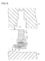
- FIGS. 1 to 6 One preferred embodiment of the present invention is described with reference to FIGS. 1 to 6.
- An insert-molded article IMA according to this embodiment is one application of the present invention to an electronic control unit (ECU) having a printed circuit board at least partly accommodated inside a casing 10.
- FIG. 1 shows the entire casing 10.
- the casing 10 is made e.g. of a synthetic resin preferably substantially into a box having an open upper or lateral surface, and the printed circuit board is at least partly accommodated and a plurality of busbars are arranged therein.
- An unillustrated cover is or is to be mounted at or on an opening of the casing 10 to ensure watertightness in the casing 10.
- one or more mount holes 11 preferably in the form of through holes used to mount the casing 10 on a body of a vehicle are formed at specified (predetermined or predeterminable) positions at or on the outer periphery of the casing 10, and the casing 10 is to be mounted on the body by bolts inserted through these mount holes 11.
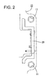
- One or more (preferably substantially strip-shaped) busbars or conductors 20 are at least partly embedded at specified (predetermined or predeterminable) parts of side walls 12 of the casing 10 along the wall surfaces of the side walls 12.
- the busbar 20 at least partly embedded in a bulging portion of the lateral (right) side wall 12 shown in FIG. 1 is crank-shaped and ends thereof at least partly project into the casing 10 to be connectable with the printed circuit board and electric or electronic components.
- an inner portion 30 having the one or more busbars 20 as inserts is used as an insert.
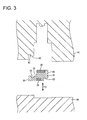
- the inner portion 30 is, as shown in FIG. 3, comprised of two busbars 20 spaced apart by a specified (predetermined or predeterminable) distance along thickness direction TD (or a direction substantially normal to the longitudinal direction of the busbars 20) and a holding portion 31 made e.g. of a synthetic resin for covering the facing surfaces of the respective busbars 20, wherein the respective busbars 20 are held at a specified (predetermined or predeterminable) spacing or distance by the holding portion 31.
- One or more recesses 32 having substantially L-shaped cross sections (or each opening to two lateral sides of the holding portion 31) are formed at a first (right lower) corner and a second (left upper) corner (substantially diagonally opposite to the first corner) of the holding portion 31 shown in FIG. 3.
- a resin portion 13 (to be described later) of the casing 10 at least partly enters these recesses 32 to enhance an engaging force with the resin portion 13, so that the inner portion 30 does not come out of the casing 10.
- An interlocking portion 33 made of a synthetic resin is so formed as to be substantially continuous with the holding portion 31 at the lateral (left) side of the busbar 20 disposed at a lower side in FIG. 3.
- the interlocking portion 33 is formed to substantially horizontally project from its base end toward its leading end, and can be hooked in a mold for secondary molding, and the inner portion 30 is so positioned and supported in the mold 61 as to project from the inner wall surface of the mold 61 by the engagement of the interlocking portion 33 and the mold 61.
- a recess 34 is formed at the base end or extending portion of the interlocking portion 33, and the inner portion 30 is prevented from lateral loose movements by the engagement of this recess 34 and a projection 63 formed in the mold 61.
- the recess 34 is so formed in the lateral (upper) surface of the interlocking portion 33 as to be open upward or laterally and have a substantially U-shaped cross section, and is closely engageable with the projection 63.
- the casing 10 is formed by insert molding using the above inner portion 30 as an insert such that the inner portion 30 excluding the interlocking portion 33 is at least partly, preferably substantially completely covered by the resin portion 13 (made of the preferably same synthetic resin as the holding portion 31).
- the interlocking portion 33 is located at the inner surface of the casing 10 and projects toward the inside of the casing 10 from the inner surface of the casing 10 with the recess 34 as a border.
- This mold is comprised of a lower mold 60 and an upper mold 61 as shown in FIG. 3.
- the upper mold 61 is provided with a receiving portion 62 recessed substantially in conformity with the shape of the interlocking portion 33, and the aforementioned projection 63 is provided on the inner wall surface of this receiving portion 62 to project downward or laterally.
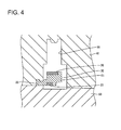
- the interlocking portion 33 is engageable with the receiving portion 62 as the mold 61, 62 is closed. As being engaged with the receiving portion 62, the interlocking portion 33 is tightly held between the upper mold 61 and the lower mold 60 and projects in a cavity 66.
- the inner portion 30 is formed by insert molding using the one or more busbars 20 as inserts. Subsequently, as shown in FIGS. 3 and 4, the lower and upper molds 60, 61 are brought to the inner portion 30, thereby closing the mold to at least partly fit the interlocking portion 33 in the receiving portion 62. As the mold closing is completed, the interlocking portion 33 is tightly held between the upper and lower molds 61, 60 and the recess 34 of the interlocking portion 33 and the projection 63 of the upper mold 61 are engaged with each other, with the result that the inner portion 30 is so positioned and supported as to project from the inner wall surface of the mold while being prevented from lateral and vertical loose movements.
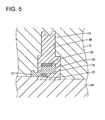
- Molten resin is injected to at least partly fill the cavity 66 of the mold in this state.
- the substantially entire casing 10 including a side wall portion shown in FIG. 6 is obtained.
- the casing 10 as a finished article is such that the interlocking portion 33 is exposed at the inner surface thereof and the holding portion 31 is preferably substantially entirely covered by the resin portion 13.
- the interlocking portion 33 is hooked in or interlocked with the mold to thereby position and support the inner portion 30 in the mold in such a manner as to project from the inner wall surface of the mold during the insert molding using the inner portion 30 as an insert.
- the preferably substantially entire inner portion 30 excluding the interlocking portion 33 can be covered by the resin portion 13.
- the interlocking portion 33 is formed to project toward the inside of the casing 10 from the inner surface of the casing 10, insert molding can be carried out with the interlocking portion 33 tightly held between the upper and lower molds 61, 60. Therefore, the construction of the mold can be simplified.
- a casing 10 is formed by insert molding using an inner portion 30 holding one or more busbars or conductors 20 as an insert.
- the inner portion 30 includes an interlocking portion 33 to be hooked in a mold for molding the casing 10, and is so positioned and supported in the mold by the presence of the interlocking portion 33 as to project from the inner wall surface of the mold.
- the interlocking portion 33 is formed to project substantially toward the inside of the casing 10 from the inner surface of the casing 10.
- the casing 10 is formed by at least partly covering the inner portion 30 substantially excluding the interlocking portion 33 by a resin portion 13.
Landscapes
- Engineering & Computer Science (AREA)
- Manufacturing & Machinery (AREA)
- Mechanical Engineering (AREA)
- Microelectronics & Electronic Packaging (AREA)
- Injection Moulding Of Plastics Or The Like (AREA)
- Moulds For Moulding Plastics Or The Like (AREA)
- Casings For Electric Apparatus (AREA)
Applications Claiming Priority (2)
| Application Number | Priority Date | Filing Date | Title |
|---|---|---|---|
| JP2004117838A JP4189753B2 (ja) | 2004-04-13 | 2004-04-13 | インサート成形品及びインサート成形品の製造方法 |
| JP2004117838 | 2004-04-13 |
Publications (2)
| Publication Number | Publication Date |
|---|---|
| EP1587183A1 true EP1587183A1 (de) | 2005-10-19 |
| EP1587183B1 EP1587183B1 (de) | 2008-08-27 |
Family
ID=34934880
Family Applications (1)
| Application Number | Title | Priority Date | Filing Date |
|---|---|---|---|
| EP05007684A Expired - Lifetime EP1587183B1 (de) | 2004-04-13 | 2005-04-07 | Gegenstand mit eingegossenem Einsatz und Herstellungsverfahren |
Country Status (5)
| Country | Link |
|---|---|
| US (1) | US7560153B2 (de) |
| EP (1) | EP1587183B1 (de) |
| JP (1) | JP4189753B2 (de) |
| CN (1) | CN100417508C (de) |
| DE (1) | DE602005009276D1 (de) |
Cited By (4)
| Publication number | Priority date | Publication date | Assignee | Title |
|---|---|---|---|---|
| WO2008043691A1 (de) * | 2006-10-10 | 2008-04-17 | Robert Bosch Gmbh | Gespritztes kunststoffbauteil mit einlegeteil |
| EP2500985A1 (de) * | 2011-03-15 | 2012-09-19 | Sumitomo Wiring Systems, Ltd. | Vorrichtungsverbinder und Herstellungsverfahren dafür |
| EP3093116A1 (de) * | 2015-05-13 | 2016-11-16 | Stefan Pfaff Werkzeug- und Formenbau GmbH & Co. KG | Herstellungs- und positionierverfahren für dichtungsprofile |
| WO2017042346A1 (de) * | 2015-09-10 | 2017-03-16 | Stefan Pfaff Werkzeug- Und Formenbau Gmbh & Co. Kg | Herstellungs- und positionierverfahren für dichtungsprofile |
Families Citing this family (20)
| Publication number | Priority date | Publication date | Assignee | Title |
|---|---|---|---|---|
| JP4679327B2 (ja) | 2005-10-12 | 2011-04-27 | 株式会社リコー | 画像形成装置 |
| JP4720648B2 (ja) * | 2006-06-29 | 2011-07-13 | 住友電装株式会社 | 樹脂成形品の製造方法 |
| JP2010105337A (ja) * | 2008-10-31 | 2010-05-13 | Nissha Printing Co Ltd | インサート2色成形方法および2色成形金型装置並びにインサート2色成形品 |
| JP5509737B2 (ja) * | 2009-03-25 | 2014-06-04 | アイシン精機株式会社 | ソレノイドバルブの取付構造 |
| KR101101491B1 (ko) * | 2010-02-25 | 2012-01-03 | 삼성전기주식회사 | 안테나 패턴 프레임, 전자장치 케이스 및 이의 제조금형 |
| KR101053336B1 (ko) * | 2010-03-15 | 2011-08-01 | 삼성전기주식회사 | 안테나 패턴 프레임, 전자장치 케이스 및 이의 제조금형 |
| JP5626047B2 (ja) * | 2011-03-15 | 2014-11-19 | 住友電装株式会社 | 機器用コネクタ |
| JP5846802B2 (ja) * | 2011-08-11 | 2016-01-20 | 矢崎総業株式会社 | コネクタおよびそのコネクタの製造方法 |
| JP5661087B2 (ja) * | 2012-11-30 | 2015-01-28 | 東海興業株式会社 | インサート成形品、インサート成形方法、及びインサート成形装置 |
| JP6155057B2 (ja) * | 2013-03-08 | 2017-06-28 | Kyb株式会社 | バスバーユニット製造方法及びバスバーユニット |
| JP6610413B2 (ja) * | 2016-04-26 | 2019-11-27 | 中西金属工業株式会社 | インサート成形品の製造方法 |
| JP6605417B2 (ja) * | 2016-08-31 | 2019-11-13 | 東海興業株式会社 | 樹脂成形品及びその製造方法 |
| FR3059202B1 (fr) * | 2016-11-18 | 2019-08-16 | Continental Automotive France | Procede de fabrication sur une plaque de maintien d'un module electronique avec des formes de positionnement depassant du surmoulage final |
| ES2766768T3 (es) * | 2017-04-10 | 2020-06-15 | Gemue Gebr Mueller Appbau Gmbh & Co Kg | Método de fabricación de una membrana elastómera |
| US10768358B2 (en) * | 2017-08-17 | 2020-09-08 | Dura Operating, Llc | Printed film with mounted light emitting diodes encapsulated in light guide |
| JP7317471B2 (ja) * | 2018-04-17 | 2023-07-31 | 本田技研工業株式会社 | 成形体及び成形型 |
| CN109016328A (zh) * | 2018-05-29 | 2018-12-18 | 广东联塑科技实业有限公司 | 一种带钢骨架pe阀体的制备方法 |
| JP7077928B2 (ja) * | 2018-12-06 | 2022-05-31 | 住友電装株式会社 | コネクタ及びその製造方法 |
| JP7007512B1 (ja) * | 2021-05-31 | 2022-02-10 | 株式会社アテックス | 導電部材及びその製造方法 |
| JP7544780B2 (ja) | 2022-10-04 | 2024-09-03 | 矢崎総業株式会社 | 樹脂成形品 |
Citations (3)
| Publication number | Priority date | Publication date | Assignee | Title |
|---|---|---|---|---|
| DE19504828A1 (de) * | 1995-02-14 | 1996-08-22 | Fritz Richard Gmbh & Co Kg | Verfahren zum Herstellen und Verbinden eines Rahmens mit einer Glasscheibe und Vorrichtung zum Durchführen des Verfahrens |
| US6294851B1 (en) * | 1998-06-10 | 2001-09-25 | Asmo Co., Ltd. | Resin molding method for inserting terminal and connector for motor having the terminal |
| US20040002260A1 (en) * | 2002-06-28 | 2004-01-01 | Sumitomo Wiring Systems, Ltd. | Insert-molded connector and method of forming it |
Family Cites Families (3)
| Publication number | Priority date | Publication date | Assignee | Title |
|---|---|---|---|---|
| CN2030764U (zh) * | 1987-07-14 | 1989-01-11 | 施吾铨 | 带保险丝插头 |
| JP3870467B2 (ja) * | 1996-03-12 | 2007-01-17 | 株式会社デンソー | 電気接続部を有する成形品とその成形方法 |
| CN2296079Y (zh) * | 1997-11-05 | 1998-10-28 | 中国航天工业总公司第二研究院二○三所 | 万能电源插座 |
-
2004
- 2004-04-13 JP JP2004117838A patent/JP4189753B2/ja not_active Expired - Lifetime
-
2005
- 2005-04-07 EP EP05007684A patent/EP1587183B1/de not_active Expired - Lifetime
- 2005-04-07 DE DE602005009276T patent/DE602005009276D1/de not_active Expired - Lifetime
- 2005-04-11 US US11/103,833 patent/US7560153B2/en active Active
- 2005-04-13 CN CNB2005100649978A patent/CN100417508C/zh not_active Expired - Lifetime
Patent Citations (3)
| Publication number | Priority date | Publication date | Assignee | Title |
|---|---|---|---|---|
| DE19504828A1 (de) * | 1995-02-14 | 1996-08-22 | Fritz Richard Gmbh & Co Kg | Verfahren zum Herstellen und Verbinden eines Rahmens mit einer Glasscheibe und Vorrichtung zum Durchführen des Verfahrens |
| US6294851B1 (en) * | 1998-06-10 | 2001-09-25 | Asmo Co., Ltd. | Resin molding method for inserting terminal and connector for motor having the terminal |
| US20040002260A1 (en) * | 2002-06-28 | 2004-01-01 | Sumitomo Wiring Systems, Ltd. | Insert-molded connector and method of forming it |
Cited By (4)
| Publication number | Priority date | Publication date | Assignee | Title |
|---|---|---|---|---|
| WO2008043691A1 (de) * | 2006-10-10 | 2008-04-17 | Robert Bosch Gmbh | Gespritztes kunststoffbauteil mit einlegeteil |
| EP2500985A1 (de) * | 2011-03-15 | 2012-09-19 | Sumitomo Wiring Systems, Ltd. | Vorrichtungsverbinder und Herstellungsverfahren dafür |
| EP3093116A1 (de) * | 2015-05-13 | 2016-11-16 | Stefan Pfaff Werkzeug- und Formenbau GmbH & Co. KG | Herstellungs- und positionierverfahren für dichtungsprofile |
| WO2017042346A1 (de) * | 2015-09-10 | 2017-03-16 | Stefan Pfaff Werkzeug- Und Formenbau Gmbh & Co. Kg | Herstellungs- und positionierverfahren für dichtungsprofile |
Also Published As
| Publication number | Publication date |
|---|---|
| EP1587183B1 (de) | 2008-08-27 |
| DE602005009276D1 (de) | 2008-10-09 |
| JP4189753B2 (ja) | 2008-12-03 |
| CN1683140A (zh) | 2005-10-19 |
| US7560153B2 (en) | 2009-07-14 |
| CN100417508C (zh) | 2008-09-10 |
| US20050227036A1 (en) | 2005-10-13 |
| JP2005297387A (ja) | 2005-10-27 |
Similar Documents
| Publication | Publication Date | Title |
|---|---|---|
| EP1587183B1 (de) | Gegenstand mit eingegossenem Einsatz und Herstellungsverfahren | |
| EP2500995B1 (de) | Herstellungsverfahren für einen Verbinder | |
| EP2500997B1 (de) | Verbinder und Verfahren zu dessen Herstellung | |
| EP2500985B1 (de) | Vorrichtungsverbinder und Herstellungsverfahren dafür | |
| EP1810810B1 (de) | Aufbau zum Giessen und Giessverfahren für ein Kunststoffteil | |
| EP0853356B1 (de) | Verfahren zum Herstellen eines Verbinders und ein Verbinder hergestellt durch Formen mit Einsetzung und dessen Verwendung | |
| JP7850379B2 (ja) | ヒューズユニット及びヒューズユニットの製造方法 | |
| JPH04263913A (ja) | 金属部材の樹脂インサート成形方法 | |
| JP6798436B2 (ja) | 回路装置、回路装置の製造方法、およびコネクタ | |
| EP2234222A1 (de) | Abgeschirmter Verbinder und Herstellungsverfahren dafür | |
| JP2005288763A (ja) | インサート成形品の製造方法 | |
| US6045739A (en) | Method of manufacturing a molded product internally having inserts in a layered state | |
| JP3287532B2 (ja) | インサート成形方法 | |
| JP7077928B2 (ja) | コネクタ及びその製造方法 | |
| US20120258619A1 (en) | Connector and electrical connection box | |
| US6203358B1 (en) | Electrical connection box and a method for manufacturing such an electrical connection box | |
| JP7099290B2 (ja) | リアクトルの製造方法 | |
| JP2006315280A (ja) | コネクタ付きケースの成形構造 | |
| JP2006281622A (ja) | 二重樹脂射出成型方法、その方法で成型された樹脂製品及びオルタネータ用レギュレータケース | |
| JP4863954B2 (ja) | 電子ユニットおよびその製造方法 | |
| CN109891681A (zh) | 连接器 | |
| JP5526806B2 (ja) | 回路構成体、回路構成体の製造方法、および電気接続箱 | |
| JP6962899B2 (ja) | 電子部品及び電子部品の製造方法 | |
| JP2005295628A (ja) | インサート成形品 | |
| KR20240058794A (ko) | 방수 전자기 디바이스 및 그 제조 방법 |
Legal Events
| Date | Code | Title | Description |
|---|---|---|---|
| PUAI | Public reference made under article 153(3) epc to a published international application that has entered the european phase |
Free format text: ORIGINAL CODE: 0009012 |
|
| 17P | Request for examination filed |
Effective date: 20050414 |
|
| AK | Designated contracting states |
Kind code of ref document: A1 Designated state(s): AT BE BG CH CY CZ DE DK EE ES FI FR GB GR HU IE IS IT LI LT LU MC NL PL PT RO SE SI SK TR |
|
| AX | Request for extension of the european patent |
Extension state: AL BA HR LV MK YU |
|
| AKX | Designation fees paid |
Designated state(s): DE |
|
| GRAP | Despatch of communication of intention to grant a patent |
Free format text: ORIGINAL CODE: EPIDOSNIGR1 |
|
| RIN1 | Information on inventor provided before grant (corrected) |
Inventor name: TAKANASHI, HITOSHI |
|
| GRAS | Grant fee paid |
Free format text: ORIGINAL CODE: EPIDOSNIGR3 |
|
| GRAA | (expected) grant |
Free format text: ORIGINAL CODE: 0009210 |
|
| AK | Designated contracting states |
Kind code of ref document: B1 Designated state(s): DE |
|
| REF | Corresponds to: |
Ref document number: 602005009276 Country of ref document: DE Date of ref document: 20081009 Kind code of ref document: P |
|
| REG | Reference to a national code |
Ref country code: DE Ref legal event code: R096 Ref document number: 602005009276 Country of ref document: DE Effective date: 20081009 |
|
| PLBE | No opposition filed within time limit |
Free format text: ORIGINAL CODE: 0009261 |
|
| STAA | Information on the status of an ep patent application or granted ep patent |
Free format text: STATUS: NO OPPOSITION FILED WITHIN TIME LIMIT |
|
| 26N | No opposition filed |
Effective date: 20090528 |
|
| REG | Reference to a national code |
Ref country code: DE Ref legal event code: R097 Ref document number: 602005009276 Country of ref document: DE Effective date: 20090528 |
|
| REG | Reference to a national code |
Ref country code: DE Ref legal event code: R084 Ref document number: 602005009276 Country of ref document: DE |
|
| P01 | Opt-out of the competence of the unified patent court (upc) registered |
Effective date: 20230517 |
|
| PGFP | Annual fee paid to national office [announced via postgrant information from national office to epo] |
Ref country code: DE Payment date: 20240227 Year of fee payment: 20 |
|
| REG | Reference to a national code |
Ref country code: DE Ref legal event code: R071 Ref document number: 602005009276 Country of ref document: DE |