EP1582884A1 - Halbleiter-Motorantriebsschaltung mit Erkennung des Endes der Lebensdauer - Google Patents
Halbleiter-Motorantriebsschaltung mit Erkennung des Endes der Lebensdauer Download PDFInfo
- Publication number
- EP1582884A1 EP1582884A1 EP05006808A EP05006808A EP1582884A1 EP 1582884 A1 EP1582884 A1 EP 1582884A1 EP 05006808 A EP05006808 A EP 05006808A EP 05006808 A EP05006808 A EP 05006808A EP 1582884 A1 EP1582884 A1 EP 1582884A1
- Authority
- EP
- European Patent Office
- Prior art keywords
- wire
- dummy
- main circuit
- power semiconductor
- electrode
- Prior art date
- Legal status (The legal status is an assumption and is not a legal conclusion. Google has not performed a legal analysis and makes no representation as to the accuracy of the status listed.)
- Granted
Links
Images


Classifications
-
- G—PHYSICS
- G01—MEASURING; TESTING
- G01R—MEASURING ELECTRIC VARIABLES; MEASURING MAGNETIC VARIABLES
- G01R31/00—Arrangements for testing electric properties; Arrangements for locating electric faults; Arrangements for electrical testing characterised by what is being tested not provided for elsewhere
- G01R31/28—Testing of electronic circuits, e.g. by signal tracer
- G01R31/2851—Testing of integrated circuits [IC]
- G01R31/2884—Testing of integrated circuits [IC] using dedicated test connectors, test elements or test circuits on the IC under test
-
- H—ELECTRICITY
- H10—SEMICONDUCTOR DEVICES; ELECTRIC SOLID-STATE DEVICES NOT OTHERWISE PROVIDED FOR
- H10W—GENERIC PACKAGES, INTERCONNECTIONS, CONNECTORS OR OTHER CONSTRUCTIONAL DETAILS OF DEVICES COVERED BY CLASS H10
- H10W72/00—Interconnections or connectors in packages
- H10W72/071—Connecting or disconnecting
- H10W72/075—Connecting or disconnecting of bond wires
- H10W72/07531—Techniques
- H10W72/07532—Compression bonding, e.g. thermocompression bonding
- H10W72/07533—Ultrasonic bonding, e.g. thermosonic bonding
-
- H—ELECTRICITY
- H10—SEMICONDUCTOR DEVICES; ELECTRIC SOLID-STATE DEVICES NOT OTHERWISE PROVIDED FOR
- H10W—GENERIC PACKAGES, INTERCONNECTIONS, CONNECTORS OR OTHER CONSTRUCTIONAL DETAILS OF DEVICES COVERED BY CLASS H10
- H10W72/00—Interconnections or connectors in packages
- H10W72/071—Connecting or disconnecting
- H10W72/075—Connecting or disconnecting of bond wires
- H10W72/07551—Connecting or disconnecting of bond wires characterised by changes in properties of the bond wires during the connecting
- H10W72/07552—Connecting or disconnecting of bond wires characterised by changes in properties of the bond wires during the connecting changes in structures or sizes
-
- H—ELECTRICITY
- H10—SEMICONDUCTOR DEVICES; ELECTRIC SOLID-STATE DEVICES NOT OTHERWISE PROVIDED FOR
- H10W—GENERIC PACKAGES, INTERCONNECTIONS, CONNECTORS OR OTHER CONSTRUCTIONAL DETAILS OF DEVICES COVERED BY CLASS H10
- H10W72/00—Interconnections or connectors in packages
- H10W72/071—Connecting or disconnecting
- H10W72/075—Connecting or disconnecting of bond wires
- H10W72/07551—Connecting or disconnecting of bond wires characterised by changes in properties of the bond wires during the connecting
- H10W72/07553—Connecting or disconnecting of bond wires characterised by changes in properties of the bond wires during the connecting changes in shapes
-
- H—ELECTRICITY
- H10—SEMICONDUCTOR DEVICES; ELECTRIC SOLID-STATE DEVICES NOT OTHERWISE PROVIDED FOR
- H10W—GENERIC PACKAGES, INTERCONNECTIONS, CONNECTORS OR OTHER CONSTRUCTIONAL DETAILS OF DEVICES COVERED BY CLASS H10
- H10W72/00—Interconnections or connectors in packages
- H10W72/50—Bond wires
- H10W72/521—Structures or relative sizes of bond wires
- H10W72/527—Multiple bond wires having different sizes
-
- H—ELECTRICITY
- H10—SEMICONDUCTOR DEVICES; ELECTRIC SOLID-STATE DEVICES NOT OTHERWISE PROVIDED FOR
- H10W—GENERIC PACKAGES, INTERCONNECTIONS, CONNECTORS OR OTHER CONSTRUCTIONAL DETAILS OF DEVICES COVERED BY CLASS H10
- H10W72/00—Interconnections or connectors in packages
- H10W72/50—Bond wires
- H10W72/531—Shapes of wire connectors
- H10W72/5363—Shapes of wire connectors the connected ends being wedge-shaped
-
- H—ELECTRICITY
- H10—SEMICONDUCTOR DEVICES; ELECTRIC SOLID-STATE DEVICES NOT OTHERWISE PROVIDED FOR
- H10W—GENERIC PACKAGES, INTERCONNECTIONS, CONNECTORS OR OTHER CONSTRUCTIONAL DETAILS OF DEVICES COVERED BY CLASS H10
- H10W72/00—Interconnections or connectors in packages
- H10W72/50—Bond wires
- H10W72/531—Shapes of wire connectors
- H10W72/537—Multiple bond wires having different shapes
-
- H—ELECTRICITY
- H10—SEMICONDUCTOR DEVICES; ELECTRIC SOLID-STATE DEVICES NOT OTHERWISE PROVIDED FOR
- H10W—GENERIC PACKAGES, INTERCONNECTIONS, CONNECTORS OR OTHER CONSTRUCTIONAL DETAILS OF DEVICES COVERED BY CLASS H10
- H10W72/00—Interconnections or connectors in packages
- H10W72/50—Bond wires
- H10W72/551—Materials of bond wires
- H10W72/552—Materials of bond wires comprising metals or metalloids, e.g. silver
- H10W72/5522—Materials of bond wires comprising metals or metalloids, e.g. silver comprising gold [Au]
Definitions
- the present invention relates to a motor driving system, for driving a motor, using a power semiconductor module formed, by wiring, on a power semiconductor chip.
- a drive circuit to drive a power device such as a motor, employs a power semiconductor module having a power semiconductor chip to control the drive current.
- the power semiconductor module having the power semiconductor chip controls the drive current by being energized intermittently. After the long intermittent energizing operation, the difference in the coefficient of linear expansion between the electrode and the wire, etc. and the repeated sharp temperature change during the drive operation combine to generate a thermal stress in the wire connection boundary.
- the larger wire diameter, the larger wire rigidity so that a conspicuous thermal stress in the wire connection boundary is generated.
- the wire is liable to be separated or otherwise damaged at the connection boundary, thereby posing the problem of a reduced endurance to power cycles and heat cycles (See Japanese Unexamined Patent Publication No. 2003-303845, for example).
- the separation of the wire from the electrode depends on the amount and frequency of temperature change of the semiconductor chip on the one hand and the intermittently energizing condition and the operating environment on the other hand. Therefore, the separation of the wire is affected considerably by the actual operation of the user and the time of separation is difficult to predict.
- the service life is calculated on the assumption that the power semiconductor chip is used under a maximum load in a predetermined cycle of operation.
- the service life of the power semiconductor module is calculated based on a maximum load imposed on the power semiconductor chip as described above, it may happen that the power semiconductor chip is replaced in spite of the fact that the actual load is lighter than the assumed load or power cycle and the power semiconductor chip is still usable. In the case where the load actually imposed is heavier than the assumed load or power cycle, on the contrary, the power semiconductor chip may be damaged before being replaced at the time of expiry of the calculated service life.
- the service life in terms of power cycles of the power semiconductor chip is accurately determined and the power semiconductor module is effectively used to the end of the semiconductor life while being replaced before any fault which may occur, thereby assuring satisfactory preventive maintenance.
- a motor driving system including a power semiconductor module having a built-in means for predicting the separation of the main circuit wire, whereby the approach of the separation time of the main circuit wire can be predicted.
- the time to replace the power semiconductor module used in the power devices such as the motor driving system is clarified thereby to prevent the operation failure of the motor driving system.
- the motor driving system comprises a module carrying a power semiconductor chip, wherein the power semiconductor chip includes a main circuit wire and a dummy wire connected to the electrode of the power semiconductor, and wherein the power semiconductor chip performs the rectifying operation and/or the switching operation to drive the motor.
- the main circuit wire is connected to the electrode of the power semiconductor chip to supply power between the power semiconductor chip and external devices.
- the dummy wire on the other hand, is arranged to predict the separation of the main circuit wire and has no effect on the energizing of the main circuit wire. Even in the case where the dummy wire is separated from the electrode, therefore, the energizing of the main circuit wire is not adversely affected.
- the dummy wire is connected to the same electrode to which the main circuit wire is connected, or in the case where the environment of a different electrode is considered subjected to a similar temperature change as the main circuit wire, the dummy wire may alternatively be connected to the particular different electrode.
- the connecting portions of the main circuit wire and the dummy wire with the electrode exposed to a similar operating environment such as the temperature change are considered to degenerate in a similar manner.
- the separation of the main circuit wire can be predicted based on the separation of the dummy wire.
- connection strength with the electrode is set lower for the dummy wire than for the main circuit wire.
- the wires are separated in the ascending order of connection strength.
- the dummy wire set at a low connection strength therefore, is separated before the main circuit wire thereby to positively predict the separation of the main circuit wire before the actual separation thereof.
- a plurality of dummy wires of the same or different connection strengths may be connected.
- the separation of the main circuit wire can be positively predicted based on separation of any one of the dummy wires even if the variations in actual connection strength or separation phenomenon may change the time of separation of the dummy wires.
- the degeneration degree can be determined by detecting the separation of the dummy wires sequentially.
- the wires and the electrode can be connected to each other by wire bonding or soldering.
- the main circuit wire and the dummy wire are connected under different wire bonding conditions to the electrode, resulting in different connection strength between the dummy wire and the main circuit wire.
- the bonding conditions include the pressure force and/or the ultrasonic power applied to the main circuit wire and the dummy wire.
- the dummy wire is set to a lower connection strength than the main circuit wire.
- the main circuit wire and the dummy wire are connected to the electrode by wire bonding.
- the different diameters result in different connection strength.
- the dummy wire is set to a lower connection strength.
- the wires and the electrode are connected by soldering.
- the main circuit wire and the dummy wire are connected to the electrode by soldering under different soldering conditions. In this way, the dummy wire and the main circuit wire are differentiated from each other in connection strength.
- the soldering conditions may include the soldering area and the soldering length.
- the motor driving system comprises a detection means to detect the connection condition between the dummy wire and the electrode.
- the detection means outputs a detection signal through a photo coupler. This detection signal indicates that the dummy wire arranged in the power semiconductor module has been separated from the electrode, and therefore the separation of the main circuit wire from the electrode can be predicted. This prediction, in turn, makes it possible to determine and manage the time of replacing the power semiconductor module.
- the motor driving system issues a message based on the detection signal and thus can indicate that the service life of the power indicate semiconductor module is about to expire and the time to replace the power semiconductor module.
- the motor driving system can predict the separation of the main circuit wire by detecting the separation of the dummy wire. It is therefore possible to prevent the motor drive operation failure by replacing the power semiconductor module beforehand.
- the separation of the main circuit wire can be predicted. Also, the operation failure of the power semiconductor module and the motor driving system using the power semiconductor module which otherwise might be caused by the separation of the main circuit wire can be prevented.
- Fig. 1 is a diagram for explaining the outline of a power semiconductor module of a motor driving system according to the invention.
- a power semiconductor chip 2 includes an electrode 3 for connecting the wires.
- the electrode 3 is connected with a main circuit wire 4 to supply power between the power semiconductor chip 2 and external devices and a dummy wire 5 to predict the separation of the main circuit wire 4.
- the circuit is so configured that the dummy wire 5 has no effect on the energizing of the main circuit wire 4 and, even in the case where the dummy wire 5 is separated from the electrode 3, the energizing of the main circuit wire 4 is not adversely affected.
- connection strength of the connecting portion between the dummy wire 5 and the electrode 3 is set lower than that of the connecting portion between the main circuit wire 4 and the electrode 3.
- thermal stress is generated in the connecting portion by the temperature change due to the power cycles in which the power semiconductor chip 2 is energized intermittently thereby to reduce the connection strength of the connecting portion.
- the reduction in connection strength depends on the amount and frequency of temperature change of the power semiconductor chip.
- the separation of the dummy wire 5 of the power semiconductor module 1 from the electrode 3 is detected, so that the separation of the main circuit wire 4 is predicted before actual separation thereof from the electrode 3 and the service life of the power semiconductor module is forecast.
- Figs. 2a, 2b are diagrams for explaining the connection of the main circuit wire and the dummy wire.
- Fig. 2a shows the state in which the main circuit wire 4 and the dummy wire 5 are connected to the electrode 3.
- the main circuit wire 4 is connected by bonding the connecting portion 4a thereof to the electrode 3.
- the dummy wire 5 is connected by bonding the connecting portion 5a thereof to the electrode 3.
- the connection strength of the connecting portion 5a of the dummy wire 5 is lower than that of the connecting portion 4a of the main circuit wire 4. In the case where the temperature change is repeated due to power cycles in which the power semiconductor chip 2 is energized intermittently, therefore, the dummy wire 5 is separated from the electrode 3 earlier than the main circuit wire 4 (Fig. 2b).
- Figs. 3a to 3c show an example having a plurality of dummy wires.
- the dummy wires have different connection strength, so that the service life of the connecting portion of the main circuit wire can be predicted in steps.
- Fig. 3a shows an example of configuration in which the main circuit wire 4 and two dummy wires 5A, 5B are connected to the electrode 3 through the connecting portions 4a, 5a, 5b, respectively.
- connection strength of the connecting portions 4a, 5b, 5a are set lower in that order.
- the main circuit wire 4 has the highest connection strength, while the dummy wires 5B, 5A are decreased in connection strength in that order.
- the connecting portion 5a of the dummy 5A lowest in connection strength is first separated from the electrode 3 (Fig. 3b), and the subsequent temperature change separates the dummy wire 5B of the next lowest connection strength from the electrode 3 (Fig. 3c).
- the main circuit wire 4 also comes to be separated from the electrode 3.
- the service life of the connecting portion of the main circuit wire 4 can be predicted in steps by detecting the separation of the dummy wires 5A, 5B.
- a plurality of dummy wires may have the same connection strength.
- connection strength There are variations in the actual connection strength and the phenomenon of separation and a dummy wire is not necessarily separated at a predicted time of degeneration. In spite of a variation in dummy wire separation, therefore, the separation of the main circuit wire can be positively predicted by detecting the separation of any of the dummy wires.
- Wire bonding includes the ball bonding (thermosonic bonding using heat and ultrasonic wave) using a ball prepared by fusing the forward end of the wire, and wedge bonding (ultrasonic bonding) for connecting the wire directly using a bonding tool.
- the forward end of the wire supplied through a guide in a capillary is fused by sparks into the shape of ball and the ball is bonded on the pad on the semiconductor chip side. Then, the bonding is completed by ultrasonic energy and heating from a stage.
- a wedge tool is mounted at the forward end of a horn adapted to be vibrated by an ultrasonic vibrator, and the wire supplied from a wire feeder is held at the bonding point by the forward end of the wedge tool. Under this condition, pressure force and ultrasonic vibration are applied to the wire through the wedge tool. Heat is generated on the bonding surface based on the friction between the wire and the bonding point, so that the wire is plastically deformed and connected to the bonding point.
- connection strength of the dummy wire can be adjusted in various ways in accordance with the connecting method in which the wire is connected to the electrode.
- connection strength of the dummy wire can be adjusted according to the bonding conditions.
- the bonding conditions include the heating temperature of the electrode and the wire, the time during which the ultrasonic wave is applied, the ultrasonic wave power with which the wire is plastically deformed and the load, from the capillary, to hold the wire.
- the diffusion bonding of gold between a gold wire and the electrode, for example, becomes active and improves the bonding.
- the bonding characteristic is said to be degenerated by the softening of the substrate.
- the bonding is the phenomenon of diffusion due to heat and ultrasonic energy combined, and therefore a sufficient bonding cannot be secured if the application time of ultrasonic wave is short.
- the applied ultrasonic power contributes, as ultrasonic energy, to the plastic deformation of the wire by combining with the application time of ultrasonic waves. An excessively large power, however, would deform the wire to an unnecessary degree and reduce the strength.
- the bonding conditions for ultrasonic bonding include the ultrasonic wave application time, the ultrasonic wave application output and the load (See Japanese Unexamined Patent Publication No. 5-74876).
- connection strength of the dummy wire can be set in accordance with the pressure force or ultrasonic power included in the bonding conditions, and the pressure force or the ultrasonic power, in turn, can be adjusted by the current and/or the application time of the bonding device.
- connection strength can be changed also by differentiating the diameter of the main circuit wire and that of the dummy wire from each other.
- Figs. 4a, 4b are diagrams showing an example of dummy wires having different diameters.
- Figs. 4a, 4b show an example of configuration in which the main circuit wire 4 and the dummy wire 5 are connected to the electrode 3 through connecting portions 4a, 5a, respectively.
- the connection strength can be differentiated from each other. In the case where wires of different diameters are connected under the same bonding conditions, the resultant difference in plastic deformation of the wires leads to a different connection strength with the electrode.
- the dummy wire 5 can be set to a lower connection strength than the main circuit wire 4.
- Fig. 4a for example, if the dummy wire 5 whose diameter is larger than that the main circuit wire 4 is connected to the electrode 3 under the same bonding conditions as the main circuit wire 4, the dummy wire 5 is lower in connection strength than the main circuit wire 4, and therefore separated earlier than the main circuit wire 4 (Fig. 4b).
- connection strengths may be adjusted by differentiating the lengths 4L, 5L of the connecting portions 4a, 5a. Namely, if the length 5L of the connecting portion 5a in Fig. 2a is shorter than the length 4L of the connecting portions 4a, the dummy wire 5 is lower in connection strength than the main circuit wire 4 and, therefore, separates earlier than the main circuit wire 4.
- the main circuit wire 4 and the dummy wire 5 can also be connected to the electrode 3 by soldering and, similarly, the connection strength can be differentiated by differentiating the soldering conditions.
- the soldering conditions include the soldering area and the soldering length (See the length 4L, 5L of the connecting portions 4a, 5a in Fig. 2a).
- the main circuit wire 4 and the dummy wire 5 may be connected to either the same electrode 3 or different electrodes.
- the dummy wire 5 is preferably connected to an electrode in an environment subjected to a temperature change similar to the main circuit wire 4.
- Fig. 5 is a diagram for explaining an example of a configuration of the detection circuit.
- the electrode 3 of the power semiconductor chip 2 is connected to the main circuit wire 4 and the dummy wire 5.
- the detection circuit 6 for detecting the connection condition of the dummy wire 5 can be configured of a resistor 6a and a photocoupler 6b.
- the one end of the resistor 6a is connected to a power supply Vcc, and the other end thereof is connected to an end of the dummy wire 5.
- Vcc power supply
- the photocoupler 6b outputs a life detection signal by detecting the voltage across the resistor 6a.
- the motor driving system can generate a message based on the life detection signal output from the detection circuit 6.
- the message announced may be the form of voice, characters, image or lamp indicating that the life of the power semiconductor module 1 is about to expire or that the power semiconductor module 1 is required to be replaced.
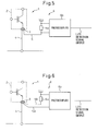
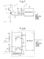
- Figs. 6 to 8 are diagrams for explaining another example of a configuration of the detection circuit including a plurality of dummy wires.
- the main circuit wire 4 and two dummy wires 5A, 5B are connected to the electrode 3 of the power semiconductor chip 2.
- the detection circuit 6 for detecting the connection condition of the dummy wires 5A, 5B can be configured of a resistor 6a and a photocoupler 6b.
- the one end of the resistor 6a is connected to a power supply Vcc and the other end thereof is connected with an end of the dummy wire 5B.
- the one end of the dummy wire 5A is connected to the photocoupler 6b.
- the photocoupler 6b cannot detect the voltage. In the case where the dummy wire 5B is separated from the electrode 3, no voltage is generated across the resistor 6a. The photocoupler 6b detects the voltage or energization across the resistor 6a and outputs a life detection signal.
- the electrode 3 of the power semiconductor chip 2 is connected with the main circuit wire 4 and two dummy wires 5A, 5B.
- the detection circuit 6 for detecting the connection condition of the dummy wires 5A, 5B can be configured of resistors 6A, 6B and a photocoupler 6b.
- the one end of the resistor 6A is connected to a power supply Vcc and the other end thereof is connected with an end of the dummy wire 5A.
- the one end of the resistor 6B is connected to a power supply Vcc and the other end thereof is connected with an end of the dummy wire 5B.
- a predetermined voltage is generated across the resistors 6A, 6B.
- no voltage is generated across the resistor 6A.
- the dummy wire 5B is separated from the electrode 3, on the other hand, no voltage is generated across the resistor 6B.
- the photocoupler 6b outputs a life detection signal upon detection of the voltages across the resistors 6A, 6B.
- Fig. 8 is a circuit diagram for explaining the detection circuit 6 of Fig. 7 in detail.
- the photocoupler 6b includes two photocoupler units driven by the voltages across the resistors 6A, 6B, respectively, and outputs a life detection signal from output terminals OUT1, OUT2, respectively, through an OR circuit.
- the life detection signal detected by the detection circuit 6 is output to the motor driving system and can predict the separation of the main circuit wire 4 of the power semiconductor module 1 or indicate an alarm. This alarm indication makes it possible to replace or repair the power semiconductor module 1 before an operation failure which may occur due to the separation of the main circuit wire 4 of the power semiconductor module 1.
- the technique according to the invention is applicable to the power devices supplied with power using the power semiconductor module 1 as well as to the motor driving system.
Landscapes
- Engineering & Computer Science (AREA)
- Computer Hardware Design (AREA)
- Microelectronics & Electronic Packaging (AREA)
- General Engineering & Computer Science (AREA)
- Physics & Mathematics (AREA)
- General Physics & Mathematics (AREA)
- Inverter Devices (AREA)
- Wire Bonding (AREA)
- Testing Of Short-Circuits, Discontinuities, Leakage, Or Incorrect Line Connections (AREA)
- Electric Connection Of Electric Components To Printed Circuits (AREA)
Applications Claiming Priority (2)
| Application Number | Priority Date | Filing Date | Title |
|---|---|---|---|
| JP2004096175 | 2004-03-29 | ||
| JP2004096175A JP4091562B2 (ja) | 2004-03-29 | 2004-03-29 | モータ駆動装置 |
Publications (2)
| Publication Number | Publication Date |
|---|---|
| EP1582884A1 true EP1582884A1 (de) | 2005-10-05 |
| EP1582884B1 EP1582884B1 (de) | 2006-08-02 |
Family
ID=34879920
Family Applications (1)
| Application Number | Title | Priority Date | Filing Date |
|---|---|---|---|
| EP20050006808 Ceased EP1582884B1 (de) | 2004-03-29 | 2005-03-29 | Halbleiter-Motorantriebsschaltung mit Erkennung des Endes der Lebensdauer |
Country Status (5)
| Country | Link |
|---|---|
| US (1) | US7098683B2 (de) |
| EP (1) | EP1582884B1 (de) |
| JP (1) | JP4091562B2 (de) |
| CN (1) | CN100364072C (de) |
| DE (1) | DE602005000057T2 (de) |
Families Citing this family (17)
| Publication number | Priority date | Publication date | Assignee | Title |
|---|---|---|---|---|
| DE102005045100A1 (de) * | 2005-09-21 | 2007-03-29 | Infineon Technologies Ag | Verfahren zum Herstellen eines Leistungshalbleitermoduls |
| JP4920319B2 (ja) * | 2006-06-22 | 2012-04-18 | 三菱電機株式会社 | 半導体素子の寿命予測回路 |
| JP2008107863A (ja) * | 2006-10-23 | 2008-05-08 | Toshiba Tec Corp | 携帯端末 |
| JP4978445B2 (ja) * | 2007-12-05 | 2012-07-18 | 株式会社デンソー | リードフレームおよび半導体装置の製造方法 |
| JP4703702B2 (ja) * | 2008-09-17 | 2011-06-15 | 株式会社東芝 | 損傷指標予測システムおよび損傷指標予測方法 |
| JP5025676B2 (ja) * | 2009-03-25 | 2012-09-12 | 株式会社東芝 | 監視装置および監視方法 |
| JP5395640B2 (ja) * | 2009-11-27 | 2014-01-22 | パナソニック株式会社 | 基板及び携帯端末装置 |
| JP2011252842A (ja) * | 2010-06-03 | 2011-12-15 | Hitachi Ltd | 素子寿命予測方法及び素子寿命予測機能を備えた回路基板 |
| CN103107111B (zh) * | 2011-11-11 | 2017-03-01 | 飞思卡尔半导体公司 | 用于监测线接合中无空气球(fab)形成的方法和装置 |
| JP5568586B2 (ja) * | 2012-03-27 | 2014-08-06 | 株式会社東芝 | 電子装置、故障判定方法、寿命推定方法 |
| JP6037464B2 (ja) | 2014-05-29 | 2016-12-07 | インターナショナル・ビジネス・マシーンズ・コーポレーションInternational Business Machines Corporation | 電気機器の寿命を予測する装置及び方法 |
| JP6550761B2 (ja) * | 2015-01-27 | 2019-07-31 | 日本電気株式会社 | 半導体集積回路の寿命予測装置 |
| EP3226014B1 (de) * | 2016-03-30 | 2024-01-10 | Mitsubishi Electric R&D Centre Europe B.V. | Verfahren zur schätzung eines beschädigungsniveaus oder einer lebensdauererwartung eines leistungshalbleitermoduls mit mindestens einem chip |
| CN110800104A (zh) | 2017-06-22 | 2020-02-14 | 三菱电机株式会社 | 半导体模块 |
| JP7318493B2 (ja) * | 2019-11-12 | 2023-08-01 | 株式会社デンソー | 半導体装置 |
| JP7052826B2 (ja) * | 2020-06-16 | 2022-04-12 | 富士電機株式会社 | 半導体装置 |
| JP2024165288A (ja) | 2023-05-17 | 2024-11-28 | 三菱電機株式会社 | 半導体装置およびインバータ装置 |
Citations (4)
| Publication number | Priority date | Publication date | Assignee | Title |
|---|---|---|---|---|
| US5673028A (en) * | 1993-01-07 | 1997-09-30 | Levy; Henry A. | Electronic component failure indicator |
| US20010002723A1 (en) * | 1999-12-07 | 2001-06-07 | Rohm Co., Ltd. | Motor driving device |
| US20020093360A1 (en) * | 2001-01-16 | 2002-07-18 | Junichi Nagata | Integrate circuit device |
| EP1398639A2 (de) * | 2002-09-13 | 2004-03-17 | Chartered Semiconductor Manufacturing Pte Ltd. | Teststruktur für Chip-integrierte Prüfung in Realzeit |
Family Cites Families (14)
| Publication number | Priority date | Publication date | Assignee | Title |
|---|---|---|---|---|
| US5176310A (en) * | 1988-11-28 | 1993-01-05 | Hitachi, Ltd. | Method and apparatus for wire bond |
| JP2705331B2 (ja) * | 1991-02-27 | 1998-01-28 | 三菱電機株式会社 | ヒューズ断検出回路 |
| JPH0574876A (ja) | 1991-09-12 | 1993-03-26 | Ricoh Co Ltd | ワイヤボンデイング装置 |
| DE19700963C2 (de) * | 1997-01-14 | 2000-12-21 | Telefunken Microelectron | Verfahren zur Herstellung eines Leistungsmoduls mit einer aktive Halbleiterbauelemente und passive Halbleiterbauelemente aufweisenden Schaltungsanordnung |
| KR20010023983A (ko) * | 1997-10-20 | 2001-03-26 | 가나이 쓰토무 | 반도체 모듈 및 이를 이용한 전력 변환 장치 |
| KR100265461B1 (ko) * | 1997-11-21 | 2000-09-15 | 윤종용 | 더미본딩와이어를포함하는반도체집적회로소자 |
| US6452502B1 (en) * | 1998-10-15 | 2002-09-17 | Intel Corporation | Method and apparatus for early detection of reliability degradation of electronic devices |
| JP2000183117A (ja) | 1998-12-10 | 2000-06-30 | Matsushita Electric Works Ltd | ワイヤボンディング評価方法と装置及びその記録媒体 |
| JP2001015541A (ja) * | 1999-06-28 | 2001-01-19 | Sumitomo Electric Ind Ltd | 半導体装置および半導体装置の製造方法 |
| US6140926A (en) * | 1999-07-21 | 2000-10-31 | Hewlett-Packard Company | Redundant status indicators for fault tolerance |
| US6987383B2 (en) * | 2000-02-10 | 2006-01-17 | Matsushita Electric Industrial Co., Ltd. | Semiconductor device having a connection inspecting circuit for inspecting connections of power source terminals and grounding terminals, and inspection method for the same |
| GB0018643D0 (en) * | 2000-07-31 | 2000-09-13 | Koninkl Philips Electronics Nv | Semiconductor devices |
| JP3506377B2 (ja) * | 2001-04-09 | 2004-03-15 | 松下電器産業株式会社 | 半導体装置およびその製造方法 |
| JP2003303845A (ja) | 2002-04-10 | 2003-10-24 | Fuji Electric Co Ltd | 半導体装置およびワイヤボンディング方法 |
-
2004
- 2004-03-29 JP JP2004096175A patent/JP4091562B2/ja not_active Expired - Fee Related
-
2005
- 2005-03-28 CN CNB2005100588103A patent/CN100364072C/zh not_active Expired - Fee Related
- 2005-03-29 US US11/092,552 patent/US7098683B2/en not_active Expired - Fee Related
- 2005-03-29 EP EP20050006808 patent/EP1582884B1/de not_active Ceased
- 2005-03-29 DE DE200560000057 patent/DE602005000057T2/de not_active Expired - Fee Related
Patent Citations (4)
| Publication number | Priority date | Publication date | Assignee | Title |
|---|---|---|---|---|
| US5673028A (en) * | 1993-01-07 | 1997-09-30 | Levy; Henry A. | Electronic component failure indicator |
| US20010002723A1 (en) * | 1999-12-07 | 2001-06-07 | Rohm Co., Ltd. | Motor driving device |
| US20020093360A1 (en) * | 2001-01-16 | 2002-07-18 | Junichi Nagata | Integrate circuit device |
| EP1398639A2 (de) * | 2002-09-13 | 2004-03-17 | Chartered Semiconductor Manufacturing Pte Ltd. | Teststruktur für Chip-integrierte Prüfung in Realzeit |
Also Published As
| Publication number | Publication date |
|---|---|
| CN1677633A (zh) | 2005-10-05 |
| EP1582884B1 (de) | 2006-08-02 |
| US7098683B2 (en) | 2006-08-29 |
| CN100364072C (zh) | 2008-01-23 |
| JP2005286009A (ja) | 2005-10-13 |
| JP4091562B2 (ja) | 2008-05-28 |
| DE602005000057D1 (de) | 2006-09-14 |
| US20050212549A1 (en) | 2005-09-29 |
| DE602005000057T2 (de) | 2007-01-04 |
Similar Documents
| Publication | Publication Date | Title |
|---|---|---|
| US7098683B2 (en) | Motor driving system having power semiconductor module life detection function | |
| EP0540189B1 (de) | Steuerungssystem | |
| KR101511893B1 (ko) | 와이어 본딩 장치 및 와이어 본딩 방법 | |
| US12206134B2 (en) | Method for electrically contacting a battery block | |
| US20100181367A1 (en) | Wire bonding apparatus and wire bonding method | |
| KR101897081B1 (ko) | 방전 검사 장치, 와이어 본딩 장치 및 방전 검사 방법 | |
| WO2011152151A1 (ja) | 素子寿命予測方法及び素子寿命予測機能を備えた回路基板 | |
| JP5104016B2 (ja) | パワー半導体モジュール | |
| US7591409B2 (en) | Semiconductor device bonding apparatus and method for bonding semiconductor device using the same | |
| JP2007335708A (ja) | ワイヤボンダ、ワイヤボンディング方法及びプログラム | |
| US7213741B2 (en) | Lead wire bonding method | |
| GB2270868A (en) | Wire bonding control system. | |
| US7420382B2 (en) | Apparatus and method for testing semiconductor chip | |
| JP4210269B2 (ja) | 超音波フリップチップ実装装置 | |
| US20260098793A1 (en) | Wire bond pull test apparatus, test equipment, test method | |
| JPH08335616A (ja) | 半導体装置及びその検査方法 | |
| JP2904194B2 (ja) | ワイヤーボンディング装置 | |
| KR20210033909A (ko) | 와이어 본딩 장치 및 와이어 본딩 방법 | |
| JP2006303168A (ja) | ワイヤボンディング方法及び装置 | |
| CN121587083A (zh) | 电加热装置和用于制造电加热装置的方法 | |
| JP2024139019A (ja) | 超音波接合方法、超音波接合装置および超音波接合システム | |
| JPH0758178A (ja) | 半導体受発光素子の選別方法およびその装置 | |
| JP2005268676A (ja) | 電子部品の接合装置および電子部品の接合方法 | |
| JPH06326161A (ja) | 超音波式ワイボンダーにおける良否判別装置 | |
| JPH0368148A (ja) | ワイヤボンダーにおけるボール形成方法 |
Legal Events
| Date | Code | Title | Description |
|---|---|---|---|
| PUAI | Public reference made under article 153(3) epc to a published international application that has entered the european phase |
Free format text: ORIGINAL CODE: 0009012 |
|
| AK | Designated contracting states |
Kind code of ref document: A1 Designated state(s): AT BE BG CH CY CZ DE DK EE ES FI FR GB GR HU IE IS IT LI LT LU MC NL PL PT RO SE SI SK TR |
|
| AX | Request for extension of the european patent |
Extension state: AL BA HR LV MK YU |
|
| 17P | Request for examination filed |
Effective date: 20050927 |
|
| GRAP | Despatch of communication of intention to grant a patent |
Free format text: ORIGINAL CODE: EPIDOSNIGR1 |
|
| RIN1 | Information on inventor provided before grant (corrected) |
Inventor name: HORIKOSHI, SHINICHI, C/O ROOM 14-206 Inventor name: MATSUBARA, SHUNSUKE Inventor name: MAKITA, HAJIME, C/O ROOM 11-501 |
|
| AKX | Designation fees paid |
Designated state(s): DE |
|
| GRAS | Grant fee paid |
Free format text: ORIGINAL CODE: EPIDOSNIGR3 |
|
| GRAA | (expected) grant |
Free format text: ORIGINAL CODE: 0009210 |
|
| AK | Designated contracting states |
Kind code of ref document: B1 Designated state(s): DE |
|
| REF | Corresponds to: |
Ref document number: 602005000057 Country of ref document: DE Date of ref document: 20060914 Kind code of ref document: P |
|
| PLBI | Opposition filed |
Free format text: ORIGINAL CODE: 0009260 |
|
| 26 | Opposition filed |
Opponent name: INFINEON TECHNOLOGIES AG Effective date: 20070502 |
|
| PLAX | Notice of opposition and request to file observation + time limit sent |
Free format text: ORIGINAL CODE: EPIDOSNOBS2 |
|
| PLBB | Reply of patent proprietor to notice(s) of opposition received |
Free format text: ORIGINAL CODE: EPIDOSNOBS3 |
|
| PLAK | Information related to reply of patent proprietor to notice(s) of opposition modified |
Free format text: ORIGINAL CODE: EPIDOSCOBS3 |
|
| PLAB | Opposition data, opponent's data or that of the opponent's representative modified |
Free format text: ORIGINAL CODE: 0009299OPPO |
|
| PGFP | Annual fee paid to national office [announced via postgrant information from national office to epo] |
Ref country code: DE Payment date: 20080307 Year of fee payment: 4 |
|
| PLCK | Communication despatched that opposition was rejected |
Free format text: ORIGINAL CODE: EPIDOSNREJ1 |
|
| PLBN | Opposition rejected |
Free format text: ORIGINAL CODE: 0009273 |
|
| STAA | Information on the status of an ep patent application or granted ep patent |
Free format text: STATUS: OPPOSITION REJECTED |
|
| 27O | Opposition rejected |
Effective date: 20080818 |
|
| PG25 | Lapsed in a contracting state [announced via postgrant information from national office to epo] |
Ref country code: DE Free format text: LAPSE BECAUSE OF NON-PAYMENT OF DUE FEES Effective date: 20091001 |