EP1569342B1 - Circuit a verrouillage de donnees et appareil electronique - Google Patents
Circuit a verrouillage de donnees et appareil electronique Download PDFInfo
- Publication number
- EP1569342B1 EP1569342B1 EP03776011A EP03776011A EP1569342B1 EP 1569342 B1 EP1569342 B1 EP 1569342B1 EP 03776011 A EP03776011 A EP 03776011A EP 03776011 A EP03776011 A EP 03776011A EP 1569342 B1 EP1569342 B1 EP 1569342B1
- Authority
- EP
- European Patent Office
- Prior art keywords
- latch circuit
- electrode
- potential
- data latch
- inverter
- Prior art date
- Legal status (The legal status is an assumption and is not a legal conclusion. Google has not performed a legal analysis and makes no representation as to the accuracy of the status listed.)
- Expired - Lifetime
Links
- 239000003990 capacitor Substances 0.000 claims abstract description 58
- 238000005070 sampling Methods 0.000 claims description 54
- 239000010409 thin film Substances 0.000 claims description 4
- 101000605024 Rattus norvegicus Large neutral amino acids transporter small subunit 1 Proteins 0.000 description 12
- 238000010586 diagram Methods 0.000 description 11
- 239000011159 matrix material Substances 0.000 description 10
- 238000000034 method Methods 0.000 description 6
- 238000002425 crystallisation Methods 0.000 description 5
- 229910021420 polycrystalline silicon Inorganic materials 0.000 description 4
- 230000008025 crystallization Effects 0.000 description 3
- 230000007257 malfunction Effects 0.000 description 3
- 229920005591 polysilicon Polymers 0.000 description 3
- 239000000758 substrate Substances 0.000 description 3
- 239000004973 liquid crystal related substance Substances 0.000 description 2
- 238000000137 annealing Methods 0.000 description 1
- 230000003111 delayed effect Effects 0.000 description 1
- 230000000694 effects Effects 0.000 description 1
- 238000005516 engineering process Methods 0.000 description 1
- 239000011521 glass Substances 0.000 description 1
- 239000012212 insulator Substances 0.000 description 1
- 238000005499 laser crystallization Methods 0.000 description 1
- 238000004519 manufacturing process Methods 0.000 description 1
- 239000002184 metal Substances 0.000 description 1
- 229910052751 metal Inorganic materials 0.000 description 1
- 230000001172 regenerating effect Effects 0.000 description 1
- 239000004065 semiconductor Substances 0.000 description 1
Images


Classifications
-
- H—ELECTRICITY
- H03—ELECTRONIC CIRCUITRY
- H03K—PULSE TECHNIQUE
- H03K3/00—Circuits for generating electric pulses; Monostable, bistable or multistable circuits
- H03K3/02—Generators characterised by the type of circuit or by the means used for producing pulses
- H03K3/027—Generators characterised by the type of circuit or by the means used for producing pulses by the use of logic circuits, with internal or external positive feedback
- H03K3/037—Bistable circuits
-
- H—ELECTRICITY
- H03—ELECTRONIC CIRCUITRY
- H03K—PULSE TECHNIQUE
- H03K5/00—Manipulating of pulses not covered by one of the other main groups of this subclass
- H03K5/22—Circuits having more than one input and one output for comparing pulses or pulse trains with each other according to input signal characteristics, e.g. slope, integral
- H03K5/24—Circuits having more than one input and one output for comparing pulses or pulse trains with each other according to input signal characteristics, e.g. slope, integral the characteristic being amplitude
- H03K5/2472—Circuits having more than one input and one output for comparing pulses or pulse trains with each other according to input signal characteristics, e.g. slope, integral the characteristic being amplitude using field effect transistors
- H03K5/249—Circuits having more than one input and one output for comparing pulses or pulse trains with each other according to input signal characteristics, e.g. slope, integral the characteristic being amplitude using field effect transistors using clock signals
-
- G—PHYSICS
- G09—EDUCATION; CRYPTOGRAPHY; DISPLAY; ADVERTISING; SEALS
- G09G—ARRANGEMENTS OR CIRCUITS FOR CONTROL OF INDICATING DEVICES USING STATIC MEANS TO PRESENT VARIABLE INFORMATION
- G09G3/00—Control arrangements or circuits, of interest only in connection with visual indicators other than cathode-ray tubes
- G09G3/20—Control arrangements or circuits, of interest only in connection with visual indicators other than cathode-ray tubes for presentation of an assembly of a number of characters, e.g. a page, by composing the assembly by combination of individual elements arranged in a matrix no fixed position being assigned to or needed to be assigned to the individual characters or partial characters
- G09G3/22—Control arrangements or circuits, of interest only in connection with visual indicators other than cathode-ray tubes for presentation of an assembly of a number of characters, e.g. a page, by composing the assembly by combination of individual elements arranged in a matrix no fixed position being assigned to or needed to be assigned to the individual characters or partial characters using controlled light sources
- G09G3/30—Control arrangements or circuits, of interest only in connection with visual indicators other than cathode-ray tubes for presentation of an assembly of a number of characters, e.g. a page, by composing the assembly by combination of individual elements arranged in a matrix no fixed position being assigned to or needed to be assigned to the individual characters or partial characters using controlled light sources using electroluminescent panels
- G09G3/32—Control arrangements or circuits, of interest only in connection with visual indicators other than cathode-ray tubes for presentation of an assembly of a number of characters, e.g. a page, by composing the assembly by combination of individual elements arranged in a matrix no fixed position being assigned to or needed to be assigned to the individual characters or partial characters using controlled light sources using electroluminescent panels semiconductive, e.g. using light-emitting diodes [LED]
- G09G3/3208—Control arrangements or circuits, of interest only in connection with visual indicators other than cathode-ray tubes for presentation of an assembly of a number of characters, e.g. a page, by composing the assembly by combination of individual elements arranged in a matrix no fixed position being assigned to or needed to be assigned to the individual characters or partial characters using controlled light sources using electroluminescent panels semiconductive, e.g. using light-emitting diodes [LED] organic, e.g. using organic light-emitting diodes [OLED]
- G09G3/3225—Control arrangements or circuits, of interest only in connection with visual indicators other than cathode-ray tubes for presentation of an assembly of a number of characters, e.g. a page, by composing the assembly by combination of individual elements arranged in a matrix no fixed position being assigned to or needed to be assigned to the individual characters or partial characters using controlled light sources using electroluminescent panels semiconductive, e.g. using light-emitting diodes [LED] organic, e.g. using organic light-emitting diodes [OLED] using an active matrix
-
- G—PHYSICS
- G09—EDUCATION; CRYPTOGRAPHY; DISPLAY; ADVERTISING; SEALS
- G09G—ARRANGEMENTS OR CIRCUITS FOR CONTROL OF INDICATING DEVICES USING STATIC MEANS TO PRESENT VARIABLE INFORMATION
- G09G3/00—Control arrangements or circuits, of interest only in connection with visual indicators other than cathode-ray tubes
- G09G3/20—Control arrangements or circuits, of interest only in connection with visual indicators other than cathode-ray tubes for presentation of an assembly of a number of characters, e.g. a page, by composing the assembly by combination of individual elements arranged in a matrix no fixed position being assigned to or needed to be assigned to the individual characters or partial characters
- G09G3/22—Control arrangements or circuits, of interest only in connection with visual indicators other than cathode-ray tubes for presentation of an assembly of a number of characters, e.g. a page, by composing the assembly by combination of individual elements arranged in a matrix no fixed position being assigned to or needed to be assigned to the individual characters or partial characters using controlled light sources
- G09G3/30—Control arrangements or circuits, of interest only in connection with visual indicators other than cathode-ray tubes for presentation of an assembly of a number of characters, e.g. a page, by composing the assembly by combination of individual elements arranged in a matrix no fixed position being assigned to or needed to be assigned to the individual characters or partial characters using controlled light sources using electroluminescent panels
- G09G3/32—Control arrangements or circuits, of interest only in connection with visual indicators other than cathode-ray tubes for presentation of an assembly of a number of characters, e.g. a page, by composing the assembly by combination of individual elements arranged in a matrix no fixed position being assigned to or needed to be assigned to the individual characters or partial characters using controlled light sources using electroluminescent panels semiconductive, e.g. using light-emitting diodes [LED]
- G09G3/3208—Control arrangements or circuits, of interest only in connection with visual indicators other than cathode-ray tubes for presentation of an assembly of a number of characters, e.g. a page, by composing the assembly by combination of individual elements arranged in a matrix no fixed position being assigned to or needed to be assigned to the individual characters or partial characters using controlled light sources using electroluminescent panels semiconductive, e.g. using light-emitting diodes [LED] organic, e.g. using organic light-emitting diodes [OLED]
- G09G3/3275—Details of drivers for data electrodes
- G09G3/3291—Details of drivers for data electrodes in which the data driver supplies a variable data voltage for setting the current through, or the voltage across, the light-emitting elements
-
- G—PHYSICS
- G11—INFORMATION STORAGE
- G11C—STATIC STORES
- G11C19/00—Digital stores in which the information is moved stepwise, e.g. shift registers
- G11C19/18—Digital stores in which the information is moved stepwise, e.g. shift registers using capacitors as main elements of the stages
- G11C19/182—Digital stores in which the information is moved stepwise, e.g. shift registers using capacitors as main elements of the stages in combination with semiconductor elements, e.g. bipolar transistors, diodes
- G11C19/184—Digital stores in which the information is moved stepwise, e.g. shift registers using capacitors as main elements of the stages in combination with semiconductor elements, e.g. bipolar transistors, diodes with field-effect transistors, e.g. MOS-FET
-
- H—ELECTRICITY
- H03—ELECTRONIC CIRCUITRY
- H03K—PULSE TECHNIQUE
- H03K17/00—Electronic switching or gating, i.e. not by contact-making and –breaking
- H03K17/51—Electronic switching or gating, i.e. not by contact-making and –breaking characterised by the components used
- H03K17/56—Electronic switching or gating, i.e. not by contact-making and –breaking characterised by the components used by the use, as active elements, of semiconductor devices
- H03K17/687—Electronic switching or gating, i.e. not by contact-making and –breaking characterised by the components used by the use, as active elements, of semiconductor devices the devices being field-effect transistors
-
- H—ELECTRICITY
- H03—ELECTRONIC CIRCUITRY
- H03K—PULSE TECHNIQUE
- H03K3/00—Circuits for generating electric pulses; Monostable, bistable or multistable circuits
- H03K3/02—Generators characterised by the type of circuit or by the means used for producing pulses
- H03K3/353—Generators characterised by the type of circuit or by the means used for producing pulses by the use, as active elements, of field-effect transistors with internal or external positive feedback
- H03K3/356—Bistable circuits
- H03K3/356104—Bistable circuits using complementary field-effect transistors
- H03K3/356113—Bistable circuits using complementary field-effect transistors using additional transistors in the input circuit
- H03K3/356121—Bistable circuits using complementary field-effect transistors using additional transistors in the input circuit with synchronous operation
-
- G—PHYSICS
- G09—EDUCATION; CRYPTOGRAPHY; DISPLAY; ADVERTISING; SEALS
- G09G—ARRANGEMENTS OR CIRCUITS FOR CONTROL OF INDICATING DEVICES USING STATIC MEANS TO PRESENT VARIABLE INFORMATION
- G09G2300/00—Aspects of the constitution of display devices
- G09G2300/08—Active matrix structure, i.e. with use of active elements, inclusive of non-linear two terminal elements, in the pixels together with light emitting or modulating elements
-
- G—PHYSICS
- G09—EDUCATION; CRYPTOGRAPHY; DISPLAY; ADVERTISING; SEALS
- G09G—ARRANGEMENTS OR CIRCUITS FOR CONTROL OF INDICATING DEVICES USING STATIC MEANS TO PRESENT VARIABLE INFORMATION
- G09G2310/00—Command of the display device
- G09G2310/02—Addressing, scanning or driving the display screen or processing steps related thereto
- G09G2310/0264—Details of driving circuits
- G09G2310/027—Details of drivers for data electrodes, the drivers handling digital grey scale data, e.g. use of D/A converters
-
- G—PHYSICS
- G09—EDUCATION; CRYPTOGRAPHY; DISPLAY; ADVERTISING; SEALS
- G09G—ARRANGEMENTS OR CIRCUITS FOR CONTROL OF INDICATING DEVICES USING STATIC MEANS TO PRESENT VARIABLE INFORMATION
- G09G2310/00—Command of the display device
- G09G2310/02—Addressing, scanning or driving the display screen or processing steps related thereto
- G09G2310/0264—Details of driving circuits
- G09G2310/0289—Details of voltage level shifters arranged for use in a driving circuit
-
- G—PHYSICS
- G09—EDUCATION; CRYPTOGRAPHY; DISPLAY; ADVERTISING; SEALS
- G09G—ARRANGEMENTS OR CIRCUITS FOR CONTROL OF INDICATING DEVICES USING STATIC MEANS TO PRESENT VARIABLE INFORMATION
- G09G2310/00—Command of the display device
- G09G2310/02—Addressing, scanning or driving the display screen or processing steps related thereto
- G09G2310/0264—Details of driving circuits
- G09G2310/0294—Details of sampling or holding circuits arranged for use in a driver for data electrodes
-
- G—PHYSICS
- G09—EDUCATION; CRYPTOGRAPHY; DISPLAY; ADVERTISING; SEALS
- G09G—ARRANGEMENTS OR CIRCUITS FOR CONTROL OF INDICATING DEVICES USING STATIC MEANS TO PRESENT VARIABLE INFORMATION
- G09G2320/00—Control of display operating conditions
- G09G2320/02—Improving the quality of display appearance
- G09G2320/0233—Improving the luminance or brightness uniformity across the screen
-
- G—PHYSICS
- G09—EDUCATION; CRYPTOGRAPHY; DISPLAY; ADVERTISING; SEALS
- G09G—ARRANGEMENTS OR CIRCUITS FOR CONTROL OF INDICATING DEVICES USING STATIC MEANS TO PRESENT VARIABLE INFORMATION
- G09G3/00—Control arrangements or circuits, of interest only in connection with visual indicators other than cathode-ray tubes
- G09G3/20—Control arrangements or circuits, of interest only in connection with visual indicators other than cathode-ray tubes for presentation of an assembly of a number of characters, e.g. a page, by composing the assembly by combination of individual elements arranged in a matrix no fixed position being assigned to or needed to be assigned to the individual characters or partial characters
- G09G3/34—Control arrangements or circuits, of interest only in connection with visual indicators other than cathode-ray tubes for presentation of an assembly of a number of characters, e.g. a page, by composing the assembly by combination of individual elements arranged in a matrix no fixed position being assigned to or needed to be assigned to the individual characters or partial characters by control of light from an independent source
- G09G3/36—Control arrangements or circuits, of interest only in connection with visual indicators other than cathode-ray tubes for presentation of an assembly of a number of characters, e.g. a page, by composing the assembly by combination of individual elements arranged in a matrix no fixed position being assigned to or needed to be assigned to the individual characters or partial characters by control of light from an independent source using liquid crystals
- G09G3/3611—Control of matrices with row and column drivers
- G09G3/3648—Control of matrices with row and column drivers using an active matrix
Definitions
- the present invention relates to a data latch circuit which samples digital signals, and the present invention relates to an active matrix display device using the data latch circuit in a portion of a driver circuit. In addition, the invention relates to an electronic device using the active matrix display device.
- TFTs Thin Film Transistors
- the internal circuit includes a source signal line driver circuit, a gate signal line driver circuit or the like.
- the internal circuit is connected to a controller IC or the like (hereinafter referred to as an 'external circuit') through an FPC (Flexible Printed Circuit) and the operation is controlled.
- a drive voltage namely, amplitude of a signal
- an IC which operates at a voltage of 3.3 V is typically used as an external circuit, while a drive voltage of an internal circuit is at 10 V, which is higher as compared to that of the external circuit. Therefore, it is necessary in the case of inputting a signal at 3.3 V from the external circuit to the internal circuit that the amplitude of the signal is converted with a level shift circuit or the like so as to be at around 10 V.
- a driving method of an active matrix display device there are a digital drive method and an analog drive method.
- a data latch circuit which samples digital video signals in sequence according to sampling pulses from a shift register is required in the a source signal line driver circuit which compose a internal circuit.
- EP 0 903 722 A2 discloses an active matrix type LCD having a driving circuit unit which is capable of accepting digital signals having a signal level lower than the power source voltage of a horizontal driving circuit system combined with pixel unit, level shift circuits for converting the level of sampled digital signals having a small amplitude to digital signals having a voltage of 0 to the power source voltage Vd are provided between sampling switches and latch circuits.
- US 4,691,189 A1 discloses a comparator circuit, wherein first and second latchable circuits are connected in cascade between the output of an amplifying stage and the input of a decoder to enable the comparator to operate at significantly higher frequencies with lower error levels.
- An input signal, to be sampled, and a reference signal are applied to the input of the amplifying stage and a "sampled" signal indicative of the difference between the input and the reference is produced at the output of the amplifying stage.
- the "sampled" signal produced at the output of the amplifying stage is first processed, via the first latchable circuit operated in a regenerative mode to enhance the signal, during one time interval.;
- JP 04 264814 A1 discloses a latch circuit connected via a switch to an inverter amplifier.
- EP 0 695 035 A1 discloses a comparator that includes reference and input voltages which are loaded through a capacitor via two MOS transistor switches to an inverter with terminals which are shorted by a switch during self-zeroing.
- the inverter output is connected to the gate of a MOS transistor with the source connected to earth and the drain connected to a node.
- the node connects to the source of a second MOS transistor and to its gate and the source of a third transistor via a MOS transistor switch.
- the data latch circuit which deal with an input of a low voltage signal may malfunction due to the influence of variations in the TFT characteristics.
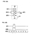
- the data latch circuit includes a clocked inverter 2005 and an inverter 2006.
- the clocked inverter 2005 includes P-channel TFTs 2001 and 2002 and N-channel TFTs 2003 and 2004 all connected in series.
- the gate electrode of the P-channel TFT 2001 is input with a sampling pulse (LAT) from a shift register while the source electrode have a connecting structure such that a power supply VDD is supplied.
- the gate electrode of the N-channel TFT 2004 is input with an inverted pulse (LATB) of the sampling pulse (LAT) while the source electrode have a connecting structure such that a power supply VSS is supplied.
- the gate electrodes of the P-channel TFT 2002 and the N-channel TFT 2003 are input with a digital signal (DATA).
- the drain electrodes of the P-channel TFT 2002 and the N-channel TFT 2003 are connected to the inverter 2006.
- FIG. 2(B) is a timing chart of the conventional data latch circuit in FIG. 2(A) . Operation of the conventional data latch circuit is described with reference to FIGS. 2(A) and 2(B) .
- a digital signal hereinafter referred to as a 'data signal'
- a digital signal to be input has a digital format, that is a signal having a potential representing '1' and a potential representing '0'.
- the level of the potential representing '1' is referred to as 'H level' and a potential representing '0' is referred to as 'L level' in any case, regardless of the potential.
- the potential level satisfies L level ⁇ H level unless specially described.
- the sampling pulse (LAT) at L level is input from a shift register. Then, the LAT is at L level and the LATB is at H level, turning ON the P-channel TFT 2001 and the N-channel TFT 2004. At this time, when the DATA is at H level, the P-channel TFT 2002 is turned OFF while the N-channel TFT 2003 is turned ON, thus the clocked inverter 2005 outputs VSS. On the other hand, when the DATA is at L level, the P-channel TFT 2002 is turned ON while the N-channel TFT 2003 is turned OFF, thus the clocked inverter 2005 outputs VDD.
- a sampling pulse, LAT is input from a shift register. Then, the LAT is at L level (-2V) while the LATB is at H level (5V), thereby turning ON the P-channel TFT 2001 and the N-channel 2004. At this time, when the DATA is at H level (3V), the P-channel TFT 2002 is turned OFF while the N-channel TFT 2003 is turned ON. Thus, the clocked inverter 2005 outputs VSS. At this time, however, if the threshold voltage
- the characteristics of the P-channel TFT 2002 and the N-channel TFT in particular, the threshold characteristics vary.
- 5 V, the logic is inverted, which causes the output of the clocked inverter 2005 to be at VDD, not VSS.
- the N-channel TFT 2003 is incidentally turned ON and thus a leakage current flows. Furthermore, when the ON current of the N-channel TFT 2003 at
- 2 V is larger than the ON current of the P-channel TFT 2002 at
- 5 V, the logic is inverted, which causes the output of the clocked inverter 2005 to be at VSS, not VDD.
- the invention is made in view of the foregoing problems and provides a data latch circuit which is hardly influenced by variations in the TFT characteristics, and capable of operating with low power consumption and high frequency.
- the data latch circuit of the invention having an inverter which determines a data signal to be at H level or at L level is constructed such that a means for short-circuiting an input terminal and an output terminal of the inverter is provided, the input terminal of the inverter is connected to one electrode of a capacitor, and the other electrode of the capacitor samples a data signal or a reference potential.
- the input terminal of the inverter and the one terminal of the capacitor are set at the threshold potential of the inverter, while the other electrode of the capacitor is set at the reference potential.
- the invention provides a data latch circuit which samples a digital signal includes:
- a data latch circuit which samples a digital signal includes:
- the first potential may be a potential of 1 or a potential of 0 as the digital signal.
- the amplitude of the digital signal may be set comperatively smaller than the width of a power supply voltage which is used for the data latch circuit.
- An output pulse from the shift register of the preceding stage may be used for a control terminal of the clocked inverter.
- the data latch circuit may be formed by using thin film transistors.
- an accurate operation can be obtained without being influenced by variations in the TFT characteristics even when the amplitude of an input signal is small relatively to the width of a power supply voltage. Therefore, signals from an external circuit are not required to be level shifted, and thus reduction in power consumption, layout area and cost can be achieved.
- FIG. 1(A) shows a configuration of a data latch circuit of an example not being part of the invention.
- the data latch circuit of this example includes a data sampling switch 1001, a reference switch 1002, a switch 1003 for setting the threshold value, a capacitor means 1004 and a correction inverter 1005.
- a circuit block including the data sampling switch 1001, the reference switch 1002 and the capacitor means 1004 is denoted by 'block x'.
- an inverter 1006 may be provided if necessary.
- ON/OFF of the data sampling switch 1001 is controlled by a LAT.
- DATA to be input is input to a connecting node (hereinafter referred to as a 'node a') of the reference switch 1002 and a second electrode of the capacitor means 1004.
- ON/OFF of the reference switch 1002 is controlled by a LAT-1.
- the reference switch 1002 samples a first potential (referred to as a 'reference potential' herein), and outputs the reference potential to a connecting node of the data sampling switch 1001 and the second electrode of the capacitor means 1004, namely the node a.
- An input terminal and an output terminal of the correction inverter 1005 are electrically connected through the switch 1003 for setting the threshold value.
- a 'node b' and a 'node c' Connecting nodes between the input terminal of the correction inverter 1005 and the switch 1003 for setting the threshold value and between the output terminal thereof and the switch 1003 for setting the threshold value are referred to as a 'node b' and a 'node c' respectively. ON/OFF of the switch 1003 for setting the threshold value is controlled by the LAT-1.
- the correction inverter 1005 outputs data to the inverter 1006 which is connected to the node c.
- FIG. 1(B) is a timing chart of the data latch circuit. Operation is described in the case where the data latch circuit is driven at a low voltage with reference to FIG. 1(A) and FIG. 1(B) . It is assumed that VSS is - 2 V, VDD is 5 V, H level of each of LAT, LATB, LAT-1 and LAT-1B is 5 V while L level thereof is - 2 V, H level of DATA is 3 V while L level thereof is 0 V, and a reference potential is 1.5 V which is an intermediate potential between the L level and the H level of the DATA. It is preferable that the LAT which is input during a period T1 does not overlap with the pulse LAT-1 which is input during a period T2.
- a sampling pulse LAT-1 (5 V) is input from a shift register of the preceding stage to the present data latch circuit, whereby the reference switch 1002 and the switch 1003 for setting the threshold value are turned ON.
- the node a is at a reference potential (1.5 V). Since the potential of the node c is feedbacked, the potential of the node b become unchanged, and the potential of the node b is at ' the threshold potential of the correction inverter 1005 (assumed to be 2 V here).
- the period T2 starts, in which the present data latch circuit determines the input DATA to be at H level or at L level.
- the sampling pulse LAT (5 V) from the shift register is input to the present data latch circuit, whereby the data sampling switch 1001 is turned ON.
- the input DATA is at H level (3 V)
- the potential of the node a changes from 1.5 V to 3 V.
- potential difference between both ends of the capacitor means 1004 is held, the potential of the node b changes by around the amount of voltage change at the node a. Accordingly, the potential of the node b is raised from 2 V by around 1.5 V, reaching around 3.5 V.
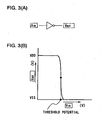
- FIGS. 3 show the V IN (input signal voltage)-V OUT (output signal voltage) characteristics of a general inverter. As shown in FIGS. 3 , when V IN changes higher or lower than the threshold value even by a small amount, V OUT draws closer to VDD or VSS to a large degree.
- the node c Since the node b is set at the threshold potential of the correction inverter 1005 in the period T1, the node c sensitively reacts to the change in potential of the node b. In this case, as the potential of the node b is raised from 2 V to around 3.5 V, the potential of the node c draws closer to VSS to a large degree. The potential of the node c is adjusted by the inverter 1006, and VDD (H level) is output to the output OUT.
- the potential of the node a drops from 1.5 V to 0 V
- the potential of the node b drops from 2 V by around 1.5 V, reaching around 0.5 V.
- the potential of the node c draws closer to VDD to a large degree.
- the potential of the node c is further adjusted by the inverter 1006, and VSS (L level) is output to the output OUT.
- the reference potential is a fixed potential, it is ideally an intermediate potential of an amplitude of the data signal (DATA here), however, it is not necessarily the intermediate potential in a strict sense.
- the reference potential can be changed to a degree within the amplitude of the data signal while being different from the highest potential or the lowest potential of the data signal.
- an inverted signal of the data signal DATA may be input as a reference potential after shifting it forth by one data.
- the node a when the DATA is at H level (3 V) for example, the node a is at L level (0 V) in the reset period T1, and when the DATA at H level (3 V) is input in the sampling period T2, the node a and the node b change by around 3 V, which facilitate the accurate operation of the correction inverter 1005.
- the node a is at H level (0 V)
- the DATA at L level (0 V) is input in the sampling period T2. Therefore, the node a and the node b change by around 3 V in a similar manner.
- the threshold potential of the inverter which outputs after determining the data signal DATA to be at H level or at L level is obtained in advance, and the data signal is determined to be at H level or L level based on its change whether being higher or lower than the threshold potential.
- an accurate operation can be obtained without being influenced by the threshold changes due to variations in the TFT characteristics even when the amplitude of an input signal is small relatively to the width of a power supply voltage. Therefore, low power consumption and high frequency operation are achieved.
- the invention is applied to a data latch circuit using polysilicon TFTs that have large variations in the TFT characteristics.
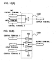
- holding may be carried out by using a clocked inverter 6002 or the like, or holding may be carried out by using a capacitor means 6003 or the like as shown in FIGS. 6(A) and 6(B) .
- a clocked inverter 6002 a general clocked inverter can be employed.
- a clocked inverter 10001 includes a first P-channel TFT 10002, a second P-channel TFT 10003, a first N-channel TFT 10004 and a second N-channel TFT 10005 all connected in series.
- a terminal which inputs to the gate electrode of the first P-channel TFT 10002 is a control terminal 1
- a terminal which inputs to the gate electrodes of the second P-channel TFT 10003 and the first N-channel TFT 10004 is an input terminal
- a terminal which inputs to the gate electrode of the second N-channel TFT 10005 is a control terminal 2
- a connecting terminal of the second P-channel TFT 10003 and the first N-channel TFT 10004 is an output terminal.
- FIG. 6(A) corresponds to FIG. 1(A) additionally provided with the capacitor means 6003 and the clocked inverter 6002.
- the clocked inverter 6002 is connected to an inverter 6001 in loop configuration.
- a holding pulse HOLD is input to a control terminal 1 of the clocked inverter 6002 while an inverted pulse HOLDB of the HOLD is input to a control terminal 2 thereof.
- the rest of the components arc similar to FIG. 1(A) .
- FIG. 6(B) corresponds to FIG. 1(A) additionally provided with a clocked inverter 6102.
- the clocked inverter 6102 is connected to a correction inverter 6101 in loop configuration.
- a holding pulse HOLD is input to a control terminal 1 of the clocked inverter 6102 while an inverted pulse HOLDB of the HOLD is input to a control terminal 2 thereof.
- the rest of the components are similar to FIG. 1(A) .
- the HOLD pulse is preferably a pulse such as 6201 and 6202 shown in the timing chart in FIG. 6(C) .
- An output pulse of a shift register may be employed for such pulse.
- H level and L level can be held accurately for a predetermined period.
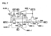
- FIG. 7 shows the case in which two blocks x in the data latch circuit in FIG. 1(A) are connected in parallel.
- One of two reference potentials which are input to the two reference switches respectively is set at the highest potential (potential having an equal level to the H level of the DATA) while the other is set at the lowest potential (potential having an equal level to the L level of the DATA).
- the data latch circuit in this embodiment mode includes a block y and a block y' connected in parallel, a correction inverter 7008 whose input terminal is connected to one of the connecting nodes of the block y and the block y', an inverter 7009 connected to the correction inverter 7008 in series, a switch 7007 for setting the threshold value connected between an input terminal and an output terminal of the correction inverter 7008, and a clocked inverter 7009.
- the block y includes a first data sampling switch 7001 and a first capacitor means 7005 connected in series, and a first reference switch 7003 for inputting a signal DH to their connecting node (hereinafter referred to as a 'node a').
- the block y' includes a second data sampling switch 7002 and a second capacitor means 7006 connected in series, and a second reference switch 7004 for inputting a signal DL to their connecting node (hereinafter referred to as a 'node a').
- ON/OFF of each of the first data sampling switch 7001 and the second data sampling switch 7002 is controlled by the LAT, thereby sampling the DATA.
- ON/OFF of each of the first reference switch 7003, the second reference switch 7004 and the switch 7007 for setting the threshold value is controlled by the LAT-1.
- the switch 7007 for setting the threshold value is provided between the input terminal and the output terminal of the correction inverter 7008.
- the connecting nodes between the input terminal of the correction inverter 7008 and the switch 7007 for setting the threshold value and between the output terminal of the correction inverter 7008 and the switch 7007 for setting the threshold value are referred to as a 'node b' and a 'node c' respectively.
- VSS is - 2 V
- VDD is 5 V
- H level of each of LAT, LATB, LAT-1 and LAT-1B is 5 V while L level thereof is 0 V
- H level of DATA (DH) is 3 V while L level thereof (DL) is 0 V.
- the timing chart in this embodiment is similar to the timing chart of Embodiment Mode 1 shown in FIG. 1(B) . Therefore, description is given here with reference to FIG. 1(B) .
- the LAT-1 is at H level (5 V), whereby the first reference switch 7003, the second reference switch 7004 and the switch 7007 for setting the threshold value are turned ON.
- the node a is at a potential of DH (3 V) while the node a' is at a potential of DL (0 V).
- the node b is at the threshold voltage (assumed to be 2 V here) of the correction inverter 7008.
- the LAT is at H level (5 V) and the LAT-1 is at L level (0 V).
- the first data sampling switch 7001 and the second data sampling switch 7002 are turned ON.
- the node a remains unchanged as 3 V while the node a' changes from 0 V to 3 V
- the node b is raised from 2 V by around 1.5 V, reaching 3.5 V.
- the node c draws closer to VSS (- 2 V) to a large degree.
- the node a changes from 3 V to 0 V while the node a' remains unchanged as 0 V.
- the node b drops from 2 V by around 1.5 V, reaching around 0.5 V. Accordingly, the node c draws closer to VDD (5 V) to a large degree.
- an accurate operation can be obtained without being influenced by the TFT characteristics even when the amplitude of an input signal is small relatively to the width of a power supply voltage. Therefore, low power consumption and high frequency operation can be achieved. Furthermore, according to the data latch circuit of this embodiment mode, by setting one of the two reference potentials, which are input to the two reference switches respectively, at the highest potential (DH) of the data signal while setting the other at the lowest potential (DL) of the data signal, an intermediate potential used for the reference potential is not particularly required, which contributes to the reduction in the number of power supplies.
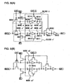
- the data latch circuit of the invention having a different configuration from those in Embodiment Mode 1 is shown in FIG. 8(A) .
- the data latch circuit of this embodiment mode includes a block z and a block z' connected in parallel, a first correction inverter 8001 whose input terminal is connected to one of the connecting nodes of the block z and the block z', an inverter 8002 connected to the first correction inverter 8001 in series, and a first switch 8003 for setting the threshold value provided between the input terminal and the output terminal of the first correction inverter 8001.
- the block z includes a first sampling switch 8004, a first capacitor means 8008, a second correction inverter 8010 and a third capacitor means 8012 all connected in series, a first reference switch 8006 for sampling the DH (potential having an equal level to the H level of DATA) to a connecting node (hereinafter referred to as a 'node a') of the first sampling switch 8004 and the first capacitor means 8008, and a second switch 8014 for setting the threshold value provided between an input terminal and an output terminal of the second correction inverter 8010.
- the block z' includes a second sampling switch 8005, a second capacitor means 8009, a third correction inverter 8011 and a fourth capacitor means 8013 all connected in series, a second reference switch 8007 for sampling the DL (potential having an equal level to the L level of DATA) to a connecting node (hereinafter referred to as a 'node a") of the second sampling switch 8005 and the second capacitor means 8009, and a third switch 8015 for setting the threshold value provided between an input terminal and an output terminal of the third correction inverter 8011.
- the DATA is input to the other connecting node of the block z and the block z', namely the connecting node of the first sampling switch 8004 and the second sampling switch 8005.
- ON/OFF of each of the first sampling switch 8004 and the second sampling switch 8005 is controlled by the LAT.
- ON/OFF of each of the first reference switch 8006, the second reference switch 8007, the second switch 8014 for setting the threshold value and the third switch 8015 for setting the threshold value is controlled by the LAT-1.
- Connecting nodes between the input terminal of the first correction inverter 8001 and the first switch 8003 for setting the threshold value and between the output terminal of the first correction inverter 8001 and the first switch 8003 for setting the threshold value are referred to as a 'node b' and a 'node c' respectively.
- Connecting nodes between the input terminal of the second correction inverter 8010 and the second switch 8014 for setting the threshold value and between the output terminal of the second correction inverter 8010 and the second switch 8014 for setting the threshold value are referred to as a 'node a2' and a 'node a3' respectively.
- the timing chart in this embodiment is similar to the timing chart of Embodiment Mode 1 shown in FIG. 1(B) . Therefore, operation is described with reference to FIG. 1(B) .
- the LAT-1 is at H level (VDD)
- the node a is at a potential of DH
- the node a' is at a potential of DL
- the node a2 and the node a3 are at the threshold potential of the second correction inverter 8010
- the node a2' and the node a3' are at the threshold potential of the third correction inverter 8011.
- the LAT is at H level (VDD) and the DATA is sampled.
- VDD H level
- the potentials of node a and the node a2 remain unchanged while the potential of the node a' changes from DL to H level and the potential of the node a2' is raised by the amount of amplitude of the DATA.
- the potential of the node a3' draws closer to VSS to a large degree and the potential of the node b drops. Accordingly, the potential of the node c draws closer to VDD to a large degree.
- the potentials of the node a' and the node a2' remain unchanged while the potential of the node a changes from DH to L level and the potential of the node a2 drops by the amount of amplitude of the DATA.
- the potential of the node a3 draws closer to VDD to a large degree while the potential of the node b is raised.
- the potential of the node c draws closer to VSS to a large degree.
- a fifth capacitor means 8016 is provided between the node a2 and the node a2' as shown in FIG. 8(B) .
- the capacitor means 8016 the potentials of the node a2 and the node a2' change in the same direction, preventing malfunction.
- an accurate operation can be obtained without being influenced by variations in the TFT characteristics even when the amplitude of an input signal is smaller than those of other Embodiment modes, relatively to the width of a power supply voltage. Therefore, low power consumption and high frequency operation are achieved. Furthermore, according to the data latch circuit of this embodiment mode, by setting one of the two reference potentials, which are input to the two reference switches respectively, at the highest potential (DH) of the data signal while setting the other at the lowest potential (DL) of the data signal, an intermediate potential used for the reference potential is not particularly required, which contributes to the reduction in the number of power supplies.
- Embodiment Modes 1 and 2 Although described heretofore in Embodiment Modes 1 and 2 is the case of employing an N-channel TFT for each of the data sampling switch, the reference switch, and the switch for setting the threshold value, all or some of them may be replaced by P-channel TFTs or analog switches having both N-channel and P-channel TFTs depending on the value of a power supply and a signal voltage or the amplitude of signals.
- a sampling pulse from the shift register of the preceding stage is used as the reset pulse LAT-1, it may a sampling pulse from the shift register on the several stages earlier, or a pulse may be input for resetting. Alternatively, all the stages may be reset at a time.
- the setting of the voltage is not limited to this as well.
- Described here is a configuration of an active matrix display device and its drive to which the data latch circuit of the invention is applied.
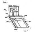
- FIG. 4 is a block diagram of an external circuit and a schematic view of a panel. Taken here as an example is an active matrix EL display device.
- the active matrix display device includes an external circuit 4004 and a panel 4010.
- the external circuit 4004 includes an A/D converting unit 4001, a power supply unit 4002, and a signal generating unit 4003.
- the A/D converting unit 4001 converts a video data signal input as an analog signal into a digital signal, and then supplies it to a source signal line driver circuit 4006.
- the power supply unit 4002 generates a power supply having a desired value of voltage from a power supply such as a battery and an outlet, and supplies it to the source signal line driver circuit 4006, gate signal line driver circuits 4007, an EL element 4011, the signal generating unit 4003 or the like.
- the signal generating unit 4003 is input with a power supply, a video signal, a synchronizing signal or the like and converts various signals as well as generating a clock signal or the like for driving the source signal line driver circuit 4006 and the gate signal line driver circuits 4007.
- the signal and power supply from the external circuit 4004 is input from an FPC connecting portion 4005 in the panel 4010 to the internal circuit, the EL element 4011 or the like through an FPC.
- the panel 4010 includes the FPC connecting portion 4005, the internal circuit, and the EL element 4011 over a glass substrate 4008.
- the internal circuit includes the source signal line driver circuit 4006, the gate signal line driver circuits 4007, and a pixel portion 4009.
- the pixel portion 4009 is disposed, and the source signal line driver circuit 4006 and the gate signal line driver circuits 4007 are disposed on its periphery.
- the EL element 4011 and a counter electrode of the EL element are formed over an entire surface of the pixel portion 4009.
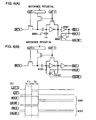
- FIG. 5 is a more detailed block diagram showing the source signal line driver circuit 4006.
- the source signal line driver circuit 4006 includes a shift register 5002 having a plurality of stages of D-flip flops (Delayed Flip-Flops; D-FFs) 5001, a data latch circuit 5003, a latch circuit 5004, a level shifter 5005, a buffer 5006 or the like.
- the data latch circuit of the invention can be applied to the data latch circuit 5003 portion.
- the data latch circuit described in any of Embodiment Modes can be adopted. Although the description is given here on the case where the invention is applied to the data latch circuit 5003, the data latch circuit may be applied to the latch circuit 5004 as well.
- Signals to be input are a clock signal line (S-CK), an inverted clock signal line (S-CKB), a start pulse (S-SP), a digital video signal (DATA), and a latch pulse (Latch Pulse).
- S-CK clock signal line
- S-CKB inverted clock signal line
- S-SP start pulse
- DATA digital video signal
- Latch Pulse latch pulse
- an intermediate potential of an amplitude of the digital video signal is input.
- a sampling pulse is output from the shift register 5002 in sequence according to the timing at which a clock signal, a clock inverted signal and a start pulse are input.
- the sampling pulse is input to the latch circuit 5004.
- the latch circuit 5004 is reset by the sampling pulse which is input from the D-FF 5001 of the preceding stage, and then samples a digital video signal at the timing at which a sampling pulse from the D-FF 5007 of the present stage is input, thereby holding it. This operation is performed from the first column in sequence.
- a latch pulse is input during a horizontal fly-back period.
- the digital video signals held in the data latch circuit 5003 are transferred to the latch circuit 5004 all at once.
- the signals are level shifted in the level shifter 5005, and then, after being adjusted by the buffer 5006, they are output to source signal lines S1 to Sn all at once.
- H level and L level are input to the pixels in the row selected by the gate signal line driver circuits 4007, thereby controlling light emission or non-light emission of the EL element 4011.
- the panel 4010 and the external circuit 4004 are separately provided in the active matrix display device in this embodiment, they may be integrated over the same substrate.
- organic EL is used as an example for the display device, a light emitting device using light emitting elements other than organic EL or a liquid crystal display device can be used as well.
- the source signal line driver circuit 4006 may be removed of the level shifter 5005 and the buffer 5006 as well.
- the data latch circuit of the invention can be used for various display devices, and the display devices can be used in the display portions of various electronic devices.
- the display device of the invention can be preferably used for mobile devices that require low power consumption.
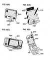
- the electronic devices include a mobile information device (mobile phone, mobile computer, portable game machine, an electronic book or the like), a video camera, a digital camera, a goggle type display, a display, a navigation system or the like. Specific examples of these electronic devices are shown in FIGS. 9(A) to 9(D) .
- FIG. 9(A) is a display including a housing 9001, an audio output portion 9002, a display portion 9003 or the like.
- the display device using the data latch circuit of the invention can be used for the display portion 9003.
- the display device includes all the information display devices for a personal computer, a TV broadcasting receiver, an advertisement display or the like.
- FIG. 9(B) is a mobile computer including a main body 9101, a stylus 9102, a display portion 9103, operating switches 9104, an external interface 9105 or the like.
- the display device using the data latch circuit of the invention can be used for the display portion 9103.
- FIG. 9(C) is a game machine including a main body 9201, a display portion 9202, operating switches 9203 or the like.
- the display device using the data latch circuit of the invention can be used for the display portion 9202.
- FIG. 9(D) is a mobile phone including a main body 9301, an audio output portion 9302, an audio input portion 9303, a display portion 9304, operating switches 9305, an antenna 9306 or the like.
- the display device using the data latch circuit of the invention can be used for the display portion 9304.
- the data latch circuit of the invention can be applied to all the circuits which sample digital data, and in particular, it is suitably applied to a driver circuit of a display device.
- the scope of application of the display device using the data latch circuit of the invention in a portion of its driver circuit is so wide that it can be used for display devices in various fields.
Landscapes
- Engineering & Computer Science (AREA)
- Physics & Mathematics (AREA)
- Computer Hardware Design (AREA)
- General Physics & Mathematics (AREA)
- Theoretical Computer Science (AREA)
- Microelectronics & Electronic Packaging (AREA)
- Power Engineering (AREA)
- Nonlinear Science (AREA)
- Control Of Indicators Other Than Cathode Ray Tubes (AREA)
- Liquid Crystal Display Device Control (AREA)
- Control Of El Displays (AREA)
- Logic Circuits (AREA)
- Electroluminescent Light Sources (AREA)
- Liquid Crystal (AREA)
Abstract
Claims (8)
- Circuit de verrouillage de données qui échantillonne un signal numérique, comportant:un premier moyen de condensateur (7005) ayant une première électrode et une seconde électrode,un second moyen de condensateur (7006) ayant une troisième électrode et une quatrième électrode,un premier inverseur (7008) comprenant un transistor dont une borne d'entrée est reliée à la première électrode et à la troisième électrode, etun premier interrupteur (7007) relié entre la borne d'entrée et une borne de sortie du premier inverseur (7008),dans lequel le circuit de verrouillage de données est caractérisé en ce quele premier interrupteur (7007) est programmé pour être fermé pendant que ledit circuit de verrouillage de données transmet un premier potentiel à la seconde électrode du premier moyen de condensateur (7005) et transmet un second potentiel à la quatrième électrode du second moyen de condensateur (7006) pendant une période de réinitialisation, dans lequel le premier potentiel est égal au niveau haut du signal numérique et le second potentiel est égal au niveau bas du signal numérique, et aussiledit circuit de verrouillage de données transmet le signal numérique à la seconde électrode du premier moyen de condensateur (7005) et à la quatrième électrode du second moyen de condensateur (7006) pendant une période d'échantillonnage après la période de réinitialisation.
- Circuit de verrouillage de données selon la revendication 1, comprenant aussi
un second interrupteur et un troisième interrupteur (7001, 7003) reliés à la seconde électrode, et un quatrième interrupteur et un cinquième interrupteur (7002, 7004) reliés à la quatrième électrode,
dans lequel le second interrupteur (7001) est programmé pour être fermé afin de transmettre le premier potentiel à la seconde électrode du premier moyen de condensateur (7005), et le quatrième interrupteur (7002) est programmé pour être fermé afin de transmettre le second potentiel à la quatrième électrode du second moyen de condensateur (7006) pendant la période de réinitialisation, et aussi le troisième
interrupteur (7003) est programmé pour être fermé afin de transmettre le signal numérique à la seconde électrode du premier moyen du condensateur (7005), et le cinquième interrupteur (7004) est programmé pour être fermé afin de transmettre le signal numérique à la quatrième électrode du second moyen de condensateur (7006) pendant la période d'échantillonnage après la période de réinitialisation. - Circuit de verrouillage de données qui échantillonne un signal numérique, comportant:un premier moyen de condensateur (8008) ayant une première électrode et une seconde électrode,un second moyen de condensateur (8012) ayant une troisième électrode et une quatrième électrode,un premier inverseur (8010) dont une borne d'entrée est reliée à la première électrode et dont une borne de sortie est reliée à la troisième électrode,un premier interrupteur (8014) relié entre la borne d'entrée et la borne de sortie du premier inverseur (8010),un troisième moyen de condensateur (8009) ayant une cinquième électrode et une sixième électrode,un quatrième moyen de condensateur (8013) ayant une septième électrode et huitième électrode,un second inverseur (8011) dont une borne d'entrée est reliée à la cinquième électrode et dont une borne de sortie est reliée à la septième électrode,un second interrupteur (8015) relié entre la borne d'entrée et la borne de sortie du second inverseur (8011),un troisième inverseur (8001) comprenant un transistor dont une borne d'entrée est reliée à la quatrième électrode et à la huitième électrode, etun troisième interrupteur (8003) relié entre la borne d'entrée et une borne de sortie du troisième inverseur (8001),dans lequel le circuit de verrouillage de données est caractérisé en ce que le premier interrupteur, le second interrupteur et le troisième interrupteur (8014, 8015, 8003) sont programmés pour être fermés pendant que ledit circuit de verrouillage de données transmet un premier potentiel à la seconde électrode du premier moyen de condensateur (8008), et transmet un second potentiel à la sixième électrode du troisième moyen de condensateur (8009) pendant une période de réinitialisation, dans lequel le premier potentiel est égal au niveau haut du signal numérique et le second potentiel est égal au niveau bas du signal numérique, et aussi
ledit circuit de verrouillage de données transmet le signal numérique à la seconde électrode du premier moyen de condensateur (8008) et à la sixième électrode du troisième moyen de condensateur (8009) pendant une période d'échantillonnage après la période de réinitialisation. - Circuit de verrouillage de données selon la revendication 3, comprenant aussi un sixième condensateur relié à la première électrode et à la cinquième électrode.
- Circuit de verrouillage de données selon l'une quelconque des revendications 1 à 4, dans lequel la période de réinitialisation est déterminée par une impulsion d'échantillonnage d'un registre à décalage dans l'étage précédant tandis que la période d'échantillonnage est déterminée par une impulsion d'échantillonnage d'un registre à décalage dans l'étage actuel.
- Circuit de verrouillage de données selon l'une quelconque des revendications 1 à 4, dans lequel l'amplitude du signal numérique est relativement faible par rapport à la largeur d'une tension d'alimentation utilisée pour le circuit de verrouillage de données.
- Circuit de verrouillage de données selon l'une quelconque des revendications 1 à 4, dans lequel le circuit de verrouillage de données est formé en utilisant des transistors en couche mince.
- Dispositif électronique utilisant le circuit de verrouillage de données selon l'une quelconque des revendications 1 à 4.
Applications Claiming Priority (3)
| Application Number | Priority Date | Filing Date | Title |
|---|---|---|---|
| JP2002351672 | 2002-12-03 | ||
| JP2002351672 | 2002-12-03 | ||
| PCT/JP2003/015385 WO2004051852A1 (fr) | 2002-12-03 | 2003-12-02 | Circuit a verrouillage de donnees et appareil electronique |
Publications (3)
| Publication Number | Publication Date |
|---|---|
| EP1569342A1 EP1569342A1 (fr) | 2005-08-31 |
| EP1569342A4 EP1569342A4 (fr) | 2008-06-04 |
| EP1569342B1 true EP1569342B1 (fr) | 2011-03-23 |
Family
ID=32463164
Family Applications (1)
| Application Number | Title | Priority Date | Filing Date |
|---|---|---|---|
| EP03776011A Expired - Lifetime EP1569342B1 (fr) | 2002-12-03 | 2003-12-02 | Circuit a verrouillage de donnees et appareil electronique |
Country Status (9)
| Country | Link |
|---|---|
| US (5) | US7142030B2 (fr) |
| EP (1) | EP1569342B1 (fr) |
| JP (2) | JP4841839B2 (fr) |
| KR (1) | KR101062241B1 (fr) |
| CN (1) | CN100365934C (fr) |
| AU (1) | AU2003284526A1 (fr) |
| DE (1) | DE60336501D1 (fr) |
| TW (1) | TW200500829A (fr) |
| WO (1) | WO2004051852A1 (fr) |
Families Citing this family (22)
| Publication number | Priority date | Publication date | Assignee | Title |
|---|---|---|---|---|
| US7142030B2 (en) * | 2002-12-03 | 2006-11-28 | Semiconductor Energy Laboratory Co., Ltd. | Data latch circuit and electronic device |
| US6870895B2 (en) * | 2002-12-19 | 2005-03-22 | Semiconductor Energy Laboratory Co., Ltd. | Shift register and driving method thereof |
| JP4007336B2 (ja) * | 2004-04-12 | 2007-11-14 | セイコーエプソン株式会社 | 画素回路の駆動方法、画素回路、電気光学装置および電子機器 |
| JP4551731B2 (ja) * | 2004-10-15 | 2010-09-29 | 株式会社東芝 | 半導体集積回路 |
| EP1717783B1 (fr) * | 2005-04-28 | 2015-06-03 | Semiconductor Energy Laboratory Co., Ltd. | Circuit fermé de données, procédé de commande du circuit fermé et dispositif d'affichage |
| US7675796B2 (en) * | 2005-12-27 | 2010-03-09 | Semiconductor Energy Laboratory Co., Ltd. | Semiconductor device |
| JP4954639B2 (ja) * | 2006-08-25 | 2012-06-20 | パナソニック株式会社 | ラッチ回路及びこれを備えた半導体集積回路 |
| US7764086B2 (en) * | 2006-12-22 | 2010-07-27 | Industrial Technology Research Institute | Buffer circuit |
| JP2010102299A (ja) * | 2008-09-25 | 2010-05-06 | Seiko Epson Corp | 電気泳動表示装置及びその駆動方法並びに電子機器 |
| JP2012256012A (ja) * | 2010-09-15 | 2012-12-27 | Semiconductor Energy Lab Co Ltd | 表示装置 |
| JP5859839B2 (ja) * | 2011-01-14 | 2016-02-16 | 株式会社半導体エネルギー研究所 | 記憶素子の駆動方法、及び、記憶素子 |
| TWI433101B (zh) * | 2011-04-21 | 2014-04-01 | Au Optronics Corp | 電泳顯示裝置及其畫面更新方法 |
| US9935622B2 (en) | 2011-04-28 | 2018-04-03 | Semiconductor Energy Laboratory Co., Ltd. | Comparator and semiconductor device including comparator |
| TWI525615B (zh) * | 2011-04-29 | 2016-03-11 | 半導體能源研究所股份有限公司 | 半導體儲存裝置 |
| US8736315B2 (en) * | 2011-09-30 | 2014-05-27 | Semiconductor Energy Laboratory Co., Ltd. | Semiconductor device |
| JP5856799B2 (ja) * | 2011-10-17 | 2016-02-10 | ピクストロニクス,インコーポレイテッド | ラッチ回路および表示装置 |
| JP6064313B2 (ja) * | 2011-10-18 | 2017-01-25 | セイコーエプソン株式会社 | 電気光学装置、電気光学装置の駆動方法および電子機器 |
| US8786319B1 (en) * | 2012-03-16 | 2014-07-22 | Applied Micro Circuits Corporation | Latch isolation circuit |
| JP6015095B2 (ja) * | 2012-04-25 | 2016-10-26 | セイコーエプソン株式会社 | 電気光学装置および電子機器 |
| US9160293B2 (en) | 2013-09-07 | 2015-10-13 | Robert C. Schober | Analog amplifiers and comparators |
| CN104092448B (zh) * | 2014-06-18 | 2017-05-31 | 京东方科技集团股份有限公司 | 比较器、显示基板和显示装置 |
| WO2019038618A1 (fr) | 2017-08-24 | 2019-02-28 | Semiconductor Energy Laboratory Co., Ltd. | Amplificateur de détection, dispositif à semi-conducteur, son procédé de fonctionnement et dispositif électronique |
Family Cites Families (33)
| Publication number | Priority date | Publication date | Assignee | Title |
|---|---|---|---|---|
| US4237390A (en) * | 1978-09-28 | 1980-12-02 | National Semiconductor Corporation | Switching comparator |
| JPS59126319A (ja) * | 1982-08-31 | 1984-07-20 | Toshiba Corp | チヨツパ形コンパレ−タ |
| US4547683A (en) * | 1982-10-18 | 1985-10-15 | Intersil, Inc. | High speed charge balancing comparator |
| JPS5997220A (ja) * | 1982-11-26 | 1984-06-05 | Nec Corp | 電圧比較回路 |
| EP0111230B1 (fr) * | 1982-11-26 | 1987-03-11 | Nec Corporation | Dispositif pour comparer des tensions |
| US4633222A (en) * | 1985-10-01 | 1986-12-30 | Rca Corporation | Clock shaping circuit and method |
| US4691189A (en) * | 1986-05-23 | 1987-09-01 | Rca Corporation | Comparator with cascaded latches |
| JPH0695635B2 (ja) | 1988-06-21 | 1994-11-24 | 日本電気株式会社 | レベルシフト回路 |
| JPH04264814A (ja) * | 1991-02-19 | 1992-09-21 | Mitsubishi Electric Corp | 半導体装置 |
| JP2743683B2 (ja) | 1991-04-26 | 1998-04-22 | 松下電器産業株式会社 | 液晶駆動装置 |
| US5262685A (en) * | 1991-10-16 | 1993-11-16 | Unitrode Corporation | High-speed, low power auto-zeroed sampling circuit |
| JPH0774638A (ja) * | 1993-08-31 | 1995-03-17 | Mitsubishi Electric Corp | A−d変換器 |
| JPH07273616A (ja) | 1994-03-29 | 1995-10-20 | Kawasaki Steel Corp | チョッパ型コンパレータ |
| JP3326014B2 (ja) * | 1994-07-14 | 2002-09-17 | 株式会社半導体エネルギー研究所 | 薄膜半導体装置 |
| FR2722625B1 (fr) * | 1994-07-18 | 1996-10-04 | Thomson Consumer Electronics | Convertisseur a/n a comparaison multiple utilisant le principe d'interpolation |
| JPH0983316A (ja) * | 1995-09-07 | 1997-03-28 | Sanyo Electric Co Ltd | コンパレータおよびアナログ−デジタル変換回路 |
| JPH1155087A (ja) * | 1997-07-29 | 1999-02-26 | Rohm Co Ltd | コンパレータ及びad変換回路 |
| JPH1185111A (ja) | 1997-09-10 | 1999-03-30 | Sony Corp | 液晶表示素子 |
| JPH11184432A (ja) | 1997-12-19 | 1999-07-09 | Sony Corp | 液晶表示装置の駆動回路 |
| JPH11184440A (ja) | 1997-12-25 | 1999-07-09 | Sony Corp | 液晶表示装置の駆動回路 |
| JP3585749B2 (ja) * | 1998-11-20 | 2004-11-04 | シャープ株式会社 | 半導体装置のシステム構成及びこの半導体装置のシステム構成を用いた液晶表示装置モジュール |
| JP3473745B2 (ja) | 1999-05-28 | 2003-12-08 | シャープ株式会社 | シフトレジスタ、および、それを用いた画像表示装置 |
| JP3698592B2 (ja) | 1999-07-12 | 2005-09-21 | 三菱電機株式会社 | 巻上機 |
| JP2002196732A (ja) | 2000-04-27 | 2002-07-12 | Toshiba Corp | 表示装置、画像制御半導体装置、および表示装置の駆動方法 |
| US7180496B2 (en) * | 2000-08-18 | 2007-02-20 | Semiconductor Energy Laboratory Co., Ltd. | Liquid crystal display device and method of driving the same |
| TW521249B (en) * | 2000-09-05 | 2003-02-21 | Toshiba Corp | Display apparatus and its driving method |
| JP3428593B2 (ja) | 2000-09-05 | 2003-07-22 | 株式会社東芝 | 表示装置及びその駆動方法 |
| JP4707858B2 (ja) | 2001-03-28 | 2011-06-22 | ソニー株式会社 | シフトレジスタおよびこれを用いた表示装置、ならびにカメラシステムおよび携帯端末装置 |
| GB2378066B (en) * | 2001-07-23 | 2005-10-26 | Seiko Epson Corp | Comparator circuit and method |
| JP3800050B2 (ja) * | 2001-08-09 | 2006-07-19 | 日本電気株式会社 | 表示装置の駆動回路 |
| JP2003179068A (ja) * | 2001-12-12 | 2003-06-27 | Hitachi Ltd | 画像表示装置およびその製造方法 |
| US7142030B2 (en) * | 2002-12-03 | 2006-11-28 | Semiconductor Energy Laboratory Co., Ltd. | Data latch circuit and electronic device |
| US6870895B2 (en) * | 2002-12-19 | 2005-03-22 | Semiconductor Energy Laboratory Co., Ltd. | Shift register and driving method thereof |
-
2003
- 2003-12-01 US US10/724,365 patent/US7142030B2/en not_active Expired - Fee Related
- 2003-12-02 KR KR1020057009014A patent/KR101062241B1/ko not_active Expired - Fee Related
- 2003-12-02 EP EP03776011A patent/EP1569342B1/fr not_active Expired - Lifetime
- 2003-12-02 DE DE60336501T patent/DE60336501D1/de not_active Expired - Lifetime
- 2003-12-02 CN CNB2003801050008A patent/CN100365934C/zh not_active Expired - Fee Related
- 2003-12-02 WO PCT/JP2003/015385 patent/WO2004051852A1/fr not_active Ceased
- 2003-12-02 AU AU2003284526A patent/AU2003284526A1/en not_active Abandoned
- 2003-12-02 JP JP2004531658A patent/JP4841839B2/ja not_active Expired - Fee Related
- 2003-12-02 TW TW092133896A patent/TW200500829A/zh not_active IP Right Cessation
-
2006
- 2006-11-27 US US11/563,451 patent/US7301382B2/en not_active Expired - Fee Related
-
2007
- 2007-10-24 US US11/877,730 patent/US8004334B2/en not_active Expired - Fee Related
-
2011
- 2011-06-03 JP JP2011125587A patent/JP5568510B2/ja not_active Expired - Fee Related
- 2011-08-19 US US13/213,483 patent/US8212600B2/en not_active Expired - Fee Related
-
2012
- 2012-06-29 US US13/537,229 patent/US8710887B2/en not_active Expired - Lifetime
Also Published As
| Publication number | Publication date |
|---|---|
| JP4841839B2 (ja) | 2011-12-21 |
| US20070085586A1 (en) | 2007-04-19 |
| EP1569342A1 (fr) | 2005-08-31 |
| JP2011239411A (ja) | 2011-11-24 |
| CN1720662A (zh) | 2006-01-11 |
| US8212600B2 (en) | 2012-07-03 |
| AU2003284526A1 (en) | 2004-06-23 |
| TW200500829A (en) | 2005-01-01 |
| US8004334B2 (en) | 2011-08-23 |
| US20080094340A1 (en) | 2008-04-24 |
| US8710887B2 (en) | 2014-04-29 |
| DE60336501D1 (de) | 2011-05-05 |
| EP1569342A4 (fr) | 2008-06-04 |
| US20040257136A1 (en) | 2004-12-23 |
| JPWO2004051852A1 (ja) | 2006-04-06 |
| WO2004051852A1 (fr) | 2004-06-17 |
| US7142030B2 (en) | 2006-11-28 |
| US20120262206A1 (en) | 2012-10-18 |
| KR101062241B1 (ko) | 2011-09-05 |
| KR20050072147A (ko) | 2005-07-08 |
| US7301382B2 (en) | 2007-11-27 |
| JP5568510B2 (ja) | 2014-08-06 |
| US20110304605A1 (en) | 2011-12-15 |
| TWI321714B (fr) | 2010-03-11 |
| CN100365934C (zh) | 2008-01-30 |
Similar Documents
| Publication | Publication Date | Title |
|---|---|---|
| US8212600B2 (en) | Data latch circuit and electronic device | |
| KR100832252B1 (ko) | 펄스 출력 회로 | |
| US8526568B2 (en) | Shift register and driving method thereof | |
| US7535259B2 (en) | Clocked inverter, NAND, NOR and shift register | |
| JP2009022021A (ja) | 半導体装置 | |
| US7307463B2 (en) | Source follower, voltage follower, and semiconductor device | |
| US7358789B2 (en) | Level shifter for display device | |
| US7688107B2 (en) | Shift register, display device, and electronic device | |
| JP4974512B2 (ja) | 半導体装置、表示装置及び電子機器 |
Legal Events
| Date | Code | Title | Description |
|---|---|---|---|
| PUAI | Public reference made under article 153(3) epc to a published international application that has entered the european phase |
Free format text: ORIGINAL CODE: 0009012 |
|
| 17P | Request for examination filed |
Effective date: 20050530 |
|
| AK | Designated contracting states |
Kind code of ref document: A1 Designated state(s): AT BE BG CH CY CZ DE DK EE ES FI FR GB GR HU IE IT LI LU MC NL PT RO SE SI SK TR |
|
| AX | Request for extension of the european patent |
Extension state: AL LT LV MK |
|
| DAX | Request for extension of the european patent (deleted) | ||
| RBV | Designated contracting states (corrected) |
Designated state(s): DE FI FR GB NL |
|
| A4 | Supplementary search report drawn up and despatched |
Effective date: 20080507 |
|
| 17Q | First examination report despatched |
Effective date: 20081117 |
|
| GRAP | Despatch of communication of intention to grant a patent |
Free format text: ORIGINAL CODE: EPIDOSNIGR1 |
|
| GRAS | Grant fee paid |
Free format text: ORIGINAL CODE: EPIDOSNIGR3 |
|
| GRAA | (expected) grant |
Free format text: ORIGINAL CODE: 0009210 |
|
| AK | Designated contracting states |
Kind code of ref document: B1 Designated state(s): DE FI FR GB NL |
|
| REG | Reference to a national code |
Ref country code: GB Ref legal event code: FG4D |
|
| REF | Corresponds to: |
Ref document number: 60336501 Country of ref document: DE Date of ref document: 20110505 Kind code of ref document: P |
|
| REG | Reference to a national code |
Ref country code: DE Ref legal event code: R096 Ref document number: 60336501 Country of ref document: DE Effective date: 20110505 |
|
| REG | Reference to a national code |
Ref country code: NL Ref legal event code: VDEP Effective date: 20110323 |
|
| PG25 | Lapsed in a contracting state [announced via postgrant information from national office to epo] |
Ref country code: FI Free format text: LAPSE BECAUSE OF FAILURE TO SUBMIT A TRANSLATION OF THE DESCRIPTION OR TO PAY THE FEE WITHIN THE PRESCRIBED TIME-LIMIT Effective date: 20110323 |
|
| PG25 | Lapsed in a contracting state [announced via postgrant information from national office to epo] |
Ref country code: NL Free format text: LAPSE BECAUSE OF FAILURE TO SUBMIT A TRANSLATION OF THE DESCRIPTION OR TO PAY THE FEE WITHIN THE PRESCRIBED TIME-LIMIT Effective date: 20110323 |
|
| PLBE | No opposition filed within time limit |
Free format text: ORIGINAL CODE: 0009261 |
|
| STAA | Information on the status of an ep patent application or granted ep patent |
Free format text: STATUS: NO OPPOSITION FILED WITHIN TIME LIMIT |
|
| PGFP | Annual fee paid to national office [announced via postgrant information from national office to epo] |
Ref country code: FR Payment date: 20111219 Year of fee payment: 9 |
|
| 26N | No opposition filed |
Effective date: 20111227 |
|
| REG | Reference to a national code |
Ref country code: DE Ref legal event code: R097 Ref document number: 60336501 Country of ref document: DE Effective date: 20111227 |
|
| GBPC | Gb: european patent ceased through non-payment of renewal fee |
Effective date: 20121202 |
|
| REG | Reference to a national code |
Ref country code: FR Ref legal event code: ST Effective date: 20130830 |
|
| PG25 | Lapsed in a contracting state [announced via postgrant information from national office to epo] |
Ref country code: GB Free format text: LAPSE BECAUSE OF NON-PAYMENT OF DUE FEES Effective date: 20121202 Ref country code: FR Free format text: LAPSE BECAUSE OF NON-PAYMENT OF DUE FEES Effective date: 20130102 |
|
| PGFP | Annual fee paid to national office [announced via postgrant information from national office to epo] |
Ref country code: DE Payment date: 20191119 Year of fee payment: 17 |
|
| REG | Reference to a national code |
Ref country code: DE Ref legal event code: R119 Ref document number: 60336501 Country of ref document: DE |
|
| PG25 | Lapsed in a contracting state [announced via postgrant information from national office to epo] |
Ref country code: DE Free format text: LAPSE BECAUSE OF NON-PAYMENT OF DUE FEES Effective date: 20210701 |