EP1560296A1 - Connection structure between circuit board and flexible board - Google Patents
Connection structure between circuit board and flexible board Download PDFInfo
- Publication number
- EP1560296A1 EP1560296A1 EP05250388A EP05250388A EP1560296A1 EP 1560296 A1 EP1560296 A1 EP 1560296A1 EP 05250388 A EP05250388 A EP 05250388A EP 05250388 A EP05250388 A EP 05250388A EP 1560296 A1 EP1560296 A1 EP 1560296A1
- Authority
- EP
- European Patent Office
- Prior art keywords
- flexible board
- casing
- circuit board
- contact
- insertion hole
- Prior art date
- Legal status (The legal status is an assumption and is not a legal conclusion. Google has not performed a legal analysis and makes no representation as to the accuracy of the status listed.)
- Withdrawn
Links
Images


Classifications
-
- H—ELECTRICITY
- H01—ELECTRIC ELEMENTS
- H01R—ELECTRICALLY-CONDUCTIVE CONNECTIONS; STRUCTURAL ASSOCIATIONS OF A PLURALITY OF MUTUALLY-INSULATED ELECTRICAL CONNECTING ELEMENTS; COUPLING DEVICES; CURRENT COLLECTORS
- H01R12/00—Structural associations of a plurality of mutually-insulated electrical connecting elements, specially adapted for printed circuits, e.g. printed circuit boards [PCB], flat or ribbon cables, or like generally planar structures, e.g. terminal strips, terminal blocks; Coupling devices specially adapted for printed circuits, flat or ribbon cables, or like generally planar structures; Terminals specially adapted for contact with, or insertion into, printed circuits, flat or ribbon cables, or like generally planar structures
- H01R12/70—Coupling devices
- H01R12/77—Coupling devices for flexible printed circuits, flat or ribbon cables or like structures
- H01R12/79—Coupling devices for flexible printed circuits, flat or ribbon cables or like structures connecting to rigid printed circuits or like structures
-
- H—ELECTRICITY
- H01—ELECTRIC ELEMENTS
- H01R—ELECTRICALLY-CONDUCTIVE CONNECTIONS; STRUCTURAL ASSOCIATIONS OF A PLURALITY OF MUTUALLY-INSULATED ELECTRICAL CONNECTING ELEMENTS; COUPLING DEVICES; CURRENT COLLECTORS
- H01R12/00—Structural associations of a plurality of mutually-insulated electrical connecting elements, specially adapted for printed circuits, e.g. printed circuit boards [PCB], flat or ribbon cables, or like generally planar structures, e.g. terminal strips, terminal blocks; Coupling devices specially adapted for printed circuits, flat or ribbon cables, or like generally planar structures; Terminals specially adapted for contact with, or insertion into, printed circuits, flat or ribbon cables, or like generally planar structures
- H01R12/70—Coupling devices
- H01R12/82—Coupling devices connected with low or zero insertion force
- H01R12/85—Coupling devices connected with low or zero insertion force contact pressure producing means, contacts activated after insertion of printed circuits or like structures
- H01R12/89—Coupling devices connected with low or zero insertion force contact pressure producing means, contacts activated after insertion of printed circuits or like structures acting manually by moving connector housing parts linearly, e.g. slider
-
- H—ELECTRICITY
- H01—ELECTRIC ELEMENTS
- H01R—ELECTRICALLY-CONDUCTIVE CONNECTIONS; STRUCTURAL ASSOCIATIONS OF A PLURALITY OF MUTUALLY-INSULATED ELECTRICAL CONNECTING ELEMENTS; COUPLING DEVICES; CURRENT COLLECTORS
- H01R4/00—Electrically-conductive connections between two or more conductive members in direct contact, i.e. touching one another; Means for effecting or maintaining such contact; Electrically-conductive connections having two or more spaced connecting locations for conductors and using contact members penetrating insulation
- H01R4/28—Clamped connections, spring connections
- H01R4/50—Clamped connections, spring connections utilising a cam, wedge, cone or ball also combined with a screw
- H01R4/5083—Clamped connections, spring connections utilising a cam, wedge, cone or ball also combined with a screw using a wedge
Definitions
- the present invention relates to a flexible board connector for electrically connecting a flexible board to a circuit board to each other, and to a connection structure between a circuit board and a flexible board.
- connection strength is relatively weak.
- the holding member 74 is poor in versatility. This causes increase of cost. Further, the holding member 74 covers a much larger portion of the flexible board 72 in area than the portion where the signal terminal 78 is formed. Also, the holding member 74 has the plate spring 75 and the protrusion 76 in its inside. Moreover the holding member 74 is placed so as to protrude onto the circuit board 71. As a result, these make it difficult to downsize the components.
- An object of the present invention is therefore to provide a connector for use in flexible boards, the connector being downsized and thinned without any deterioration in strength or performance.
- the present invention provides a flexible board connector comprising:
- the outside contact portion of the contact protrudes from proximity to the upper end of the side surface of the casing.
- the inside contact portion of the contact defines the insertion hole together with the clamp surface of the clamp means. Therefore, for example, by connecting the outside contact portion to a terminal or the like formed on the surface of the circuit board and by inserting and clamping a portion of the flexible board into the insertion hole, the terminal formed at the portion of the flexible board can be connected to the inside contact portion.
- the circuit board and the flexible board can be electrically and mechanically connected to each other reliably.
- the terminal and the outside contact portion can be connected to each other by placing the casing into the hole of the circuit board, on the surface of which terminals or the like are formed. Thereby, the overall thickness of the circuit board and the flexible board connector is prevented from significantly increasing. As a consequence, downsizing of electronic equipment or the like using the flexible board connector can effectively be achieved.
- an opening of the insertion hole is positioned in proximity to the upper end of the side surface of the casing.
- the portion of the flexible board can easily and securely be inserted into the insertion hole under the condition that the casing is placed, for example, inside the hole of the circuit board.
- the opening of the insertion hole is formed in an upper surface of the casing in proximity to the upper end of the side surface of the casing.
- the portion of the flexible board can easily and securely be inserted into the insertion hole even under the condition that the whole casing is placed inside the hole of the circuit board.
- an outer peripheral surface of the casing is generally cup-like shaped, and the insertion hole is oriented to an oblique direction with respect to a bottom surface of the casing.
- the insertion hole is oriented oblique to the bottom surface of the casing, a size necessary for the insertion hole to accommodate the portion of the flexible board is effectively reduced in a direction parallel to the bottom surface of the casing. As a consequence, the flexible board connector can effectively be downsized.
- the clamp means has a holding portion for bending a non-clamp portion of the clamped flexible board to a particular direction.
- a portion of the flexible board placed inside the insertion hole is clamped by the clamp means.
- non-clamp portion of the flexible board is bent in a particular direction by the holding portion of the clamp means.
- the non-clamp portion of the flexible board can be bent in such a direction as not to significantly protrude from the surface of the casing. Accordingly, the circuit board and the flexible board which are connected to each other by this flexible board connector can effectively be downsized.
- connection structure between circuit board and flexible board comprising:
- the outside contact portion is positioned in proximity to the upper end of the side surface of the casing, while the connecting terminal is formed in proximity to the hole in the circuit board. Therefore, under the condition that at least the portion of the casing is placed inside the hole, the outside contact portion of this flexible board connector and the connecting terminal of the circuit board are easily and securely connected to each other. As a result, the portion of the flexible board connector protruding from the surface of the circuit board is lessened, the overall thickness of the circuit board and the flexible board connector as a whole can effectively be prevented from significantly increasing. Thus, electronic equipment, when made up by using this flexible board connector, can effectively be downsized.
- the portion of the flexible board is positioned within the insertion hole of the flexible board connector and clamped by the clamp means, the flexible board and the circuit board are mechanically and electrically connected to each other effectively via the flexible board connector.
- the flexible board connector of this constitution is applicable to different flexible boards and circuit boards by forming the arrangement that the outside contact portion into a shape corresponding to the connecting terminal of the circuit board, and by forming the inside contact portion into a shape corresponding to the connecting terminal of the flexible board. That is, only by changing the shape of the contacts, the flexible board connector becomes applicable to different flexible boards and circuit boards, hence high versatility, so that the manufacturing cost can be reduced.
- the flexible board connector is effectively downsized since the casing has only to be formed into enough dimensions to accommodate the portion of the flexible board.
- the opening of the insertion hole of the flexible board connector is positioned in an upper surface of the casing in proximity to the upper end of the side surface of the casing, an outer peripheral surface of the casing of the flexible board connector is generally cup-like shaped, and the insertion hole is oriented to an oblique direction with respect to a bottom surface of the casing, the clamp means of the flexible board connector has a holding portion, and a portion of the flexible board located outside the insertion hole is bent by the holding portion of the clamp means of the flexible board connector so as to be oriented substantially parallel to a top surface of the circuit board.
- the flexible board is partly positioned within the insertion hole of the flexible board connector, while the portion of the flexible board positioned outside the insertion hole is bent by the holding portion of the clamp means of the flexible board connector.
- the bent portion of the flexible board is oriented substantially parallel to the top surface of the circuit board, and therefore, positioned at a position close to the flexible board connector and the surface of the circuit board. That is, the portion of the flexible board outside the flexible board connector is prevented from significantly protruding from the flexible board connector or the circuit board. Accordingly, it is possible to effectively downsize the circuit board and the flexible board connected to each other by this flexible board connector. As a result, it is possible to effectively downsize electronic equipment or the like using this connection structure between circuit board and flexible board.
- the hole of the circuit board is a through-hole passing through the circuit board.
- the casing is placed inside the through-hole of the circuit board. Therefore, even with a relatively small thickness of the circuit board, the casing can be placed to the circuit board, for example, in such a state as to be almost never protruded from the surface of the circuit board. As a result, the whole connection structure between circuit board and flexible board can effectively be thinned.
- the hole of the circuit board is a non-through-hole having a depth smaller than thickness of the circuit board.
- the casing is placed inside the non-through-hole of the circuit board. For instance, by making the depth of the non-through-hole generally equal to the thickness of the casing, the casing is placed to the circuit board so as to be not protruded from any surfaces of the circuit board. As a result, the overall thickness of the flexible board connector and the circuit board is effectively be thinned.
- the bottom portion of the casing placed in the non-through-hole is not exposed in the rear surface of the circuit board because the hole of the circuit board is a non-through-hole. Accordingly, there is no fear that the casing may be protruded toward the top surface side of the circuit board or fall off due to a force derived from the rear surface side of the circuit board. Thus, the circuit board and the flexible board are stably connected to each other.
- the flexible board connector includes a casing, a contact having an outside contact portion protruding from proximity to an upper end of a side surface of the casing, and clamp means.
- the clamp means is at least partly placed within the casing and movable relative to the casing.
- the clamp means has a clamp surface that defines an insertion hole together with the inside contact portion of the contact. Further, the clamp means makes it possible to narrow the insertion hole by moving relative to the casing.
- the casing of the flexible board connector is placed in the hole of the circuit board, and the flexible board is electrically and mechanically fixed by being partly inserted into the insertion hole of the connector, by which the overall thickness of the circuit board, the connector and the flexible board can be reduced as compared with the prior art.
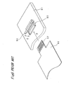
- Fig. 1 is a perspective view showing a flexible board connector according to an embodiment of the present invention.
- the flexible board connector 1 fixes a flexible board 30 to a circuit board 40 and electrically connects wiring of the flexible board 30 to circuits of the circuit board 40.
- the flexible board connector 1 has a generally rectangular parallelepiped casing 2, where the casing 2 is placed in a generally rectangular through-hole 41 formed in the circuit board 40.
- the casing 2 has an upper end portion protruded from a top surface of the circuit board 40.
- the flexible board connector 1 includes a plurality of conductive first and second contacts 3, 4 to electrically connect a circuit of the circuit board 40 to interconnect pattern as wiring of the flexible board 30.
- the first and second contacts 3, 4 have inside contact portions 3a, 4a located inside the casing 2, and a outside contact 3b, 4b located outside the casing 2. That is, an outside contact portion 3b of the first contact 3 protrudes from a side surface 23 which is a side surface portion of the casing 2 protruding from the top surface of the circuit board 40 and which extends along the lengthwise direction of the casing. Also, an outside contact portion 4b of the second contact 4 protrudes from a side surface 24 which is opposed to the side surface 23 from which the first contact 3 protrudes.
- the plural first and second contacts 3, 4 are, in either case, arrayed in parallel to each other to extend along the longitudinal direction of the casing 2.
- the outside contact portion 3b of the first contact 3 and the outside contact portion 4b of the second contact 4 are electrically and mechanically connected by means of solder to connecting terminals 43, 44, respectively, formed near the through-hole 41 of the circuit board 40.
- the casing 2 has an opening 6 in an upper side surface thereof, the opening 6 being near an upper end of the side surface of the casing 6.
- the opening 6 is provided in proximity to the side surface 23 from which the outside contact portion 3b of the first contact 3 protrudes.
- the opening 6 continues into an insertion hole formed within the casing 2.
- the opening 6 is so formed that a connecting portion 31 of the flexible board 30 is inserted hereinto.
- the opening 6 has a rectangular shape of longitudinally extending at the upper side surface of the casing 2.
- the protruding portion of the casing 2 from the top surface of the circuit board is mostly covered with an upper portion of a press member 8 which serves as clamp means.
- the upper portion of the press member 8 has a rectangular shape in a plain view.
- the longer side of the press member 8 is formed so as to have a length generally equal to the longitudinal length of the casing 2.
- the shorter side of the upper portion of the press member 8 continues into a support portion thereof which extends toward a bottom portion of the casing 2.
- an engagement claw is formed on an inner side surface of the support portion.
- This engagement claw is engaged with a guide groove 26 formed in the lateral side surface of the casing 2 so that the press member 8 can be moved along the guide groove 26 in the lateral direction as shown by arrow "A."
- a cover portion 8a is formed along a longer side verge of the upper portion of the press member 8. The cover portion 8a is positioned above the opening 6 of the upper side surface of the casing 2 when the press member 8 moves toward the side surface 23 of the casing 2.
- Fig. 2 is a view showing a state in which the flexible board connector 1 placed on the circuit board 40 is cut laterally.
- the inside contact portions 3a, 4a of the first and second contacts 3, 4 are respectively placed in the casing 2.
- the inside contact portion 3a of the first contact 3 is positioned on a slant along a sloped surface formed in an inner surface of the casing 2.
- a fixing portion 3c is connected between the inside contact portion 3a and the outside contact portion 3b of the first contact 3.
- the fixing portion 3c extends toward the bottom portion of the casing 2 and is fitted to a fixing hole formed in the casing 2.
- the second contact 4 has a vertical portion 4c adjoining the outside contact portion 4b.
- the vertical portion 4c extends along a vertically extending inner surface of the casing 2 toward its bottom.
- the inside contact portion 4a extends from the vertical portion 4c toward the opening 6 of the casing 2.
- a contact terminal 3d which has gradually increasing thickness.
- a contact terminal 4d which has gradually increasing thickness.
- the contact terminals 3d, 4d of the first and second contacts are placed close to each other.
- an insertion hole 9 is formed by a clamp surface 8b, which is the lower side surface of the press member 8, and the inside contact portions 3a, 4a of the first and second contacts 3, 4.
- the insertion hole 9, which continues to the opening 6 of the upper side surface of the casing 2, is inclined with respect to the bottom surface of the casing 2.
- a slide member 8c is located under the insertion hole 9.
- the slide member 8c is formed integrally with the press member 8 to move along with the press member 8.
- an inclined surface which is inclined downward so as to be oriented toward the first contact 3, as viewed in a lateral cross section of the connector.
- a wedge-shaped push-up block 10 is placed between the slide member 8c and the insertion hole 9.
- a surface of the push-up block 10 which surface makes contact with the slide member 8c is an inclined surface which is inclined downward toward the first contact 3.
- another surface of the push-up block 10 on the side of the insertion hole 9 is an inclined surface which is inclined upward toward the first contact 3.
- the surface of the push-up block 10 on the side of the insertion hole 9 is generally parallel and close to lower faces of the inside contact portions 3a, 4a of the first and second contacts 3, 4.
- the flexible board connector 1 having the above-stated construction connects the flexible board 30 to the circuit board 40 in the following manner.
- the press member 8 is moved toward the second contact 4 so that the opening 6 is exposed.
- the slide member 8c moves toward the second contact 4 along with the press member 8.
- the push-up block 10 whose lower surface is in contact with the inclined upper surface of the slide member 8c moves toward the bottom surface of the casing 2.
- the connecting portion 31 of the flexible board is inserted into the casing 2 through the exposed opening 6.
- the connecting portion 31 of the flexible board inserted into the casing 2 is positioned in the insertion hole 9 formed between the clamp surface 8b of the press member 8 and the inside contact portions 3a, 4a of the first and second contacts 3, 4.
- the connecting portion 31 of the flexible board 30 has its fore end 33 which is brought into contact with the clamp surface 8b by weight of the flexible board 30 outside of the connector 1.
- the press member 8 is moved toward the first contact 3 as shown in Fig. 4.
- the clamp surface 8b of the press member 8 presses the flexible board 30 downwardly.
- the push-up block 10 is moved upwardly by the slide member 8c moving toward the first contact 3 along with the press member 8. Consequently, the upper surface of the push-up block 10 presses the inside contact portions 3a, 4a of the first and second contacts 3, 4 upwardly.
- the insertion hole 9 is narrowed so that a portion of the flexible board 30 and the inside contact portions 3a, 4a of the first and second contacts 3, 4 are sandwiched between the clamp surface 8b of the press member 8 and the upper surface of the push-up block 10.
- the connecting portion 31 of the flexible board 30 and the contact terminals 3d, 4d of the first and second contacts 3, 4 are securely brought into contact with each other so as to be electrically and mechanically connected to each other.
- the cover portion 8a of the press member 8 When the press member 8 moves toward the first contact 3, the cover portion 8a of the press member 8 is positioned above the opening 6 of the casing 2. When this occurs, the press member 8 slides in the state that the press member 8 is fitted to the groove of the casing 2. Thereby, the cover portion 8a of the press member 8 causes the portion of the flexible board 30 located outside the insertion hole 9 of the casing 2 to be bent toward the upper surface of the casing 2. As a result, the portion of the flexible board 30 located outside the insertion hole 9 is oriented along a direction generally parallel to the surface of the circuit board 40.
- connection structure between the flexible board and the circuit board according to the present invention is obtained.
- the portion of the flexible board 30 located outside the insertion hole 9 is oriented along the direction generally parallel to the surface of the circuit board 40, such disadvantages as shown below can be prevented. That is, in the case where the flexible board 30 is inserted obliquely into the connector 1, the portion of the flexible board 30 located outside the insertion hole 9 bends to draw an arc as shown in Fig. 3 because the flexible board 30 has some degree of stiffness as well as flexibility. The stiffness of the flexible board 30 may allow this arc- portion of the flexible board 30 to protrude to a large extent from the surface of the circuit board 40.
- the portion of the flexible board 30 located outside the insertion hole 9 is bent to the direction generally parallel to the surface of the circuit board 40 by the cover portion 8a of the press member 8, as shown in Fig. 4.
- the flexible board 30 can effectively be prevented from protruding from the surface of the circuit board 40. Therefore, the flexible board 30 can effectively be prevented from such disadvantages as being disconnected from the connector or being damaged.
- the flexible board connector 1 in this embodiment include the plural first and second contacts 3, 4, the flexible board connector 1 may include only either one of the first contact 3 or the second contact 4.
- a dummy outside contact portion is preferably formed at a position on a side surface of the casing 2 which position corresponds to the outside contact portion of the other contact.
- the casing 2 can stably be fixed to the circuit board 40 when one of the outside contact portions 3b, 4b of the first and second contacts 3, 4 is fixed to one of terminals 43, 44 of the circuit board 40 and the dummy outside contact portion is fixed to the surface of the circuit board 40.
- the casing 2 of the flexible board connector 1 in this embodiment is placed in the through-hole 41 of the circuit board 40, the casing 2 may be placed in a non-through-hole which is provided in the circuit board and has a depth shallower than the thickness of the circuit board. In this case, the bottom surface of the casing 2 is not exposed in the rear side surface of the circuit board. Therefore, such disadvantages as protrusion or disconnection of the casing 2 can be prevented even if some force is exerted from the rear surface side of the circuit board.
- the portion of the casing 2 is placed within the through-hole 41 in the flexible board connector 1 of this embodiment, the entire casing may be placed within the through-hole.
- the flexible board connector can be made almost never protruding from the circuit board 40.
- the first and second contacts may be drawn outside from the upper side surface of the casing.
- the push-up block 10 in the casing 2 may be omitted. That is, the insertion hole 9 may be narrowed only by the press member 8.
Landscapes
- Coupling Device And Connection With Printed Circuit (AREA)
Applications Claiming Priority (2)
| Application Number | Priority Date | Filing Date | Title |
|---|---|---|---|
| JP2004023133A JP4121465B2 (ja) | 2004-01-30 | 2004-01-30 | フレキシブル基板用コネクタおよび回路基板とフレキシブル基板との接続構造 |
| JP2004023133 | 2004-01-30 |
Publications (1)
| Publication Number | Publication Date |
|---|---|
| EP1560296A1 true EP1560296A1 (en) | 2005-08-03 |
Family
ID=34650845
Family Applications (1)
| Application Number | Title | Priority Date | Filing Date |
|---|---|---|---|
| EP05250388A Withdrawn EP1560296A1 (en) | 2004-01-30 | 2005-01-26 | Connection structure between circuit board and flexible board |
Country Status (6)
| Country | Link |
|---|---|
| US (1) | US7025613B2 (zh) |
| EP (1) | EP1560296A1 (zh) |
| JP (1) | JP4121465B2 (zh) |
| KR (1) | KR100721071B1 (zh) |
| CN (1) | CN100373702C (zh) |
| TW (1) | TWI252609B (zh) |
Cited By (1)
| Publication number | Priority date | Publication date | Assignee | Title |
|---|---|---|---|---|
| EP2546932A3 (en) * | 2011-07-15 | 2015-06-24 | Hosiden Corporation | Terminal box and terminal box fixing arrangement |
Families Citing this family (17)
| Publication number | Priority date | Publication date | Assignee | Title |
|---|---|---|---|---|
| JP4014575B2 (ja) * | 2004-03-29 | 2007-11-28 | シャープ株式会社 | フレキシブル基板用コネクタ付き回路基板および回路基板とフレキシブル基板との接続構造 |
| TWI449281B (zh) * | 2006-04-25 | 2014-08-11 | Wago Verwaltungs Gmbh | Electronic connector |
| JP5073572B2 (ja) * | 2008-04-25 | 2012-11-14 | タイコエレクトロニクスジャパン合同会社 | 電気コネクタ |
| CN101645556B (zh) * | 2008-08-06 | 2011-12-28 | 和硕联合科技股份有限公司 | 连接器结构 |
| US7581975B1 (en) * | 2008-12-08 | 2009-09-01 | Cheng Uei Precision Industry Co., Ltd. | Flexible printed circuit connector |
| JP5600523B2 (ja) * | 2010-08-27 | 2014-10-01 | 矢崎総業株式会社 | コネクタ構造 |
| CN101964399B (zh) * | 2010-09-26 | 2013-04-17 | 东莞新能源科技有限公司 | 锂离子电池单体的极耳保护夹 |
| US8430684B1 (en) * | 2011-08-04 | 2013-04-30 | George F. Glatts, III | Ribbon cable connector |
| JP5959212B2 (ja) * | 2012-01-27 | 2016-08-02 | 日本圧着端子製造株式会社 | コネクタ |
| KR101920623B1 (ko) * | 2012-01-30 | 2018-11-21 | 삼성전자주식회사 | 신호케이블, 케이블커넥터 및 이를 포함하는 신호케이블 연결장치 |
| JP6272660B2 (ja) | 2013-05-17 | 2018-01-31 | スリーエム イノベイティブ プロパティズ カンパニー | コネクタ |
| CN106486793A (zh) * | 2016-12-21 | 2017-03-08 | 丹阳特瑞莱电子有限公司 | 一种电缆组件的稳定连接装置 |
| US10404008B2 (en) * | 2017-10-06 | 2019-09-03 | Te Connectivity Corporation | Connector system with receptacle and plug connectors having complimentary angled connector platforms |
| DE102017219437A1 (de) * | 2017-10-30 | 2019-05-02 | Airbus Operations Gmbh | Gehäuse zum Verbinden von auf einer Folie gedruckten elektrischen Leitungen mit einer Spannungsversorgung |
| CN109596141A (zh) * | 2019-01-22 | 2019-04-09 | 广州极飞科技有限公司 | 传感器组件、惯性测量组件和移动设备 |
| CN110930881B (zh) * | 2019-11-28 | 2021-10-08 | 武汉华星光电半导体显示技术有限公司 | 一种柔性显示模组和柔性显示装置 |
| CN113900012B (zh) * | 2021-10-12 | 2024-05-07 | 深圳市精莞盈电子有限公司 | 一种柔性线路板烧录测试架 |
Citations (6)
| Publication number | Priority date | Publication date | Assignee | Title |
|---|---|---|---|---|
| DE1920988A1 (de) * | 1969-04-22 | 1970-11-05 | Loewe Opta Gmbh | Verfahren und Anordnung zur Herstellung der Kontaktgabe bei gedruckten Schaltungseinrichtungen der Nachrichtentechnik |
| US5194017A (en) * | 1992-02-24 | 1993-03-16 | Amp Incorporated | Connector for a flexible circuit |
| US5211577A (en) * | 1992-10-06 | 1993-05-18 | Hughes Aircraft Company | Pressure-actuated gold dot connector |
| DE19750224A1 (de) * | 1997-11-13 | 1999-06-10 | Daimler Chrysler Ag | Stecker zur Herstellung einer lösbaren elektrischen Verbindung zwischen einem Flachbandkabel und einer Leiterplatte |
| US6089904A (en) * | 1999-04-16 | 2000-07-18 | Hon Hai Precision Ind. Co., Ltd. | FFC connector |
| US6447305B1 (en) * | 1996-05-14 | 2002-09-10 | Miraco, Inc. | Circuit to printed circuit board stored energy connector |
Family Cites Families (13)
| Publication number | Priority date | Publication date | Assignee | Title |
|---|---|---|---|---|
| FR2530384A1 (fr) * | 1982-07-15 | 1984-01-20 | Amp France | Procede et connecteur electrique pour terminer un conducteur d'un cable flexible plat |
| US5240430A (en) * | 1991-10-31 | 1993-08-31 | Amp Incorporated | Electrical connector for cable to circit board application |
| GB9507127D0 (en) * | 1995-04-06 | 1995-05-31 | Amp Holland | Flexible printed circuit board connector |
| JPH0922760A (ja) | 1995-07-04 | 1997-01-21 | Oki Electric Ind Co Ltd | 携帯電話におけるfpcと基板の接続構造 |
| JP2669412B2 (ja) | 1995-08-31 | 1997-10-27 | 日本電気株式会社 | Tab実装構造 |
| JP3118688B2 (ja) * | 1996-03-05 | 2000-12-18 | 日本航空電子工業株式会社 | フレキシブルケーブル用ワンタッチコネクタ |
| JPH10255926A (ja) | 1997-03-07 | 1998-09-25 | Sharp Corp | コネクタ |
| JPH10308261A (ja) | 1997-05-06 | 1998-11-17 | Sumikou Tec Kk | Fpc/ffc用コネクタ |
| JPH11185848A (ja) | 1997-12-12 | 1999-07-09 | Molex Inc | 平型柔軟ケーブル用コネクタ |
| JP3075707B2 (ja) * | 1997-12-24 | 2000-08-14 | 日本圧着端子製造株式会社 | プリント配線板用コネクタ |
| US6159038A (en) * | 1999-04-21 | 2000-12-12 | Hon Hai Precision Ind. Co., Ltd. | Compression header connector having strain relief and mountable to frame of hard disk drive |
| JP2001135392A (ja) * | 1999-10-29 | 2001-05-18 | Smk Corp | フラットケーブルコネクタ |
| CN2519442Y (zh) * | 2001-12-03 | 2002-10-30 | 富士康(昆山)电脑接插件有限公司 | 电连接器 |
-
2004
- 2004-01-30 JP JP2004023133A patent/JP4121465B2/ja not_active Expired - Fee Related
-
2005
- 2005-01-26 US US11/041,983 patent/US7025613B2/en not_active Expired - Fee Related
- 2005-01-26 EP EP05250388A patent/EP1560296A1/en not_active Withdrawn
- 2005-01-28 TW TW094102752A patent/TWI252609B/zh not_active IP Right Cessation
- 2005-01-28 KR KR1020050007812A patent/KR100721071B1/ko not_active IP Right Cessation
- 2005-01-31 CN CNB200510006174XA patent/CN100373702C/zh not_active Expired - Fee Related
Patent Citations (6)
| Publication number | Priority date | Publication date | Assignee | Title |
|---|---|---|---|---|
| DE1920988A1 (de) * | 1969-04-22 | 1970-11-05 | Loewe Opta Gmbh | Verfahren und Anordnung zur Herstellung der Kontaktgabe bei gedruckten Schaltungseinrichtungen der Nachrichtentechnik |
| US5194017A (en) * | 1992-02-24 | 1993-03-16 | Amp Incorporated | Connector for a flexible circuit |
| US5211577A (en) * | 1992-10-06 | 1993-05-18 | Hughes Aircraft Company | Pressure-actuated gold dot connector |
| US6447305B1 (en) * | 1996-05-14 | 2002-09-10 | Miraco, Inc. | Circuit to printed circuit board stored energy connector |
| DE19750224A1 (de) * | 1997-11-13 | 1999-06-10 | Daimler Chrysler Ag | Stecker zur Herstellung einer lösbaren elektrischen Verbindung zwischen einem Flachbandkabel und einer Leiterplatte |
| US6089904A (en) * | 1999-04-16 | 2000-07-18 | Hon Hai Precision Ind. Co., Ltd. | FFC connector |
Cited By (1)
| Publication number | Priority date | Publication date | Assignee | Title |
|---|---|---|---|---|
| EP2546932A3 (en) * | 2011-07-15 | 2015-06-24 | Hosiden Corporation | Terminal box and terminal box fixing arrangement |
Also Published As
| Publication number | Publication date |
|---|---|
| TW200531348A (en) | 2005-09-16 |
| CN1649212A (zh) | 2005-08-03 |
| JP2005216720A (ja) | 2005-08-11 |
| US20050170685A1 (en) | 2005-08-04 |
| JP4121465B2 (ja) | 2008-07-23 |
| KR20050078216A (ko) | 2005-08-04 |
| KR100721071B1 (ko) | 2007-05-23 |
| TWI252609B (en) | 2006-04-01 |
| US7025613B2 (en) | 2006-04-11 |
| CN100373702C (zh) | 2008-03-05 |
Similar Documents
| Publication | Publication Date | Title |
|---|---|---|
| US7025613B2 (en) | Flexible board connector and connection structure between circuit board and flexible board | |
| KR100659193B1 (ko) | 가요성 기판 커넥터 그리고 회로 기판으로의 가요성 기판의연결 구조체 | |
| US7513697B2 (en) | Photoelectric transforming connector for optical fibers | |
| CN110061375B (zh) | 连接器、对接连接器以及连接器组件 | |
| US8277228B2 (en) | Connector set and jointer for use therein | |
| CN104638404B (zh) | 连接器端子以及电连接器 | |
| JP4789576B2 (ja) | 電気コネクタ | |
| KR20080012765A (ko) | 소형화에 용이하게 적응된 커넥터 | |
| KR100715015B1 (ko) | 전자부품부착용 소켓 | |
| KR101255371B1 (ko) | 기판용 전기 커넥터 | |
| JP4262732B2 (ja) | コネクタ | |
| US8011943B2 (en) | Electrical connector and assembly having same | |
| JP4735285B2 (ja) | コネクタ | |
| KR101053753B1 (ko) | 커넥터 | |
| KR101322105B1 (ko) | 커넥터 및 커넥터를 가지는 반도체 검사장치 | |
| JP5108710B2 (ja) | 電気コネクタ | |
| US20050176288A1 (en) | Module connector | |
| KR100567587B1 (ko) | 접지 연결용 홀드다운을 갖춘 전기 커넥터 | |
| US6776664B1 (en) | Electrical connector with retention and guiding means | |
| US11715898B2 (en) | Highly reliable terminal and connector with a compact low profile | |
| CN115377719A (zh) | 端子、电线连接器及线对板连接器 | |
| KR102535074B1 (ko) | 커넥터 및 커넥터 시스템 | |
| KR20190007282A (ko) | 포크인 커넥터 | |
| CN2699531Y (zh) | 电连接器 | |
| US11594830B2 (en) | Contact |
Legal Events
| Date | Code | Title | Description |
|---|---|---|---|
| PUAI | Public reference made under article 153(3) epc to a published international application that has entered the european phase |
Free format text: ORIGINAL CODE: 0009012 |
|
| AK | Designated contracting states |
Kind code of ref document: A1 Designated state(s): AT BE BG CH CY CZ DE DK EE ES FI FR GB GR HU IE IS IT LI LT LU MC NL PL PT RO SE SI SK TR |
|
| AX | Request for extension of the european patent |
Extension state: AL BA HR LV MK YU |
|
| 17P | Request for examination filed |
Effective date: 20051026 |
|
| AKX | Designation fees paid |
Designated state(s): DE FR GB |
|
| 17Q | First examination report despatched |
Effective date: 20091006 |
|
| STAA | Information on the status of an ep patent application or granted ep patent |
Free format text: STATUS: THE APPLICATION IS DEEMED TO BE WITHDRAWN |
|
| 18D | Application deemed to be withdrawn |
Effective date: 20100217 |