EP1553815A2 - Appareil et procédé de montage d'un composant - Google Patents
Appareil et procédé de montage d'un composant Download PDFInfo
- Publication number
- EP1553815A2 EP1553815A2 EP05003553A EP05003553A EP1553815A2 EP 1553815 A2 EP1553815 A2 EP 1553815A2 EP 05003553 A EP05003553 A EP 05003553A EP 05003553 A EP05003553 A EP 05003553A EP 1553815 A2 EP1553815 A2 EP 1553815A2
- Authority
- EP
- European Patent Office
- Prior art keywords
- component
- station
- head
- substrate
- placement
- Prior art date
- Legal status (The legal status is an assumption and is not a legal conclusion. Google has not performed a legal analysis and makes no representation as to the accuracy of the status listed.)
- Granted
Links
Images


Classifications
-
- H—ELECTRICITY
- H01—ELECTRIC ELEMENTS
- H01L—SEMICONDUCTOR DEVICES NOT COVERED BY CLASS H10
- H01L21/00—Processes or apparatus adapted for the manufacture or treatment of semiconductor or solid state devices or of parts thereof
- H01L21/67—Apparatus specially adapted for handling semiconductor or electric solid state devices during manufacture or treatment thereof; Apparatus specially adapted for handling wafers during manufacture or treatment of semiconductor or electric solid state devices or components ; Apparatus not specifically provided for elsewhere
- H01L21/67005—Apparatus not specifically provided for elsewhere
- H01L21/67011—Apparatus for manufacture or treatment
- H01L21/67144—Apparatus for mounting on conductive members, e.g. leadframes or conductors on insulating substrates
-
- H—ELECTRICITY
- H01—ELECTRIC ELEMENTS
- H01L—SEMICONDUCTOR DEVICES NOT COVERED BY CLASS H10
- H01L24/00—Arrangements for connecting or disconnecting semiconductor or solid-state bodies; Methods or apparatus related thereto
- H01L24/74—Apparatus for manufacturing arrangements for connecting or disconnecting semiconductor or solid-state bodies
- H01L24/75—Apparatus for connecting with bump connectors or layer connectors
-
- H—ELECTRICITY
- H05—ELECTRIC TECHNIQUES NOT OTHERWISE PROVIDED FOR
- H05K—PRINTED CIRCUITS; CASINGS OR CONSTRUCTIONAL DETAILS OF ELECTRIC APPARATUS; MANUFACTURE OF ASSEMBLAGES OF ELECTRICAL COMPONENTS
- H05K13/00—Apparatus or processes specially adapted for manufacturing or adjusting assemblages of electric components
- H05K13/08—Monitoring manufacture of assemblages
- H05K13/081—Integration of optical monitoring devices in assembly lines; Processes using optical monitoring devices specially adapted for controlling devices or machines in assembly lines
- H05K13/0812—Integration of optical monitoring devices in assembly lines; Processes using optical monitoring devices specially adapted for controlling devices or machines in assembly lines the monitoring devices being integrated in the mounting machine, e.g. for monitoring components, leads, component placement
-
- Y—GENERAL TAGGING OF NEW TECHNOLOGICAL DEVELOPMENTS; GENERAL TAGGING OF CROSS-SECTIONAL TECHNOLOGIES SPANNING OVER SEVERAL SECTIONS OF THE IPC; TECHNICAL SUBJECTS COVERED BY FORMER USPC CROSS-REFERENCE ART COLLECTIONS [XRACs] AND DIGESTS
- Y10—TECHNICAL SUBJECTS COVERED BY FORMER USPC
- Y10T—TECHNICAL SUBJECTS COVERED BY FORMER US CLASSIFICATION
- Y10T29/00—Metal working
- Y10T29/49—Method of mechanical manufacture
- Y10T29/49002—Electrical device making
- Y10T29/49117—Conductor or circuit manufacturing
- Y10T29/49124—On flat or curved insulated base, e.g., printed circuit, etc.
- Y10T29/4913—Assembling to base an electrical component, e.g., capacitor, etc.
- Y10T29/49131—Assembling to base an electrical component, e.g., capacitor, etc. by utilizing optical sighting device
-
- Y—GENERAL TAGGING OF NEW TECHNOLOGICAL DEVELOPMENTS; GENERAL TAGGING OF CROSS-SECTIONAL TECHNOLOGIES SPANNING OVER SEVERAL SECTIONS OF THE IPC; TECHNICAL SUBJECTS COVERED BY FORMER USPC CROSS-REFERENCE ART COLLECTIONS [XRACs] AND DIGESTS
- Y10—TECHNICAL SUBJECTS COVERED BY FORMER USPC
- Y10T—TECHNICAL SUBJECTS COVERED BY FORMER US CLASSIFICATION
- Y10T29/00—Metal working
- Y10T29/53—Means to assemble or disassemble
- Y10T29/5313—Means to assemble electrical device
- Y10T29/53174—Means to fasten electrical component to wiring board, base, or substrate
- Y10T29/53178—Chip component
-
- Y—GENERAL TAGGING OF NEW TECHNOLOGICAL DEVELOPMENTS; GENERAL TAGGING OF CROSS-SECTIONAL TECHNOLOGIES SPANNING OVER SEVERAL SECTIONS OF THE IPC; TECHNICAL SUBJECTS COVERED BY FORMER USPC CROSS-REFERENCE ART COLLECTIONS [XRACs] AND DIGESTS
- Y10—TECHNICAL SUBJECTS COVERED BY FORMER USPC
- Y10T—TECHNICAL SUBJECTS COVERED BY FORMER US CLASSIFICATION
- Y10T29/00—Metal working
- Y10T29/53—Means to assemble or disassemble
- Y10T29/5313—Means to assemble electrical device
- Y10T29/53187—Multiple station assembly apparatus
Definitions
- the present invention relates to an apparatus and method for mounting components such as electric devices on a substrate or circuit board.
- a component mounting apparatus has been used widely for a sequential positioning or mounting of electric components on a substrate such as printed circuit board.
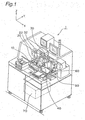
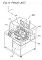
- Fig. 12 shows a conventional component mounting system.
- the system generally indicated by reference numeral 100 includes a component supply 110 for supplying components; a transport head 120 for picking up one of the components from the component supply 110 and then turning the component upside down to orient the component in a predetermined mounting direction; a placement head 130 for receiving the component from the transport head 120 and then placing the component onto the substrate or printed circuit board in place; an imaging camera 140 for capturing an image of the component received by the placement head 130; a holder 150 for holding and then positioning the circuit board in place in the system 100; another imaging camera 160 for capturing an indication marked on the circuit board; a controller 170 for controlling the whole operation of the system 100.
- the placement head 130 which is supported to move horizontally in the X-direction in Fig. 12, is equipped with a vacuum nozzle or quill capable of rotating about a vertical Z-axis.
- the component supply 110 is provided with a number of components 111 supported and separated from another on an expanded plate 112.
- the components 111 are each recognized by an imaging device or camera 113.
- the controller 170 moves the component supply 110 so that one component 111a to be mounted in the subsequent mounting is positioned in a predetermined pickup position.
- the transport head 120 travels to a position right above the component 111a, moves downward to contact the component 111a, and then sucks the component 111a for unloading. After unloading, the transport head 120 moves upward and then travels in the X-direction to a transfer station.
- the transport head 120 together with the component turns upside down as indicated by arrow 121.
- the placement head 130 approaches the component 111a in the upright position from above to receive the component from the transport head 120. Then, the placement head 130 moves upward and then travels in the X-direction toward a placement station.
- the transport head 120 after being deprived of the component, moves back to the pickup station for the subsequent pickup operation
- a circuit board 151 is transported to and then held in position by the holder 150.
- the imaging device or camera 160 approaches the circuit board 151 to capture the indication defined on the circuit board, indicative of a reference position for the mounting of the component.
- the captured image is then transmitted to the controller 170.
- the imaging device 160 together with another imaging device 140 is mounted on an optical head 180.
- the optical head 180 moves back in the X-direction toward the placement head 130 that is running in the opposite direction.
- the placement head 130 comes to a halt.
- the component 111a held by the placement head 130 is recognized by the imaging device 140.
- the image captured by the imaging device 140 is transmitted to the controller 170.
- the sucking nozzle of the placement head 130 for sucking and holding the component 111a is maintained in an elevated position. This prevents the nozzle from making a conflict with the imaging device 140.
- the sucked component 130 is held within a field of the imaging device 140.
- the placement head 130 with the component 111a restarts travelling in the X-direction again toward the mounting station.
- the recognition results of the component 111a and the circuit board 151 are used for calculations performed in the controller 170.
- the controller 170 calculates the displacement in the X-direction of the placement head 130 for the mounting of the component 111a onto the predetermined position of the circuit board 151.
- Also calculated in the controller 70 are the rotational angle of the nozzle about the Z-axis and the displacement of the circuit board 151.
- the placement head 130 travels in the X-direction to a position where it opposes the circuit board 151. At this moment, the corrections for the nozzle and the circuit board 151 have already been completed.
- the placement head 130 causes the nozzle to move downward, so that the component 111a is mounted in position on the circuit board 151.
- the placement head 130 After mounting, the placement head 130 releases the component 111a and then pulls up the nozzle in the Z-direction to a certain level. Then, the imaging head 180 moves in between the circuit board 151 and the placement head 130 so that the imaging device 160 determines whether the component 111a takes the predetermined position on the circuit board 151. Another imaging device 140, on the other hand, recognizes whether the placement head 130, in particular the tip end of the nozzle, carries any debris. Once the recognition has been completed, the placement head 130 moves back in the X-direction for receiving the next component. By the repetition of the series of operations described above, the components on the expanded panel 112 are mounted sequentially on the respective circuit boards with a cycle time of about, for example, 1.9 seconds.
- the conventional component mounting system has several drawbacks in the recognition operations.
- the placement head 130 after it has received the component 111a is accelerated to a certain velocity.
- the placement head 130 comes to a temporal halt for the recognition of the component 111a by the imaging device 160.
- This requires further acceleration and deceleration of the placement head 130 before the actual mounting of the component 111a.
- the placement head 130 after it has come to a halt continues to vibrate for a certain period, which requires the imaging camera 160 to wait until the termination of the vibration in order to attain the precise recognition of the component 111a. This in turn reduces the operational efficiency of the mounting.
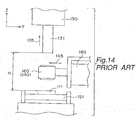
- the nozzle 131 of the placement head 130 is moved upward to the elevated position as indicated by arrow 135. Then, as indicated by arrow 145, the optical head 180 moves in between the elevated nozzle 131 and the circuit board 151 for imaging by the imaging devices 140 and 160.
- a distance between the elevated nozzle and the circuit board, indicated by alphabet H, is designed to be about 40mm, for example, in order to prevent the interference of the optical head 180 with the nozzle 131 and also to ensure a proper imaging operation of the optical head 180.
- the elevation of the nozzle 131 requires 0.1 second even by the use of a high-speed voice coil motor.
- the conventional mounting system is equipped with an interlock to avoid the interference of the optical head 180 with the placement head 130 during the recognition operations by the optical head 180 before and after the mounting. This complicates the structure of the mounting system 100 and makes the system less economical.
- the conventional recognition procedure requires the placement head 130 and the optical head 180 to travel along complicated passes, respectively.
- This in turn requires the mounting system to have a more number of drive shafts and acceleration/deceleration operations, which further reduces the positional precision of the moving part and thereby the imaging quality.
- an object of the present invention is to provide an improved component mounting apparatus and method.
- the component mounting apparatus of the present invention has a component supply provided at a first station for supplying a component; a transport head for picking up the component at the first station from the component supply and then transporting the component to a second station; a placement head for receiving the component from the transport head at the second station and then transporting the component to a third station; a substrate provided at the third station, the substrate being provided with the component from the placement head at the third station; and an imaging unit for recognizing the component held by the placement head; wherein the first imaging unit is positioned in or in the vicinity of the second station.
- Another component mounting apparatus of the present invention has a component supply provided at a first station for supplying a component; a transport head for picking up the component at the first station from the component supply and then transporting the component to a second station; a placement head for receiving the component from the transport head at the second station and then transporting the component to a third station; a substrate holder for holding a substrate, the substrate holder being movable between the third station and a fourth station spaced a certain distance away from the third station; a first imaging unit for recognizing the component held by the placement head; and a second imaging unit positioned at the fourth station for recognizing the substrate.
- Another component mounting apparatus of the present invention has a component supply provided at a first station for supplying a component; a transport head for picking up the component at the first station from the component supply and then transporting the component to a second station; a placement head for receiving the component from the transport head at the second station and then transporting the component to a third station; a substrate holder provided at the third station for holding a substrate, the substrate being provided with the component from the placement head at the third station; a first imaging unit for recognizing the component held by the placement head; and a second imaging unit for recognizing the substrate; wherein the first and second imaging units are arranged not to interfere with a passage of the placement head.
- a component mounting method has picking up a component by a transport head from a component supply at a first station; transporting the component from the first station to a second station by the transport head; transferring the component from the transport head to a placement head at the second station; recognizing the component received by the placement head at or in the vicinity of the second station; transporting the component from the second station to a third station by the placement head; placing the component onto a substrate at the third station by the placement head; and controlling the step of placing the component onto the substrate based upon information obtained by the recognition of the component.
- a vacuum nozzle is used for holding a component and a circuit board is employed for a substrate to which the component is mounted
- the present invention is not limited thereto.
- the vacuum nozzle may be replaced by another mechanical holder or chuck for holding the component by a mechanical engagement with the component.
- the substrate may be another device or housing to which the component is mounted.
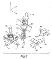
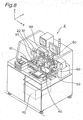
- the system 1 has a component supply 10 for supplying components to the system 1; a transport head 20 for picking up each component from the component supply 10 and then turning upside down to orient the component in a direction along which the component is mounted onto the substrate; a placement head 30 for receiving the component from the transport head 20 and then mounting the component onto the substrate; an imaging device or camera 40 for imaging a position of the component held by the placement head 30 immediately after the component has been transferred to the placement head 30; a substrate holder 50 for holding and then positioning the substrate in place in the system 1; another imaging device or camera 60 for imaging a position of the substrate; and a controller 70 for controlling the whole operation of the system 1.
- a component supply 10 for supplying components to the system 1
- a transport head 20 for picking up each component from the component supply 10 and then turning upside down to orient the component in a direction along which the component is mounted onto the substrate
- a placement head 30 for receiving the component from the transport head 20 and then mounting the component onto the substrate
- an imaging device or camera 40 for imaging a position
- the transport head 20 is supported by a horizontal guide (not shown) extending in the X-direction and is connected with a motor 22 so that by the driving of the motor 22 the head 20 moves back and forth in the X-direction.
- the placement head 30 is also supported by a horizontal guide (not shown) extending in the X-direction and is connected with a motor 32 so that by the driving of the motor 32 the head 30 moves back and forth in the X-direction.
- the imaging cameras 40 and 60 are located in different positions.
- the imaging camera 40 is mounted adjacent a transfer station where the transport head 20 transfers the component to the placement head 30.
- the imaging camera 60 is mounted on the rear side of and outside a region where the placement head 30 travels in the X-direction so that the imaging camera 60 does not interfere with the placement head 30.
- the component supply 10 has an upper table, i.e., X-table (not shown), for supporting the components and a lower table, i.e., Y-table (also not shown), for supporting the X-table.
- the tables are mounted so that the lower table moves back and forth in Y-direction relative to the system and the upper table moves back and forth in X-direction relative to the lower table.
- the tables are drivingly. connected with respective motors 13 and 14, so that by the driving of the motors 13 and 14 the tables move back and forth in X- and Y-directions independently, allowing a designated component to take a predetermined pickup position.
- the transport head 20 is supported by a horizontal guide (not shown) extending in the X-direction and is connected with a motor 22 so that by the driving of the motor the head 20 moves back and forth in the X-direction.
- a motor 21 is mounted on the transport head 20 for turning the picked component upside down, allowing the component to be transported for the placement head 30 in a condition where the connecting portion of the component is faced down.
- the placement head 30 is slidably supported by a horizontal guide (not shown) extending in the X-direction and is connected with a motor 32 so that by the driving of the motor 32 the head 30 moves back and forth in the X-direction.
- a motor 33 is mounted on the placement head 30 for rotating the component about the vertical Z-axis and thereby orienting the component in a predetermined direction.
- Another motor 34 is provided in the placement head 30 for the vertical movement of a component holding part of the placement head 30.
- the substrate holder 50 which is slidably supported by a guide rail (not shown) extending in the Y-direction, includes a motor 52 for its movement in the Y-directions along the guide rail.
- the imaging device 60 which is also slidably supported by a guide rail 60a extending in the X-direction, has a motor 62 for its movement in the X-direction along the guide rail (not shown). As described above, the component imaging device 40 is fixed in the system 1 at a position where it can oppose the placement head 30.
- Fig. 3 shows a positional relationship of various parts and stations (i.e., pickup station A, transfer station B, and mount station C) in the system.
- each component supported on the component supply 10 is picked up by the transport head 20 at the pickup station A.
- the transport head 20 moves in the X-direction (from left to right in the drawing) to the transfer station B where it turns upside down to overturn the component into a state in which the component can be mounted on the substrate from its above.
- the overturned component 11 is then transferred to the placement head 30.
- the placement head 30 with the component 11 moves to the placement station C to mount the component 11 onto the predetermined position of the substrate 51.
- an imaging device or camera 12 is arranged at the pickup station A.
- the imaging devices 40 and 60 are arranged at the transfer and placement stations B and C, respectively.
- the imaging devices 12, 40, and 60 are connected to the controller 70 (see Fig. 1) so that the images captured by the imaging devices are transmitted to the controller 70, respectively.
- the imaging device 60 is positioned on the rear side of the placement head 30 to avoid the interference between the imaging device 60 and the placement head 30.
- FIGs. 4A to 4H operations performed at respective stations will be described in detail hereinafter.
- the drawings illustrate the operations performed at the stations A to C, when viewed in the Y-direction.
- the operations performed at the pickup station A are depicted in Figs. 4A and 4B
- operations at the transfer station B are in Figs. 4C to 4E
- operations at the placement station C are in Figs. 4F to 4H.
- each of the components 11 supported by the component supply 10 is recognized by the imaging device 12 from above.
- the controller 70 moves the component supply 10 so that the component 11 to be picked up and then mounted on the substrate 51 takes the pickup position.
- the transport head 20 reaches above the pickup position and then moves downward to pick up the component at the pickup position.
- the transport head 20 moves upward and then travels toward the transfer station B, i.e., from left to right in the drawing.
- the imaging device 12 is located above the pass of the transport head 20 so that no interference would be made between them.
- the transport head 20 turns upside down so that the component is oriented into a placement condition.
- the electric connections such as solder bumps provided at a bottom surface of the component to be directed downward for the mounting onto the substrate.
- solder bumps are widely used for the electrical connections between the component and wires on the circuit board for the mounting of, for example, an oscillator, the electrical connections can be performed by the use of a conductive adhesive.
- a top surface of the component, typically without any bump, is easy. to be received or sucked by the vacuum nozzle of the placement head 30.
- the turning operation of the transport head 20 is performed at the transfer station B in this embodiment, it can be done as the transport head 20 moves from the pickup station A to the transfer station B.
- the transfer of the component is performed vertically from the transport head 20 to the placement head 30, it can be done in any direction such as horizontally or obliquely.
- the vacuum nozzle of the placement head 30 moves down toward the transport head 20 positioned below the placement head 30 to contact with and then suck the component 11. Simultaneously with this, the transport head 20 releases the component 11, causing the component 11 to be transferred to the placement head 30.
- the transport head 20 moves away from the transfer station B toward the pickup station A (i.e., from right to left in the drawing) for the subsequent pickup operation of the component 11.
- the movement of the transport head 20 away from the transfer station B allows the component 11 held by the placement head 30 to fall within the field of the imaging device 40 located under the transfer station B.
- the imaging device 40 recognizes the component 11 held by the placement head 30.
- The. image of the component is then transmitted to the controller 70 by which the position of the component 11, including X- and Y-lateral positions of its center, angular orientation, is determined.
- the substrate 51 is transported from a substrate supply not shown into the placement station C and then held by the substrate holder 50.
- the substrate 51 is opposed to the imaging device 60 for capturing the image of the substrate to identify respective locations of indications marked on the substrate.
- the substrate 51 as well as the substrate holder 50 is moved from the placement station C to an offset position, spaced rearward away from the station C. Mounted above the offset position is the imaging device 60 for picking up image of the indications.
- the substrate holder 50 together with the substrate 51 is carried back to the placement station C, as shown by the dotted lines in Fig. 4I.
- the imaging device in the conventional system is designed to move in two directions, i.e., X- and Y-directions, which requires two feed mechanisms.
- the imaging device 60 of the present invention moves back and forth only in the X-direction. This means that one of the two feed mechanisms can be eliminated from the system, which is more economical and improves the quality of the recognition.
- the imaging device is designed to move into the operational position in which it opposes the substrate.
- the placement head as well as the vacuum nozzle should be moved up and away from the imaging device. This requires another waiting time for the placement head, which results in the extension of the overall mounting time.
- the placement head 30 occupies a certain region spaced away from that of the imaging device 60, which ensures that no interference would occur between them. This also allows the imaging device 60 to pick up images at any time, irrelevant to the position of the placement head 30, reducing the mounting time.
- the controller 70 determines a positional deviation between a predetermined sucking point and an actual sucking point by the nozzle and an angular orientation of the component, by the use of the image or signals transmitted from the imaging device 40. Also, the controller 70 determines a positional deviation between the predetermined and the actual positions of the indications on the substrate 51, by the use of the image or signals transmitted from the imaging device 60. Taking account of these deviations, the controller 70 calculates a travelling distance to the placement station, a rotating angle of the nozzle 31 about the vertical Z-axis, and a displacement of the substrate 51 with respect to the Y-direction. Based upon the calculation, operations of the motors for moving the placement head 30 and the substrate 51 are controlled by the controller 70.
- the placement head 30 After the transfer and the recognition of the component at the transfer station B, the placement head 30 begins to move toward the placement station C (i.e., from left to right in the drawing). Also, after the correction of the positional deviation and the angular orientation by the controller 70, the placement head 30 moves to the placement station C, as shown in Fig. 4G. Thereafter, as shown in Fig. 4H the placement head 30 places the component 11 in place on the substrate 51.
- the nozzle 31 sucking and holding the component moves down with the placement head 30 toward the substrate 51.
- the placement head 30 forces the component 11 against the substrate 51.
- the placement head 30 applies a high frequency vibration to the component 11, causing the solder bumps to be connected with the substrate.
- the vibration may be an ultrasonic wave generated by a piezoelectric device.
- the ultrasonic wave has an amplitude of about 1 micron and a frequency of about 63,000 per minute.
- the imaging device 40 picks up the image of the placement head 30 as the head is waiting for the next transfer operation to determine the existence of debris. If the debris is detected, the system suspends the subsequent operations for the removal of the debris, which would otherwise cause any damage to the component 11 or the nozzle 31. This operation can equally be applied to the transport head 20. In this instance, the imaging device 40 picks up the image of the nozzle of the transport head 20 to detect any debris on the nozzle. Preferably, this is performed as the placement head 30 is moving toward the placement station C.
- the substrate 51 may move rearward to a shifted position where it opposes the imaging device.60 for picking up an image of the substrate 51 and thereby determining whether the component 11 has been mounted in place on the substrate 51.
- the imaging device 40 positioned at the transfer station B allows the component 11 to be recognized before the placement head 30 begins to move toward the placement station C, which ensures the placement head 30 to move continuously without any halt.
- the position of the imaging device 40 is not limited thereto.
- the imaging device 40 may be positioned in the vicinity of the transfer station B or in another position spaced slightly away from the position where the component is transferred from the transport head 20 to the placement head 30.
- the reason why the imaging device 40 is placed at or immediately adjacent the transfer station is to avoid any loss of time which is caused in the conventional operation that requires the placement head needs to halt after it has reached the maximum speed in the course of moving from the transfer station to the placement station for the recognition of the component and also the imaging device to wait until the vibration caused by the halt will come to an end.
- the time loss can be reduced to some extent even when the placement head makes a halt before it reaches the maximum speed. Therefore, the terms “vicinity” and “spaced slightly” means a certain range in which the placement head is accelerated up to the maximum speed.
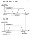
- Figs. 5A and 5B descriptions will be made to this in details.
- a certain time of about 0.1 second is required for damping the vibration of the placement head caused by the inertial force of the placement head with a weight of about 10 kilograms, for example.
- the placement head moves to the placement station, during which it is accelerated and then decelerated again.
- the transport head 20 moves away from the field of the imaging device. Immediately after that, the component held by the placement head 30 is recognized. Then, the placement head 30 accelerates to the maximum speed, moves with the speed, and then decelerates to reach the placement station. This eliminates the additional acceleration and deceleration required in the conventional system, which decreases the cycle time by about 0.2 seconds.
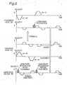
- Fig. 6 shows a relationship of movements and operations for the placement head 30, transport head 20, and substrate holder 50
- the placement head 30 moves back from the placement station C to the transfer station B.
- the transport head 20 which has already picked up the subsequent component moves from the pickup station A toward the transfer station B.
- the heads 20 and 30 halt to oppose each other at the transfer station B and then approach each other for the transfer of the component from the transport head to the placement head, which is illustrated by a hollow arrow directed upward.
- the transport head moves back toward the pickup station, allowing the recognition of the component held on the placement head 30 by the use of the imaging device.
- the recognition operation of the component is illustrated as a hatched box.
- the placement head 30 moves toward the placement station C.
- the recognition operation for the substrate 51 is performed, which is illustrated as another hatched box.
- the substrate holder 50 moves to the placement station C where the placement head 30 places the component on the substrate 51, which is illustrated by a hollow arrow directed downward.
- the transport head 20 picks up the subsequent component from the component supply. The above-described operations are repeated for each component.
- the fixed imaging device 40 does not need X- and Y-feed mechanisms needed for the conventional system. This not only simplifies the structure of the system but also increases the positioning and imaging precision. Meanwhile, the imaging device 40 may be designed to move Y- or Z-direction, which will be described below. Even in this embodiment, one of the two mechanisms is eliminated. This is illustrated in the table by bracketing.
- X-feed For the imaging device 60, only one (i.e., X-feed) mechanism is needed. This means that one mechanism can be eliminated from the conventional system which needs two (X- and Y-) feed mechanisms. This is because the substrate 51 is shifted away from the placement station to another position for its recognition by the imaging device 60. The reduction of the feed mechanism also increases the recognition precision of the substrate. Although the system is designed so that the substrate holder moves back and forth in Y-direction, it may be moved in another direction provided that the substrate can be recognized by the imaging device in a certain position away from the placement station and the imaging device 60 does not make any conflict with the placement head 30.
- the system of the present invention can shorten the moving passes of respective moving elements.
- the vacuum nozzle 31 of the placement head 30 is required to move about 40mm in the vertical direction in order to avoid the interference with the imaging devices.
- the imaging devices 40 and 60 are located at difference positions and outside the passage of the placement head 30 in the movements in the X-direction. This minimizes the vertical movements of the nozzle 31 in the placement head 30 at the transfer and placement stations down to about 1mm, for example, which is required for the prevention of the interference with the component.
- the imaging device for the substrate recognition is assembled with another imaging device for the component recognition.
- the substrate recognition device is separated from the other component recognition device so that it is served only for the recognition of the substrate. Therefore, the substrate recognition device is required to move only a limited distance of about 10mm, for example, which might differ depending upon the size or the purpose of the component.
- the reduction of the moving distance results in the reduction of the inertial force of the movement mechanism as well as the necessary rigidity of the supporting structure and also in the increase of the precision of the positioning.
- the system 1 of the present invention has a number of moving parts.
- the placement head 30 moves about 500mm in the X-direction between the transfer and placement stations B and C.
- the movement of each element should be controlled precisely in order to attain the precise alignment of the components on the substrate.
- the system employs servomotors, pulse-motors, and/or voice-coil motors for controlling the moving distance of the elements.
- a linear scale may be used for each moving mechanism in order to attain a more precise control of the moving distance.
- the linear scale which is a pulse encoder for measuring a liner displacement, has a reference scale with indices marked optically or magnetically and a detector mounted for movement on and relative to the reference scale, which ensures a precise movement control. Taking such feature into account, the linear scale is preferably used for the compensation of the change of moving distance that might be caused by heat.
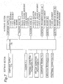
- Fig. 7 is a circuit diagram showing various parts incorporated in respective devices described above.
- the system has a hardware section and a software section.
- the hardware section includes the component supply 10, transport head 20, placement head 30, component recognition device 40, substrate holder 50, and substrate recognition device 60.
- the software section includes various processing units for controlling necessary operations for supplying component, sucking component, calculating an amount for position correction, calculating an amount for angular correction, recognizing component, recognizing reference-indication, and correcting position.
- the hardware and software elements are integrated with the controller that controls the overall operations of the elements.
- Each of the hardware elements whose operations are already described above has various drivers connected through respective lines extending out from the elements.
- the controller receives signals from respective units of the software section and, based on which, controls respective drivers.
- the component supply processing unit controls the movement of the component supply 10 so that the component to be picked up is placed at the pickup position.
- the component sucking processing unit controls timing and vacuum for the component sucking by nozzles mounted on the transfer and placement heads.
- the units for calculating positional and angular corrections calculates, from signals transmitted from the recognition device 40, a moving distance of the placement head 30 in the X-direction for the mounting and the amount of angular correction for the nozzle 31 about the vertical Z-axis.
- the component recognition unit controls the recognition timing by the recognition device 40 and the field of the device.
- the reference-indication recognition unit controls the recognition timing and the field of the substrate recognition device 60 and, based upon the recognition by the device 60, the position correction unit controls the moving distance of substrate holder 50 in the Y-direction.
- the recognition devices 40 and 60 are separated from each other, which allows respective devices 40 and 60 to be controlled independently, without any restriction imposed by the other device.
- FIG. 8 another mounting system and method according to the second embodiment of the present invention will be described hereinafter.
- the component mounting system of this embodiment is similar to that of the first embodiment except that the system 2 has a second placement head 80. Therefore, like parts bears like reference numerals throughout the drawings.
- the placement head 30 receives the component at the transfer station B and then moves to the placement station C for the mounting of the component.
- the mounting of the component at the placement station C is completed by the ultrasonic connection, which needs a relatively extended period of time of about 0.5 seconds. This increases a waiting time of associated element or elements, which results in an unwanted extension of the overall time for mounting.
- the first and second placement heads bear respective functions and thereby enhance the productivity of the mounting.
- the system 2 is designed so that the placement head 30 serves for a first step of mounting in which the component 11 is mounted on the substrate 51 and then connected temporally by the ultrasonic vibration.
- the temporal connection requires only a limited time of about 0.1 second.
- the placement head 30 moves back from the placement station C to the transfer station B where it receives the next component from the transport head.
- the second placement head 80 serves for a second step of mounting in which it applies the ultrasonic vibration again to the temporally connected component 11 for the permanent connection of the component to the substrate.
- the permanent connection requires another time of about 0.4 seconds.
- the first (temporal) and second (permanent) connections by the placement heads 30 and 80 require about 0.1 and 0.4 seconds, respectively. Therefore, the total connection time appears to be identical to that required by the system 1 of the first embodiment.
- the placement head 30 can proceed to receive the next component, which means that the overall time for mounting per component is substantially reduced by, for example, 0.4 seconds.
- the functional separation using two placement heads causes the overall time for mounting of the component to be reduced considerably and also the productivity of the system to be increased significantly.
- the two-step connection provides a drastic increase of the connecting force of the component than the one-step connection.
- bracket or box cover In order to provide the ultrasonic vibration to the component effectively, another holder in the form of bracket or box cover may be used for holding the component and then forcing it to the substrate.
- the position and/or orientation of component mounted temporally on the substrate may be recognized by the recognition device and, if necessary, corrected at the permanent connection base upon the recognition result.
- the substrate 51 is transported rearward to oppose the fixed recognition device 60 for the recognition of the component mounted temporally on the substrate. Then, based on the positional information transmitted from the recognition device 60, the controller 70 calculates the amount for X-, Y-, and/or angular correction and then controls the movement of the other placement head 80.
- the recognition device 40 recognizes the component holding portion of the placement head 30 immediately after the temporal mounting of the component and the component holding portion of another placement head 80 before the permanent mounting of the component. This allows the controller 70 to prevent any possible accidents, which may be caused by the existence of debris at the component holding portions of the placement heads. Also, this allows the placement head 80 to hold the temporally mounted component positively.
- Figs. 9A to 9J schematically shows a series of operations performed at the pickup, transfer, and placement stations by the system 2. As can be seen from the drawings, the operations illustrated in Figs. 9A to 9G are the same as those illustrated in and described with reference to Figs. 4A to 4G.
- the component 11 is temporally mounted on and connected with the substrate 51 as shown in Fig. 9H.
- the placement head 30 moves back in the X-direction to the transfer station B for the transfer operation of the next component.
- the substrate 51 moves rearward in the Y-direction to oppose the recognition device 60.
- the recognition device 60 recognizes the component temporally connected on the substrate 51 and then transmits the recognized image signal to the controller 70.
- the positional relationship between the substrate 51 and the recognition device 60 is similar to that shown in Fig. 9K.
- the substrate 51 moves back in the Y-direction to the placement station where it opposes the second placement head 80.
- the placement head 80 moves downward to hold the temporally connected component 11. Also, the placement head 80 forces the component 11 to the substrate and then provides the component with the ultrasonic vibration for the permanent connection of the component to the substrate.
- the component holding portion of the placement head 80 is defined in the form of bracket.
- the placement head takes another configuration suitable for the positioning of the component and the application of the ultrasonic vibrations to the component.
- the controller 70 suspends the mounting operation to make a warning. In this case, if necessary, the substrate 51 may be discarded automatically or manually.
- FIGs. 10A and 10B illustrate positional relationships between the component sucked and held by the nozzle 31 of the placement head 30 and the recognition devices in the conventional system (Fig. 10A) and the system of the present invention (Fig. 10B), respectively.
- the space between the component 111a held by the nozzle 131 of the placement head 130 and the substance 151 is so limited. This fails to ensure a distance, between the recognition device 140 and the component, necessary for the proper recognition of the component, which reduces the resolution of the image of, in particular, the large size component. Contrary to this, the recognition device 40 is mounted only for the recognition of the component and therefore fixed in the system, which does not need additional space to avoid the interference with the neighboring members. This in turn defines a larger space between the recognition device 40 and the component than the conventional system, which increases the field and/or resolution of the recognition device 40. The increase of the field and resolution are illustrated by dotted lines ⁇ and long and short dotted lines ⁇ in Fig. 10B
- the recognition device 40 is designed to shift in the direction indicated by arrow 45, i.e., the X- or Y-direction, to a certain extent. With the arrangement, first the recognition device 40 occupies a first position where it recognizes a part of the component. Then, the recognition device 40 moves to a second position where it recognizes the remaining part of the component. Partial images of the component are then combined and processed at the controller for the subsequent processes such as position and/or angular correction of the component.
- This process allows the recognition device to capture the entire image of the component with a necessary resolution even within a limited space. This in turn means that the moving range of the recognition device for the component recognition can be minimized. In addition, the horizontal movement of the recognition device 40 may reduce the likelihood that it suffers from any damage by the possible drop of the component or other members.
- the recognition device 40 is designed to move vertically, i.e., in the Z-direction between a lowered position indicated by solid lines and an elevated position indicated by dotted lines.
- This embodiment allows the recognition device 40 to shift its focus vertically so that the components with different heights or at different levels can be recognized without any defocus.
- the larger component 11 is moved down from the elevated to the lowered position to extend its field, so that the entire image of the larger component can be captured by one shot.
- the recognition device 40 due to its movability in the vertical direction, is also available for the detection of debris carried by the component holding portion of the transfer and placement heads 20 and 30.
- the recognition device 40 is supported by a horizontal axis not shown so that it rotates as indicated by arrow 47.
- This arrangement allows the recognition device 40 to take between a first position (indicated by solid lines) where it recognizes a part of the component and a second position (indicated by dotted lines) where it recognizes the remaining part of the component.
- the recognition device is connected with a driving source such as pulse motor that is controlled by the controller.
- the system may be designed so that the recognition device takes three positions where the recognition device captures respective parts of the component.
- the recognition unit has two fixed recognition devices 40a and 40b in order to enlarge the field of the recognition unit.
- This arrangement allows the larger component to be recognized by two recognition devices with a high resolution. Also, this arrangement may be used so that either one of the recognition devices works for a small component, and both for a large component.
- the number of the recognition is not limited to two.
- the recognition device 40 is oriented horizontally.
- the recognition unit has a mirror 41.
- the mirror 41 is located in front of the recognition device 40 and supported for rotation so that the field of the recognition device is reflected and then moved across the component. With this arrangement, the mirror rotates between a first position where the reflected field of the recognition device covers a part of the component and a second position where the reflected field covers the remaining part of the component.
- the mirror is drivingly connected to a motor, such as pulse motor, so that the controller controls the motor to rotate the mirror.
- the mirror may be any member capable of changing a light pass, such as prism.
- the recognition unit has an optical member 42 such as lens positioned between the recognition device 40 and the component 11, allowing the recognition device 40 to pick up the image of larger component.
- the optical member 42 may be supported to move out of the space between the recognition device 40 and the component 11. Two or more optical members may be prepared so that a suitable one of which is selected depending upon the size of the component and/or the required resolution. Also, the optical member 42 may be used in combination with other optical elements such as mirror and prism. Further, the recognition device 40 may be supported for movement not only in this embodiment but also in the previous embodiment in Fig. 11E, which enlarges the field of the recognition device while keeping the required resolution.
Landscapes
- Engineering & Computer Science (AREA)
- Manufacturing & Machinery (AREA)
- Microelectronics & Electronic Packaging (AREA)
- Computer Hardware Design (AREA)
- Power Engineering (AREA)
- Operations Research (AREA)
- Physics & Mathematics (AREA)
- Condensed Matter Physics & Semiconductors (AREA)
- General Physics & Mathematics (AREA)
- Supply And Installment Of Electrical Components (AREA)
- Wire Bonding (AREA)
Applications Claiming Priority (3)
| Application Number | Priority Date | Filing Date | Title |
|---|---|---|---|
| JP2000082263A JP4480840B2 (ja) | 2000-03-23 | 2000-03-23 | 部品実装装置、及び部品実装方法 |
| JP2000082263 | 2000-03-23 | ||
| EP01914193A EP1269812B1 (fr) | 2000-03-23 | 2001-03-23 | Appareil et procede de montage d'un composant |
Related Parent Applications (2)
| Application Number | Title | Priority Date | Filing Date |
|---|---|---|---|
| EP01914193.6 Division | 2001-03-23 | ||
| EP01914193A Division EP1269812B1 (fr) | 2000-03-23 | 2001-03-23 | Appareil et procede de montage d'un composant |
Publications (3)
| Publication Number | Publication Date |
|---|---|
| EP1553815A2 true EP1553815A2 (fr) | 2005-07-13 |
| EP1553815A3 EP1553815A3 (fr) | 2007-11-21 |
| EP1553815B1 EP1553815B1 (fr) | 2010-11-24 |
Family
ID=18599093
Family Applications (2)
| Application Number | Title | Priority Date | Filing Date |
|---|---|---|---|
| EP01914193A Expired - Lifetime EP1269812B1 (fr) | 2000-03-23 | 2001-03-23 | Appareil et procede de montage d'un composant |
| EP05003553A Expired - Lifetime EP1553815B1 (fr) | 2000-03-23 | 2001-03-23 | Appareil et procédé de montage d'un composant |
Family Applications Before (1)
| Application Number | Title | Priority Date | Filing Date |
|---|---|---|---|
| EP01914193A Expired - Lifetime EP1269812B1 (fr) | 2000-03-23 | 2001-03-23 | Appareil et procede de montage d'un composant |
Country Status (6)
| Country | Link |
|---|---|
| US (2) | US7020953B2 (fr) |
| EP (2) | EP1269812B1 (fr) |
| JP (1) | JP4480840B2 (fr) |
| DE (2) | DE60143548D1 (fr) |
| SG (1) | SG144725A1 (fr) |
| WO (1) | WO2001072097A2 (fr) |
Cited By (1)
| Publication number | Priority date | Publication date | Assignee | Title |
|---|---|---|---|---|
| US8201329B2 (en) | 2006-02-03 | 2012-06-19 | Semiconductor Energy Laboratory Co., Ltd. | Apparatus and method for manufacturing semiconductor device |
Families Citing this family (43)
| Publication number | Priority date | Publication date | Assignee | Title |
|---|---|---|---|---|
| JP2003060395A (ja) * | 2001-08-10 | 2003-02-28 | Matsushita Electric Ind Co Ltd | 電子部品の実装方法および実装装置 |
| US20030086089A1 (en) * | 2001-11-02 | 2003-05-08 | Mike Carlomagno | System and method for rapid alignment and accurate placement of electronic components on a printed circuit board |
| US7716822B2 (en) * | 2002-11-08 | 2010-05-18 | Assembleon N.V. | Method of moving at least two elements of a placement machine |
| TW200419640A (en) * | 2003-02-25 | 2004-10-01 | Matsushita Electric Ind Co Ltd | Electronic component placement machine and electronic component placement method |
| US7754832B2 (en) * | 2003-02-28 | 2010-07-13 | The Regents Of The University Of California | Block copolyolefins possessing a tapered structure |
| JP4334892B2 (ja) * | 2003-03-20 | 2009-09-30 | パナソニック株式会社 | 部品実装方法 |
| WO2005020657A1 (fr) * | 2003-08-20 | 2005-03-03 | Murata Manufacturing Co., Ltd. | Dispositif de montage de pieces et procede de montage de pieces |
| JP4390503B2 (ja) | 2003-08-27 | 2009-12-24 | パナソニック株式会社 | 部品実装装置及び部品実装方法 |
| JP4516354B2 (ja) * | 2004-05-17 | 2010-08-04 | パナソニック株式会社 | 部品供給方法 |
| EP1694107A1 (fr) * | 2005-02-17 | 2006-08-23 | KLARER, Christoph | Appareil et méthode pour la prise et le transfert d'un composant électronique |
| JP4555118B2 (ja) * | 2005-02-22 | 2010-09-29 | パナソニック株式会社 | 部品装着装置及び部品保持部材の判別方法 |
| JP2006268090A (ja) * | 2005-03-22 | 2006-10-05 | Fujitsu Ltd | Rfidタグ |
| JP4912900B2 (ja) * | 2006-02-03 | 2012-04-11 | 株式会社半導体エネルギー研究所 | 半導体装置の作製方法 |
| NL1032810C2 (nl) * | 2006-11-03 | 2008-05-06 | Assembleon Bv | Werkwijze voor het plaatsen van een component op een substraat alsmede een dergelijke inrichting. |
| JP4765942B2 (ja) * | 2007-01-10 | 2011-09-07 | 株式会社デンソー | 監視装置と監視方法、および制御装置と制御方法 |
| CH698718B1 (de) * | 2007-01-31 | 2009-10-15 | Oerlikon Assembly Equipment Ag | Vorrichtung für die Montage eines Flipchips auf einem Substrat. |
| SG147353A1 (en) * | 2007-05-07 | 2008-11-28 | Mfg Integration Technology Ltd | Apparatus for object processing |
| JP2009111312A (ja) * | 2007-11-01 | 2009-05-21 | Trinc:Kk | チップマウンター |
| TW200931543A (en) * | 2007-12-03 | 2009-07-16 | Panasonic Corp | Chip mounting system |
| CN101600336A (zh) * | 2008-06-04 | 2009-12-09 | 鸿富锦精密工业(深圳)有限公司 | 散热器安装治具 |
| KR20100033200A (ko) * | 2008-09-19 | 2010-03-29 | 삼성전자주식회사 | 반도체 패키지 제조 장치 및 방법 |
| JP4788759B2 (ja) * | 2008-11-20 | 2011-10-05 | パナソニック株式会社 | 部品実装装置 |
| US20110182701A1 (en) * | 2010-01-28 | 2011-07-28 | Ui Holding Co. | Method and apparatus for transferring die from a wafer |
| KR101710631B1 (ko) * | 2010-12-23 | 2017-03-08 | 삼성전자주식회사 | 손 떨림 보정 모듈을 구비하는 디지털 영상 촬영 장치 및 이의 제어 방법 |
| KR20120096727A (ko) * | 2011-02-23 | 2012-08-31 | 삼성테크윈 주식회사 | 베어 다이를 픽업 및 실장하기 위한 장치 및 방법 |
| JP5691001B2 (ja) * | 2011-11-08 | 2015-04-01 | パナソニックIpマネジメント株式会社 | 反転ヘッド |
| JP5746610B2 (ja) * | 2011-12-22 | 2015-07-08 | ヤマハ発動機株式会社 | 部品撮像装置および同装置を備えた部品実装装置 |
| CN104770075B (zh) * | 2012-10-29 | 2017-12-26 | 富士机械制造株式会社 | 元件供给装置 |
| US9036354B2 (en) * | 2013-01-15 | 2015-05-19 | Flextronics, Ap, Llc | Heat sink thermal press for phase change heat sink material |
| US9015928B2 (en) * | 2013-07-25 | 2015-04-28 | Panasonic Intellectual Property Management Co., Ltd. | Electronic component mounting apparatus |
| US10568248B2 (en) * | 2013-10-11 | 2020-02-18 | Fuji Corporation | Suction nozzle and component mounting machine |
| JP6115617B2 (ja) * | 2015-11-16 | 2017-04-19 | Tdk株式会社 | 実装装置 |
| CN109314069B (zh) * | 2016-05-13 | 2022-08-12 | Asml荷兰有限公司 | 用于部件堆叠和/或拾放过程的微型多拾取元件 |
| KR102443290B1 (ko) | 2016-07-13 | 2022-09-14 | 유니버셜 인스트루먼츠 코퍼레이션 | 모듈식 다이 핸들링 시스템 |
| CN106228913B (zh) * | 2016-08-24 | 2022-12-30 | 京东方科技集团股份有限公司 | 转印设备及其转印方法 |
| CN107366849B (zh) * | 2017-08-08 | 2019-06-11 | 浙江美科电器有限公司 | 灯条生产设备 |
| CN107514555B (zh) * | 2017-08-08 | 2020-06-19 | 浙江美科电器有限公司 | Led灯条制造装置 |
| CN107543059B (zh) * | 2017-08-08 | 2019-04-12 | 浙江美科电器有限公司 | 高效率灯带生产装置 |
| CN109773474B (zh) | 2017-11-13 | 2021-07-13 | 宁波舜宇光电信息有限公司 | 光学组件的组装设备及组装方法 |
| US20220059406A1 (en) * | 2020-08-21 | 2022-02-24 | Advanced Semiconductor Engineering, Inc. | Method for manufacturing semiconductor package |
| CN112261865B (zh) * | 2020-10-13 | 2023-06-20 | 常州铭赛机器人科技股份有限公司 | 表面贴装设备及表面贴装方法 |
| CN114521103B (zh) * | 2022-03-26 | 2024-01-26 | 宁波诚兴道电子科技有限公司 | 一种pcba线路板自动贴片设备及工艺 |
| CN114828445B (zh) * | 2022-05-24 | 2023-09-15 | 苏州创阈星智能科技有限公司 | 一种安装设备 |
Citations (2)
| Publication number | Priority date | Publication date | Assignee | Title |
|---|---|---|---|---|
| US5342460A (en) * | 1989-06-13 | 1994-08-30 | Matsushita Electric Industrial Co., Ltd. | Outer lead bonding apparatus |
| WO1999043192A1 (fr) * | 1998-02-17 | 1999-08-26 | Datacon Semiconductor Equipment Gmbh | Dispositif pour positionner des circuits electroniques places sur une feuille |
Family Cites Families (13)
| Publication number | Priority date | Publication date | Assignee | Title |
|---|---|---|---|---|
| DE3532500C2 (de) * | 1984-09-17 | 1996-03-14 | Tdk Corp | Pneumatisch betätigter Bestückungskopf mit Saugkammer für eine Saugpipette |
| JPH0760841B2 (ja) | 1988-08-22 | 1995-06-28 | 松下電器産業株式会社 | 電子部品実装装置 |
| US5040291A (en) * | 1990-05-04 | 1991-08-20 | Universal Instruments Corporation | Multi-spindle pick and place method and apparatus |
| JP3159266B2 (ja) * | 1991-02-14 | 2001-04-23 | 三洋電機株式会社 | 作業装置 |
| EP0578136B1 (fr) * | 1992-07-01 | 1995-11-22 | Yamaha Hatsudoki Kabushiki Kaisha | Procédé de montage de composants et appareil pour cela |
| JPH07153784A (ja) | 1993-11-29 | 1995-06-16 | Sony Corp | ベアチップのプリント基板への実装方法及びフリップチップボンダー |
| JPH07193397A (ja) * | 1993-12-27 | 1995-07-28 | Yamaha Motor Co Ltd | 実装機の吸着ポイント補正装置 |
| JPH08162797A (ja) * | 1994-12-08 | 1996-06-21 | Matsushita Electric Ind Co Ltd | 電子部品実装装置 |
| JP3132353B2 (ja) * | 1995-08-24 | 2001-02-05 | 松下電器産業株式会社 | チップの搭載装置および搭載方法 |
| JP3402876B2 (ja) * | 1995-10-04 | 2003-05-06 | ヤマハ発動機株式会社 | 表面実装機 |
| JP3196626B2 (ja) * | 1995-12-26 | 2001-08-06 | ソニー株式会社 | 部品実装方法 |
| DE69724894T2 (de) * | 1996-03-27 | 2004-07-08 | Assembleon N.V. | Bestückungsverfahren von bauelementen auf einem substrat und bestückautomat dafür |
| JP2001060795A (ja) * | 1999-08-20 | 2001-03-06 | Matsushita Electric Ind Co Ltd | 電子部品実装装置 |
-
2000
- 2000-03-23 JP JP2000082263A patent/JP4480840B2/ja not_active Expired - Lifetime
-
2001
- 2001-03-23 WO PCT/JP2001/002308 patent/WO2001072097A2/fr active IP Right Grant
- 2001-03-23 DE DE60143548T patent/DE60143548D1/de not_active Expired - Lifetime
- 2001-03-23 SG SG200405891-3A patent/SG144725A1/en unknown
- 2001-03-23 EP EP01914193A patent/EP1269812B1/fr not_active Expired - Lifetime
- 2001-03-23 US US10/239,060 patent/US7020953B2/en not_active Expired - Fee Related
- 2001-03-23 DE DE60112416T patent/DE60112416T2/de not_active Expired - Lifetime
- 2001-03-23 EP EP05003553A patent/EP1553815B1/fr not_active Expired - Lifetime
-
2005
- 2005-09-01 US US11/216,074 patent/US7827677B2/en not_active Expired - Fee Related
Patent Citations (2)
| Publication number | Priority date | Publication date | Assignee | Title |
|---|---|---|---|---|
| US5342460A (en) * | 1989-06-13 | 1994-08-30 | Matsushita Electric Industrial Co., Ltd. | Outer lead bonding apparatus |
| WO1999043192A1 (fr) * | 1998-02-17 | 1999-08-26 | Datacon Semiconductor Equipment Gmbh | Dispositif pour positionner des circuits electroniques places sur une feuille |
Cited By (1)
| Publication number | Priority date | Publication date | Assignee | Title |
|---|---|---|---|---|
| US8201329B2 (en) | 2006-02-03 | 2012-06-19 | Semiconductor Energy Laboratory Co., Ltd. | Apparatus and method for manufacturing semiconductor device |
Also Published As
| Publication number | Publication date |
|---|---|
| WO2001072097A2 (fr) | 2001-09-27 |
| EP1553815B1 (fr) | 2010-11-24 |
| WO2001072097A3 (fr) | 2002-06-06 |
| EP1553815A3 (fr) | 2007-11-21 |
| DE60112416T2 (de) | 2006-06-01 |
| US7827677B2 (en) | 2010-11-09 |
| US7020953B2 (en) | 2006-04-04 |
| DE60143548D1 (de) | 2011-01-05 |
| DE60112416D1 (de) | 2005-09-08 |
| JP2001274596A (ja) | 2001-10-05 |
| EP1269812B1 (fr) | 2005-08-03 |
| JP4480840B2 (ja) | 2010-06-16 |
| US20050283972A1 (en) | 2005-12-29 |
| US20040020043A1 (en) | 2004-02-05 |
| EP1269812A2 (fr) | 2003-01-02 |
| SG144725A1 (en) | 2008-08-28 |
Similar Documents
| Publication | Publication Date | Title |
|---|---|---|
| EP1553815B1 (fr) | Appareil et procédé de montage d'un composant | |
| US5249356A (en) | Method and apparatus for mounting electronic component | |
| EP1189497A2 (fr) | Machine et procédé pour le montage de composants sur un substrat | |
| WO2004077910A1 (fr) | Machine de positionnement de composants electroniques et procede pour placer des composants electroniques | |
| US6918176B2 (en) | Mounting apparatus of electronic parts and mounting methods of the same | |
| KR20090092299A (ko) | 부품 인식 장치, 표면 실장기, 및 부품 시험 장치 | |
| JP3879679B2 (ja) | 電子部品搭載装置および電子部品搭載方法 | |
| EP0808090A1 (fr) | Dispositif de réglage de machine de montage de composants électroniques et sa méthode de réglage | |
| JP2004521514A (ja) | 基板に構成部品を実装するための装置 | |
| JP2001127500A (ja) | チップマウンタの部品撮像装置 | |
| JP3738747B2 (ja) | 部品装着装置 | |
| JP2000103031A (ja) | ウェハ用半田印刷装置 | |
| JPH07176896A (ja) | 電子部品実装装置 | |
| JPH09246794A (ja) | 電子部品実装装置および電子部品実装装置におけるノズルの位置検出方法 | |
| JP4296826B2 (ja) | 電子部品搭載装置および電子部品搭載方法 | |
| JP3397127B2 (ja) | 電子部品の実装装置および実装方法 | |
| JPH06155706A (ja) | スクリーン印刷機 | |
| JP2534410B2 (ja) | 部品装着装置 | |
| JPH04179200A (ja) | 部品装着装置 | |
| JP2000312100A (ja) | 表面実装機の部品認識装置 | |
| JPH08255996A (ja) | チップマウンタ | |
| JP2000114785A (ja) | 電子部品装着方法及び電子部品装着装置 | |
| JPH0515499U (ja) | 電子部品搭載装置 | |
| JPH08148897A (ja) | 部品搭載装置 | |
| JPH10303598A (ja) | 部品装着装置 |
Legal Events
| Date | Code | Title | Description |
|---|---|---|---|
| PUAI | Public reference made under article 153(3) epc to a published international application that has entered the european phase |
Free format text: ORIGINAL CODE: 0009012 |
|
| AC | Divisional application: reference to earlier application |
Ref document number: 1269812 Country of ref document: EP Kind code of ref document: P |
|
| AK | Designated contracting states |
Kind code of ref document: A2 Designated state(s): DE GB |
|
| RIN1 | Information on inventor provided before grant (corrected) |
Inventor name: ONOBORI, SHUNJI Inventor name: MINAMITANI, SHOZO Inventor name: KANAYAMA, SHINJI Inventor name: SIDA, SATOSHI Inventor name: SHIMIZU, TAKASHI Inventor name: UENO, YASUHARU |
|
| PUAL | Search report despatched |
Free format text: ORIGINAL CODE: 0009013 |
|
| AK | Designated contracting states |
Kind code of ref document: A3 Designated state(s): DE GB |
|
| 17P | Request for examination filed |
Effective date: 20080521 |
|
| AKX | Designation fees paid |
Designated state(s): DE |
|
| RAP1 | Party data changed (applicant data changed or rights of an application transferred) |
Owner name: PANASONIC CORPORATION |
|
| 17Q | First examination report despatched |
Effective date: 20091216 |
|
| GRAP | Despatch of communication of intention to grant a patent |
Free format text: ORIGINAL CODE: EPIDOSNIGR1 |
|
| GRAS | Grant fee paid |
Free format text: ORIGINAL CODE: EPIDOSNIGR3 |
|
| GRAA | (expected) grant |
Free format text: ORIGINAL CODE: 0009210 |
|
| RIN1 | Information on inventor provided before grant (corrected) |
Inventor name: UENO, YASUHARU Inventor name: ONOBORI, SHUNJI Inventor name: SIDA, SATOSHI Inventor name: SHIMIZU, TAKASHI Inventor name: KANAYAMA, SHINJI Inventor name: MINAMITANI, SHOZO |
|
| AC | Divisional application: reference to earlier application |
Ref document number: 1269812 Country of ref document: EP Kind code of ref document: P |
|
| AK | Designated contracting states |
Kind code of ref document: B1 Designated state(s): DE |
|
| REF | Corresponds to: |
Ref document number: 60143548 Country of ref document: DE Date of ref document: 20110105 Kind code of ref document: P |
|
| PLBE | No opposition filed within time limit |
Free format text: ORIGINAL CODE: 0009261 |
|
| STAA | Information on the status of an ep patent application or granted ep patent |
Free format text: STATUS: NO OPPOSITION FILED WITHIN TIME LIMIT |
|
| 26N | No opposition filed |
Effective date: 20110825 |
|
| REG | Reference to a national code |
Ref country code: DE Ref legal event code: R097 Ref document number: 60143548 Country of ref document: DE Effective date: 20110825 |
|
| PGFP | Annual fee paid to national office [announced via postgrant information from national office to epo] |
Ref country code: DE Payment date: 20120411 Year of fee payment: 12 |
|
| REG | Reference to a national code |
Ref country code: DE Ref legal event code: R119 Ref document number: 60143548 Country of ref document: DE Effective date: 20131001 |
|
| PG25 | Lapsed in a contracting state [announced via postgrant information from national office to epo] |
Ref country code: DE Free format text: LAPSE BECAUSE OF NON-PAYMENT OF DUE FEES Effective date: 20131001 |