EP1553809B1 - Verfahren und gerät zur herstellung eines organischen elektrolumineszenz-displays mit aktiver matrix, organisches elektrolumineszenz-display mit aktiver matrix, herstellungsverfahren für flüssigkristallanordnung, flüssigkristallanordnung, verfahren und gerät zur herstellung von farbfiltersubstrat und farbfiltersubstrat - Google Patents
Verfahren und gerät zur herstellung eines organischen elektrolumineszenz-displays mit aktiver matrix, organisches elektrolumineszenz-display mit aktiver matrix, herstellungsverfahren für flüssigkristallanordnung, flüssigkristallanordnung, verfahren und gerät zur herstellung von farbfiltersubstrat und farbfiltersubstrat Download PDFInfo
- Publication number
- EP1553809B1 EP1553809B1 EP03748557A EP03748557A EP1553809B1 EP 1553809 B1 EP1553809 B1 EP 1553809B1 EP 03748557 A EP03748557 A EP 03748557A EP 03748557 A EP03748557 A EP 03748557A EP 1553809 B1 EP1553809 B1 EP 1553809B1
- Authority
- EP
- European Patent Office
- Prior art keywords
- droplets
- droplet
- nozzle
- color filter
- diameter
- Prior art date
- Legal status (The legal status is an assumption and is not a legal conclusion. Google has not performed a legal analysis and makes no representation as to the accuracy of the status listed.)
- Expired - Lifetime
Links
- 238000000034 method Methods 0.000 title claims abstract description 290
- 238000004519 manufacturing process Methods 0.000 title claims abstract description 94
- 239000011159 matrix material Substances 0.000 title claims abstract description 42
- 239000000758 substrate Substances 0.000 title claims description 283
- 239000004973 liquid crystal related substance Substances 0.000 title claims description 86
- 239000000463 material Substances 0.000 claims abstract description 166
- 239000007788 liquid Substances 0.000 claims abstract description 122
- 125000006850 spacer group Chemical group 0.000 claims description 189
- 230000015572 biosynthetic process Effects 0.000 claims description 90
- 239000003086 colorant Substances 0.000 claims description 31
- 239000007787 solid Substances 0.000 claims description 10
- 230000033001 locomotion Effects 0.000 abstract description 11
- 239000010410 layer Substances 0.000 description 306
- 239000000976 ink Substances 0.000 description 236
- 230000008569 process Effects 0.000 description 77
- 230000005684 electric field Effects 0.000 description 73
- 230000005499 meniscus Effects 0.000 description 54
- 239000010408 film Substances 0.000 description 49
- 230000004888 barrier function Effects 0.000 description 46
- 229920000642 polymer Polymers 0.000 description 39
- 239000002904 solvent Substances 0.000 description 38
- 238000003475 lamination Methods 0.000 description 32
- 238000001035 drying Methods 0.000 description 31
- 239000011859 microparticle Substances 0.000 description 30
- 239000011347 resin Substances 0.000 description 24
- 229920005989 resin Polymers 0.000 description 24
- 230000007423 decrease Effects 0.000 description 21
- 238000000206 photolithography Methods 0.000 description 21
- 239000005871 repellent Substances 0.000 description 21
- 238000007639 printing Methods 0.000 description 19
- 230000002829 reductive effect Effects 0.000 description 19
- 238000009826 distribution Methods 0.000 description 17
- 239000000049 pigment Substances 0.000 description 17
- 239000011521 glass Substances 0.000 description 14
- 229920001577 copolymer Polymers 0.000 description 13
- 229920000553 poly(phenylenevinylene) Polymers 0.000 description 13
- -1 polyethylene terephthalate Polymers 0.000 description 13
- 230000008901 benefit Effects 0.000 description 11
- 229910052751 metal Inorganic materials 0.000 description 11
- 239000002184 metal Substances 0.000 description 11
- 239000000126 substance Substances 0.000 description 10
- LYCAIKOWRPUZTN-UHFFFAOYSA-N Ethylene glycol Chemical compound OCCO LYCAIKOWRPUZTN-UHFFFAOYSA-N 0.000 description 9
- 239000011229 interlayer Substances 0.000 description 9
- 230000009467 reduction Effects 0.000 description 9
- LFQSCWFLJHTTHZ-UHFFFAOYSA-N Ethanol Chemical compound CCO LFQSCWFLJHTTHZ-UHFFFAOYSA-N 0.000 description 8
- YTPLMLYBLZKORZ-UHFFFAOYSA-N Thiophene Chemical compound C=1C=CSC=1 YTPLMLYBLZKORZ-UHFFFAOYSA-N 0.000 description 8
- 229910052782 aluminium Inorganic materials 0.000 description 8
- 230000007613 environmental effect Effects 0.000 description 8
- 239000002861 polymer material Substances 0.000 description 8
- 238000009834 vaporization Methods 0.000 description 8
- 230000008016 vaporization Effects 0.000 description 8
- 238000002156 mixing Methods 0.000 description 7
- 229920002120 photoresistant polymer Polymers 0.000 description 7
- 229920001296 polysiloxane Polymers 0.000 description 7
- 239000002243 precursor Substances 0.000 description 7
- 238000007789 sealing Methods 0.000 description 7
- XLYOFNOQVPJJNP-UHFFFAOYSA-N water Substances O XLYOFNOQVPJJNP-UHFFFAOYSA-N 0.000 description 7
- 230000008859 change Effects 0.000 description 6
- 239000003795 chemical substances by application Substances 0.000 description 6
- 230000003247 decreasing effect Effects 0.000 description 6
- 238000011049 filling Methods 0.000 description 6
- 239000003595 mist Substances 0.000 description 6
- 239000000203 mixture Substances 0.000 description 6
- 238000004886 process control Methods 0.000 description 6
- 239000000243 solution Substances 0.000 description 6
- XAGFODPZIPBFFR-UHFFFAOYSA-N aluminium Chemical compound [Al] XAGFODPZIPBFFR-UHFFFAOYSA-N 0.000 description 5
- 239000000178 monomer Substances 0.000 description 5
- 239000002245 particle Substances 0.000 description 5
- 230000004044 response Effects 0.000 description 5
- 239000010409 thin film Substances 0.000 description 5
- KVNYFPKFSJIPBJ-UHFFFAOYSA-N 1,2-diethylbenzene Chemical compound CCC1=CC=CC=C1CC KVNYFPKFSJIPBJ-UHFFFAOYSA-N 0.000 description 4
- YCKRFDGAMUMZLT-UHFFFAOYSA-N Fluorine atom Chemical compound [F] YCKRFDGAMUMZLT-UHFFFAOYSA-N 0.000 description 4
- 229920001609 Poly(3,4-ethylenedioxythiophene) Polymers 0.000 description 4
- VYPSYNLAJGMNEJ-UHFFFAOYSA-N Silicium dioxide Chemical compound O=[Si]=O VYPSYNLAJGMNEJ-UHFFFAOYSA-N 0.000 description 4
- 150000001875 compounds Chemical class 0.000 description 4
- 238000013461 design Methods 0.000 description 4
- 238000011161 development Methods 0.000 description 4
- 230000000694 effects Effects 0.000 description 4
- 238000004070 electrodeposition Methods 0.000 description 4
- 238000005516 engineering process Methods 0.000 description 4
- 229910052731 fluorine Inorganic materials 0.000 description 4
- 239000011737 fluorine Substances 0.000 description 4
- 238000010438 heat treatment Methods 0.000 description 4
- 239000011346 highly viscous material Substances 0.000 description 4
- 230000005525 hole transport Effects 0.000 description 4
- 238000002161 passivation Methods 0.000 description 4
- 229920003023 plastic Polymers 0.000 description 4
- 239000004033 plastic Substances 0.000 description 4
- 229920003229 poly(methyl methacrylate) Polymers 0.000 description 4
- 239000004926 polymethyl methacrylate Substances 0.000 description 4
- 239000002210 silicon-based material Substances 0.000 description 4
- 229930192474 thiophene Natural products 0.000 description 4
- YRNWIFYIFSBPAU-UHFFFAOYSA-N 4-[4-(dimethylamino)phenyl]-n,n-dimethylaniline Chemical compound C1=CC(N(C)C)=CC=C1C1=CC=C(N(C)C)C=C1 YRNWIFYIFSBPAU-UHFFFAOYSA-N 0.000 description 3
- UJOBWOGCFQCDNV-UHFFFAOYSA-N Carbazole Natural products C1=CC=C2C3=CC=CC=C3NC2=C1 UJOBWOGCFQCDNV-UHFFFAOYSA-N 0.000 description 3
- VYZAMTAEIAYCRO-UHFFFAOYSA-N Chromium Chemical compound [Cr] VYZAMTAEIAYCRO-UHFFFAOYSA-N 0.000 description 3
- KFZMGEQAYNKOFK-UHFFFAOYSA-N Isopropanol Chemical compound CC(C)O KFZMGEQAYNKOFK-UHFFFAOYSA-N 0.000 description 3
- FYYHWMGAXLPEAU-UHFFFAOYSA-N Magnesium Chemical compound [Mg] FYYHWMGAXLPEAU-UHFFFAOYSA-N 0.000 description 3
- OKKJLVBELUTLKV-UHFFFAOYSA-N Methanol Chemical compound OC OKKJLVBELUTLKV-UHFFFAOYSA-N 0.000 description 3
- ZMXDDKWLCZADIW-UHFFFAOYSA-N N,N-Dimethylformamide Chemical compound CN(C)C=O ZMXDDKWLCZADIW-UHFFFAOYSA-N 0.000 description 3
- DNIAPMSPPWPWGF-UHFFFAOYSA-N Propylene glycol Chemical compound CC(O)CO DNIAPMSPPWPWGF-UHFFFAOYSA-N 0.000 description 3
- 230000005540 biological transmission Effects 0.000 description 3
- 239000012141 concentrate Substances 0.000 description 3
- 238000001723 curing Methods 0.000 description 3
- 238000000151 deposition Methods 0.000 description 3
- 239000006185 dispersion Substances 0.000 description 3
- 238000005530 etching Methods 0.000 description 3
- 239000012530 fluid Substances 0.000 description 3
- 229910052749 magnesium Inorganic materials 0.000 description 3
- 239000011777 magnesium Substances 0.000 description 3
- 230000007246 mechanism Effects 0.000 description 3
- 150000002739 metals Chemical class 0.000 description 3
- WCPAKWJPBJAGKN-UHFFFAOYSA-N oxadiazole Chemical class C1=CON=N1 WCPAKWJPBJAGKN-UHFFFAOYSA-N 0.000 description 3
- 125000001997 phenyl group Chemical group [H]C1=C([H])C([H])=C(*)C([H])=C1[H] 0.000 description 3
- BDERNNFJNOPAEC-UHFFFAOYSA-N propan-1-ol Chemical compound CCCO BDERNNFJNOPAEC-UHFFFAOYSA-N 0.000 description 3
- 239000001054 red pigment Substances 0.000 description 3
- 238000004528 spin coating Methods 0.000 description 3
- 125000000391 vinyl group Chemical group [H]C([*])=C([H])[H] 0.000 description 3
- 229920002554 vinyl polymer Polymers 0.000 description 3
- FYGHSUNMUKGBRK-UHFFFAOYSA-N 1,2,3-trimethylbenzene Chemical compound CC1=CC=CC(C)=C1C FYGHSUNMUKGBRK-UHFFFAOYSA-N 0.000 description 2
- MBPCKEZNJVJYTC-UHFFFAOYSA-N 4-[4-(n-phenylanilino)phenyl]aniline Chemical compound C1=CC(N)=CC=C1C1=CC=C(N(C=2C=CC=CC=2)C=2C=CC=CC=2)C=C1 MBPCKEZNJVJYTC-UHFFFAOYSA-N 0.000 description 2
- CSCPPACGZOOCGX-UHFFFAOYSA-N Acetone Chemical compound CC(C)=O CSCPPACGZOOCGX-UHFFFAOYSA-N 0.000 description 2
- VVJKKWFAADXIJK-UHFFFAOYSA-N Allylamine Chemical compound NCC=C VVJKKWFAADXIJK-UHFFFAOYSA-N 0.000 description 2
- PEDCQBHIVMGVHV-UHFFFAOYSA-N Glycerine Chemical compound OCC(O)CO PEDCQBHIVMGVHV-UHFFFAOYSA-N 0.000 description 2
- BAPJBEWLBFYGME-UHFFFAOYSA-N Methyl acrylate Chemical compound COC(=O)C=C BAPJBEWLBFYGME-UHFFFAOYSA-N 0.000 description 2
- PXHVJJICTQNCMI-UHFFFAOYSA-N Nickel Chemical compound [Ni] PXHVJJICTQNCMI-UHFFFAOYSA-N 0.000 description 2
- 229920001665 Poly-4-vinylphenol Polymers 0.000 description 2
- 239000004695 Polyether sulfone Substances 0.000 description 2
- 239000004642 Polyimide Substances 0.000 description 2
- 229920000265 Polyparaphenylene Polymers 0.000 description 2
- PPBRXRYQALVLMV-UHFFFAOYSA-N Styrene Chemical compound C=CC1=CC=CC=C1 PPBRXRYQALVLMV-UHFFFAOYSA-N 0.000 description 2
- 241001422033 Thestylus Species 0.000 description 2
- XTXRWKRVRITETP-UHFFFAOYSA-N Vinyl acetate Chemical compound CC(=O)OC=C XTXRWKRVRITETP-UHFFFAOYSA-N 0.000 description 2
- 239000000654 additive Substances 0.000 description 2
- 230000000996 additive effect Effects 0.000 description 2
- 230000002411 adverse Effects 0.000 description 2
- 229910045601 alloy Inorganic materials 0.000 description 2
- 239000000956 alloy Substances 0.000 description 2
- 229910021417 amorphous silicon Inorganic materials 0.000 description 2
- 230000000903 blocking effect Effects 0.000 description 2
- 230000015556 catabolic process Effects 0.000 description 2
- 238000006243 chemical reaction Methods 0.000 description 2
- 239000011651 chromium Substances 0.000 description 2
- 229910052804 chromium Inorganic materials 0.000 description 2
- 229920000547 conjugated polymer Polymers 0.000 description 2
- 238000007796 conventional method Methods 0.000 description 2
- LNDJVIYUJOJFSO-UHFFFAOYSA-N cyanoacetylene Chemical group C#CC#N LNDJVIYUJOJFSO-UHFFFAOYSA-N 0.000 description 2
- JHIVVAPYMSGYDF-UHFFFAOYSA-N cyclohexanone Chemical compound O=C1CCCCC1 JHIVVAPYMSGYDF-UHFFFAOYSA-N 0.000 description 2
- DIOQZVSQGTUSAI-UHFFFAOYSA-N decane Chemical compound CCCCCCCCCC DIOQZVSQGTUSAI-UHFFFAOYSA-N 0.000 description 2
- 230000001419 dependent effect Effects 0.000 description 2
- 230000008021 deposition Effects 0.000 description 2
- 125000000118 dimethyl group Chemical group [H]C([H])([H])* 0.000 description 2
- 239000002019 doping agent Substances 0.000 description 2
- 238000001312 dry etching Methods 0.000 description 2
- 239000003822 epoxy resin Substances 0.000 description 2
- 238000001704 evaporation Methods 0.000 description 2
- 238000002474 experimental method Methods 0.000 description 2
- 229910010272 inorganic material Inorganic materials 0.000 description 2
- 239000011147 inorganic material Substances 0.000 description 2
- 229910052744 lithium Inorganic materials 0.000 description 2
- PQXKHYXIUOZZFA-UHFFFAOYSA-M lithium fluoride Chemical compound [Li+].[F-] PQXKHYXIUOZZFA-UHFFFAOYSA-M 0.000 description 2
- 229910044991 metal oxide Inorganic materials 0.000 description 2
- 150000004706 metal oxides Chemical class 0.000 description 2
- LAQFLZHBVPULPL-UHFFFAOYSA-N methyl(phenyl)silicon Chemical compound C[Si]C1=CC=CC=C1 LAQFLZHBVPULPL-UHFFFAOYSA-N 0.000 description 2
- 239000012046 mixed solvent Substances 0.000 description 2
- LQNUZADURLCDLV-UHFFFAOYSA-N nitrobenzene Chemical compound [O-][N+](=O)C1=CC=CC=C1 LQNUZADURLCDLV-UHFFFAOYSA-N 0.000 description 2
- BKIMMITUMNQMOS-UHFFFAOYSA-N nonane Chemical compound CCCCCCCCC BKIMMITUMNQMOS-UHFFFAOYSA-N 0.000 description 2
- 238000007645 offset printing Methods 0.000 description 2
- 239000011368 organic material Substances 0.000 description 2
- 150000004866 oxadiazoles Chemical class 0.000 description 2
- 229920000548 poly(silane) polymer Polymers 0.000 description 2
- 229920000767 polyaniline Polymers 0.000 description 2
- 229920001088 polycarbazole Polymers 0.000 description 2
- 239000004417 polycarbonate Substances 0.000 description 2
- 229920000515 polycarbonate Polymers 0.000 description 2
- 229920000647 polyepoxide Polymers 0.000 description 2
- 229920006393 polyether sulfone Polymers 0.000 description 2
- 229920000139 polyethylene terephthalate Polymers 0.000 description 2
- 239000005020 polyethylene terephthalate Substances 0.000 description 2
- 229920001721 polyimide Polymers 0.000 description 2
- 230000000717 retained effect Effects 0.000 description 2
- 239000000377 silicon dioxide Substances 0.000 description 2
- 229910052709 silver Inorganic materials 0.000 description 2
- 239000004332 silver Substances 0.000 description 2
- 238000003756 stirring Methods 0.000 description 2
- 229910052715 tantalum Inorganic materials 0.000 description 2
- XOLBLPGZBRYERU-UHFFFAOYSA-N tin dioxide Chemical compound O=[Sn]=O XOLBLPGZBRYERU-UHFFFAOYSA-N 0.000 description 2
- 239000002699 waste material Substances 0.000 description 2
- 238000001039 wet etching Methods 0.000 description 2
- JHPBZFOKBAGZBL-UHFFFAOYSA-N (3-hydroxy-2,2,4-trimethylpentyl) 2-methylprop-2-enoate Chemical compound CC(C)C(O)C(C)(C)COC(=O)C(C)=C JHPBZFOKBAGZBL-UHFFFAOYSA-N 0.000 description 1
- 229920002818 (Hydroxyethyl)methacrylate Polymers 0.000 description 1
- QHJXOJHVTGXCRC-UHFFFAOYSA-N 1,1-diphenylbuta-1,3-dien-2-ylbenzene Chemical compound C=1C=CC=CC=1C(C=C)=C(C=1C=CC=CC=1)C1=CC=CC=C1 QHJXOJHVTGXCRC-UHFFFAOYSA-N 0.000 description 1
- ZMLPKJYZRQZLDA-UHFFFAOYSA-N 1-(2-phenylethenyl)-4-[4-(2-phenylethenyl)phenyl]benzene Chemical group C=1C=CC=CC=1C=CC(C=C1)=CC=C1C(C=C1)=CC=C1C=CC1=CC=CC=C1 ZMLPKJYZRQZLDA-UHFFFAOYSA-N 0.000 description 1
- SMSLWFZHCONMGQ-UHFFFAOYSA-N 2-(1,3-thiazol-2-yl)-1,3-thiazole Chemical compound C1=CSC(C=2SC=CN=2)=N1 SMSLWFZHCONMGQ-UHFFFAOYSA-N 0.000 description 1
- SMZOUWXMTYCWNB-UHFFFAOYSA-N 2-(2-methoxy-5-methylphenyl)ethanamine Chemical compound COC1=CC=C(C)C=C1CCN SMZOUWXMTYCWNB-UHFFFAOYSA-N 0.000 description 1
- XNWFRZJHXBZDAG-UHFFFAOYSA-N 2-METHOXYETHANOL Chemical compound COCCO XNWFRZJHXBZDAG-UHFFFAOYSA-N 0.000 description 1
- NIXOWILDQLNWCW-UHFFFAOYSA-N 2-Propenoic acid Natural products OC(=O)C=C NIXOWILDQLNWCW-UHFFFAOYSA-N 0.000 description 1
- WFSMVVDJSNMRAR-UHFFFAOYSA-N 2-[2-(2-ethoxyethoxy)ethoxy]ethanol Chemical compound CCOCCOCCOCCO WFSMVVDJSNMRAR-UHFFFAOYSA-N 0.000 description 1
- ZNQVEEAIQZEUHB-UHFFFAOYSA-N 2-ethoxyethanol Chemical compound CCOCCO ZNQVEEAIQZEUHB-UHFFFAOYSA-N 0.000 description 1
- OMIGHNLMNHATMP-UHFFFAOYSA-N 2-hydroxyethyl prop-2-enoate Chemical compound OCCOC(=O)C=C OMIGHNLMNHATMP-UHFFFAOYSA-N 0.000 description 1
- SRNIXQHICVKSQE-UHFFFAOYSA-N 9h-carbazole;9h-fluorene Chemical compound C1=CC=C2CC3=CC=CC=C3C2=C1.C1=CC=C2C3=CC=CC=C3NC2=C1 SRNIXQHICVKSQE-UHFFFAOYSA-N 0.000 description 1
- KGCPXLHLUMOWTK-UHFFFAOYSA-N 9h-fluorene;thiophene Chemical compound C=1C=CSC=1.C1=CC=C2CC3=CC=CC=C3C2=C1 KGCPXLHLUMOWTK-UHFFFAOYSA-N 0.000 description 1
- HRPVXLWXLXDGHG-UHFFFAOYSA-N Acrylamide Chemical compound NC(=O)C=C HRPVXLWXLXDGHG-UHFFFAOYSA-N 0.000 description 1
- NLHHRLWOUZZQLW-UHFFFAOYSA-N Acrylonitrile Chemical compound C=CC#N NLHHRLWOUZZQLW-UHFFFAOYSA-N 0.000 description 1
- 229910001316 Ag alloy Inorganic materials 0.000 description 1
- 229910000838 Al alloy Inorganic materials 0.000 description 1
- 229910017073 AlLi Inorganic materials 0.000 description 1
- ZOXJGFHDIHLPTG-UHFFFAOYSA-N Boron Chemical compound [B] ZOXJGFHDIHLPTG-UHFFFAOYSA-N 0.000 description 1
- OYPRJOBELJOOCE-UHFFFAOYSA-N Calcium Chemical compound [Ca] OYPRJOBELJOOCE-UHFFFAOYSA-N 0.000 description 1
- RYGMFSIKBFXOCR-UHFFFAOYSA-N Copper Chemical compound [Cu] RYGMFSIKBFXOCR-UHFFFAOYSA-N 0.000 description 1
- PQMOXTJVIYEOQL-UHFFFAOYSA-N Cumarin Natural products CC(C)=CCC1=C(O)C(C(=O)C(C)CC)=C(O)C2=C1OC(=O)C=C2CCC PQMOXTJVIYEOQL-UHFFFAOYSA-N 0.000 description 1
- JIGUQPWFLRLWPJ-UHFFFAOYSA-N Ethyl acrylate Chemical compound CCOC(=O)C=C JIGUQPWFLRLWPJ-UHFFFAOYSA-N 0.000 description 1
- 229910052693 Europium Inorganic materials 0.000 description 1
- KRHYYFGTRYWZRS-UHFFFAOYSA-M Fluoride anion Chemical compound [F-] KRHYYFGTRYWZRS-UHFFFAOYSA-M 0.000 description 1
- WOBHKFSMXKNTIM-UHFFFAOYSA-N Hydroxyethyl methacrylate Chemical compound CC(=C)C(=O)OCCO WOBHKFSMXKNTIM-UHFFFAOYSA-N 0.000 description 1
- 229920000106 Liquid crystal polymer Polymers 0.000 description 1
- WHXSMMKQMYFTQS-UHFFFAOYSA-N Lithium Chemical compound [Li] WHXSMMKQMYFTQS-UHFFFAOYSA-N 0.000 description 1
- FSOGIJPGPZWNGO-UHFFFAOYSA-N Meomammein Natural products CCC(C)C(=O)C1=C(O)C(CC=C(C)C)=C(O)C2=C1OC(=O)C=C2CCC FSOGIJPGPZWNGO-UHFFFAOYSA-N 0.000 description 1
- CERQOIWHTDAKMF-UHFFFAOYSA-N Methacrylic acid Chemical compound CC(=C)C(O)=O CERQOIWHTDAKMF-UHFFFAOYSA-N 0.000 description 1
- VVQNEPGJFQJSBK-UHFFFAOYSA-N Methyl methacrylate Chemical compound COC(=O)C(C)=C VVQNEPGJFQJSBK-UHFFFAOYSA-N 0.000 description 1
- SECXISVLQFMRJM-UHFFFAOYSA-N N-Methylpyrrolidone Chemical compound CN1CCCC1=O SECXISVLQFMRJM-UHFFFAOYSA-N 0.000 description 1
- CTQNGGLPUBDAKN-UHFFFAOYSA-N O-Xylene Chemical compound CC1=CC=CC=C1C CTQNGGLPUBDAKN-UHFFFAOYSA-N 0.000 description 1
- CBENFWSGALASAD-UHFFFAOYSA-N Ozone Chemical compound [O-][O+]=O CBENFWSGALASAD-UHFFFAOYSA-N 0.000 description 1
- 229920000286 Poly(2-decyloxy-1,4-phenylene) Polymers 0.000 description 1
- 239000004952 Polyamide Substances 0.000 description 1
- 239000004721 Polyphenylene oxide Substances 0.000 description 1
- KJTLSVCANCCWHF-UHFFFAOYSA-N Ruthenium Chemical compound [Ru] KJTLSVCANCCWHF-UHFFFAOYSA-N 0.000 description 1
- 229910004205 SiNX Inorganic materials 0.000 description 1
- XUIMIQQOPSSXEZ-UHFFFAOYSA-N Silicon Chemical compound [Si] XUIMIQQOPSSXEZ-UHFFFAOYSA-N 0.000 description 1
- 229910052771 Terbium Inorganic materials 0.000 description 1
- RTAQQCXQSZGOHL-UHFFFAOYSA-N Titanium Chemical compound [Ti] RTAQQCXQSZGOHL-UHFFFAOYSA-N 0.000 description 1
- 239000007983 Tris buffer Substances 0.000 description 1
- HCHKCACWOHOZIP-UHFFFAOYSA-N Zinc Chemical compound [Zn] HCHKCACWOHOZIP-UHFFFAOYSA-N 0.000 description 1
- JFBZPFYRPYOZCQ-UHFFFAOYSA-N [Li].[Al] Chemical compound [Li].[Al] JFBZPFYRPYOZCQ-UHFFFAOYSA-N 0.000 description 1
- KBCWUGXAZZVMAQ-UHFFFAOYSA-N acetonitrile triphenylen-1-amine Chemical compound CC#N.C1=CC=CC2=C3C(N)=CC=CC3=C(C=CC=C3)C3=C21 KBCWUGXAZZVMAQ-UHFFFAOYSA-N 0.000 description 1
- 125000003545 alkoxy group Chemical group 0.000 description 1
- 229920000109 alkoxy-substituted poly(p-phenylene vinylene) Polymers 0.000 description 1
- 125000000217 alkyl group Chemical group 0.000 description 1
- XYLMUPLGERFSHI-UHFFFAOYSA-N alpha-Methylstyrene Chemical compound CC(=C)C1=CC=CC=C1 XYLMUPLGERFSHI-UHFFFAOYSA-N 0.000 description 1
- HSFWRNGVRCDJHI-UHFFFAOYSA-N alpha-acetylene Natural products C#C HSFWRNGVRCDJHI-UHFFFAOYSA-N 0.000 description 1
- 239000010407 anodic oxide Substances 0.000 description 1
- 150000004982 aromatic amines Chemical class 0.000 description 1
- HFACYLZERDEVSX-UHFFFAOYSA-N benzidine Chemical compound C1=CC(N)=CC=C1C1=CC=C(N)C=C1 HFACYLZERDEVSX-UHFFFAOYSA-N 0.000 description 1
- XPJUXTZYXPASRB-UHFFFAOYSA-N benzo[f]pentahelicene Chemical compound C1=CC=C2C3=C4C5=CC=CC=C5C=CC4=CC=C3C3=CC=CC=C3C2=C1 XPJUXTZYXPASRB-UHFFFAOYSA-N 0.000 description 1
- 229910052790 beryllium Inorganic materials 0.000 description 1
- 239000001055 blue pigment Substances 0.000 description 1
- 229910052796 boron Inorganic materials 0.000 description 1
- 239000000872 buffer Substances 0.000 description 1
- 229910052791 calcium Inorganic materials 0.000 description 1
- 239000011575 calcium Substances 0.000 description 1
- 238000004364 calculation method Methods 0.000 description 1
- 239000000969 carrier Substances 0.000 description 1
- 239000013522 chelant Substances 0.000 description 1
- 150000004696 coordination complex Chemical class 0.000 description 1
- 229910052802 copper Inorganic materials 0.000 description 1
- 239000010949 copper Substances 0.000 description 1
- 238000012937 correction Methods 0.000 description 1
- ZYGHJZDHTFUPRJ-UHFFFAOYSA-N coumarin Chemical compound C1=CC=C2OC(=O)C=CC2=C1 ZYGHJZDHTFUPRJ-UHFFFAOYSA-N 0.000 description 1
- 239000007822 coupling agent Substances 0.000 description 1
- 239000000412 dendrimer Substances 0.000 description 1
- 229920000736 dendritic polymer Polymers 0.000 description 1
- 238000003618 dip coating Methods 0.000 description 1
- 239000007772 electrode material Substances 0.000 description 1
- 230000005686 electrostatic field Effects 0.000 description 1
- UYMKPFRHYYNDTL-UHFFFAOYSA-N ethenamine Chemical compound NC=C UYMKPFRHYYNDTL-UHFFFAOYSA-N 0.000 description 1
- UIWXSTHGICQLQT-UHFFFAOYSA-N ethenyl propanoate Chemical compound CCC(=O)OC=C UIWXSTHGICQLQT-UHFFFAOYSA-N 0.000 description 1
- 125000001301 ethoxy group Chemical group [H]C([H])([H])C([H])([H])O* 0.000 description 1
- SUPCQIBBMFXVTL-UHFFFAOYSA-N ethyl 2-methylprop-2-enoate Chemical compound CCOC(=O)C(C)=C SUPCQIBBMFXVTL-UHFFFAOYSA-N 0.000 description 1
- 125000002534 ethynyl group Chemical group [H]C#C* 0.000 description 1
- OGPBJKLSAFTDLK-UHFFFAOYSA-N europium atom Chemical compound [Eu] OGPBJKLSAFTDLK-UHFFFAOYSA-N 0.000 description 1
- 230000002349 favourable effect Effects 0.000 description 1
- NIHNNTQXNPWCJQ-UHFFFAOYSA-N fluorene Chemical class C1=CC=C2CC3=CC=CC=C3C2=C1 NIHNNTQXNPWCJQ-UHFFFAOYSA-N 0.000 description 1
- 235000011187 glycerol Nutrition 0.000 description 1
- 239000001056 green pigment Substances 0.000 description 1
- 230000005283 ground state Effects 0.000 description 1
- 229920001519 homopolymer Polymers 0.000 description 1
- 125000002887 hydroxy group Chemical group [H]O* 0.000 description 1
- UACSZOWTRIJIFU-UHFFFAOYSA-N hydroxymethyl 2-methylprop-2-enoate Chemical compound CC(=C)C(=O)OCO UACSZOWTRIJIFU-UHFFFAOYSA-N 0.000 description 1
- GJIDOLBZYSCZRX-UHFFFAOYSA-N hydroxymethyl prop-2-enoate Chemical compound OCOC(=O)C=C GJIDOLBZYSCZRX-UHFFFAOYSA-N 0.000 description 1
- 230000006872 improvement Effects 0.000 description 1
- AMGQUBHHOARCQH-UHFFFAOYSA-N indium;oxotin Chemical compound [In].[Sn]=O AMGQUBHHOARCQH-UHFFFAOYSA-N 0.000 description 1
- 238000002347 injection Methods 0.000 description 1
- 239000007924 injection Substances 0.000 description 1
- 239000002563 ionic surfactant Substances 0.000 description 1
- 238000010030 laminating Methods 0.000 description 1
- 229910052747 lanthanoid Inorganic materials 0.000 description 1
- 150000002602 lanthanoids Chemical class 0.000 description 1
- 239000005265 low molar mass liquid crystal Substances 0.000 description 1
- SJCKRGFTWFGHGZ-UHFFFAOYSA-N magnesium silver Chemical compound [Mg].[Ag] SJCKRGFTWFGHGZ-UHFFFAOYSA-N 0.000 description 1
- FQPSGWSUVKBHSU-UHFFFAOYSA-N methacrylamide Chemical compound CC(=C)C(N)=O FQPSGWSUVKBHSU-UHFFFAOYSA-N 0.000 description 1
- 125000002496 methyl group Chemical group [H]C([H])([H])* 0.000 description 1
- 229910052750 molybdenum Inorganic materials 0.000 description 1
- VHLXYRJBZJTGGS-UHFFFAOYSA-N n,n-bis(ethoxymethyl)-2-methylprop-2-enamide Chemical compound CCOCN(C(=O)C(C)=C)COCC VHLXYRJBZJTGGS-UHFFFAOYSA-N 0.000 description 1
- YOPHLFVSHAHNMB-UHFFFAOYSA-N n,n-bis(ethoxymethyl)prop-2-enamide Chemical compound CCOCN(C(=O)C=C)COCC YOPHLFVSHAHNMB-UHFFFAOYSA-N 0.000 description 1
- SQGKLVBPYCDZLT-UHFFFAOYSA-N n,n-bis(hydroxymethyl)-2-methylprop-2-enamide Chemical compound CC(=C)C(=O)N(CO)CO SQGKLVBPYCDZLT-UHFFFAOYSA-N 0.000 description 1
- HZHRYYYIOGLPCB-UHFFFAOYSA-N n,n-bis(hydroxymethyl)prop-2-enamide Chemical compound OCN(CO)C(=O)C=C HZHRYYYIOGLPCB-UHFFFAOYSA-N 0.000 description 1
- OXXIRAUEDISWFE-UHFFFAOYSA-N n,n-bis(methoxymethyl)-2-methylprop-2-enamide Chemical compound COCN(COC)C(=O)C(C)=C OXXIRAUEDISWFE-UHFFFAOYSA-N 0.000 description 1
- FKUCXJWFJBFVHQ-UHFFFAOYSA-N n,n-bis(methoxymethyl)prop-2-enamide Chemical compound COCN(COC)C(=O)C=C FKUCXJWFJBFVHQ-UHFFFAOYSA-N 0.000 description 1
- IBHBKWKFFTZAHE-UHFFFAOYSA-N n-[4-[4-(n-naphthalen-1-ylanilino)phenyl]phenyl]-n-phenylnaphthalen-1-amine Chemical compound C1=CC=CC=C1N(C=1C2=CC=CC=C2C=CC=1)C1=CC=C(C=2C=CC(=CC=2)N(C=2C=CC=CC=2)C=2C3=CC=CC=C3C=CC=2)C=C1 IBHBKWKFFTZAHE-UHFFFAOYSA-N 0.000 description 1
- 229910052759 nickel Inorganic materials 0.000 description 1
- VOFUROIFQGPCGE-UHFFFAOYSA-N nile red Chemical compound C1=CC=C2C3=NC4=CC=C(N(CC)CC)C=C4OC3=CC(=O)C2=C1 VOFUROIFQGPCGE-UHFFFAOYSA-N 0.000 description 1
- 239000002736 nonionic surfactant Substances 0.000 description 1
- TVMXDCGIABBOFY-UHFFFAOYSA-N octane Chemical compound CCCCCCCC TVMXDCGIABBOFY-UHFFFAOYSA-N 0.000 description 1
- 239000012044 organic layer Substances 0.000 description 1
- AHLBNYSZXLDEJQ-FWEHEUNISA-N orlistat Chemical compound CCCCCCCCCCC[C@H](OC(=O)[C@H](CC(C)C)NC=O)C[C@@H]1OC(=O)[C@H]1CCCCCC AHLBNYSZXLDEJQ-FWEHEUNISA-N 0.000 description 1
- 230000003647 oxidation Effects 0.000 description 1
- 238000007254 oxidation reaction Methods 0.000 description 1
- 238000012856 packing Methods 0.000 description 1
- 238000000059 patterning Methods 0.000 description 1
- PNJWIWWMYCMZRO-UHFFFAOYSA-N pent‐4‐en‐2‐one Natural products CC(=O)CC=C PNJWIWWMYCMZRO-UHFFFAOYSA-N 0.000 description 1
- 239000010702 perfluoropolyether Substances 0.000 description 1
- 125000002080 perylenyl group Chemical group C1(=CC=C2C=CC=C3C4=CC=CC5=CC=CC(C1=C23)=C45)* 0.000 description 1
- CSHWQDPOILHKBI-UHFFFAOYSA-N peryrene Natural products C1=CC(C2=CC=CC=3C2=C2C=CC=3)=C3C2=CC=CC3=C1 CSHWQDPOILHKBI-UHFFFAOYSA-N 0.000 description 1
- 238000000016 photochemical curing Methods 0.000 description 1
- 230000000704 physical effect Effects 0.000 description 1
- 238000005268 plasma chemical vapour deposition Methods 0.000 description 1
- 238000009832 plasma treatment Methods 0.000 description 1
- 229920002647 polyamide Polymers 0.000 description 1
- 229920000570 polyether Polymers 0.000 description 1
- 229920002098 polyfluorene Polymers 0.000 description 1
- 229920001343 polytetrafluoroethylene Polymers 0.000 description 1
- 239000004810 polytetrafluoroethylene Substances 0.000 description 1
- 229920000131 polyvinylidene Polymers 0.000 description 1
- 230000001681 protective effect Effects 0.000 description 1
- 239000008213 purified water Substances 0.000 description 1
- JUJWROOIHBZHMG-UHFFFAOYSA-N pyridine Substances C1=CC=NC=C1 JUJWROOIHBZHMG-UHFFFAOYSA-N 0.000 description 1
- 230000006798 recombination Effects 0.000 description 1
- 238000005215 recombination Methods 0.000 description 1
- 238000012827 research and development Methods 0.000 description 1
- 239000011342 resin composition Substances 0.000 description 1
- 229910052707 ruthenium Inorganic materials 0.000 description 1
- 238000000926 separation method Methods 0.000 description 1
- 229910052710 silicon Inorganic materials 0.000 description 1
- 239000010703 silicon Substances 0.000 description 1
- 239000002356 single layer Substances 0.000 description 1
- 239000007921 spray Substances 0.000 description 1
- 230000007480 spreading Effects 0.000 description 1
- 238000003892 spreading Methods 0.000 description 1
- 238000004544 sputter deposition Methods 0.000 description 1
- 230000000087 stabilizing effect Effects 0.000 description 1
- 239000004094 surface-active agent Substances 0.000 description 1
- GZCRRIHWUXGPOV-UHFFFAOYSA-N terbium atom Chemical compound [Tb] GZCRRIHWUXGPOV-UHFFFAOYSA-N 0.000 description 1
- JFLKFZNIIQFQBS-FNCQTZNRSA-N trans,trans-1,4-Diphenyl-1,3-butadiene Chemical group C=1C=CC=CC=1\C=C\C=C\C1=CC=CC=C1 JFLKFZNIIQFQBS-FNCQTZNRSA-N 0.000 description 1
- TVIVIEFSHFOWTE-UHFFFAOYSA-K tri(quinolin-8-yloxy)alumane Chemical compound [Al+3].C1=CN=C2C([O-])=CC=CC2=C1.C1=CN=C2C([O-])=CC=CC2=C1.C1=CN=C2C([O-])=CC=CC2=C1 TVIVIEFSHFOWTE-UHFFFAOYSA-K 0.000 description 1
- ZIBGPFATKBEMQZ-UHFFFAOYSA-N triethylene glycol Chemical compound OCCOCCOCCO ZIBGPFATKBEMQZ-UHFFFAOYSA-N 0.000 description 1
- JLGLQAWTXXGVEM-UHFFFAOYSA-N triethylene glycol monomethyl ether Chemical compound COCCOCCOCCO JLGLQAWTXXGVEM-UHFFFAOYSA-N 0.000 description 1
- 238000004506 ultrasonic cleaning Methods 0.000 description 1
- 238000001771 vacuum deposition Methods 0.000 description 1
- 239000008096 xylene Substances 0.000 description 1
- 229910052725 zinc Inorganic materials 0.000 description 1
- 239000011701 zinc Substances 0.000 description 1
Images


Classifications
-
- H—ELECTRICITY
- H05—ELECTRIC TECHNIQUES NOT OTHERWISE PROVIDED FOR
- H05B—ELECTRIC HEATING; ELECTRIC LIGHT SOURCES NOT OTHERWISE PROVIDED FOR; CIRCUIT ARRANGEMENTS FOR ELECTRIC LIGHT SOURCES, IN GENERAL
- H05B33/00—Electroluminescent light sources
- H05B33/10—Apparatus or processes specially adapted to the manufacture of electroluminescent light sources
-
- B—PERFORMING OPERATIONS; TRANSPORTING
- B05—SPRAYING OR ATOMISING IN GENERAL; APPLYING FLUENT MATERIALS TO SURFACES, IN GENERAL
- B05D—PROCESSES FOR APPLYING FLUENT MATERIALS TO SURFACES, IN GENERAL
- B05D1/00—Processes for applying liquids or other fluent materials
- B05D1/26—Processes for applying liquids or other fluent materials performed by applying the liquid or other fluent material from an outlet device in contact with, or almost in contact with, the surface
-
- B—PERFORMING OPERATIONS; TRANSPORTING
- B41—PRINTING; LINING MACHINES; TYPEWRITERS; STAMPS
- B41J—TYPEWRITERS; SELECTIVE PRINTING MECHANISMS, i.e. MECHANISMS PRINTING OTHERWISE THAN FROM A FORME; CORRECTION OF TYPOGRAPHICAL ERRORS
- B41J2/00—Typewriters or selective printing mechanisms characterised by the printing or marking process for which they are designed
- B41J2/005—Typewriters or selective printing mechanisms characterised by the printing or marking process for which they are designed characterised by bringing liquid or particles selectively into contact with a printing material
- B41J2/01—Ink jet
- B41J2/015—Ink jet characterised by the jet generation process
- B41J2/04—Ink jet characterised by the jet generation process generating single droplets or particles on demand
- B41J2/06—Ink jet characterised by the jet generation process generating single droplets or particles on demand by electric or magnetic field
-
- G—PHYSICS
- G02—OPTICS
- G02F—OPTICAL DEVICES OR ARRANGEMENTS FOR THE CONTROL OF LIGHT BY MODIFICATION OF THE OPTICAL PROPERTIES OF THE MEDIA OF THE ELEMENTS INVOLVED THEREIN; NON-LINEAR OPTICS; FREQUENCY-CHANGING OF LIGHT; OPTICAL LOGIC ELEMENTS; OPTICAL ANALOGUE/DIGITAL CONVERTERS
- G02F1/00—Devices or arrangements for the control of the intensity, colour, phase, polarisation or direction of light arriving from an independent light source, e.g. switching, gating or modulating; Non-linear optics
- G02F1/01—Devices or arrangements for the control of the intensity, colour, phase, polarisation or direction of light arriving from an independent light source, e.g. switching, gating or modulating; Non-linear optics for the control of the intensity, phase, polarisation or colour
- G02F1/13—Devices or arrangements for the control of the intensity, colour, phase, polarisation or direction of light arriving from an independent light source, e.g. switching, gating or modulating; Non-linear optics for the control of the intensity, phase, polarisation or colour based on liquid crystals, e.g. single liquid crystal display cells
- G02F1/133—Constructional arrangements; Operation of liquid crystal cells; Circuit arrangements
- G02F1/1333—Constructional arrangements; Manufacturing methods
- G02F1/1339—Gaskets; Spacers; Sealing of cells
-
- H—ELECTRICITY
- H10—SEMICONDUCTOR DEVICES; ELECTRIC SOLID-STATE DEVICES NOT OTHERWISE PROVIDED FOR
- H10K—ORGANIC ELECTRIC SOLID-STATE DEVICES
- H10K71/00—Manufacture or treatment specially adapted for the organic devices covered by this subclass
- H10K71/10—Deposition of organic active material
- H10K71/12—Deposition of organic active material using liquid deposition, e.g. spin coating
- H10K71/13—Deposition of organic active material using liquid deposition, e.g. spin coating using printing techniques, e.g. ink-jet printing or screen printing
- H10K71/135—Deposition of organic active material using liquid deposition, e.g. spin coating using printing techniques, e.g. ink-jet printing or screen printing using ink-jet printing
-
- B—PERFORMING OPERATIONS; TRANSPORTING
- B41—PRINTING; LINING MACHINES; TYPEWRITERS; STAMPS
- B41J—TYPEWRITERS; SELECTIVE PRINTING MECHANISMS, i.e. MECHANISMS PRINTING OTHERWISE THAN FROM A FORME; CORRECTION OF TYPOGRAPHICAL ERRORS
- B41J2202/00—Embodiments of or processes related to ink-jet or thermal heads
- B41J2202/01—Embodiments of or processes related to ink-jet heads
- B41J2202/09—Ink jet technology used for manufacturing optical filters
-
- H—ELECTRICITY
- H10—SEMICONDUCTOR DEVICES; ELECTRIC SOLID-STATE DEVICES NOT OTHERWISE PROVIDED FOR
- H10K—ORGANIC ELECTRIC SOLID-STATE DEVICES
- H10K59/00—Integrated devices, or assemblies of multiple devices, comprising at least one organic light-emitting element covered by group H10K50/00
- H10K59/10—OLED displays
- H10K59/12—Active-matrix OLED [AMOLED] displays
Definitions
- the present invention relates to (I) an active matrix organic electroluminescent display element provided with an organic electroluminescent layer serving as a light emitting layer, (II) an apparatus and a method for manufacturing the active matrix organic electroluminescent display element, (III) a liquid crystal array for use in liquid crystal color televisions, personal computers and the like, (IV) a method for manufacturing the liquid crystal array in which a spacer is provided in a pair of substrates is formed by using an inkjet method, (V) a color filter substrate for use in color liquid crystal display devices and the like, (VI) an apparatus and a method for manufacturing the color filter substrate by using an inkjet method.
- a hole and an electron is injected respectively from a cathode and an anode into a solid thin film containing a fluorescent organic molecule by applying an electric charge via electrodes sandwiching the solid thin film. These carriers move within the thin film due to an applied electrical field, and are recombined with each other. An energy discharged from the recombination is consumed to excite the fluorescent molecule into an singlet exited state (molecular exciton), and the organic EL element utilizes the fluorescence discharged when the singlet exciton is turned into a ground state.
- One pixel sometimes means a group of plural light emitting sections, such as a set of R, G, and B. However, in this specification, “one pixel” denotes one individual light emitting section.
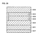
- Fig. 36 is a longitudinal sectional view illustrating a configuration of one pixel of the conventional organic EL element.
- the conventional organic EL element is provided at least with a substrate 301, a first electrode 302 provided on the substrate 301, an organic EL layer 303, and a second electrode 304.
- barriers 305 be provided on side-edge portions of the organic EL layer 303 and the second electrode 304. Further, for the sake of contrast, it is preferable that a polarizer 307 be provided on that surface of the substrate 301 which does not face to the first electrode 302. Further, for the sake of reliability, it is preferable that a sealing film or a sealing substrate 306 be provided on the second electrode 304.
- the organic EL layer 303 may be a single-layered structure including only an organic light emitting layer, or a multilayered structure including a charge transport layer (electron transport layer or a hole transport layer) and the organic light emitting layer.
- a photoresist method is conventionally known as a method for manufacturing the organic EL layer in the organic EL display device.
- a black matrix hereinafter referred to as BM
- BM black matrix
- a spinner an entire surface of the glass substrate is coated with a photosensitive resin in which a pigment of a predetermined color is dispersed.
- the photosensitive resin is then dried, and is subjected to exposure and development. In this way, a color pixel pattern of the predetermined color is obtained.
- This process is repeated three times, i.e., for each of three colors R, G, and B (Red, Blue, and Green), so as to form an organic EL pattern.
- the foregoing method has a problem in that a previously-formed organic EL layer is easily damaged in a photolithography process for forming a successively-formed organic EL layer. Further, an organic EL material needs to be also applied to a non-desirable position. This caused a material cost to increase. Further, the photolithography process is disadvantageous in terms of production costs, because (I) production facility therefor is expensive, and (II) the photolithography process is not so flexibly adjustable to allow any change in design.
- Japanese Laid-Open Patent Application No. 10-12377/1998 discloses a technique for patternizing a light emitting layer by using an inkjet method.
- the foregoing publication discloses a method for manufacturing an organic EL layer, in which inks of R, G, and B are respectively printed only in predetermined positions of the glass substrate, thereby forming a color pixels pattern.
- the inkjet method With the inkjet method, it is possible to form layers for three primary colors R, G, and B simultaneously. This prevents the organic EL element from being damaged by the repeating photolithography process, and allows reduction of a production time. Further, since the ink is only applied to a position of the color pixel, an amount of the pigment used becomes less than the amount used in the photolithography method. Thus, it is possible to realize a remarkable reduction of the material cost. Further, since it is not necessary to carry out the complicate exposure and development, a developing apparatus becomes no longer necessary. Therefore, the manufacturing cost is reduced. Moreover, since it is possible to work under a normal temperature and a normal pressure, the inkjet method appears to be more promising in improving a productivity, and in simplifying the productive facility.
- a landed droplet is positionwise restricted by forming a liquid-affinitive region and a liquid-repellent region on a top surface of the substrate.
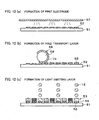
- the organic EL layer is formed by a formation method as described hereinbelow with reference to Figs. 37(a) to 37(c) .
- a liquid-affinity treatment is carried out with respect to the entire surface of a substrate 311.
- a liquid-repellent region 313 is formed by carrying out the photolithography process, the liquid-repellent region 313 having a line width of 10 ⁇ m between pixels adjacent to each other, where a size of one pixel is 120 ⁇ m ⁇ 100 ⁇ m by way of example.
- a liquid-affinitive region 312 and the liquid-repellent region 313 are segmented from each other as illustrated in Fig. 37(a) .
- an ink droplet 314 is ejected toward the liquid-affinitive region 312.
- the droplet 314 landed on the substrate 311 does not spread out in the liquid-repellent region 313, and is retained in the liquid-affinitive region 312.
- a solvent of the droplet 314 is dried off, thereby forming the organic EL layer.
- a size of a single droplet is 105 ⁇ m.
- the droplet 314 is extended by 1.5 times of a diameter thereof due to an impact caused by landing on the substrate 311. Therefore, as illustrated in Fig. 37(b) , a part of the landed droplet 314 is spread out beyond the liquid-repellent region 313 (that serves as an external frame of the pixel), and reaches the liquid-affinitive region 312 of the next pixel.
- the ink which is a part of the landed droplet 314 moves to the other liquid-affinitive region 312 before the droplet 314 dries, the ink will not return to the pixel (liquid-affinitive region 312) on which the droplet 314 originally has landed. This causes the droplet 314 to split as illustrated in Fig. 37(c) .
- the diameter of the single droplet is an option to avoid the foregoing problem.
- the thickness of the organic EL layer formed by the single droplet 314 is 0.02 ⁇ m. This is less than a half of the desirable thickness. Therefore, the droplet 314 needs to be ejected toward the same pixel twice or more.
- successive droplets land on the organic EL layer formed by a previously landed droplet. Since the organic EL layer formed by the previously landed droplet is not subjected to the liquid-affinity treatment, the successive droplets do not spread out in a desirable shape. This causes an unevenness. Further, if the successive droplets land before the previous droplet dries, the ink will spread out to the liquid-affinitive region 312 of the next pixel.
- an option is to form a barrier around the pixel so as to prevent the ink to spread out beyond the barrier.
- a method for forming the organic EL layer using such a technique is described with reference to Figs. 38 and 39 .
- BM black matrix
- this BM be used as a barrier for blocking the spreading-out of the droplet 314 containing the organic EL material ( Fig. 38(a) ).
- the foregoing method of utilizing the barrier 315 causes the uneven thickness of the organic EL layer 316 formed after the droplet 314 dries.
- the organic EL layer 316 is thin at its central portion and thick at a portion along the barrier 315.
- This uneven thickness must be avoided, because it largely affects a color property of the organic EL display.
- a liquid-repellency treatment be carried out with respect to the barrier 315 in order to avoid an adhesion of the ink to the barrier 315.
- the method does not yet solve the problem of the depression at the center portion.
- the method using the barrier 315 also has the following problems.
- the droplet 314 should contain the organic EL material of a volume corresponding to (1 pixel area ⁇ thickness), the organic EL material dissolved in the droplet 314.
- a size of a display region is 120 ⁇ m ⁇ 100 ⁇ m
- the thickness of the substrate 311 is 0.05 ⁇ m.
- the diameter of the droplet is required to be 105 ⁇ m where it is supposed that the volumetric concentration of the organic EL material is 0.1%. Therefore, a height of the BM (barrier 315) needs to be 1000 times of the thickness of the organic EL layer. This not only causes waste of the BM material, but also affects an overall design of an organic EL display apparatus.
- the foregoing problem is not solved by merely reducing the diameter of the droplet, if the levels of the BM and the organic EL layer is kept equal to each other.
- the size of the single droplet must be reduced to 10 ⁇ m.
- the droplet of a smaller size is more largely affected by an air resistance while it is flying in the air. Therefore, a flying speed of the droplet slows down, and a landing accuracy is deteriorated.
- a volume of an unfilled portion within the barrier 315 decreases as a solute content of the previous droplet 314 (previous-droplet-substance 317 to be cured) is deposited on a bottom portion within the barrier 315. This causes the droplet landing afterward to flow out of the barrier 315 as illustrated in Fig. 39(b) .
- one option is to increase concentration of the droplet 314, and eject the droplets 314 at sufficiently long intervals, so that the solvent of the previous droplets is dried off by the time a final droplet is landed.
- concentration of the droplet 314 the higher the concentration of the droplet becomes, the higher viscosity the ink has so as to be unable to be ejected by using a conventional inkjet method.
- a liquid crystal array is conventionally manufactured by the following manufacturing process. First, on one of a pair of transparent glass substrates, a liquid crystal driving element, such as a TFT (thin film Transistor) is formed. Then, a transparent electrode and an alignment film are formed and spacers are applied on the one of the substrates. Next, this substrate is assembled together with another substrate on which a colored color filter, a transparent electrode and an alignment film are formed. Then, liquid crystal is injected into a gap formed by the spacers between the substrates, and the substrates are sealed off.
- a liquid crystal driving element such as a TFT (thin film Transistor) is formed.
- TFT thin film Transistor
- silica or plastic particles of several micrometers are usually spread out as the foregoing spacers.
- the spacers are placed also in aperture areas (region for controlling transmission and reflection of light) of the liquid crystal array. Further, the spacers are placed unevenly in terms of its number and position. This causes the aperture ratio to decrease, thereby resulting in a poor displaying quality or an uneven display.
- spacers are arranged and formed on a black matrix (BM) of a color filter substrate.
- Japanese Laid-Open Patent Application No. 281562/1993 discloses a method in which liquid crystal mixed with a spacer material is (A) heated by using a heater and stirred by using a stirring device at the same time, and (B) ejected toward a liquid crystal substrate by using an inkjet apparatus having a nozzle of 60 ⁇ m in nozzle diameter.
- the ejection of the liquid crystal by using the inkjet method is made possible by heating the liquid crystal so as to lower viscosity of the liquid crystal. This allows the spacer material to be evenly spread out immediately when the liquid crystal is dropped.
- the spacers are formed by (I) plotting a spacer pattern by using the inkjet method for applying, on a substrate, a spacer forming material in a form of ink, and (II) curing the spacer forming material.
- the method for forming the spacer by using the conventional inkjet apparatus has the following problem.
- a higher concentration of the spacer forming material causes a higher viscosity of the spacer forming material.
- Typical inkjet methods such as a bubble-jet method or a piezo-electric method are usually arranged such that a viscosity of a substance that can be ejected is about 2 to 20 Pc and a substance having a viscosity higher than this range cannot be ejected therefrom.
- the viscosity of the ink to be ejected is decreased by heating a vicinity of the nozzle.
- the spacer forming material may be cured within the nozzle and clog the nozzle, in a case where a curable resin is used as the spacer material.
- the spacer forming material includes 10 wt% of copolymer, 80 wt% of water, and 10 wt% of ethylene glycol. After the spacer forming material is dried, a volume of the spacer forming material becomes a fraction of an original volume thereof.
- shapes of the spacers being formed is, for example, a flat shape of 5 ⁇ m in thickness, and 50 ⁇ m in diameter.
- the problem of the spacer-caused decrease in the aperture ratio is not solved.
- due to the low concentration it is necessary to carry out baking at 100°C for 15 min., then at 200 °C for 30 min. Therefore, it takes longer time to form the spacer.
- the droplet containing the spacer material lands on the ink substrate, the droplet moves before the solvent is dried off. Therefore, the spacers are not formed in a desirable position.
- a needed thickness of the spacer for the BM of 10 ⁇ m in width is 5 ⁇ m, and that the concentration of the spacer forming material (ink) is allowed to be as high as 50%. It is further supposed that the liquid-repellency treatment is carried out with respect to a surface of the BM, and that, after the droplet of the liquid lands, the droplet is not spread out, and an area of the liquid is maintained to be within 1.5 times of the diameter of the droplet.
- the droplet can be as large as ⁇ 6.7 ⁇ m.
- the thickness of the spacer material remaining after the solvent is dried off is 1 ⁇ m, and is below the targeted thickness. Accordingly, it is necessary to laminate the spacer material by carrying out repeated ejections. In this case, the solvent of the previous droplet must be completely dried off before the successive droplet is ejected, otherwise the droplet will be spread out. As a result, in repeated ejection, ejection intervals (time intervals between ejections) becomes long, and a working efficiency is deteriorated.
- the concentration of the spacer forming material (ink) needs to be even higher, and a configuration capable of ejecting a droplet of such a highly concentrated spacer forming material (ink) is required.
- Japanese Laid-Open Patent Application No. 2000-246887 discloses the following technology. Namely, the foregoing application discloses a method for ejecting a highly viscous substance by using a dispenser.
- an electrode is arranged entirely or partially on a container in which a highly viscous substance of 100 cps to 1,000,000 cps is filled in.
- This container has, at its bottom section, a polygonal or circular orifice of 50 ⁇ m to 1 mm in diameter. From the orifice, the highly viscous substance is protruded out forming a meniscus. Then, the highly viscous substance protruded forming the meniscus is pulled out by applying a voltage to the electrode. Next, a part of the substance is cut off to separate, and is adhered to a medium.
- This technology utilizes a fact that the meniscus from the nozzle forms a conical shape with an application of a voltage.
- a larger pulse amplitude forms a higher conical-shape of the meniscus. Therefore, the larger pulse amplitude increases a volume of that portion of the meniscus which is extended toward a substrate and is to touch the substrate, and thus attains a larger dot diameter.
- the spacers are formed by laminating the spacer forming material (ink), a distance between a recording-subjected side member and the nozzle gradually becomes shorter, as the spacers are being laminated. Therefore, controlling of the dot diameter becomes very difficult. Further, as to stabilizing an amount of the ink being applied, it is necessary to enlarge the pulse so that not only the leading edge of the conical-shape meniscus but also a vicinity of a middle of the meniscus is abutted against the substrate. Therefore, the diameter of the droplet should be at least a half of the diameter of the nozzle or more.
- the diameter of the nozzle In order to reduce the dot diameter in this situation, the diameter of the nozzle must be reduced. However, in this case, the nozzle-to-substrate distance must be shortened at the same time. This causes larger influences from errors in the nozzle-to-substrate distance, caused by the uneven thickness of the substrate or a wavy shape of the substrate. Thus a stable ejection becomes difficult.
- Recent advancement in information network leads to increasing demands for a thin, lightly-weighted, and low-power-consuming display element. Under such circumstances, a bright and low-voltage-driven liquid crystal display has received much attention.
- a color liquid crystal display is so arranged that a transmission amount of light emitted from a backlight is controlled by controlling alignment of liquid crystal by using a transparent electrode (ITO film) connected to a TFT.
- ITO film transparent electrode
- passing of the light through a color filter causes a color to appear.
- one pixel sometimes means a group of plural color filters, such as a set of R, G, and B. However, in this specification, “one pixel” denotes one color filter.
- spin-coat method has been known as one of method for manufacturing a color filter substrate.
- a black matrix (Hereinafter referred to as BM) made of a metal such as chrome is formed on a glass substrate by photolithography and etching.
- a spinner an entire surface of the glass substrate is coated with a photosensitive resin in which a pigment of a predetermined color is dispersed.
- the photosensitive resin is then dried, and is subjected to exposure and development. In this way, a color pixel pattern of the predetermined color is obtained.
- This process is repeated three times, i.e., for each of three colors R, G, and B (Red, Blue, and Green), so as to form a color filter pattern.
- Japanese Laid-Open Patent Application No. 75205/1984 discloses a technique for patternizing a color filter by using the inkjet method.
- the technology relates to a method for manufacturing the color filter substrate, in which inks of R, G, and B are respectively printed only in predetermined positions of the glass substrate, thereby forming the color pixels.
- the inkjet method With the inkjet method, it is possible to form layers for three primary colors R, G, and B simultaneously. Therefore, it is possible to reduce the production time. Further, since the ink is only applied to a position of the color pixel, an amount of the pigment used becomes less than the amount used in the spin coat method. Thus, it is possible to realize a remarkable reduction of the material cost. Further, since it is not necessary to carry out the complicate exposure and development, a developing apparatus becomes no longer necessary. Therefore, the manufacturing cost is reduced. Moreover, since it is possible to work under a normal temperature and a normal pressure, the inkjet method appears to be more promising in improving the productivity, and in simplifying the productive facility.
- a dispersion preventing pattern is formed on a substrate, by using a substance having a poor wettability.
- ink containing the pigment is applied by using the inkjet method, thereby forming the color filter.
- the color filter layer is formed by a formation method as described hereinbelow with reference to Figs. 37(a) to 37(c) .
- a liquid-affinity treatment is carried out with respect to the entire surface of a substrate 311.
- a liquid-repellent region 313 is formed by carrying out the photolithography process, the liquid-repellent region 313 having a line width of 10 ⁇ m between pixels adjacent to each other, where a size of one pixel is 300 ⁇ m ⁇ 100 ⁇ m by way of example.
- a liquid-affinitive region 312 and the liquid-repellent region 313 are segmented from each other as illustrated in Fig. 37(a) .
- an ink droplet 314 is ejected toward the liquid-affinitive region 312.
- the droplet 314 landed on the substrate 311 does not spread out in the liquid-repellent region 313, and is retained in the liquid-affinitive region 312.
- a solvent of the droplet 314 is dried off, thereby forming the color filter layer.
- a size of a single droplet is 105 ⁇ m.
- the droplet 314 is extended by 1.5 times of a diameter thereof due to an impact caused by landing on the substrate 311. Therefore, as illustrated in Fig. 37(b) , a part of the landed droplet 314 is spread out beyond the liquid-repellent region 313 (that serving as an external frame of the pixel), and reaches the liquid-affinitive region 312 of the next pixel.
- the ink which is a part of the landed droplet 314 moves to the other liquid-affinitive region 312 before the droplet 314 dries, the ink will not return to the pixel (liquid-affinitive region 312) on which the droplet 314 originally has landed. This causes the droplet 314 to split as illustrated in Fig. 37(c) .
- the diameter of the single droplet is an option to avoid the foregoing problem.
- the thickness of the color filter layer formed by the single droplet 314 is 0.45 ⁇ m. This is less than a half of the desirable thickness. Therefore, the droplet 314 needs to be ejected toward the same pixel twice or more.
- successive droplets land on the color filter layer formed by a previously landed droplet. Since the color filter layer formed by the previously landed droplet is not subjected to the liquid-affinity treatment, the successive droplets do not spread out in a desirable shape. This causes an uneven thickness. Further, if the successive droplets land before the previous droplet dries, the ink will spread out to the liquid-affinitive region of the next pixel.
- an option is to form a barrier around the pixel so as to prevent the ink to spread out beyond the barrier.
- a method for forming the color filter layer using the technique is described with reference to Figs. 38 and 39 .
- a black matrix (Hereinafter referred to as BM) is formed for obtaining a clear contrast of the pixels. It is suggested that this BM be used as the barrier 315 for blocking the spreading-out of the droplet 314 containing the color filter material ( Fig. 38(a) ).
- the foregoing method of utilizing the barrier 315 causes the uneven thickness of the color filter layer 316 formed after the droplet 314 dries.
- the color filter layer 316 is thin at its central portion, and the color filter layer 316 is thick at a portion along the barrier 315.
- This uneven thickness must be avoided, because it largely affects a color developing property of the color filter layer 316.
- a liquid-repellency treatment be carried out with respect to the barrier 315 in order to avoid an adhesion of the ink to the barrier 315. The method, however, does not yet solve the problem of the depression at the center portion.
- the method using the barrier 315 also has the following problems.
- the droplet 314 should contain the color filter material of a volume corresponding to (1 pixel area ⁇ thickness), the color filter material dissolved in the droplet 314.
- a size of a display region is 300 ⁇ m ⁇ 100 ⁇ m
- the thickness of the color filter layer is 1 ⁇ m.
- the diameter of the droplet is required to be 105 ⁇ m where the volumetric concentration of the color filter material is 5%. Therefore, a height of the BM (barrier 315) needs to be 20 times of the thickness of the color filter layer. This not only causes waste of the BM material, but also affects an overall design of a liquid crystal element.
- the foregoing problem is not solved by merely reducing the diameter of the droplet, if the levels of the BM and the color filter layer is kept equal to each other.
- the size of the single droplet must be reduced to 20 ⁇ m.
- the droplet of a smaller size is more largely affected by an air resistance while it is flying in the air. Therefore, a flying speed of the droplet slows down, and a landing accuracy is deteriorated. Further, as illustrated in Fig.
- a volume of an unfilled portion within the barrier 315 decreases as a dissolved substance of the previous droplet 314 (previous-droplet-substance 317 to be cure) is deposited on a bottom portion within the barrier 315. This causes the droplet landing afterward to flow out of the barrier 315.
- one option is to increase the concentration of the droplet 314, and eject the droplet 314 at sufficiently long intervals, so that the solvent of the previous droplets dry by the time a final droplet is landed.
- the higher the concentration of the droplet becomes the higher viscosity the ink has so as to be unable to be ejected by using a conventional inkjet method.
- an object of the present invention is to provide an active matrix organic EL display element, and an active matrix organic EL display element manufacturing method, for forming an organic EL layer, in which a drying rate of a landed droplet is taken into account, so that the organic EL layer is formed in an accurate position, and advantages of an inkjet method is utilized, without particular needs of a barrier, a liquid-repellent region, and a liquid-affinitive region around the pixel.
- the present invention is made for solving the foregoing problems, and it is also an object of the present invention to provide a liquid crystal array and a liquid crystal array manufacturing method utilizing an arrangement that allows accurate application and formation of spacers, for example, boundary between aperture sections on a substrate (such as a TFT substrate, a color filter substrate, or the like) having the aperture sections per pixel.
- the method of the present invention prevents spacer-caused decrease in an aperture ratio and easily obtains the spacers having desirable thicknesses (heights).
- an object of the present invention is to provide a color filter substrate, and a color filter substrate manufacturing method, for forming a color filter, in which a drying rate of a landed droplet is taken into account, so that the color filter is formed in an accurate position, and advantages of an inkjet method is utilized, without particular needs of a barrier, a liquid-repellent region, and a liquid-affinitive region around the pixel.
- a minute droplet forming apparatus comprises a nozzle for storing therewithin a liquid for forming a droplet, a substrate disposed so as to face the tip of the nozzle, for mounting the droplet dropped from the tip of the nozzle, and a pulse power supply for applying a pulse voltage between an electrode arranged in the liquid within the nozzle and the substrate.
- a piece of nickel disposed within the nozzle is moved to the tip part of the nozzle by way of a magnet, so as to enhance the fluid resistance in the nozzle tip part, thereby causing a setback force for returning the liquid into the nozzle, by which the droplet is isolated from the liquid column.
- JP 8212925 A discloses fluorescent screen forming method and a fluorescent screen forming device as well as a respective fluorescent sreen ink.
- a nozzle of an ink jet system is used to deliver ink containing a fluorescent screen substance and a fluorescent screen is formed.
- an electric charge control system ink jet mechanism is employed comprising an electro-mechanical conversion system and an electrically/ thermal conversion system, etc.
- An opening position of a shadow mask is optically detected in order to calculate a prescribed position of delivering ink so as to form the fluorescent screen corresponding to the opening position.
- JP 2002365424 A discloses an apparatus for providing droplets onto a substrate.
- the inventors of the present invention made diligent studies on a technique to enable (i) control of movement amount of a droplet after the droplet ejected from a nozzle is landed and before the landed droplet is dried, (ii) accurate and easy formation of an organic EL layer having a thick thickness.
- the inventors predicted that a certain combination of parameters such as droplet diameter of a liquid (ink) containing an organic EL layer material gives a region in which the droplet (ink) is dried immediately after landing. Further, the inventors accomplished an inkjet method that allows ejection under such condition.
- a method of the present invention is for producing an active matrix organic EL display element by an inkjet method to eject droplets of a liquid via an ejection hole of a nozzle so as to form an organic EL layer, the liquid containing an organic EL layer material.
- the method of the present invention is arranged such that an electrostatic attraction type inkjet apparatus is used whose ejection hole has a diameter smaller than a diameter of the droplets; and the droplets are ejected from the nozzle of the electrostatic attraction type inkjet apparatus in such a manner that each of the droplets is 1pl or less in amount.
- an apparatus of the present invention is for producing an active matrix organic EL display element, the apparatus adopting an inkjet method to eject droplets of a liquid via an ejection hole of a nozzle so as to form an organic EL layer, and the liquid containing an organic EL layer material.
- the apparatus of the present invention is arranged such that the ejection hole of the nozzle has a diameter smaller than a diameter of the droplets, the inkjet method is of electrostatic attraction type, and each of the droplets ejected via the nozzle is 1pl or less in amount.
- the droplet dries immediately after landed on an organic EL layer formation region on a substrate. This makes it difficult for the droplet to move after landing on the substrate, thereby making it possible to form the organic EL layer with accurate positioning.
- a plurality of the droplets are ejected to form an organic EL layer having a predetermined thickness by forming lamination with the droplets.
- the method of the present invention allows the inkjet method to effectuate its advantage, and especially makes it possible to form the organic EL layer easily and with low cost without forming (i) a barrier around the organic EL layer formation region (pixel region), (ii) liquid-repelling region and liquid-affinitive region, and the like.
- the user of the electrostatic attraction type inkjet device whose nozzle has a diameter smaller than the diameter of the droplet makes it possible to eject the droplet with a minute diameter of 1pl or less, while keeping the applied voltage for generating an electric field used for performing electrostatic attraction type.
- the ejection of the droplet can be stably performed because in the use of the electrostatic attraction type inkjet device the electric charge can be easily concentrated in the droplets in ejecting and thus variation of an electric field strength around the droplet becomes small. As a result, it becomes possible to repeatedly eject the droplet in high-frequency ejection operation, thereby improving production efficiency.
- the amount of the droplet may be 1pl or less. Moreover, it is necessary in the production of the organic EL display element that the concentration of the organic EL layer be not less than a predetermined value after the application of the droplet. Therefore, in case where a minute droplet is used as in the present invention, the ejection of the droplet is carried out with respect to a same organic EL layer formation region in plural times.
- the liquid may be used whose volumetric concentration is determined from a number of layers formed with the droplets by repeating the ejection onto the same organic EL layer formation region.
- a method of the present invention is for producing an active matrix organic EL display element by an inkjet method to eject droplets of a liquid via an ejection hole of a nozzle so as to form an organic EL layer, the liquid containing an organic EL layer material.
- the method of the present invention is arranged such that an electrostatic attraction type inkjet apparatus is used, the electrostatic attraction type inkjet apparatus being for ejecting droplets via its nozzle in such a manner that, each of the droplets is 1pl or less in amount; and the liquid has a volumetric concentration ⁇ (%) that is substantially ⁇ ' t/( ⁇ ' D), where ⁇ is a number of layers to be formed with the droplets repeatedly ejected on a same organic EL layer formation region, ⁇ is a value obtained from a ratio between the diameter of the droplets and a diameter of landed droplets in the organic EL layer formation region, D is the diameter of the droplets, and t is a thickness of the organic EL layer to be formed.
- an apparatus of the present invention is for producing an active matrix organic EL display element, the apparatus adopting an inkjet method to eject droplets of a liquid via an ejection hole of a nozzle so as to form an organic EL layer, and the liquid containing an organic EL layer material.
- the apparatus of the present invention is arranged such that the inkjet method is of an electrostatic attraction type and each of the droplets ejected is 1pl or less in amount; and the liquid has a volumetric concentration ⁇ (%) that is substantially ⁇ ' t/( ⁇ ' D), where ⁇ is a number of layers to be formed with the droplets repeatedly ejected on a same organic EL layer formation region, ⁇ is a value obtained from a ratio between the diameter of the droplets and a diameter of landed droplets in the organic EL layer formation region, D is the diameter of the droplets, and t is a thickness of the organic EL layer to be formed.
- the droplet dries immediately after landed on an organic EL layer formation region on a substrate. This makes it difficult for the droplet to move after landing on the substrate, thereby making it possible to form the organic EL layer with accurate positioning.
- a plurality of the droplets are ejected to form an organic EL layer having a predetermined thickness by forming lamination with the droplets.
- the method of the present invention allows the inkjet method to effectuate its advantage, and especially makes it possible to form the organic EL layer easily and with low cost without forming (i) a barrier around the organic EL layer formation region (pixel region), (ii) liquid-repelling region and liquid-affinitive region, and the like.
- the increase in the number of the layer prolongs operation time. Therefore, the volumetric concentration of the liquid (ink) is set to be high, satisfying the above equation. This reduces the number of the layers of the lamination, thereby reducing the number of the times of ejection and improving the production efficiency.
- the approximation range may be, for example, ⁇ 10%, taking unevenness of the amount of the droplets into consideration.
- the method for producing the active matrix organic EL display element may be arranged such that the ejection hole of the electrostatic attraction type inkjet apparatus is smaller than the liquid crystal in diameter.
- the arrangement it is possible to eject a minute droplet of 1pl or less, but a low applied voltage still can be used for generating the electric field for electrostatic attraction. Moreover, the electric charge can be easily concentrated in the droplet in ejecting the droplet. Thus, the variation of the ambient electric field intensity around the droplet becomes small. Thus, stable ejection is attained. As a result, it becomes possible to release the droplet continuously, with ejection driving using a high frequency. This improves productivity.
- the method for producing the active matrix organic EL display element may be arranged such that the liquid has a viscosity of 20cP or more.
- the use of the highly viscous ink having viscosity of 20cP or more as the liquid (ink) reduces the number of the layers to be made with the plurality of droplets.
- the number of ejection is reduced, thereby improving the productivity.
- the method for producing the active matrix organic EL display element may be arranged such that the organic EL layer has an organic light emitting layer.
- the method for producing the active matrix organic EL display element may be arranged such that the organic EL layer has a charge transport layer.
- a method of the present invention is for producing a liquid crystal array having a pair of substrates facing each other and having a gap in which a liquid crystal is filled, the gap formed by a spacer provided between the substrates, at least one of the substrates having an aperture section, and the method comprising the steps of (i) ejecting droplets of a spacer material via an ejection hole of the nozzle by an inkjet method, and (ii) curing the spacer material so as to form the spacer.
- the method is arranged such that the ejection hole of the nozzle has a diameter smaller than a diameter of the droplets, the inkjet method is of electrostatic attraction type, and each of the droplets ejected via the nozzle is 1pl or less in amount.
- the aperture section is a region used for controlling light transmission or light reflection of a display section.
- the droplet dries immediately after landing on a spacer formation surface of the substrate. Therefore, it is difficult for the droplet to move after it landed on the substrate. Thus, it is possible to form the space with accurate positioning.
- a plurality of droplets are ejected to make a lamination in order to form a spacer having a desirable thickness. In this case, it is possible to avoid a problem in that a droplet landed successively is moved due to influence from a droplet landed previously.
- the present invention allows to utilizes the advantage of the inkjet method, thereby making it possible to easily and inexpensively form the spacer having a desired thickness, but without reducing the aperture ratio of the liquid crystal array.
- the electrostatic attraction type inkjet apparatus whose nozzle has the ejection hole having the diameter smaller than the diameter of the droplet, it is possible to eject a minute droplet of 1pl or less, but a low applied voltage still can be used for generating the electric field for electrostatic attraction.
- the electric charge can be easily concentrated in the droplet in ejecting the droplet.
- the variation of the ambient electric field intensity around the droplet becomes small.
- stable ejection is attained.
- the amount of the liquid can be 1pl or less.
- the thickness of the spacer should not be less than a predetermined value. In cases where a minute droplet is used as in the present invention, the ejection of the droplet is repeated in plural times with respect to a same spacer formation place.
- a method of the present invention is for producing a liquid crystal array having a pair of substrates facing each other and having a gap in which a liquid crystal is filled, the gap formed by a spacer provided between the substrates, at least one of the substrates having an aperture section, the method comprising the steps of (i) ejecting droplets of a spacer material via an ejection hole of the nozzle by an inkjet method, and (ii) curing the spacer material so as to form the spacer.
- the method of the present invention includes causing a tip portion of the nozzle to be in contact with a spacer formation surface of a substrate; applying a voltage to an electrode of the nozzle being in contact with the spacer formation surface, so as to shrink the spacer material; and release the spacer material continuously, via the nozzle under the voltage application as the nozzle is moved away from the substrate, so as to form, on the substrate, the spacer having a column-like shape.
- the present invention allows to utilizes the advantage of the inkjet method, thereby making it possible to easily and inexpensively form the spacer having a desired thickness, but without reducing the aperture ratio of the liquid crystal array.
- the method for producing the liquid crystal array may be arranged such that the ejection hole of the nozzle has a diameter of 8 ⁇ m or less. This arrangement allows stable formation of the spacer.
- a method of the present invention is for producing a liquid crystal array having a pair of substrates facing each other and having a gap in which a liquid crystal is filled, the gap formed by a spacer provided between the substrates, at least one of the substrates having an aperture section.
- the method of the present invention includes ejecting, by using an electrostatic attraction type inkjet apparatus, droplets of a liquid onto a spacer formation surface via a nozzle of the electrostatic attraction type inkjet apparatus so as to form the spacer, the nozzle having an ejection hole having a diameter smaller than a diameter of the droplets, the liquid comprising a solid spacer, and each of the droplets being 1pl or less in amount.
- the droplet dries, i.e., a solvent is dried off immediately after landing. Therefore, it is difficult for the solid spacer contained in the droplet to move after the droplet landed on the spacer formation surface. Thus, it is possible to form the spacer with accurate positioning. With this, it is possible to avoid the reduction of the aperture ratio in the liquid crystal array. Moreover, because the solvent dries immediately after the droplet is landed, no such problem occurs that the solvent remained on the substrate adversely affects an alignment film or the like.
- the electrostatic attraction type inkjet apparatus whose nozzle has the ejection hole having the diameter smaller than the diameter of the droplet, it is possible to eject a minute droplet of 1pl or less, but a low applied voltage still can be used for generating the electric field for electrostatic attraction. Moreover, the electric charge can be easily concentrated in the droplet in ejecting the droplet. Thus, the variation of the ambient electric field intensity around the droplet becomes small. Thus, stable ejection is attained. As a result, it becomes possible to perform accurate positioning control as to position in which the spacer is formed.
- the present invention allows to utilizes the advantage of the inkjet method, thereby making it possible to easily and inexpensively form the spacer having a desired thickness, but without reducing the aperture ratio of the liquid crystal array.
- a method of the present invention is for producing a liquid crystal array having a pair of substrates facing each other and having a gap in which a liquid crystal is filled, the gap formed by a spacer provided between the substrates, at least one of the substrates having an aperture section.
- the method of the present invention is arranged such that it includes, after providing an individual spacer on a spacer providing surface, positioning the individual spacer by hitting the solid spacer with a droplet ejected via a nozzle of an electrostatic attraction type inkjet apparatus so as to move the solid spacer, the nozzle having an ejection hole having a diameter smaller than a diameter of the droplet, and the droplet being 1pl or less in amount.
- the position of the solid spacer can be adjusted by ejecting of the droplet from the nozzle, thereby solving such conditions such as grouping of spacers in one place. Therefore, it is possible to avoid reduction of the aperture ratio.
- the amount of the single droplet ejected from the nozzle is 1pl or less, the droplet dries immediately after the droplet is landed. Therefore, no such problem occurs that the solvent remained on the substrate adversely affects an alignment film or the like.
- the electrostatic attraction type inkjet apparatus whose nozzle has the ejection hole having the diameter smaller than the diameter of the droplet, it is possible to eject a minute droplet of 1pl or less, but a low applied voltage still can be used for generating the electric field for electrostatic attraction. Moreover, the electric charge can be easily concentrated in the droplet in ejecting the droplet. Thus, the variation of the ambient electric field intensity around the droplet becomes small. Thus, stable ejection is attained. As a result, it becomes possible to perform accurate positioning control as to position in which the spacer is formed.
- the present invention allows to utilizes the advantage of the inkjet method, thereby making it possible to easily and inexpensively form the spacer having a desired thickness, but without reducing the aperture ratio of the liquid crystal array.
- the method for producing the liquid crystal array maybe arranged such that a material ejected from the nozzle has a viscosity of 30cP or more.
- the viscosity of the ejected material from the nozzle is so high, i.e. 30cP or more, it is possible to surely increase drying rate of the solvent in the ejected material after landing. This surely improves positional accuracy of the spacer.
- the number of times of ejections i.e. the number of the layers in the lamination increase because thickness of a spacer formed with the single droplet is thin. This increase production time.
- the high concentration of the droplet (ejected material) can suppresses the increases in the number of times of ejections, i.e. the number of the layers in the lamination. As a result, productivity can be improved.
- that substrate on which the spacer is to be formed may be configured such that a color filter is formed on a transparent substrate, the color filter colored with at least three colors or more.
- That substrate on which the spacer is to be formed is an active matrix substrate in which an active element is provided per pixel.
- the inventors of the present invention made diligent studies on a technique to enable (i) control of movement amount of a droplet after the droplet ejected from a nozzle is landed and before the landed droplet is dried, (ii) accurate and easy formation of a color filter having a thick thickness.
- the inventors predicted that a certain combination of parameters such as droplet diameter of a liquid (ink) containing a color filter layer material gives a region in which the droplet (ink) is dried immediately after landing. Further, the inventors accomplished an inkjet method that allows ejection under such condition.
- a method of the present invention is for producing a color filter substrate, the method comprising ejecting droplets of a liquid via an ejection hole of a nozzle by an inkjet method so as to form a color filter layer, and the liquid comprising a color filter layer material.
- the method of the present invention is arranged such that an electrostatic attraction type inkjet apparatus is used whose ejection hole is smaller than a diameter of the droplets; and the droplets are ejected from the nozzle of the electrostatic attraction type inkjet apparatus in such a manner that each of the droplets is 1pl or less in amount.
- an apparatus of the present invention is for producing a color filter layer substrate, the apparatus adopting an inkjet method to eject droplets of a liquid via an ejection hole of a nozzle so as to form a color filter layer, and the liquid comprising a color filter layer material.
- the apparatus of the present invention is arranged such that the ejection hole of the nozzle has a diameter smaller than a diameter of the droplets, the inkjet method is of electrostatic attraction type, and each of the droplets ejected via the nozzle is 1pl or less in amount.
- the droplet dries immediately after landed on a color filter layer formation region on a substrate. This makes it difficult for the droplet to move after landing on the substrate, thereby making it possible to form the color filter layer with accurate positioning.
- a plurality of the droplets are ejected to form a color filter layer having a predetermined thickness by forming lamination with the droplets.
- the method of the present invention allows to utilize the advantage of the inkjet method and especially makes it possible to easily and inexpensively form an organic luminescent layer without requiring formation of a barrier around a color filter layer formation region (pixel region) and formation liquid-repelling region, a liquid-affinitive region and the like.
- the user of the electrostatic attraction type inkjet device whose nozzle has a diameter smaller than the diameter of the droplet makes it possible to eject the droplet with a minute diameter of 1pl or less, while keeping the applied voltage for generating an electric field used for performing electrostatic attraction type.
- the ejection of the droplet can be stably performed because in the use of the electrostatic attraction type inkjet device the electric charge can be easily concentrated in the droplets in ejecting and thus variation of an electric field strength around the droplet becomes small. As a result, it becomes possible to repeatedly eject the droplet in high-frequency ejection operation, thereby improving production efficiency.
- the amount of the droplet may be 1pl or less. Moreover, it is necessary in the production of the color filter substrate that the concentration of the color filter layer be not less than a predetermined value after the application of the droplet. Therefore, in case where a minute droplet is used as in the present invention, the ejection of the droplet is carried out with respect to a same color filter layer formation region in plural times.
- the liquid may be used whose volumetric concentration is determined from a number of layers formed with the droplets by repeating the ejection onto the same color filter layer formation region.
- a method of the present invention is for producing a color filer substrate by an inkjet method to eject droplets of a liquid via an ejection hole of a nozzle so as to form a color filter layer, the liquid comprising a color filter layer material.
- the method of the present invention is arranged such that an electrostatic attraction type inkjet apparatus is used, the electrostatic attraction type inkjet apparatus being for ejecting droplets via its nozzle in such a manner that each of the droplets is 1pl or less in amount; and the liquid has a volumetric concentration ⁇ (%) that is substantially ⁇ t/( ⁇ D), where ⁇ is a number of layers to be formed with the droplets repeatedly ejected on a same color filter layer formation region, ⁇ is a value obtained from a ratio between the diameter of the droplets and a diameter of landed droplets in the color filter layer formation region, D is the diameter of the droplets, and t is a thickness of the color filter layer to be formed.
- An apparatus of the present invention is for producing a color filter substrate, the apparatus adopting an inkjet method to eject droplets of a liquid via an ejection hole of a nozzle so as to form a color filter layer, the liquid comprising a color filter layer material.
- the apparatus of the present invention is arranged such that the inkjet method is of an electrostatic attraction type and each of the droplets ejected is 1pl or less in amount; and the liquid has a volumetric concentration ⁇ (%) that is substantially ⁇ ' t/ ( ⁇ ' D), where ⁇ is a number of layers to be formed with the droplets repeatedly ejected on a same color filter layer formation region, ⁇ is a value obtained from a ratio between the diameter of the droplets and a diameter of landed droplets in the color filter layer formation region, D is the diameter of the droplets, and t is a thickness of the color filter layer to be formed.
- the droplet dries immediately after landed on a color filter layer formation region on a substrate. This makes it difficult for the droplet to move after landing on the substrate, thereby making it possible to form the color filter layer with accurate positioning.
- a plurality of the droplets are ejected to form a color filter layer having a predetermined thickness by forming lamination with the droplets.
- the method of the present invention allows the inkjet method to effectuate its advantage, and especially makes it possible to form the color filter layer easily and with low cost without forming (i) a barrier around the color filter layer formation region (pixel region), (ii) liquid-repelling region and liquid-affinitive region, and the like.
- the increase in the number of the layer prolongs operation time. Therefore, the volumetric concentration of the liquid (ink) is set to be high, satisfying the above equation. This reduces the number of the layers of the lamination, thereby reducing the number of the times of ejection and improving the production efficiency.
- the approximation range may be, for example, ⁇ 10%, taking unevenness of the amount of the droplets into consideration.
- the method for producing the color filter substrate may be arranged such that the ejection hole of the electrostatic attraction type inkjet apparatus is smaller than the liquid crystal in diameter.
- the arrangement it is possible to eject a minute droplet of 1pl or less, but a low applied voltage still can be used for generating the electric field for electrostatic attraction. Moreover, the electric charge can be easily concentrated in the droplet in ejecting the droplet. Thus, the variation of the ambient electric field intensity around the droplet becomes small. Thus, stable ejection is attained. As a result, it becomes possible to release the droplet continuously, with ejection driving using a high frequency. This improves productivity.
- the method for producing the color filter substrate may be arranged such that the liquid has a viscosity of 20cP or more.
- the use of the highly viscous ink having viscosity of 20cP or more as the liquid (ink) reduces the number of the layers to be made with the plurality of droplets.
- the number of ejection is reduced, thereby improving the productivity.
- Fig. 1 is an electrostatic attraction type inkjet apparatus for use in manufacturing an active matrix type organic EL display element of the present embodiment.
- Fig. 1 is a longitudinal sectional view of an inkjet apparatus 15.
- the inkjet apparatus 15 is provided with a nozzle 1 for ejecting ink being stored in an ink chamber 2.
- the nozzle 1 is connected with the ink chamber 2 via a packing 3. In this way, sealing is provided so that the ink in the ink chamber 2 does not leak from a joint section of the ink chamber 2 and the nozzle 1. Further, the nozzle 1 has an orifice 1a having such a shape that a diameter of the orifice 1a gradually becomes smaller toward a side opposite to the joint section of the nozzle 1 and the ink chamber 2, i. e., toward a leading edge of the nozzle 1 from which the ink is ejected. A diameter (Hereinafter referred to as nozzle diameter) of an ejection hole 1b on the leading edge of the nozzle 1 is set on a basis of a relationship with a droplet of the ink immediately after being ejected.
- nozzle diameter A diameter (Hereinafter referred to as nozzle diameter) of an ejection hole 1b on the leading edge of the nozzle 1 is set on a basis of a relationship with a droplet of the ink immediately after being ejected
- the ink ejected from the nozzle 1 is hereinafter referred to as droplet 12, in order to distinguish the ink ejected from the nozzle 1 from the ink being stored in the ink chamber 2.
- droplet 12 A relationship between the diameter of the ejection hole 1b and a diameter of the droplet 12 immediately after being ejected are described in detail later.
- a nozzle electrode 5 for applying an electrostatic field to the ink is provided inside the nozzle 1.
- a predetermined voltage is applied from a process control section 25.
- the process control section 25 controls an electric field strength between the nozzle electrode 5 and a counter electrode 13.
- a diameter of the droplet 12 being ejected from the nozzle 1 is adjusted. Further, the droplet 12 ejected from the nozzle 1 towards the counter electrode 13 is accelerated by the electric field generated between the nozzle electrode 5 and the counter electrode 13.
- a solution of the ink filled in the ink chamber 2 is supplied via an ink supplying route 23 from an ink tank (not shown) being connected with the ink chamber 2.
- the ink chamber 2 and the nozzle 1 are kept filled with the ink, and a negative pressure is applied to the ink.
- the counter electrode 13 Toward a side facing the ejection hole 1b of the nozzle 1, the counter electrode 13 is arranged in a position which is in a predetermined distance from the nozzle 1.
- the counter electrode 13 is for electrically charging a surface of a recording treatment substrate 14 arranged on a surface facing the nozzle 1.
- the counter electrode 13 electrifies the recording treatment substrate 14 in an electric potential having the opposite polarity from a charged electric potential of the droplet 12 being ejected from the ejection hole 1b of the nozzle 1. With this arrangement, the droplet 12 ejected from the ejection hole 1b of the nozzle 1 is stably landed on the recording treatment substrate 14.
- the droplet 12 be electrically charged. Therefore, it is preferable that at least an ink ejection surface of the leading edge of the nozzle 1 be made of an insulative material. Further, since it is necessary to form the ejection hole 1b having a microscopic diameter. Thus, in the present embodiment, a glass capillary tube is used as the nozzle 1.
- the following describes a behavior of a meniscus (meniscus portion) 7 formed in the vicinity of the ejection hole 1b, when the ink is ejected as the droplet 12 from the nozzle 1.
- Figs 2(a) to 2(c) are model figures illustrating a behavior of the meniscus 7 in the vicinity of the ejection hole 1b.
- a meniscus 7a is formed in a concave-shape within the leading edge of the nozzle 1.
- a voltage applied to the nozzle electrode 5 is controlled by the process control section, in order to eject the ink 22.
- the predetermined voltage is applied to the nozzle electrode 5
- an electric charge is induced to a surface of the ink 22 in the nozzle 1, thus forming a meniscus 7b in such a shape as illustrated in Fig.
- the meniscus 7b attracted toward the outside forms a meniscus 7c in such a shape that the ink 22 is further ejected toward the counter electrode (not shown), and a droplet to be ejected is formed as a result of prevalence of (A) the electric charge induced to a surface of the meniscus 7c and a force of the electrical field (electric field strength) generated in the nozzle 1 over (B) a surface tension of the ink 22.
- the present embodiment uses the nozzle 1 whose diameter (Hereinafter referred to as nozzle diameter) of the ejection hole 1b is no more than ⁇ 8 ⁇ m (e.g. 5. ⁇ m).
- nozzle diameter of the nozzle 1 is microscopic, a curvature radius of a leading edge of the meniscus is not gradually reduced by concentrated surface electric charge, unlike a conventional case, and the curvature radius is deemed as to be constant.
- the surface tension of the droplet which the droplet has when separating off is substantially constant, in a case where the droplet is ejected with an application of the voltage. Further; an amount of the surface electric charge being concentrated surpasses the surface tension of the ink, that is, the value of the surface electric charge is no more than a value where Rayleigh separation occurs. Therefore, a maximum amount of the surface electric charge is uniformly defined.
- the electric field strength does not cause a problem, because the electric field is significantly strong only in the vicinity of the meniscus 7, and a resistance against a discharge breakdown is very high in such a high electric field in an extremely small region.
- the ink used in the inkjet apparatus 15 of the present embodiment may be dye-type ink including pure water and ink containing microparticles.
- a diameter of the microparticle contained in the ink it is necessary that a diameter of the microparticle contained in the ink be small, because the nozzle is much smaller than a conventional nozzle. In general, clogging hardly occurs with the microparticles having the diameter of approximately 1/20 to 1/100 of the nozzle diameter.
- a diameter of the microparticle in the ink will be 50 nm or less, in a case where the nozzle diameter of the nozzle 1 in the present embodiment is, for example, ⁇ 5 ⁇ m.
- the diameter of the microparticles of the ink is much smaller than a smallest diameter of conventionally used microparticles whose diameter is ⁇ 100 nm. Because of this, a moving speed of the charged microparticles in the ink is slowed down in using a method for ejecting the ink containing the microparticles such as a mechanism disclosed in Japanese Laid-Open Patent Application No. 2000-127410 ( Tokukai 2000-127410; published on May 5, 2000 ), in which (I) the electric charge of the meniscus 7 is concentrated by movement of the particulates caused by electrification of the particulates, and (II) the ink is ejected by electrostatic repulsion among the microparticles being concentrated. This causes slowing down of an ejection response speed and a recording speed.
- a method for ejecting the ink containing the microparticles such as a mechanism disclosed in Japanese Laid-Open Patent Application No. 2000-127410 ( Tokukai 2000-127410; published on
- the inkjet apparatus 15 of the present embodiment instead of ejecting the ink by using the electrostatic repulsion force among the charged microparticles, the ink is ejected by using the electric charge of a meniscus surface as in a case of using the ink not containing the microparticles.
- an electric charge amount of the microparticle be much less than the electric charge of the meniscus surface.
- the electrostatic repulsion force among the microparticles and the response speed are reduced, if the electric charge amount of the microparticles in the ink per unit mass is 10 ⁇ C/g or less. Further, a total electric charge amount of the microparticles in the ink is reduced by reducing a mass of the ink microparticle, i.e., reducing the diameter of the ink microparticle. Table 1 below indicates an ejection stability of a case where an average diameter of the microparticles in the ink is between ⁇ 3 nm to ⁇ 50 nm.
- Symbols in Table 1 indicates the ejection stability of each nozzle. ⁇ represents no ejection due to clogging or the like. ⁇ represents instable ejection when ejecting consecutively. ⁇ represents stable ejection.
- the diameter of the microparticles is preferably ⁇ 30 nm or less.
- the electric charge amount of a single grain of the microparticles in the ink is such that influence of the electric charge is almost negligible, and that the moving speed based on the electric charge is significantly slowed down. Therefore, the microparticles are not concentrated at the center of the meniscus. Further in a case where the nozzle diameter is ⁇ 3 ⁇ m or less, a maximum electric field strength is extremely high, due to concentration of the electric field at the meniscus portion. This causes an increase in an electrostatic force per grain of the microparticles.
- the ink contain the microparticles of ⁇ 10 nm or less.
- the diameter of the microparticles is less than ⁇ 1 nm, it is more likely that the microparticles are aggregated, or that the concentration becomes uneven. Therefore, the diameter of the microparticles is preferably between a range of ⁇ 1 nm to ⁇ 10 nm.
- Figs. 3(a) and 3(b) through Figs. 7(a) and 7(b) respectively illustrate distributions of electric field strength where the nozzle diameter was ⁇ 0.2, 0.4, 1, 8, or 20 ⁇ m.
- Figs. 8(a) and 8(b) respectively illustrate, for reference, a distribution of electric field strength in a case of using a conventionally used nozzle having a diameter of 50 ⁇ m.
- position of nozzle center indicates a central position of the ink ejecting surface of the ejection hole 1b of the nozzle 1.
- figures (a) indicate the distributions of the electric field strength in a case where a distance between the nozzle 1 and the counter electrode 13 was set at 2000 ⁇ m
- figures (b) indicate the distributions of the electric field strength in a case where the distance between the nozzle 1 and the counter electrode 13 was set at 100 ⁇ m.
- a same voltage of 200 V was applied.
- a distribution line in each figure was a range of the electric field strength between 1 ⁇ 106 V/m and 1 ⁇ 107V/m.
- Table 2 indicates the maximum electric field strength under each condition.
- Nozzle Diameter ( ⁇ m) Gap ( ⁇ m) Variation Rate (%) 100 2000 0.2 2.001 ⁇ 10 ⁇ 9 2.00005 ⁇ 10 ⁇ 9 0.05 0.4 1.001 ⁇ 10 ⁇ 9 1.00005 ⁇ 10 ⁇ 9 0.09 1 0.401002 ⁇ 10 ⁇ 9 0.40005 ⁇ 10 ⁇ 9 0.24 8 0.0510196 ⁇ 10 ⁇ 9 0.05005 ⁇ 10 ⁇ 9 1.94 20 0.0210476 ⁇ 10 ⁇ 9 0.0200501 ⁇ 10 ⁇ 9 4.98 50 0.00911111 ⁇ 10 ⁇ 9 0.00805 ⁇ 10 ⁇ 9 13.18
- the distance between the nozzle and the counter electrode affects the electric field strength. Accordingly, in a case where the nozzle diameter is no more than ⁇ 8 ⁇ m ( Figs. 6(a) and 6(b) ), the electric field strength is concentrated, and a change in the distance from the counter electrode barely influences the electric field strength. Thus, with the nozzle diameter of ⁇ 8 ⁇ m or less, it is possible to carry out the stable ejection regardless of positional accuracy of the counter electrode and unevenness in the thickness and material property of the recording medium.
- the electric field strength is concentrated in the center of the meniscus 7 by generating a strong electric field in a region larger than a projected area of the droplet 12 being ejected. This required that a very high voltage be applied to the nozzle electrode, thus causing difficulties in controlling a driving operation. Further, the resistance against a discharge breakdown also restricts a formable size of the minute droplet.
- the nozzle diameter is smaller than the diameter of the droplet immediately after being ejected. This allowed a region in which the electric charge is concentrated to be substantially equal to a region of the meniscus 7. As a result, the voltage applied to the nozzle electrode 5 is significantly reduced, and the electric field strength of the meniscus 7 is remarkably increased.
- the droplet 12 charged with the electric charge is appropriately accelerated by the electric field, whereby the slowing down of the droplet due to the air resistance is restrained. As a result the landing accuracy is improved. Further, by constantly applying a pressure to the inside of the nozzle 1, the meniscus 7 in a Taylor cone shape is formed on the ejection hole 1b. This causes the electric charge to be easily concentrated on the meniscus 7. Therefore, the droplet 12 can be ejected with an application of several hundred voltage to the nozzle electrode 5.
- the inkjet apparatus 15 of the present embodiment has the following features.
- a force is applied to the charged droplet 12 by the electric field generated between the nozzle electrode 5 and the counter electrode 13. Therefore, even if the influence from the air resistance increases because the droplet 12 is the minute droplet, the landing accuracy (a positional accuracy of landing on the recording-subjected-side substrate 14) of the droplet 12 is improved.
- the viscosity of ink in general is in inverse relation to a growth rate of the meniscus 7.
- High viscosity does not allow the meniscus 7 to grow in a sufficient size, and makes it impossible to eject the droplet.
- the growth rate of the meniscus 7 is not dependent on the viscosity of the ink, but is dependent on the surface tension and the amount of charge. As such, even if solute is dissolved up to a maximum solubility thereof, it is possible to eject the ink.
- the solvent of the ink is instantaneously dried off after the droplet 12 lands.
- a volume of the solvent of the droplet 12 is proportional to a power 3 of the droplet diameter. Therefore, an energy needed for evaporating the solvent is also proportional to a power 3 of the droplet diameter.
- the droplet 12 is more easily evaporated with a smaller value of (volume)/(surface area). Therefore, a smaller size of the droplet is more advantageous.
- the size of the ejected droplet is large, and a long time is needed for the solvent to be evaporated off.
- a sufficient flying speed is not obtained by merely reducing the size of the droplet to a microscopic size.
- a heat of vaporization for evaporating off the solvent content of the droplet is not obtained by merely converting a kinetic energy to a heat energy. Therefore the solvent is not instantaneously dried off after landing.
- Tables 3 through 5 indicates comparison of properties in (I) cases of using inkjet apparatuses of conventional inkjet methods, i.e., piezo-electric type, thermal type, and an electrostatic attraction type from which a droplet having a large droplet diameter is ejected, and (II) a case of using the inkjet apparatus 15 of the present embodiment in accordance with the present invention, i.e., the electrostatic attraction type inkjet apparatus 15 from which a droplet of small diameter is ejected.
- Table 3 Influence given according to the droplet volume Landing Accuracy Easiness of Ejection Drying Rate No. of Landing Droplet Vol.
- Table 3 shows the landing accuracy of the droplet 12, easiness of ejection, drying rates, and influences of the volume of the droplet to a landing number.
- the landing number is how many times the ejection needs to be carried out for forming a single pixel. In terms of production efficiency, a smaller landing number is better.
- the inkjet apparatus 15 of the present invention even the droplets having volumes of 0.1 pl and 1 pl resulted in usable or good, in terms of landing accuracy and easiness of ejection, while, in the conventional inkjet apparatuses, these droplets were not usable, in terms of all of the items. Further, in the inkjet apparatus 15 of the present embodiment, a good drying rate was obtained from the droplet having the volume of 0.1 pl and 1 pl. From the landing number, it was found that the droplet of 0.1pl is not suitable (poor production efficiency), and the droplet of 1 pl is suitable (good production efficiency).
- Table 4 shows suitability of various viscosities of the ink for the inkjet apparatus 15 of the present embodiment, and for the conventional inkjet apparatuses.
- the inkjet apparatus 15 of the present embodiment was capable of ejecting a highly viscous ink.
- P The present invention ⁇ : Good ⁇ : Ejectable ⁇ : Not suitable ⁇ : Not ejectable -: Out of applicable range
- Table 5 shows suitability of various concentrations, i.e., easiness of ejection, in the inkjet apparatus 15 and the conventional inkjet apparatuses. Table 5 also shows the drying rate and the landing number resulted from the various concentrations.
- the inkjet apparatus 15 of the present embodiment is capable of ejecting the highly viscous droplets, therefore, it is possible to eject the highly concentrated ink. As described, with a higher concentration, the number of ejections becomes less.
- an active matrix organic EL display (organic EL display system) being manufactured by using the inkjet apparatus 15 shown in Fig. 1 , and a method for manufacturing the active matrix organic EL display.
- Fig. 9 is a longitudinal sectional view illustrating a configuration of a single pixel of an organic EL element 50.
- the organic EL element is provided at least with a substrate 51, a first electrode 52 provided on the substrate 51, an organic EL layer 53, and a second electrode 54.
- a polarizing plate 57 be provided on that surface of the substrate 51 which is an opposite side with respect to the first electrode 52.
- a sealing film or a sealing substrate 56 be provided on the second electrode 54.
- the organic EL material is laminated and applied by using the foregoing inkjet apparatus 15 without causing a spreading of the droplet. Therefore, the organic EL layers of pixels adjacent to each other do not touch each other, or be mixed with each other. Further, the contrast between the pixels is made clear by causing a metal wiring (not shown) to serve as BM. Therefore, the barrier 105 formed in a conventional organic EL element shown in Fig. 22 becomes no longer necessary.
- the substrate 51 may be (I) a substrate made of an inorganic material such as a silica substrate and a glass substrate, or (II) a resin substrate such as a polyethylene terephthalate substrate, a polyether sulfone substrate, a polyimide substrate.
- a resin substrate such as a polyethylene terephthalate substrate, a polyether sulfone substrate, a polyimide substrate.
- the present invention is not limited to these.
- the organic EL layer 53 has at least one layer of an organic light emitting layer.
- the organic EL layer 53 may be a single-layered structure of an organic light emitting layer, or a multilayered structure including a charge transport layer (electron transport layer or a hole transport layer) and the organic light emitting layer. Further, the charge transport layer and the organic light emitting layer may be multilayered structure respectively.
- organic layers means the organic light emitting layer and the charge transport layer, each constituting the organic EL layer 53.
- At least one layer in the organic EL layer 53 is formed with an application liquid by the inkjet method, the application liquid being for organic EL layer formation.
- formation of the other layers, except formation of the at least one of the organic light emitting layer and the charge transport layer may be performed by (I) the inkjet method, or (II) a conventional dry process such as a vacuum deposition method, dip coating method, spin coating method or the like method.
- the structure of the organic EL layer 53 is a laminated structure including the organic light emitting layer 58 and the charge transport layer 55.
- the charge transport layer 55 is formed by a printing method.
- the application liquid for organic EL layer formation which is used as a material for the organic light emitting layer.
- the application liquid for organic EL layer formation is roughly classified into an application liquid for light emitting layer formation, and an application liquid for charge transport layer formation.
- the application liquid for light emitting layer formation is a liquid prepared by dissolving or dispersing, in a solvent, a widely known luminescent material and leveling agent for use in the organic EL layer formation.
- the luminescent material may be a low-molecule luminescent material, a high polymer luminescent material, a precursor of a high polymer luminescent material, or a luminescent material including both of (a) a low-molecule luminescent material and (b) a high polymer material. Examples of the materials are listed in the following. However, these examples are not to limit the present invention.
- Examples of the widely known low-molecule luminescent material are triphenylbutadiene, cumarin, Nile red, oxadiazole derivatives, and chelated complexes, and the like.
- Examples of the widely known high polymer luminescent material are poly(2-decyloxy-1, 4-phenylene) [DO-PPP], poly [2,5-bis ⁇ 2-(N, N, N-triethylammonium) ethoxy ⁇ -1, 4-phenylene-alt-1, 4-phenylene] dibromide [PPP-NEt 3 + ], poly[2-(2'-ethylhexyloxy)-5-methoxy-1, 4-phenylenevinylene] [MEH-PPV], poly[5-methoxy(2-propanoxysulfonide)-1, 4-phenylenevinylene] [MPS-PPV], poly[2,5-bis(hexyloxy-1, 4-phenylene)(1-cyanovinylene)][CN-PPV], poly
- examples of the widely known precursor of high polymer luminescent material are poly(p-phenylene) precursor [Pre-PPP], poly(p-phenylenevinylene) precursor [Pre-PPV], and poly(p-naphthalenevinylene) precursor [Pre-PNV], and the like.
- examples of the widely known high polymer materials are polycarbonate (PC), polymethylmethacrylate (PMMA), and polycarbazole (PVCz), and the like.
- the levelling agent may be a silicon-containing compound, a fluorine-containing compound, a non-ionic surfactant, an ionic surfactant, a titanate coupling agent, and the like. It is particularly preferable that the levelling agent be a silicon-containing compound, or a fluorine-containing compound.
- the silicon-containing compound may be dimethyl silicone, methyl silicone, phenyl silicone, methylphenyl silicone, alkyl denatured silicone, alkoxy denatured silicone, polyether denatured silicone, and the like. It is preferable that silicon-containing compound be dimethyl silicone, or methylphenyl silicone.
- the fluorine-containing compound may be polytetrafluoroethylene, polyvinyliden fluoride, fluoroalkylmethacrylate, perfluoropolyether, perfluoroalkylethylene oxide, and the like.
- a solvent for dissolving or dispersing the luminescent material therein it is preferable in a case of forming the organic EL layer 53 made of a multi-layered-lamination film that a solvent used for formation of a layer formed later is such as solvent in which a layer formed earlier is not soluble, in order to prevent mixing of materials in an interface therebetween.
- the solvent examples include ethylene glycol, propylene glycol, triethylene glycol, ethylene glycol monomethyl ether, ethylene glycol monoethyl ether, triethylene glycol monomethyl ether, triethylene glycol monoethyl ether, glycerin, N, N-dimethylformamide, N-methyl-2-pyrolidone, cyclohexanone, methanol, ethanol, 1-propanol, octane, nonane, decane, xylene, diethylbenzene, trimethylbenzene, nitrobenzene and the like. Two or more of these solvents may be used in combination as a mixed solvent.
- an additive for viscosity adjustment a widely known hole transporting material for the organic EL or an organic photoconductor, such as N, N-bis-(3-methylphenyl)-N, N'-bis(phenyl) benzidine [TPD], N, N'-di(naphthalene-1-yl)-N, N'-diphenyl-benzidine [NPD]; an electron transport material, such as 3-(4-biphenylyl)-4-phenylene-5-t-butylphenyl-1,2,4-triazo -le [TAZ], tris (8-hydroxynate) aluminum [Alq3]; a dopant such as accepter and donor; and the like.
- a widely known hole transporting material for the organic EL or an organic photoconductor such as N, N-bis-(3-methylphenyl)-N, N'-bis(phenyl) benzidine [TPD], N, N'-di(naphthalene-1-yl)
- the application liquid for organic EL layer formation is a liquid prepared by dissolving or dispersing, in a solvent, a widely known charge transport layer material and leveling agent for use in the organic EL layer formation.
- the charge transport layer material may be a low-molecule charge transport layer material, a high polymer charge transport layer material, a precursor of a high polymer charge transport layer material, or a charge transport layer material including both of (a) a low-molecule charge transport material and (b) a high polymer material. Examples of the materials are listed in the following. However, these examples are not to limit the present invention.
- Examples of a widely known low-molecule charge transport layer material are TPD, NPD, and oxadiazole derivatives and the like.
- Examples of the widely known high polymer charge transport material are polyaniline (PANI), 3,4-polyethylenedioxythiophene (PEDOT), polycarbazoles(PVCz), poly(triphenylamine derivatives) (Poly-TPD), poly(oxadiazole derivatives) (Poly-OXZ), and the like.
- examples of the widely known precursor of high polymer charge transport material are Pre-PPV, Pre-PNV, and the like.
- Examples of the widely known high polymer material are PC, PMMA, PVCz, and the like.
- levelling agent is also effective for charge transport layer not containing the luminescent material.
- examples of the levelling agent may be the compounds listed for the application liquid for light emitting layer formation.
- a solvent for dissolving or dispersing the charge transport layer material therein it is preferable in a case of forming the organic EL layer 53 made of a multi-layered-lamination film that a solvent used for formation of a layer formed later is such as solvent in which a layer formed earlier is not soluble, in order to prevent mixing of materials in an interface therebetween.
- the following further describes other materials of the organic EL layer 53.
- the followings are materials for forming the light emitting layer.
- the organic EL layer 53 even the organic light emitting layer 58 has charge transporting characteristics.
- low-molecule based material examples include distyrylbiphenyl-based blue luminescent material, dimesitylboryl-group-bonded amorphous luminescent material, stilbene-base-conjugated dendrimer luminescent material, dipyrilyldicyanobenzene luminescent material, methylated-benzoxazole-based luminescent/ phosphorescent material, distyryl-based red-luminescent material, heat-resistive carbazole-based green-luminescent material, dibenzochrysene-based blue-green-luminescent material, arylamine-based luminescent material, pyrene-substituted oligothiophene-based luminescent material, divinylphenyl-bonded triphenin-based luminescent t material, perylene-based red-luminescent material, PPV oligomer-based luminescent material, (carbazolecyanoterephthalylidene)-based luminescent material, ary
- metal complex examples include oxadiazole-beryllium blue luminescent complexes, europium-based luminescent/phosphorescent complexes, heat-resistive lithium-based blue luminescent complexes, luminescent/phosphorescent phosphine-metal complexes, terbium-based luminescent complexes, thiophene-aluminum yellow luminescent complexes, zinc-based yellowish-green luminescent complexes, amorphous aluminum-based green luminescent complex, boron-based luminescent complexes, terbium-substituted europium-based luminescent complexes, magnesium-based luminescent complexes, near-infrared phosphorescent lanthanide complexes, ruthenium-based luminescent complexes, and copper-based luminescent/ phosphorescent complexes.
- An example of high polymer-based is oligophenylenevinylenetetramer luminescent material.
- Examples of a ⁇ -conjugated polymer material are liquid crystalline fluorine-based blue-polarizing luminescent polymers, binaphthalene-contained luminescent polymers, disilanileneoligothyenilen-based luminescent polymers, (fluoren-carbazole)-based blue luminescent copolymers, (dicyanophenylenevinylene-PPV)-based luminescent copolymers, silicon blue luminescent copolymers, conjugated chromophoric group-containing luminescent polymers, oxadiazole-based luminescent polymers, PPV-based luminescent polymers, (thynylene-phenylene)-based luminescent copolymer, liquid crystalline chiral-substituted fluoren-based blue luminescent polymer, spiro-type-fluoren-based blue luminescent polymer, thermally stable diethylbenzene-based luminescent polymers, (binaphthyl
- ⁇ -conjugated polymer material is polysilane-based luminescent polymer.
- Examples of a pigment-containing low-molecule polymer material are carbazole-side-chain-bonded PMMA-based luminescent polymers, polysilane/pigment-based luminescent compositions, polyfluorene-based derivatives and metal complexes.
- Materials of the second electrode 54 and the first electrode 52 between which the organic EL layer 53 is sandwiched are selected based on the configuration of the organic EL display. More specifically, in the organic EL display, in a case where the substrate 51 is a transparent substrate, and the first electrode 52 is transparent electrode, light generated by the organic EL layer 53 is emitted from that side of the organic EL layer 53 which faces the substrate 51. Accordingly, in order to improve the light emitting efficiency, it is preferable that the second electrode 54 be a reflecting electrode, or that a reflective film (not shown) is provided on that surface of the second electrode 54 which is not adjacent to the organic EL layer 53.
- the first electrode 52 be a reflecting electrode, or that a reflective film (not shown) be provided between the first electrode 52 and the substrate 51.
- Examples of a material for the transparent electrode are CuI, ITO (Indium Tin Oxide), SnO 2 , ZnO and the like.
- examples of a material for the reflecting electrode are metals such as aluminum and calcium; alloys such as magnesium-silver alloy and lithium-aluminum alloy; lamination films of metals suc has laminations of magnesium/ silver, magnesium/ silver, and the like; lamination films of an insulative substance and metal such as lithium fluoride/aluminum; and the like.
- the present invention is not limited to these.
- the first electrode 52 is formed on the substrate 51, and the second electrode 54 is formed on the organic EL layer 53.
- a method for the formation of the first and the second electrodes 52 and 54 is not particularly limited, and the method may be a dry process such as spattering, EB deposition, resistance heating deposition.
- first electrode 52 or the second electrode 54 through a wet process such as the printing method or the inkjet method, by dispersing the electrode material in resin.
- the positional arrangement of the pixels in the organic EL display may be, for example, a stripe arrangement in which red (R) luminescent pixel 61, green (G) luminescent pixel 62, and blue (B) luminescent pixel 63 are arranged in a matrix-manner as illustrated in Fig. 10(a) .
- the arrangement of the pixels may be a mosaic arrangement shown in Fig. 10(b) or a delta arrangement shown in Fig. 10(c) .
- a ratio of the R-luminescent pixel 61, G-luminescent pixel 62, and B-luminescent pixel 63 does not necessarily have to be 1:1:1.
- the occupied area of the pixels may be equal to each other, or different from each other.
- a barrier be provided between pixels having different colors.
- the ink for forming the light emitting layer instantly dries. This allows the lamination by application of the organic EL material, without causing the droplet to spread out.
- the method does not cause the organic EL layers of adjacent pixels to directly border with each other or to be mixed with each other, a manufacturing of the barrier can be omitted.
- the barrier can be formed in order to obtain a clear contrast of the pixels adjacent to each other.
- a height of the barrier may be less than the light emitting layer, because the barrier do not have to play the role of preventing the mixing of the light emitting layers.
- the barrier may be single-layered structure or a multilayered structure. Further, the barrier may be arranged between each of the pixels, or between the pixels having different colors.
- a material for the barrier is preferably insoluble or difficult to be dissolved in a solvent in which the luminescent material, the charge transport material, and/or the high polymer material are dissolved or dispersed, i.e., in the application liquid for light emitting layer formation and the application liquid for charge transport layer formation.
- the material for the barrier be the material for the black matrix (BM), e.g. chromium or resin black, for the sake of a better displaying quality of the display device.
- BM black matrix
- connection method for the first electrode 52 and the second electrode 54 corresponding to each of the pixel is a connection method for the first electrode 52 and the second electrode 54 corresponding to each of the pixel.
- the first electrode 52 or the second electrode 54 may be connected to common wiring via a thin film transistor (TFT) 64.
- TFT thin film transistor
- 65 indicates a source bus line
- 66 indicates a gate bus line.
- the organic EL display may be arranged such that the first electrode 52 and the second electrode 54 interposing the organic EL layer 53 therebetween are in s stripe shape, and are perpendicularly intersecting each other on the common substrate 51. Further, the first electrode 52 or the second electrode 54 may work as an electrode independently for each of the pixels.
- a plurality of pixels are arranged in a matrix manner, and a full-color display is realized by a plurality of colors caused with the plurality of pixels.
- the plurality of colors are preferably a combination of red, green, and blue.
- a photolithography method was carried out, by using a mask 67, with respect to the glass substrate (substrate 51) having ITO of 130 nm in thickness, so as to form, at a pitch of 120 ⁇ m, an ITO transparent stripe electrode of 100 ⁇ m in width, the ITO transparent stripe electrode serving as the first electrode 52.
- the substrate was cleaned through a conventional wet process (by using isopropyl alcohol, acetone, and pure water).
- the substrate was further cleaned through a conventional dry process (by using UV ozone treatment and plasma treatment).
- the charge (hole) transport layer 55 of 50 nm in thickness was formed by transferring the application liquid for hole transport layer formation made of PEDOT solution (PEDOT/PSS dissolved in a mixed solvent of pure water and ethylene glycol).
- the relief printing machine 68 had a roll section 69 being provided with a roll substrate 70 for supplying the application liquid for charge (hole) transport layer formation.
- the inkjet apparatus 15 was used for applying, on light emitting layer formation regions of respective colors, (I) an application liquid for red-light emitting layer formation which was tetramethyl benzidine in which a red luminescent material was dissolved, (II) an application liquid for green-light emitting layer formation which was tetramethyl benzidine in which a green luminescent material was dissolved, and (III) an application liquid for blue-light emitting layer formation which was tetramethyl benzidine in which a blue luminescent material was dissolved.
- an R light emitting pixel 61 is firstly formed among the three colors of R, G, and B by carrying out a first process (see Fig. 13(a) ) by using the inkjet apparatus 15 for jetting the droplet 12 of the ink (application liquid for red light emitting layer formation) in which pigment of a first color R is dispersed.
- a size of the droplet is ⁇ D ⁇ m in its diameter, and the diameter is expected to expand by ⁇ times when landing.
- the concentration of the ink is determined as follows.
- a number of lamination is determined in accordance with a droplet landing area, an area per pixel, a drive frequency of a head (inkjet apparatus 15), and a number of nozzles in the head.
- the surface of the organic EL layers 53 be as flat as possible.
- the organic EL material ejected in plural times, shifting a landing position of the droplet 12, thereby overlapping the organic EL material.
- the repeating ejection is carried out twice or more ( ⁇ ⁇ 2).
- a center of an upper-landing position of the droplet 12 is targeted in a middle of centers of adjacent landing positions on a lower-side. This allowed the surface of the organic EL layers 53 to be sufficiently smooth.
- Table 4 shows a result of study on an influence of a number of laminations ( ⁇ ) of the landed droplet 12 to the concentration and the viscosity of the ink, the production efficiency of the organic EL layer 53, and a surface smoothness of the organic EL layer 53.
- the number of the laminations ( ⁇ ) be set between 2 to several hundreds in consideration with the production efficiency and the surface smoothness, and that the volumetric concentration of the ink be determined in accordance with the number of the laminations.
- ⁇ is set at 2 giving priority to the production efficiency.
- the volumetric concentration is 1%, and the ink viscosity is 20 cP. This is difficult to eject by using a conventional inkjet apparatus, while the inkjet apparatus 15 of the present embodiment can easily carry out the ejection.
- the volumetric concentration realizing a sufficient smoothness of the surface of the organic EL layer 53, with a least number of the repeating ejections is 1%.
- This volumetric concentration is highly concentrated when compared to the volumetric concentration of 0.7% (viscosity 9.7 cP) of the ink for the organic EL layer formation used in a conventional inkjet apparatus. Further, the size of the droplet is smaller.
- the inkjet apparatus 15 it is possible to eject highly viscous ink. Since the flying speed of the droplet 12 is accelerated by the electric field, the droplet 12 dries immediately after the landing.
- the head of the inkjet apparatus 15, having the nozzle 1, or the recording-subjected-side substrate 14 (substrate 51) is moved in a feed-direction while ejecting the droplet 12.
- a G-light emitting pixel 62 having the desirable thickness is formed by carrying out a second process shown in Fig. 13(b) by using the inkjet apparatus 15 for jetting the droplet 12 of the ink in which a pigment of a second color G is dispersed.
- a B-light emitting pixel 63 having the desirable thickness is formed by carrying out a third process shown in Fig. 13(c) by using the inkjet apparatus 15 for jetting the droplet 12 of the ink in which a pigment of a third color B is dispersed.
- An order of forming the R-light emitting pixel 61, the G-light emitting pixel 62, and the B-light emitting pixel 63 is not limited to the foregoing order, and may be changed as needed.
- volumetric concentration is also different.
- the inkjet apparatus 15 allows ejection of ink having a higher viscosity than the ink used in the present embodiment, having the viscosity of 20 cP, as such, it is possible to further increase the volumetric concentration of the ink.
- an AlLi alloy electrode serving as the second electrode 54 is formed by co-deposition of Al and Li by using a shadow mask.
- An element obtained at last is sealed off by using epoxy resin that is to serve as a sealing substrate 56.
- the organic EL display is manufactured.
- a state of light emission was observed by applying a pulse voltage of 30 V to the organic EL display thus obtained. All of the pixels were emitting light, and no short was occurring between the first and the second electrodes 52 and 54, between the first electrodes 52, and between the second electrodes 54. Further, a color mixing due to mixing of the light emitting layers of the colors with each other was not observed.
- the inkjet apparatus 15 is for ejecting a plurality of the ink droplets with respect to 1 pixel of the organic EL display, the number of nozzle per pixel may be plural, and does not have to be a single nozzle. Further, it is not necessary to consecutively eject the ink for filling 1 pixel of the organic EL display, and the ejection of the ink may be carried out separately.
- the formation of the organic EL layer 53 may be arranged such that a large droplet is used at first for forming an outline, then, a minute adjustment of the thickness and correction of unevenness is carried out by ejecting minute droplets by using the inkjet apparatus (sub-micron head) 15.
- the light emitting pixels of all of three colors are formed by using the inkjet method (inkjet apparatus 15).
- the spin coat method, an offset printing method, or an electrodeposition method for one or two of the tree colors.
- the inkjet method is used for forming the organic light emitting layer 58 of the organic EL layers 53 having the multilayered structure, and the charge transport layer 55 of the organic EL layers 53 is formed by using the printing method.
- the inkjet method it is possible to use the inkjet method for forming the both, or only the charge transport layer 55.
- the first color is R
- the second color is B
- the order of the colors may be changed, e.g. the first color is B, and the second color is R.
- the foregoing embodiment deals with a case of manufacturing the organic EL substrate having the stripe arrangement of the color pixels.
- the organic EL substrate may be an organic EL substrate having a delta arrangement of the color pixels shown in Fig. 10 , or other organic EL substrates.
- the droplets instantaneously dries after the landing. This prevents the droplets adjacent to each other from being mixed with each other. Therefore, it is no longer necessary to provide a boundary between pixels, or the BM serving as a wall for preventing an out flow of the ink (droplet), unlike a conventional inkjet method.
- the organic EL substrate does not necessarily have to be provided with the BM. Therefore, the manufacturing cost of the organic EL substrate becomes low. Even though the BM is not provided in the foregoing embodiment, the BM can be provided as long as the cost allows the provision of the BM.
- the inkjet apparatus 15 of the present embodiment allows the ejection of such a highly viscous droplet that a conventional inkjet apparatus is not able to eject. Therefore, the concentration of the organic EL material can be high, and the size of the droplet can be reduced to a minute size.
- the inkjet apparatus 15 allows a reduction of a voltage between the nozzle 1 and the recording medium (counter electrode 13). Therefore, there is no risk of damaging a hole injection layer.
- the increase in the volumetric concentration of the ink and the sufficient flying speed are not realized even by using a conventional inkjet apparatus other than the electrostatic attraction type, and reducing the droplet diameter. As a result, it is not possible to improve the workability of the repeated ejections by instantaneously drying the droplet after the landing.
- Fig. 14 illustrates the relationship of the nozzle diameter of the nozzle 1, the maximum electric field intensity at the meniscus portion 7, and the high electric field region.
- Equation (1) The amount of electric charge, which can be electrified in the droplet 12, is expressed by Equation (1) which takes Rayleigh split of the droplet 12 into consideration.
- q 8 ⁇ ⁇ ⁇ ( ⁇ 0 ⁇ ⁇ ⁇ r 3 ) 2 whi (1)
- q is the amount of electric charge which gives Rayleigh limit
- ⁇ 0 a dielectric constant in a vacuum
- ⁇ a surface tension energy of ink
- r is a radius of an ink droplet.
- Fig. 15 is a graph illustrating the relationship of (i) the nozzle diameter of the nozzle, (ii) an ejection starting voltage which causes a droplet to fly from the meniscus portion, (iii) the value of a voltage at Rayleigh limit of the initially ejected droplet, and (iv) the ratio of the ejection starting voltage to the value of the voltage of Rayleigh limit. According to the graph of Fig.
- the nozzle diameter needs to be longer than ⁇ 0.2 ⁇ m.
- Fig. 17 is a graph illustrating a relationship between (i) an applied voltage for actually driving the ink jet device arranged as above, that is, where the initial droplet ejected from the meniscus portion is constant, the amount of electric charge of the droplet derived from a maximum electric field intensity attained in a case where a voltage value is varied in a range of not less than ejection starting voltage of the droplet and (ii) the value of Rayleigh limit according to the surface tension energy of the droplet.
- the point A is an intersection point of the amount of electric charge of the droplet and the value of Rayleigh limit according to the surface tension energy of the droplet.
- Fig. 18 is a graph illustrating a relationship between an initial diameter of an ejected droplet of ink (in this case, purified water) and a drying time (time for all the solvent in a droplet to be vaporized) under the environmental humidity of 50%.
- the droplet diameter of the ink decreases because the droplet dries, that is, the surface area, in which the electric charge is generated, of the droplet decreases. Therefore, Rayleigh split occurs while the ink is flying.
- the droplet releases the excessive electric charge, the electric charge is released with a part of the droplet.
- the flying droplet decreases more seriously than vaporization. Therefore, the droplet diameter of the landed droplet is inconsistent and the landing accuracy deteriorates.
- mist of the droplet floats in the nozzle and on the printing medium, so that the printing medium is contaminated.
- the initial amount of electric charge induced to the ejected droplet needs to be a little less than the amount of electric charge corresponding to Rayleigh limit.
- the amount of electric charge is 95% of the amount of electric charge corresponding to Rayleigh limit, it is impossible to improve the accuracy of the dot diameter of the landed droplet. Therefore, it is preferable that the amount of electric charge be equal to or less than 90% of the amount of electric charge corresponding to Rayleigh limit.
- the amount of electric charge be equal to or less than 90% of the amount of electric charge corresponding to Rayleigh limit.
- the surface area of the ejected droplet which is about to split is smaller than that of the droplet which has just been ejected, and (ii) the initially amount of electric charge induced to the ejected droplet is in reality less than the amount of electric field obtained by the above calculation due to the time lag of the amount of time for the electric charge to move. Under these conditions, it is possible to prevent Rayleigh split while the droplet is flying. Moreover, it is possible to reduce the unstable ejection, such as the generation of the mist which is caused because the amount of electric charge is too much when the ejected droplet (Rayleigh) splits at the meniscus portion. Note that, because the vapor pressure decreases, the electrified droplet becomes to hardly vaporize.
- the vapor pressure of the electrified droplet decreases according to the amount of electric charge of the droplet. When the amount of electric charge is too small, it is not effective to suppress the vaporization. It is preferable that the amount of electric charge be equal to or more than 60% of the electric field intensity and the voltage value corresponding to Rayleigh limit.
- the environmental humidity is 50% when the relationship between the time taken for drying and the initial diameter of the ejected droplet illustrated in Fig. 18 is obtained. Moreover, in consideration of the drying of the ejected droplet, it is necessary of shorten the amount of time for ejecting the fluid onto the printing medium.
- Table 7 below shows results of comparison of the stability of ejection and the landing accuracy of the landed dot when the average velocity of the ejected droplet, which is separated from the meniscus portion so as to fly from the nozzle to the printing medium, is 5 m/ s, 10 m/s, 20 m/s, 30 m/s, 40 m/s, or 50 m/s.
- Marks concerning "Stability of Ejection” in Table 7 indicate as follows: ⁇ indicates that the ink is hardly ejected, ⁇ indicates that the ink may not be ejected when the ink is continuously ejected, and ⁇ indicates that the ink is stably ejected. Marks concerning "Landing Accuracy” in Table 7 indicate as follows: ⁇ indicates that landing gap > dot diameter of landed droplet, ⁇ indicates that landing gap > dot diameter of landed droplet ⁇ 0.5, ⁇ indicates that landing gap ⁇ dot diameter of landed droplet ⁇ 0.5, ⁇ indicates that landing gap ⁇ dot diameter of landed droplet ⁇ 0.2.
- the average velocity of the droplet which is separated from the meniscus portion so as to land on the printing medium, be from 10 m/s to 40 m/s.
- Fig. 18 illustrates a relationship between the initial diameter of the ejected droplet and the time taken for drying, the relationship being attained when the environmental humidity is 50%. Meanwhile, Fig.
- FIG. 19 illustrates a relationship between the environmental humidity and the time taken for drying, the relationship attained when the initial diameter of the ejected droplet is ⁇ 0.5 ⁇ m and a distance between the nozzle and the printing medium is 0.2 mm. According to the graph of Fig. 19 , it is clear that the drying velocity does not change significantly when the environmental humidity is equal to or less than 60%.
- the environmental humidity when the environmental humidity is over 70%, it is possible to dramatically suppress the vaporization of the ink.
- the environmental humidity is equal to or more than 70%, the influence of the above conditions becomes little.
- the environmental humidity is equal to or more than 95%, it is clear that it is possible to (i) substantially neglect the influence of the drying, (ii) increase the freedom of the designing of the ink jet device of the present invention and (iii) increase the applicability of the ink jet device of the present invention.
- Table 8 shows the stability of ejection and variation of the dot diameter of the ejected droplet (variation of the landed droplet) when (i) the nozzle diameter is ⁇ 1 ⁇ m or ⁇ 3 ⁇ m and (ii) the initial diameter of the ejected droplet varies.
- the initial diameter of the ejected droplet is adjusted by changing the pulse width.
- Marks concerning "Stability of Ejection" in Table 8 indicate as follows: ⁇ indicates that the ink is hardly ejected, ⁇ indicates that the ink may not be ejected when the ink is continuously ejected for 10 minutes, ⁇ indicates that the ink is stably ejected even when the ink is continuously ejected for 10 minutes, ⁇ indicates that the ink is stably ejected even when the ink is continuously ejected for 30 minutes.
- Marks concerning "Variation” indicate as follows: ⁇ indicates that landing dot variation > dot diameter of landed droplet ⁇ 0.2, ⁇ indicates that landing dot variation ⁇ dot diameter of landed droplet ⁇ 0.2, ⁇ indicates that landing dot variation ⁇ dot diameter of landed droplet ⁇ 0.1.
- the diameter of the ink-ejecting hole 1b of the nozzle 1 is set to be less than the diameter of the droplet of the ink which has just been ejected. In this way, it is possible to concentrate the electric field, which is used for the ejection, on the meniscus 7 of the nozzle 1. Therefore, it is possible to dramatically decrease the applied voltage required for ejecting the ink. As a result, it is possible to suppress variation of the diameter of the droplets which are separated and ejected one by one, and also possible to stably eject the droplets.
- the nozzle hole diameter is set to be equal to or less than ⁇ 8 ⁇ m, it is possible to concentrate the electric field on the meniscus portion of the nozzle. It is also possible to stably eject droplets without being influenced by the landing accuracy of the counter electrode, variation of the material characteristics of the printing medium, and variation of the thickness.
- the electric field concentrates extremely.
- increasing the maximum electric field intensity increases the initial velocity of the ejected droplet of the ink. Therefore, the stability of the flying ink increases and the moving velocity of the electric charge increases at the meniscus portion.
- the response of ejection is improved and it is possible to suppress variation, which is caused by the influence of Rayleigh split, of dot diameter of the landed droplet.
- the diameter of the droplet, which has just been ejected from the nozzle 1 is set so as to be from 1.5 times to 3 times longer than the diameter of the ink-ejecting hole 1b of the nozzle 1. In this way, it is possible to improve the stability of ejection. Especially, when the diameter of the droplet, which has just been ejected, is set to be from 1.5 times to twice longer than the nozzle diameter, it is possible to extremely suppress variation of the dot diameter of the landed droplet.
- the present embodiment explained a case in which the negative pressure is applied to the ink in the ink chamber 2.
- the positive pressure may be applied to the ink in the ink chamber 2.
- a pump 24 is provided on the ink supplying path 23 so as to be between an ink tank (not illustrated) and ink chamber 2.
- a process control section 26 separately provided from the process control section 25
- the positive pressure can be applied to the ink in the ink chamber 2 by using the pump 24.
- the present embodiment explained an ink jet device provided with a single nozzle.
- the present invention is not limited to this.
- the designing is carried out in consideration of the influence of the electric field between the nozzles adjacent to each other, it is possible to apply the present invention to an ink jet device provided with a multi head having a plurality of nozzles.
- the present embodiment explained an ink jet device provided with the counter electrode 13.
- the distance (gap) between the counter electrode 13 and the ink-ejecting hole 1b of the nozzle 1 hardly influences the electric field strength between the printing medium and the nozzle. Therefore, when the distance between the printing medium and the nozzle is short and the surface potential of the printing medium is stable, the counter electrode is unnecessary.
- nozzle 43 allows (i) formation of narrow electric field, which has been required to be wide conventionally, and (ii) reduces an amount of movement of the electric charge of meniscus, the nozzle 43 arranged such that the nozzle 43 is narrowed toward fluid ejection hole so as to have, as illustrated in Fig 21 , a nozzle diameter substantially equal in size to a curvature 44, where the curvature 44 is formed by the nozzle section 41 in the process of electrostatic attraction in the conventional art, the curvature 44 being a curvature of leading edge of the meniscus 42 of the liquid when the liquid has the Taylor cone-like shape and is about to be ejected.
- the concentration region of the electric charge and the meniscus region can be substantially equal by arranging such that the diameter of the liquid ejection hole of the leading portion of the nozzle is smaller than that droplet diameter of the liquid which is attained immediately after ejected.
- the liquid crystal array of the present embodiment includes (i) a TFT substrate 151, (ii) a color filter substrate 152, (iii) spacers 153 provided between those substrates, and (iv) liquid crystal 154 filled in a gap between the substrates which gap is made by the spacers 153.
- the TFT substrate 151 is so arranged that an insulating substrate 155, gate electrodes 156b, a gate insulating film 157, an interlayer insulating film 158, pixel electrodes 159 and alignment films 160 are sequentially formed in this order.
- the color filter substrate 152 is so arranged that a glass substrate 161, color filters 162 and alignment films 163 are sequentially formed in this order.
- Fig. 23 is a plane view of the TFT substrate 151
- Fig. 24 is a cross sectional view taken at A-A in Fig. 23 .
- the interlayer insulating film is formed via a passivation film.
- a film of Al, Mo, Ta, or the like is formed by sputtering, (ii) gate wirings 156a, gate electrodes 156b and auxiliary capacity wirings 164 are formed by photolithography and (iii) anodic oxide films 165 are formed by anodic oxidation.
- the gate insulating film (SiNx film) 157, an a-Si layer 166 and an n+-Si layer 167 are continuously layered by plasma CVD and (ii) those are pattered in an island-like shape by photolithography.
- a metal layer of Ai, Mo, Ta or the like is formed, and the layer is patterned to be a predetermined shape by photolithography, so as to form source wirings 168 and drain electrodes 169.
- channel etching channel portions of the a-Si layer 166 and the n+-Si layer 167 are formed.
- a TFT (active element) 170 which is a switching element is formed in each pixel.
- the passivation film 171 of thickness about 350 nm is formed.
- the interlayer insulating film 158 made of organic materials, etc. is formed, and a contact hole 172 is formed at a predetermined position of each of the drain electrodes 169 by photolithography.
- the contact hole 172 reaches the drain electrode 169.
- the pixel electrode 159 made of a transparent conductive film is formed. Then, photoresist is applied, exposed and developed. After that, the wet etching or the dry etching is carried out for the pixel electrode 159 on the interlayer insulating film 158. Then, the pixel electrode 159 is formed by removing the photoresist. In this way, the TFT substrate is so fabricated that the interlayer insulating films 158 are formed via the passivation film 171.
- Figs. 25(a) to 25(b) illustrate a process of manufacturing the color filter substrate.
- metal oxides are stacked on a transparent substrate 61, such as a glass substrate, by photolithography, thus forming BMs 174.
- three-primary-color (R, G and B) color filters 162 are sequentially formed on the transparent substrate 61 by a pigment dispersion method.
- photoresist is applied entirely to the transparent substrate 61 by spin coating.
- this photoresist is a photo-curing resin composition in which R pigments are dispersed.
- the photoresist is exposed and developed.
- a color filter 162, that is, the R pixel 175 is formed at a predetermined position.
- the G pixel 176 and the B pixel 177 are formed as the color filters 162.
- the method of forming the color filters 162 is not limited to the pigment dispersion method, but it is possible to use other methods, such as a printing method and an electrodeposition method.
- a process of forming the BMs 174 is carried out after a process of forming the color filters 162.
- alignment films 160 and 63 are formed as a part of the TFT substrate 151 and as a part of the color filter substrate 152, respectively.
- the alignment films 160 and 63 which are polyamide films are respectively formed as a part of the TFT substrate 151 and as a part of the color filter substrate 152 by the printing method or the like, and solvents are evaporated and removed in a process of baking. After that, a rubbing treatment is carried out with respect to the alignment films 160 and 63 of those substrates by using a roller.
- the following explains a process of forming the spacers 153. This process is carried out after the processes of forming the TFT substrate 151 and the color filter substrate 152. In the present embodiment, the spacers 153 are formed with respect to the color filter substrate 152.
- the spacers 153 are formed by using the inkjet apparatus 15 illustrated in Fig. 1 which repeatedly ejects a spacer-forming liquid so that the spacer-forming liquid lands in lamination, the spacer-forming liquid being for forming the spacers 153 on the BMs 174 of the color filter substrate 152. Curable resins are dissolved in the spacer-forming liquid. This process is illustrated in Fig. 26 .
- a component of the curable resins may be acrylic ester, vinyl acetate, or the like, but the components are not limited to these.
- examples of a monomer which is a component of a polymer or a copolymer contained in the composition of the curable resins are N,N-Dimethylol Acrylamide, N,N-Dimethoxymethyl Acrylamide, N,N-Diethoxymethyl Acrylamide, N,N-Dimethylol Methacrylamide, N,N-Dimethoxymethyl Methacrylamide, N,N-Diethoxymethyl Methacrylamide, etc., but the examples are not limited to these.
- Each of these monomers is used as a homopolymer or used in a copolymer with other vinyl monomer(s).
- examples of the above other vinyl monomers are (i) acrylic ester, such as acrylic acid, methacrylic acid, methyl acrylate and ethyl acrylate, (ii) methacrylic ester, such as methyl methacrylate and ethyl methacrylate, (iii) a vinyl monomer containing a hydroxyl group, such as hydroxymethyl methacrylate, hydroxyethyl methacrylate, hydroxymethyl acrylate and hydroxyethyl acrylate and (iv) others, such as styrene, ⁇ -methylstyrene, acrylamide, methacrylamide, acrylonitrile, allylamine, vinylamine, vinyl acetate and vinyl propionate.
- acrylic ester such as acrylic acid, methacrylic acid, methyl acrylate and ethyl acrylate
- methacrylic ester such as methyl methacrylate and ethyl methacrylate
- the spacer-forming liquid further includes water or the like as a solvent.
- the nozzle 1 of the inkjet apparatus 15 has a nozzle diameter 6 ⁇ m.
- a surface on which the droplet 12 of the spacer-forming liquid lands (a surface of the BM 174 on which surface a spacer is formed) has a diameter 10 ⁇ m.
- a volumetric concentration of the spacer-forming liquid is 25%, and the spacer formed by one droplet 12 has a thickness 0.4 ⁇ m.
- the spacer 153 desirably has a thickness 5 ⁇ m. Therefore, by ejecting eleven droplets 12 at the same region, the spacer 153 can be formed.
- the droplets 12 of the spacer-forming liquid, that is, the curable resin is dried and cured soon after they land. Therefore, they do not spread or move on the BM 174. Moreover, because the droplets 12 dries soon after they land, they do not spread even though the droplets 12 collide with each other. Therefore, it is possible to consecutively eject the droplets 12.
- the spacer-forming liquid has a density of 30 cP.
- the inkjet apparatus 15 can eject further thicker liquid. Concretely, the inkjet apparatus 15 can eject liquid of viscosity 100 cP. On this account, it is possible to use the spacer-forming liquid having further higher density.
- the heat may be applied in order to stably cure the resins.
- Materials of the spacer 153 of the present invention are not limited to the curable resins, as long as the materials can realize the spacer having desired thickness and strength.
- a seal resin is printed on the color filter substrate 152.
- the seal resin is used to adhere to the TFT substrate 151, and is an epoxy resin.
- the color filter substrate 152 and the TFT substrate 151 are bonded with each other by the seal resin. After that, the heat is applied so as to cure the seal resin.
- liquid crystal 154 is filled by using a vacuum filling apparatus, and a filling opening is sealed by a resin. After that, ultrasonic cleaning is carried out. As a result, a liquid crystal array is obtained.
- the liquid crystal array of the present embodiment includes spacers 181 each in the form of a column, instead of the spacers 153 having a lamination structure.
- Each of the spacers 181 is formed by releasing, from the nozzle 1, a material continuously in a string-like form, the material being for forming spacers.
- the other arrangements of the liquid crystal array of the present embodiment are the same as those of the above-described liquid crystal array. That is, the processes of forming the TFT substrate 151, the color filter substrate 152, and the alignment films 160 and 63 of the present embodiment are similar to those of Embodiment 1.
- the inkjet apparatus 15 used for forming the spacers 181 is substantially the same as that used in Embodiment 1.
- the nozzle 1 has a nozzle diameter 2 ⁇ m, and an actuator is attached to the ink chamber 2.
- This arrangement makes it possible to vary the distance between the nozzle 1 and the record-subjected-side substrate 14 (color filter substrate 152).
- an ethanol solution of polyvinyl phenol is used as the spacer-forming liquid.
- Figs. 28(a) to 28(c) illustrate a process of forming the spacers of the present embodiment.
- the nozzle 1 is positioned perpendicularly with respect to the color filter substrate 152, and the top portion of the nozzle 1 is in contact with the BM 174 provided on the color filter substrate 152. At this moment, a voltage is not applied to the nozzle electrode 5.
- the actuator acts so that the nozzle 1 moves away from the color filter substrate 152.
- the solution shrinks in the nozzle 1. Therefore, when the nozzle 1 moves upward, polyvinyl phenol is ejected in the form of a stick. As a result, the spacer 181 in the form of a column is made.
- the spacer 181 desirably has a height 5 ⁇ m. Therefore, as illustrated in Fig. 28(c) , when the column which becomes the spacer 181 reaches that height, a power source is turned OFF, and the nozzle 1 keeps on moving upward. In this way, the column of the spacer 181 is separated from the nozzle 1. As a result, the spacer 181 in the form of a column can be obtained.
- the spacers 181 are formed for securing the gap between the TFT substrate 151 and the color filter substrate 152.
- the liquid crystal array of the present embodiment includes spacers 182 each in the form of a globe, instead of the spacers 153 having a lamination structure.
- Each of the spacers 182 is formed by ejecting, from the nozzle 1, a globular particle which becomes the spacer 182.
- the other arrangements of the liquid crystal array of the present embodiment are similar to those of the above-described liquid crystal array. That is, the processes of forming the TFT substrate 151, the color filter substrate 152, and the alignment films 160 and 63 of the present embodiment are similar to those of Embodiment 1.
- the inkjet apparatus 15 used for forming the spacers 182 is substantially similar to that used in Embodiment 1. Note that, in the arrangement of the inkjet apparatus 15 illustrated in Fig. 1 , the nozzle 1 has a nozzle diameter 8 ⁇ m, and the amount of one drop ejected from the nozzle 1 is 0.25 pl. '
- Fig. 30 illustrates a process of forming the spacers of the present embodiment.
- the spacer-forming liquid in the present embodiment is a mixture in which the globular particles (which become the spacers 182) made of plastic each having a diameter 3 ⁇ m are mixed in alcohol.
- Type of the solution is not particularly limited, and it is preferable that the solution do not dissolve the globular particles (spacers 182) and the alignment film 163 therein.
- the droplets 12 of the spacer-forming liquid are ejected form the nozzle 1 so as to land on the BMs 174 provided on the color filter substrate 152.
- the droplets 12 dries soon after they land. Accordingly, the spacers 182 do not gather around the droplets 12. Therefore, the spacers 182 do not scatter on the color filter substrate 152, and the aperture ratio does not deteriorate locally.
- Operations of the inkjet apparatus 15 are changed according to the change in frequency or amplitude of an applied voltage from the process control section 25 to the nozzle electrode 5.
- the inkjet apparatus 15 stops ejecting the droplets 12 under the condition that the frequency of the applied voltage becomes a certain value or more or the amplitude of the applied voltage becomes a certain value or less. However, even when the frequency is the certain value or more or the amplitude is the certain value or less, the applied voltage causes an effect of stirring the liquid inside the nozzle 1. On this account, even when the droplets are not ejected, it is possible to suppress the clogging of the nozzle 1 by applying a voltage to the nozzle electrode 5.
- the liquid crystal array of the present embodiment includes the spacers 182 which are globular particles.
- the spacers 182 are scattered on the color filter substrate 152. Therefore, unlike the liquid crystal array illustrated in Fig. 30 , positions where the spacers 182 are provided are not limited to the BMs 174.
- the other arrangements of the liquid crystal array of the present embodiment are similar to those of the above-described liquid crystal array. That is, the processes of forming the TFT substrate 151, the color filter substrate 152, and the alignment films 160 and 63 of the present embodiment are the same as those of Embodiment 1.
- the inkjet apparatus 15 used in the present embodiment is substantially similar to that used in Embodiment 1. Note that, the nozzle 1 has a nozzle diameter 8 ⁇ m, and the amount of one drop ejected from the nozzle 1 is 0.25 pl.
- the spacers 182 each in the form of a globular are mixed in alcohol, and the resulting mixture is sprayed on the color filter substrate 152 by using a spray.
- Each of the spacers 182 is a plastic ball of diameter 5 ⁇ m.
- a plurality of spacers 182 gather around one droplet landed on the color filter substrate 152, thus forming a spacer aggregate. If nothing is done, the spacer aggregate stays at the above position even after the alcohol of the spacer aggregate is vaporized, and this results in a local decrease in the aperture ratio.
- one process is carried out for suitably dispersing the spacers 182 of the spacer aggregate by using the inkjet apparatus 15. The following explains this process in reference to Figs. 31 (a) and 31(b) .
- a region where spacers are sprayed is observed by using a CCD camera (observing means) 84 to see if there is a spacer aggregate 183.
- a relative position of the nozzle 1 and the color filter substrate 152 is adjusted so that the nozzle 1 positions directly above the center of the spacer aggregate 183 observed by the CCD camera 84.
- the droplet 12 is ejected with respect to the spacers 182 adjacent to each other.
- Liquid of the droplet 12 is not especially limited, and it is preferable that the liquid do not dissolve the spacers 182 and the alignment film 163.
- the spacer aggregate 183 When the spacer aggregate 183 is collided with the droplet 12, the spacers 182 are separated from each other. In this way, it is possible to avoid the local decrease in the aperture ratio in the liquid crystal array, which decrease occurs because, for example, the spacers 182 position adjacent to each other.
- the droplet 12 is ejected with respect to the spacer aggregate 183.
- the droplet 12 may be ejected, for example, with respect to one spacer 182 at a position away from the BM 174. In this case, it is possible to move the spacer 182 from the position away from the BM 174 to a position on the BM 174. This prevents a decrease in the aperture ratio.
- the spacers are formed on the color filter substrate 152, but the present invention is not limited to this.
- the spacers may be formed on the TFT substrate 151.
- the droplets having landed dries quickly, the movement of the droplet having landed is suppressed and the color filter layer can be formed accurately and inexpensively.
- the liquid containing materials for forming the color-filter substrate is ejected as the droplet 12 from the ejection hole of the nozzle by using the inkjet method. As a result, the color filter layer is formed.
- the color filter layer is formed by (i) using the electrostatic attraction type inkjet apparatus 15 whose ejection hole 1b has a diameter shorter than that of the droplet 12 and (ii) ejecting the droplet 12 from the nozzle of the inkjet apparatus 15. Note that, the amount of one drop of the droplet 12 is 1 pl or less.
- a color filter substrate 252 is provided as a part of the liquid crystal array with a TFT substrate 251.
- the liquid crystal array includes (i) the TFT substrate 251, (ii) the color filter substrate 252, (iii) spacers 253 provided between those substrates, (iv) liquid crystal 254 filled in a gap between the substrates, the gap being made by the spacers 253 and (v) a sealing member (not illustrated) which seals the liquid crystal array.
- the TFT substrate 251 is so arranged that a substrate 255, gate electrodes 256, a gate insulating film 257, an interlayer insulating film 258, pixel electrodes 259 and alignment films 260 are sequentially formed in this order. Moreover, the TFT substrate 251 includes TFTs 264. On the alignment films 260, plastic balls are scattered as the spacers 253. Meanwhile, the color filter substrate 252 is so arranged that a substrate 261, color filter layers 262 and alignment films 263 are sequentially formed in this order.
- Each of the substrates 255 and 261 may be (i) a substrate made of an inorganic material, such as a quarts substrate and a glass substrate, or (ii) a resin substrate, such as a polyethylene terephthalate substrate, a polyether sulfone substrate and a polyimide substrate.
- a resin substrate such as a polyethylene terephthalate substrate, a polyether sulfone substrate and a polyimide substrate.
- the present invention is not limited to these.
- the BM is formed for providing clear contrast of the pixels of the color filter layers 262 adjacent to each other.
- metal wirings such as gate wirings and source wirings formed on the TFT substrate 251 are used as the BM. Therefore, the BM for an exclusive use is not formed here.
- liquid for forming color filters that is, ink ejected from the inkjet apparatus 15 illustrated in Fig. 15 .
- the ink (that is, color ink for pixels) for forming red, green and blue color filter layers 262 is prepared in the following way.
- a layout of the pixels is a stripe layout illustrated in Fig. 33(a) in which red (R) color filter pixels 271, green (G) color filter pixels 272 and blue (B) color filter pixels 273 are arranged in a matrix.
- the layout of the pixels may be a mosaic layout illustrated in Fig. 33(b) or a delta layout illustrated in Fig. 33(c) .
- Respective areas occupied by the R color filter pixels 271, the G color filter pixels 272 and the B color filter pixels 273 in the color filter substrate 252 are not necessarily at a ratio of 1 : 1 : 1. Moreover, the areas occupied by respective pixels may be the same with each other or may be different from each other.
- the ink for forming the color filter layers 262 dries soon after the ink lands. Therefore, the droplets do not spread, and materials for color filter layers can be applied and stacked. On this account, the color filter layers 262 of the pixels adjacent to each other do not contact with each other, or do not mix with each other. As a result, it is possible to omit a process of forming the dividing walls.
- the dividing walls may be formed in order to provide clear contrast of the pixels adjacent to each other.
- the dividing walls do not have to prevent mixing the color filter layers 262 adjacent to each other. Therefore, the height of each dividing wall may be lower than that of each color filter layer 262.
- Each of the dividing walls may have a single-layer structure or a multi-layer structure. Moreover, the dividing walls may be provided between the pixels or between the color filters 262 whose colors are different from each other. It is preferable that a material of the dividing walls be insoluble or hardly soluble in a solvent in which a material for the color filter is dissolved or dispersed, that is, in a solvent of the liquid for forming the color filter. In view of improving display quality of a display device, it is particularly preferable to use materials for the black matrix (BM) (for example, chromium, resin black, etc.).
- BM black matrix
- the pixel electrode 259 is connected with a common wiring, that is, a source bus line 275 and a gate bus line 276 via the TFT 264.
- a plurality of pixels are arranged in a matrix.
- a full color display can be achieved. It is preferable that a plurality of colors be a combination of red, green and blue.
- the red ink, the green ink and the blue ink are sequentially applied in an inkjet-patterning manner by using the inkjet apparatus 15 in the following way.
- the droplets 12 of the red ink in which the R pigments are dispersed are ejected by the inkjet apparatus 15, thus forming the R color filter pixels 271.
- R is the first color in three colors R, G and B.
- V 4 / 3 ⁇ ⁇ ⁇ D / 2 3 ⁇ ⁇ / 100
- the droplet has a diameter D ⁇ m, and the diameter of the droplet increases to ⁇ times when the droplet lands.
- the concentration of the ink is determined in the following way.
- the number of laminations is determined according to (i) the area of the surface on which the droplets land, (ii) an area of one pixel, (iii) drive frequency of a head (inkjet apparatus 15) and (iv) the number of nozzles of the head.
- the surface of the color filter layer 262 be as flat as possible.
- materials for color filters be stacked a plurality of times while changing respective positions where the droplets land.
- the number of repeating ejections is 2 or more ( ⁇ ⁇ 2).
- a center of an upper-landing position of the droplet 12 is targeted in a middle of centers of adjacent landing positions on a lower-side. Therefore, the surface of the color filter layer 262 becomes adequately flat.
- Table 6 shows results obtained by examining influences given according to the number of laminations ( ⁇ ) of the landed droplets 12, with respect to (i) the concentration of the ink, (ii) the viscosity of the ink, (iii) production efficiency of the color filter layers 262 and (iv) surface smoothness of the color filter layers 262.
- the number of laminations be from 2 to several hundreds, and the volumetric concentration of the ink be determined accordingly.
- ⁇ is 2.
- the volumetric concentration is 1% and the viscosity of the ink is high. It is difficult for the conventional inkjet apparatus to eject such ink, but the present inkjet apparatus 15 can easily eject the ink.
- the volumetric concentration is 1%
- the surface of the color filter layer 262 is adequately smooth and the number of ejections repeatedly is minimum.
- This volumetric concentration is higher than that of ink for forming color filter layers which ink is used in the conventional inkjet apparatus.
- the size of the droplet is small.
- the droplets 12 are ejected as the head of the inkjet apparatus 15 having the nozzle 1 or the record-subjected-side substrate 14 (substrate 261) is moved in a feed direction.
- a first droplet is ejected, and the following droplet is ejected so as to partially overlap with the first droplet.
- the R color filter pixel 271 of the desired thickness can be obtained.
- the droplets 12 of the green ink in which the G pigments are dispersed are ejected by the inkjet apparatus 15, thus forming the G color filter pixels 272 of the desired thickness.
- G is the second color in three colors R, G and B.
- the droplets 12 of the blue ink in which the B pigments are dispersed are ejected by the inkjet apparatus 15, thus forming the B color filter pixels 273 of the desired thickness.
- B is the third color in three colors R, G and B.
- the order of forming the R color filter pixels 271, the G color filter pixels 272 and the B color filter pixels 273 is not limited to the above, but can be changed according to need.
- the red, green and blue color filter layers 262 are different with each other in materials, kinds of solvents and size, optimal volumetric concentrations of those are also different from each other.
- the volumetric concentration of the materials for color filter layers increases, the number of repeating ejections decreases and the production efficiency improves, but the viscosity of the ink increases.
- the inkjet apparatus 15 can eject the ink of higher viscosity than that of the ink used in the present embodiment. Therefore, the volumetric concentration of the ink can be further increased.
- the baking is carried out with respect to the substrate 261 on which a three-color pixel pattern of the R color filter pixels 271, the G color filter pixels 272 and the B color filter pixels 273 is formed. Then, on the substrate 261, a transparent protective film (not illustrated) is applied and baked. As a result, the color filter substrate 252 is obtained.
- the source bus line 275 and the gate bus line 276 are overlapped with each other via the interlayer insulating film 258.
- the source bus line 275 and the gate bus line 276 act as the BM by which light is excluded from areas where the pixels are not provided in the TFT substrate 251. Therefore, it is unnecessary to provide the BM in the color filter substrate 252, so that a process of forming the BM is naturally omitted. On this account, it is possible to manufacture the color filter substrate 252 inexpensively.
- the inkjet apparatus 15 ejects a plurality of ink droplets with respect to one pixel of the color filter layer 262. Therefore, one nozzle need not correspond to one pixel, but a plurality of nozzles may be used with respect to one pixel. Moreover, when filling the ink in one pixel of the color filter substrate 262, the ink need not be ejected continuously, but may be ejected several times.
- the color filter layer 262 may be so formed that a rough shape of the color filter layer 262 is formed with a first large droplet, and the minute droplets are then ejected by the inkjet apparatus (submicron head) 15 for finely adjusting the thickness of the color filter layer 262 and fixing the unevenness.
- the inkjet method (inkjet apparatus 15) is used for forming all the three color filter layers 262.
- the spin coating, the offset printing method or the electrodeposition method may be used for forming any one or two colors of the three color filter layers 262.
- the first color is R
- the second color is B
- the order of colors may be changed.
- the first color is B
- the second color is R, etc.
- the foregoing embodiment explained the case of manufacturing the color filter substrate 252 having the stripe layout of the pixels.
- the color filter substrate may have the delta layout of pixels as illustrated in Fig. 33 , or other kinds of TFT substrates may be used.
- the inkjet apparatus (submicron head) 15 of the present embodiment droplets dries soon after they land. Therefore, the droplets are not mixed between the pixels. On this account, it is unnecessary to provide (i) boundaries between the pixels in the conventional inkjet method or (ii) the BM as walls for preventing flowing the droplets out of the pixels. In addition, because light is excluded by the metals of the wirings from the areas where the pixels are not provided, it is not especially necessary to provide the BM in the color filter substrate 252. Therefore, manufacturing costs of the color filter substrate 252 becomes inexpensive. Note that, in the foregoing embodiment, the BM is not provided, but the BM may be provided if the cost permits.
- the present inkjet apparatus 15 can eject high viscosity droplets. Therefore, it is possible to increase the concentration of the materials for color filters, and also possible to decrease the size of the droplets. On this account, unlike the conventional technologies, it is possible to obtain an effect in which the droplets dries soon after they land. With this effect, it is possible to (i) decrease the number of ejections repeatedly, (ii) decrease time of an interval between one droplet and its next droplet when ejecting the droplets and (iii) improve workability.
- the present inkjet apparatus 15 it is possible to reduce the voltage between the nozzle 1 and the printing medium (counter electrode 13). On this account, it is possible to remove the risk of breaking the TFTs 264, etc.
- the inkjet method is used for obtaining the spacer of the desired thickness, without decreasing the aperture ratio.
- the aperture section(s) are formed on at least one of a pair of substrates provided opposite to each other, (ii) the spacers are provided between those substrates for giving a gap for filling the liquid crystal, (iii) the droplets of the spacer materials are ejected from the ejecting hole 1b of the nozzle 1 by using the inkjet method and (iv) those droplets are cured, so that the spacers are formed.
- the diameter of the ejecting hole 1b of the nozzle 1 is shorter than the diameter of the droplet 12, and the amount of one droplet ejected from the nozzle 1 is 1 pl or less.
- An active matrix organic EL display element produced by a method of the present invention for producing an active matrix organic EL display element is applicable as display apparatuses such as color televisions, personal computers, and the like.
- a liquid crystal array produced by a method of the present invention for producing a liquid crystal array is applicable in display apparatuses such as liquid crystal televisions, personal computers, and the like.
- a color filter substrate produced by a method of the present invention for producing a color filter substrate is applicable in color liquid crystal display apparatus to be used as color liquid crystal display apparatuses such as color televisions, personal computers, and the like.
Landscapes
- Manufacturing & Machinery (AREA)
- Engineering & Computer Science (AREA)
- Physics & Mathematics (AREA)
- Nonlinear Science (AREA)
- Mathematical Physics (AREA)
- Crystallography & Structural Chemistry (AREA)
- Chemical & Material Sciences (AREA)
- General Physics & Mathematics (AREA)
- Optics & Photonics (AREA)
- Optical Filters (AREA)
- Electroluminescent Light Sources (AREA)
- Ink Jet (AREA)
- Devices For Indicating Variable Information By Combining Individual Elements (AREA)
- Liquid Crystal (AREA)
- Application Of Or Painting With Fluid Materials (AREA)
Claims (37)
- Verfahren zum Herstellen eines Aktivmatrix-Anzeigeelements mit organischer EL durch ein Tintenstrahlverfahren, um Tröpfchen einer Flüssigkeit durch ein Ausstoßloch einer Düse auszustoßen, um eine Schicht mit organischer EL zu bilden, wobei die Flüssigkeit ein Material für eine Schicht mit organischer EL enthält, wobei:eine Tintenstrahlvorrichtung des Typs mit elektrostatischer Anziehung verwendet wird, dessen Ausstoßloch einen Durchmesser besitzt, der kleiner als ein Durchmesser der Tröpfchen ist; unddie Tröpfchen von der Düse der Tintenstrahlvorrichtung des Typs mit elektrostatischer Anziehung in der Weise ausgestoßen werden, dass jedes Tröpfchen eine Menge von 1 pl oder weniger besitzt.
- Verfahren nach Anspruch 1, wobei:die Flüssigkeit eine volumetrische Konzentration besitzt, die daraus berechnet wird, wie viele Schichten mit den Tröpfchen gebildet werden sollen, die wiederholt auf denselben Bereich für die Bildung der Schicht mit organischer EL ausgestoßen werden.
- Verfahren nach Anspruch 1, wobei:die Flüssigkeit eine Viskosität von 20 cP oder mehr hat.
- Verfahren nach Anspruch 1, wobei:die Schicht mit organischer EL eine organische lichtemittierende Schicht besitzt.
- Verfahren nach Anspruch 1, wobei:die Schicht mit organischer EL eine Ladungstransportschicht besitzt.
- Verfahren nach Anspruch 2, wobei:die Tintenstrahlvorrichtung des Typs mit elektrostatischer Anziehung verwendet wird, wobei die Tintenstrahlvorrichtung des Typs mit elektrostatischer Anziehung dazu vorgesehen ist, Tröpfchen durch ihre Düse in der Weise auszustoßen, dass jedes Tröpfchen eine Menge von 1 pl oder weniger besitzt; unddie Flüssigkeit eine volumetrische Konzentration η (%) hat, die im Wesentlichen gleich β × t /(α × D) ist, wobei α eine Anzahl von Schichten ist, die mit den Tröpfchen gebildet werden sollen, die wiederholt auf denselben Bereich für die Bildung einer Schicht mit organischer EL ausgestoßen werden, β ein Wert ist, der aus einem Verhältnis zwischen dem Durchmesser der Tröpfchen und einem Durchmesser von Tröpfchen, die in dem Bereich für die Bildung der Schicht mit organischer EL gelandet sind, erhalten wird, D der Durchmesser der Tröpfchen ist und t eine Dicke der zu bildenden Schicht mit organischer EL ist.
- Verfahren nach Anspruch 6, wobei:das Ausstoßloch der Tintenstrahlvorrichtung des Typs mit der elektrostatischen Anziehung einen kleineren Durchmesser besitzt als das Tröpfchen.
- Verfahren nach Anspruch 6, wobei:die Flüssigkeit eine Viskosität von 20 cP oder mehr hat.
- Verfahren nach Anspruch 6, wobei:die Schicht mit organischer EL eine organische lichtemittierende Schicht besitzt.
- Verfahren nach Anspruch 1 oder 3, wobei:die Schicht mit organischer EL eine Ladungstransportschicht besitzt.
- Vorrichtung zum Herstellen eines Aktivmatrix-Anzeigelements mit organischer EL, wobei die Vorrichtung ein Tintenstrahlverfahren verwendet, um Tröpfchen einer Flüssigkeit durch ein Ausstoßloch einer Düse auszustoßen, um eine Schicht mit organischer EL zu bilden, wobei die Flüssigkeit ein Material für eine Schicht mit organischer EL enthält, wobei:das Ausstoßloch der Düse einen Durchmesser besitzt, der kleiner als ein Durchmesser der Tröpfchen ist, wobei das Tintenstrahlverfahren vom Typ mit elektrostatischer Anziehung ist und jedes der durch die Düse ausgestoßenen Tröpfchen eine Menge von 1 pl oder weniger besitzt.
- Vorrichtung nach Anspruch 11, wobei:das Tintenstrahlverfahren vom Typ mit elektrostatischer Anziehung ist und jedes der ausgestoßenen Tröpfchen eine Menge von 1 pl oder weniger besitzt; unddie Flüssigkeit eine volumetrische Konzentration η (%) besitzt, die im Wesentlichen gleich β × t/(α × D) ist, wobei α eine Anzahl von Schichten ist, die mit den Tröpfchen gebildet werden sollen, die wiederholt auf denselben Bereich für die Bildung einer Schicht mit organischer EL ausgestoßen werden, β ein Wert ist, der aus einem Verhältnis zwischen dem Durchmesser der Tröpfchen und einem Durchmesser von Tröpfchen, die in dem Bereich für die Bildung der Schicht mit organischer EL gelandet sind, erhalten wird, D der Durchmesser der Tröpfchen ist und t eine Dicke der zu bildenden Schicht mit organischer EL ist.
- Verfahren zum Herstellen einer Flüssigkristallanordnung, die ein Paar einander zugewandter Substrate und einen Spalt, in den ein Flüssigkristall gefüllt ist, besitzt, wobei der Spalt durch einen Abstandshalter, der zwischen den Substraten vorgesehen ist, gebildet ist, wobei wenigstens eines der Substrate einen Fensterabschnitt besitzt und das Verfahren die Schritte (i) des Ausstoßens von Tröpfchen eines Abstandshaltermaterials durch ein Ausstoßloch der Düse mittels eines Tintenstrahlverfahrens und (ii) des Härtens des Abstandshaltermaterials, um so den Abstandshalter zu bilden, enthält, wobei:das Ausstoßloch der Düse einen Durchmesser besitzt, der kleiner als ein Durchmesser der Tröpfchen ist, wobei das Tintenstrahlverfahren vom Typ mit elektrostatischer Anziehung ist und jedes der durch die Düse ausgestoßenen Tröpfchen eine Menge von 1 pl oder weniger besitzt.
- Verfahren nach Anspruch 13, wobei:ein von der Düse ausgestoßenes Material eine Viskosität von 30 cP oder mehr hat.
- Verfahren nach Anspruch 13, wobei:das Substrat, auf dem der Abstandshalter gebildet werden soll, in der Weise konfiguriert ist, dass auf einem lichtdurchlässigen Substrat ein Farbfilter gebildet wird, wobei der Farbfilter mit wenigstens drei Farben oder mehr gefärbt ist.
- Verfahren nach Anspruch 13, wobei:das Substrat, auf dem der Abstandshalter gebildet werden soll, ein Aktivmatrixsubstrat ist, in dem ein aktives Element pro Pixel vorgesehen ist.
- Verfahren zum Herstellen einer Flüssigkristallanordnung nach Anspruch 13, das enthält:Veranlassen, dass ein Spitzenabschnitt der Düse mit einer Oberfläche für die Bildung eines Abstandshalters eines Substrats in Kontakt gelangt;Anlegen einer Spannung an eine Elektrode der Düse, die mit der Oberfläche für die Bildung eines Abstandshalters in Kontakt ist, um das Abstandshaltermaterial zu schrumpfen; undkontinuierliches Freisetzen des Abstandshaltermaterials durch die Düse bei angelegter Spannung, wenn die Düse von dem Substrat wegbewegt wird, um so auf dem Substrat den Abstandshalter zu bilden, der säulenförmig ist.
- Verfahren nach Anspruch 17, wobei:das Ausstoßloch der Düse einen Durchmesser von 8 µm oder weniger besitzt.
- Verfahren nach Anspruch 17, wobei:ein von der Düse ausgestoßenes Material eine Viskosität von 30 cP oder mehr hat.
- Verfahren nach Anspruch 17, wobei:das Substrat, auf dem der Abstandshalter gebildet werden soll, in der Weise konfiguriert ist, dass auf einem lichtdurchlässigen Substrat ein Farbfilter gebildet ist, wobei der Farbfilter mit wenigstens drei Farben oder mehr gefärbt ist.
- Verfahren nach Anspruch 17, wobei:das Substrat, auf dem der Abstandshalter gebildet werden soll, ein Aktivmatrixsubstrat ist, in dem ein aktives Element pro Pixel vorgesehen ist.
- Verfahren nach Anspruch 13, wobei das Ausstoßen unter Verwendung einer Tintenstrahlvorrichtung des Typs mit elektrostatischer Anziehung ausgeführt wird, um Tröpfchen einer Flüssigkeit auf eine Oberfläche für die Bildung eines Abstandshalters durch eine Düse der Tintenstrahlvorrichtung des Typs mit elektrostatischer Anziehung auszustoßen, um den Abstandshalter zu bilden, wobei die Düse eine Ausstoßloch besitzt, das einen Durchmesser besitzt, der kleiner als ein Durchmesser der Tröpfchen ist, wobei die Flüssigkeit einen Festkörperabstandshalter enthält und wobei jedes der Tröpfchen eine Menge von 1 pl oder weniger besitzt.
- Verfahren nach Anspruch 22, wobei:ein von der Düse ausgestoßenes Material eine Viskosität von 30 cP oder mehr hat.
- Verfahren nach Anspruch 22, wobei:das Substrat, auf dem der Abstandshalter gebildet werden soll, in der Weise konfiguriert ist, dass auf einem lichtdurchlässigen Substrat ein Farbfilter gebildet wird, wobei der Farbfilter mit wenigstens drei Farben oder mehr gefärbt ist.
- Verfahren nach Anspruch 22, wobei:das Substrat, auf dem der Abstandshalter gebildet werden soll, ein Aktivmatrixsubstrat ist, in dem ein aktives Element pro Pixel vorgesehen ist.
- Verfahren nach Anspruch 13, das enthält:nach dem Vorsehen eines einzelnen Abstandshalters auf einer Oberfläche für die Bildung eines AbstandshaltersPositionieren des einzelnen Abstandshalters durch Beaufschlagen des Festkörperabstandshalters mit einem Tröpfchen, das von einer Düse einer Tintenstrahlvorrichtung des Typs mit elektrostatischer Anziehung ausgestoßen wird, um den Festkörperabstandshalter zu bewegen, wobei die Düse ein Ausstoßloch besitzt, das einen Durchmesser besitzt, der kleiner als ein Durchmesser des Tröpfchens ist, und das Tröpfchen eine Menge von 1 pl oder weniger besitzt.
- Verfahren nach Anspruch 26, wobei:ein von der Düse ausgestoßenes Material eine Viskosität von 30 cP oder mehr hat.
- Verfahren nach Anspruch 26, wobei:das Substrat, auf dem der Abstandshalter gebildet werden soll, in der Weise konfiguriert ist, dass auf einem lichtdurchlässigen Substrat ein Farbfilter gebildet wird, wobei der Farbfilter mit wenigstens drei Farben oder mehr gefärbt ist.
- Verfahren nach Anspruch 26, wobei:das Substrat, auf dem der Abstandshalter gebildet werden soll, ein Aktivmatrixsubstrat ist, in dem ein aktives Element pro Pixel vorgesehen ist.
- Verfahren zum Herstellen eines Farbfiltersubstrats, wobei das Verfahren das Ausstoßen von Tröpfchen einer Flüssigkeit durch ein Ausstoßloch einer Düse mittels eines Tintenstrahlverfahrens enthält, um eine Farbfilterschicht zu bilden, wobei die Flüssigkeit ein Farbfilter-Schichtmaterial enthält, wobei:eine Tintenstrahlvorrichtung des Typs mit elektrostatischer Anziehung verwendet wird, dessen Ausstoßloch kleiner ist als ein Durchmesser der Tröpfchen; unddie Tröpfchen aus der Düse der Tintenstrahlvorrichtung des Typs mit elektrostatischer Anziehung in der Weise ausgestoßen werden, dass jedes der Tröpfchen eine Menge von 1 pl oder weniger besitzt.
- Verfahren nach Anspruch 30, wobei:die Flüssigkeit eine volumetrische Konzentration besitzt, die daraus berechnet wird, wie viele Schichten mit den Tröpfchen gebildet werden sollen, die wiederholt auf denselben Bereich zum Bilden der Farbfilterschicht ausgestoßen werden.
- Verfahren nach Anspruch 30, wobei:die Flüssigkeit eine Viskosität von 20 cP oder mehr hat.
- Verfahren nach Anspruch 30, wobei:eine Tintenstrahlvorrichtung des Typs mit elektrostatischer Anziehung verwendet wird, wobei die Tintenstrahlvorrichtung des Typs mit elektrostatischer Anziehung dazu dient, Tröpfchen durch ihre Düse in der Weise auszustoßen, dass jedes der Tröpfchen eine Menge von 1 pl oder weniger hat; unddie Flüssigkeit eine volumetrische Konzentration η (%) besitzt, die im Wesentlichen gleich β t/(α × D) ist, wobei α eine Anzahl von Schichten ist, die mit den Tröpfchen gebildet werden sollen, die wiederholt auf denselben Bereich für die Bildung einer Farbfilterschicht ausgestoßen werden, β ein Wert ist, der aus einem Verhältnis zwischen dem Durchmesser der Tröpfchen und einem Durchmesser von Tröpfchen, die auf dem Bereich für die Bildung der Farbfilterschicht gelandet sind, erhalten wird, D der Durchmesser der Tröpfchen ist und t eine Dicke der zu bildenden Farbfilterschicht ist.
- Verfahren nach Anspruch 33, wobei:das Ausstoßloch der Tintenstrahlvorrichtung des Typs mit elektrostatischer Anziehung einen kleineren Durchmesser als das Tröpfchen hat.
- Verfahren nach Anspruch 33, wobei:die Flüssigkeit eine Viskosität von 20 cP oder mehr hat.
- Vorrichtung zum Herstellen eines Farbfilterschicht-Substrats, wobei die Vorrichtung ein Tintenstrahlverfahren verwendet, um Tröpfchen einer Flüssigkeit durch ein Ausstoßloch einer Düse auszustoßen, um eine Farbfilterschicht zu bilden, und die Flüssigkeit ein Farbfilterschicht-Material enthält, wobei:das Ausstoßloch der Düse einen Durchmesser besitzt, der kleiner als ein Durchmesser der Tröpfchen ist, das Tintenstrahlverfahren vom Typ mit elektrostatischer Anziehung ist und jedes der durch die Düse ausgestoßenen Tröpfchen eine Menge von 1 pl oder weniger besitzt, oderdas Tintenstrahlverfahren vom Typ mit elektrostatischer Anziehung ist und jedes der ausgestoßenen Tröpfchen eine Menge von 1 pl oder weniger besitzt.
- Vorrichtung nach Anspruch 36, wobei:die Flüssigkeit eine volumetrische Konzentration η (%) besitzt, die im Wesentlichen gleich β × t/(α × D) ist, wobei α eine Anzahl von Schichten ist, die mit den Tröpfchen gebildet werden sollen, die wiederholt auf denselben Bereich für die Bildung einer Farbfilterschicht ausgestoßen werden, β ein Wert ist, der aus einem Verhältnis zwischen dem Durchmesser der Tröpfchen und einem Durchmesser von Tröpfchen, die in dem Bereich für die Bildung der Farbfilterschicht gelandet sind, erhalten wird, D der Durchmesser der Tröpfchen ist und t eine Dicke der zu bildenden Farbfilterschicht ist.
Applications Claiming Priority (7)
| Application Number | Priority Date | Filing Date | Title |
|---|---|---|---|
| JP2002278217 | 2002-09-24 | ||
| JP2002278221 | 2002-09-24 | ||
| JP2002278221 | 2002-09-24 | ||
| JP2002278217 | 2002-09-24 | ||
| JP2002281828 | 2002-09-26 | ||
| JP2002281828 | 2002-09-26 | ||
| PCT/JP2003/012124 WO2004030417A1 (ja) | 2002-09-24 | 2003-09-24 | アクティブマトリクス型有機el表示体の製造方法およびその装置およびアクティブマトリクス型有機el表示体、並びに液晶アレイの製造方法および液晶アレイ、並びにカラーフィルタ基板の製造方法およびその装置およびカラーフィルタ基板 |
Publications (3)
| Publication Number | Publication Date |
|---|---|
| EP1553809A1 EP1553809A1 (de) | 2005-07-13 |
| EP1553809A4 EP1553809A4 (de) | 2008-04-23 |
| EP1553809B1 true EP1553809B1 (de) | 2011-11-09 |
Family
ID=32045729
Family Applications (1)
| Application Number | Title | Priority Date | Filing Date |
|---|---|---|---|
| EP03748557A Expired - Lifetime EP1553809B1 (de) | 2002-09-24 | 2003-09-24 | Verfahren und gerät zur herstellung eines organischen elektrolumineszenz-displays mit aktiver matrix, organisches elektrolumineszenz-display mit aktiver matrix, herstellungsverfahren für flüssigkristallanordnung, flüssigkristallanordnung, verfahren und gerät zur herstellung von farbfiltersubstrat und farbfiltersubstrat |
Country Status (7)
| Country | Link |
|---|---|
| US (1) | US8932666B2 (de) |
| EP (1) | EP1553809B1 (de) |
| JP (1) | JP4225425B2 (de) |
| KR (1) | KR100710760B1 (de) |
| AU (1) | AU2003268655A1 (de) |
| TW (1) | TWI252053B (de) |
| WO (1) | WO2004030417A1 (de) |
Families Citing this family (29)
| Publication number | Priority date | Publication date | Assignee | Title |
|---|---|---|---|---|
| KR101034744B1 (ko) * | 2004-06-25 | 2011-05-17 | 엘지디스플레이 주식회사 | 액정표시장치의 박막트랜지스터 구조 |
| WO2006033282A1 (ja) * | 2004-09-22 | 2006-03-30 | Konica Minolta Holdings, Inc. | 薄膜トランジスタと薄膜トランジスタ素子シート、及び、薄膜トランジスタと薄膜トランジスタ素子シートの作製方法 |
| WO2006041207A1 (ja) * | 2004-10-15 | 2006-04-20 | Sumitomo Chemical Company, Limited | 溶液組成物および高分子発光素子 |
| JP2006201423A (ja) * | 2005-01-20 | 2006-08-03 | Seiko Epson Corp | 色要素付き基板、成膜方法、電気光学装置および電子機器 |
| JP4513963B2 (ja) * | 2005-01-26 | 2010-07-28 | セイコーエプソン株式会社 | 電気光学装置の製造方法及び電子機器 |
| JP4682691B2 (ja) * | 2005-05-13 | 2011-05-11 | 凸版印刷株式会社 | 有機エレクトロルミネッセンス素子の製造方法 |
| JP4626391B2 (ja) * | 2005-05-17 | 2011-02-09 | コニカミノルタホールディングス株式会社 | 有機エレクトロルミネッセンス素子の製造方法、有機エレクトロルミネッセンス素子及び有機エレクトロルミネッセンス素子を使用した装置 |
| KR101124502B1 (ko) | 2005-05-18 | 2012-03-15 | 삼성전자주식회사 | 컬러필터 및 그 제조방법 |
| JP4626397B2 (ja) * | 2005-05-20 | 2011-02-09 | コニカミノルタホールディングス株式会社 | 有機エレクトロルミネッセンス素子の製造方法、有機エレクトロルミネッセンス素子及び有機エレクトロルミネッセンス素子を使用した装置 |
| US20090115310A1 (en) * | 2005-06-06 | 2009-05-07 | Sharp Kabushiki Kaisha | Coating liquid for hole injection and transport layer, production method of hole injection and transport layer, organic electroluminescent element, and production method thereof |
| JP4872263B2 (ja) * | 2005-08-03 | 2012-02-08 | コニカミノルタホールディングス株式会社 | 有機エレクトロルミネッセンス素子の製造方法 |
| US8077142B2 (en) * | 2006-09-27 | 2011-12-13 | Tred Displays Corporation | Reflective, bi-stable magneto optical display architectures |
| KR100848262B1 (ko) * | 2007-06-01 | 2008-07-25 | 전자부품연구원 | 선폭을 가변할 수 있는 미세 패턴 전사 장치 |
| US8045167B2 (en) * | 2009-03-05 | 2011-10-25 | Hewlett-Packard Development Company, L.P. | Determining solid concentration of an ink |
| WO2011137127A1 (en) * | 2010-04-27 | 2011-11-03 | Synos Technology, Inc. | Vaporizing or atomizing of electrically charged droplets |
| KR101101916B1 (ko) * | 2010-04-30 | 2012-01-02 | 한국과학기술원 | 유기 증기젯 인쇄 장치 |
| KR101744760B1 (ko) | 2010-10-25 | 2017-06-21 | 삼성디스플레이 주식회사 | 유기 발광 소자의 발광층 형성 방법, 상기 발광층 형성 방법을 포함하는 유기 발광 소자의 제조 방법, 및 상기 제조 방법에 의한 유기 발광 소자 |
| WO2012147611A1 (ja) | 2011-04-26 | 2012-11-01 | サンユレック株式会社 | オプトデバイスの製造方法および製造装置 |
| US9029848B2 (en) | 2011-06-09 | 2015-05-12 | Pioneer Corporation | Organic electroluminescent panel and method for producing the same |
| WO2013184507A1 (en) | 2012-06-04 | 2013-12-12 | Owen Research Corporation | Electronic display ink having inert pigment particles |
| TWI520398B (zh) * | 2012-06-15 | 2016-02-01 | 群康科技(深圳)有限公司 | 有機發光裝置及包含其之影像顯示系統 |
| CN104681743B (zh) * | 2013-11-29 | 2017-02-15 | 清华大学 | 有机发光二极管的制备方法 |
| US9798043B2 (en) * | 2014-01-23 | 2017-10-24 | Mitsubishi Chemical Corporation | Optical fiber, optical fiber cable and communication equipment |
| JP5802787B1 (ja) * | 2014-03-31 | 2015-11-04 | ナガセテクノエンジニアリング株式会社 | 液塗布方法、及び、液塗布装置 |
| CN108602346B (zh) | 2015-12-07 | 2020-04-07 | 科迪华公司 | 用于以改进的均匀性和打印速度制造薄膜的技术 |
| US10335995B2 (en) | 2015-12-16 | 2019-07-02 | Xerox Corporation | System and method for compensating for dissimilar shrinkage rates in different materials used to form a three-dimensional printed object during additive manufacturing |
| JP6470477B1 (ja) * | 2017-11-28 | 2019-02-13 | 堺ディスプレイプロダクト株式会社 | 有機el発光素子及びその製造方法 |
| JP7153343B2 (ja) | 2019-04-25 | 2022-10-14 | 株式会社Sijテクノロジ | 液滴吐出装置および液滴吐出方法 |
| US20230056379A1 (en) * | 2021-08-18 | 2023-02-23 | Shenzhen China Star Optoelectronics Semiconductor Display Technology Co., Ltd. | Fabrication method of display panel and drying device |
Family Cites Families (43)
| Publication number | Priority date | Publication date | Assignee | Title |
|---|---|---|---|---|
| CH514797A (de) * | 1970-04-21 | 1971-10-31 | Frey Bernhard | Klemmrichtgesperre |
| JPS5975205A (ja) | 1982-10-25 | 1984-04-27 | Seiko Epson Corp | カラ−フイルタの製造方法 |
| JPH05281562A (ja) | 1992-04-01 | 1993-10-29 | Matsushita Electric Ind Co Ltd | 液晶パネルの製造方法 |
| US5473450A (en) | 1992-04-28 | 1995-12-05 | Sharp Kabushiki Kaisha | Liquid crystal display device with a polymer between liquid crystal regions |
| JP2933816B2 (ja) | 1993-07-15 | 1999-08-16 | シャープ株式会社 | 液晶表示素子及びその製造方法 |
| US5739889A (en) | 1993-04-27 | 1998-04-14 | Sharp Kabushiki Kaisha | Liquid crystal display device and a production method for the same |
| JPH07152024A (ja) | 1993-05-17 | 1995-06-16 | Sharp Corp | 液晶表示素子 |
| JPH08212925A (ja) * | 1995-02-07 | 1996-08-20 | Mitsubishi Electric Corp | 蛍光面作製方法および作製装置と蛍光面インク |
| JPH08238774A (ja) | 1995-03-03 | 1996-09-17 | Matsushita Electric Ind Co Ltd | 静電吸引方式インクジェット装置及びその駆動方法 |
| JP3412076B2 (ja) * | 1995-03-08 | 2003-06-03 | 株式会社リコー | 有機el素子 |
| JP3036436B2 (ja) | 1996-06-19 | 2000-04-24 | セイコーエプソン株式会社 | アクティブマトリックス型有機el表示体の製造方法 |
| US6284147B1 (en) * | 1997-07-15 | 2001-09-04 | Silverbrook Research Pty Ltd | Method of manufacture of a stacked electrostatic ink jet printer |
| US6029518A (en) * | 1997-09-17 | 2000-02-29 | The United States Of America As Represented By The Administrator Of The National Aeronautics And Space Administration | Manipulation of liquids using phased array generation of acoustic radiation pressure |
| US6322198B1 (en) * | 1998-04-07 | 2001-11-27 | Minolta Co., Ltd. | Electrostatic inkjet head having spaced electrodes |
| US6394578B1 (en) * | 1998-09-02 | 2002-05-28 | Canon Kabushiki Kaisha | Production process of color filter, liquid crystal display device using the color filter produced by the production process, and ink-jet head |
| JP2000127410A (ja) | 1998-10-27 | 2000-05-09 | Hitachi Ltd | プリンター装置 |
| JP2000246887A (ja) * | 1998-12-28 | 2000-09-12 | Dainippon Printing Co Ltd | 高粘度物質用ディスペンサーの吐出方法及びそれを用いたパターン形成方法 |
| US6280799B1 (en) * | 1998-12-28 | 2001-08-28 | Dai Nippon Printing Co., Ltd. | Viscous substance discharging method using a viscous substance dispenser and pattern forming method using a viscous substance dispenser |
| JP3900724B2 (ja) | 1999-01-11 | 2007-04-04 | セイコーエプソン株式会社 | 有機el素子の製造方法および有機el表示装置 |
| JP4286958B2 (ja) * | 1999-04-07 | 2009-07-01 | 大日本印刷株式会社 | スペーサ層の形成方法 |
| US6469439B2 (en) * | 1999-06-15 | 2002-10-22 | Toray Industries, Inc. | Process for producing an organic electroluminescent device |
| EP1072932B1 (de) | 1999-07-29 | 2007-10-10 | Canon Kabushiki Kaisha | Flüssigkristallvorrichtung, Verfahren zu ihrer Herstellung und abstandshaltertragendes Substrat |
| JP4379974B2 (ja) | 1999-10-18 | 2009-12-09 | キヤノン株式会社 | 液晶素子の製造方法 |
| JP2001109002A (ja) | 1999-10-07 | 2001-04-20 | Canon Inc | スペーサー付カラーフィルタとその製造方法、該カラーフィルタを用いた液晶素子 |
| JP3870355B2 (ja) | 1999-09-09 | 2007-01-17 | 株式会社日立コミュニケーションテクノロジー | コネクタ圧入装置 |
| JP2001042338A (ja) | 1999-07-29 | 2001-02-16 | Canon Inc | 液晶素子とその製造方法、スペーサー付基板 |
| US6501527B1 (en) | 1999-07-29 | 2002-12-31 | Canon Kabushiki Kaisha | Liquid crystal elemental device, production process thereof and spacer-bearing substrate |
| JP2001083528A (ja) | 1999-09-13 | 2001-03-30 | Canon Inc | 液晶素子及びその製造方法及びスペーサー付き基板及びその製造方法 |
| JP4191330B2 (ja) | 1999-08-03 | 2008-12-03 | 浜松ホトニクス株式会社 | 微量液滴形成方法及び微量液滴形成装置 |
| JP2001115021A (ja) | 1999-10-18 | 2001-04-24 | Asahi Kasei Corp | シリカ前駆体/有機ポリマー組成物 |
| JP2001232798A (ja) | 2000-02-25 | 2001-08-28 | Hitachi Koki Co Ltd | インクジェット記録装置及びその記録方法 |
| JP2001239670A (ja) | 2000-02-28 | 2001-09-04 | Noritsu Koki Co Ltd | インクジェットプリンター |
| KR100436303B1 (ko) * | 2000-03-31 | 2004-06-19 | 세이코 엡슨 가부시키가이샤 | 유기 이엘소자 및 유기 이엘소자의 제조방법 |
| JP2001284047A (ja) * | 2000-04-03 | 2001-10-12 | Sharp Corp | 有機エレクトロルミネッセンス表示装置の製造方法 |
| JP4048687B2 (ja) * | 2000-04-07 | 2008-02-20 | セイコーエプソン株式会社 | 有機el素子および有機el素子の製造方法 |
| JP2002131529A (ja) * | 2000-10-30 | 2002-05-09 | Canon Inc | 表示装置用のパネルの製造方法および製造装置、光学素子の製造方法および製造装置、物品の製造方法および製造装置 |
| JP2002221616A (ja) | 2000-11-21 | 2002-08-09 | Seiko Epson Corp | カラーフィルタの製造方法及び製造装置、液晶装置の製造方法及び製造装置、el装置の製造方法及び製造装置、インクジェットヘッドの制御装置、材料の吐出方法及び材料の吐出装置、並びに電子機器 |
| JP4021177B2 (ja) | 2000-11-28 | 2007-12-12 | セイコーエプソン株式会社 | 有機エレクトロルミネッセンス装置の製造方法および有機エレクトロルミネッセンス装置並びに電子機器 |
| TWI232805B (en) * | 2001-02-23 | 2005-05-21 | Ind Tech Res Inst | Multi-color level inkjet head chip structure |
| US6517197B2 (en) * | 2001-03-13 | 2003-02-11 | Eastman Kodak Company | Continuous ink-jet printing method and apparatus for correcting ink drop replacement |
| JP2002365424A (ja) * | 2001-06-12 | 2002-12-18 | Matsushita Electric Ind Co Ltd | カラーフィルタの製造方法および製造装置 |
| JP5630381B2 (ja) * | 2011-05-31 | 2014-11-26 | 株式会社デンソー | オイル貯留装置 |
| JP2014131529A (ja) * | 2013-01-04 | 2014-07-17 | Shoshiro Ikeda | 掃除機用電気ちりとりアダプター |
-
2003
- 2003-09-24 US US10/529,076 patent/US8932666B2/en not_active Expired - Fee Related
- 2003-09-24 WO PCT/JP2003/012124 patent/WO2004030417A1/ja active Application Filing
- 2003-09-24 JP JP2004539488A patent/JP4225425B2/ja not_active Expired - Lifetime
- 2003-09-24 KR KR1020057005054A patent/KR100710760B1/ko active IP Right Grant
- 2003-09-24 TW TW092126386A patent/TWI252053B/zh not_active IP Right Cessation
- 2003-09-24 EP EP03748557A patent/EP1553809B1/de not_active Expired - Lifetime
- 2003-09-24 AU AU2003268655A patent/AU2003268655A1/en not_active Abandoned
Also Published As
| Publication number | Publication date |
|---|---|
| AU2003268655A1 (en) | 2004-04-19 |
| TWI252053B (en) | 2006-03-21 |
| JP4225425B2 (ja) | 2009-02-18 |
| KR20050062559A (ko) | 2005-06-23 |
| WO2004030417A1 (ja) | 2004-04-08 |
| US8932666B2 (en) | 2015-01-13 |
| EP1553809A1 (de) | 2005-07-13 |
| AU2003268655A8 (en) | 2004-04-19 |
| US20060125363A1 (en) | 2006-06-15 |
| JPWO2004030417A1 (ja) | 2006-01-26 |
| TW200410591A (en) | 2004-06-16 |
| KR100710760B1 (ko) | 2007-04-24 |
| EP1553809A4 (de) | 2008-04-23 |
Similar Documents
| Publication | Publication Date | Title |
|---|---|---|
| EP1553809B1 (de) | Verfahren und gerät zur herstellung eines organischen elektrolumineszenz-displays mit aktiver matrix, organisches elektrolumineszenz-display mit aktiver matrix, herstellungsverfahren für flüssigkristallanordnung, flüssigkristallanordnung, verfahren und gerät zur herstellung von farbfiltersubstrat und farbfiltersubstrat | |
| US7923919B2 (en) | Organic electroluminescent panel and production method thereof, and color filter substrate and production method thereof | |
| KR100547501B1 (ko) | 유기 일렉트로루미네선스 장치의 제조 방법, 박막 트랜지스터의 제조 방법 및 전자 기기 | |
| KR100856624B1 (ko) | 표시장치의 제조장치 및 표시장치의 제조방법 | |
| KR100553490B1 (ko) | 전기 광학 장치 및 그 제조 방법, 전자 기기 | |
| TWI277023B (en) | Display device, electronic machine and manufacturing method of display device | |
| JP3951445B2 (ja) | 有機el素子、表示装置、光学装置、有機el素子の製造方法、表示装置の製造方法、および光学装置の製造方法 | |
| US7582545B2 (en) | Forming method for film pattern, device, electro-optical apparatus, electronic apparatus, and manufacturing method for active matrix substrate | |
| JP4721114B2 (ja) | 有機エレクトロルミネッセンス素子の製造方法 | |
| KR100490195B1 (ko) | 액적 토출 장치와 그 구동 방법, 제막 장치와 제막 방법,컬러 필터의 제조 방법, 유기 el 장치의 제조 방법, 및전자 기기 | |
| JP3941785B2 (ja) | 膜形成方法およびカラーフィルタ基板の製造方法 | |
| TW201029851A (en) | Liquid material discharge method, wiring substrate manufacturing method, color filter manufacturing method, and organic EL element manufacturing method | |
| JP2008046441A (ja) | 凸版製造方法 | |
| CN100490212C (zh) | 有源矩阵型有机el显示体、其制造方法及其制造装置、液晶阵列及其制造方法、以及滤色片衬底、其制造方法及其制造装置 | |
| JP2010282916A (ja) | 色変換フィルタ基板および有機elディスプレイの製造方法 | |
| JP2004088094A (ja) | 組成物、成膜方法及び成膜装置、電気光学装置及びその製造方法、有機エレクトロルミネッセンス装置及びその製造方法、デバイス及びその製造方法、電子機器 | |
| JP2009266580A (ja) | 色変換フィルタの製造方法 | |
| TWI269447B (en) | Wiring method | |
| JP2004087482A (ja) | 組成物、成膜方法及び成膜装置、電気光学装置及びその製造方法、有機エレクトロルミネッセンス装置及びその製造方法、デバイス及びその製造方法、電子機器 | |
| TWI336498B (en) | Method of forming metal wiring and method of manufacturing active matrix substrate | |
| TWI354173B (en) | Active matrix substrate, manufacturing method ther | |
| CN109300955B (zh) | 一种显示基板及其制造方法、显示装置 | |
| JP2004228006A (ja) | 有機el層形成方法、有機el層形成装置、および有機elディスプレイパネル用基板とこれを用いたディスプレイ装置ないし電子機器 | |
| JP4311433B2 (ja) | 有機エレクトロルミネッセンス装置、及び有機エレクトロルミネッセンス装置の製造方法 | |
| JP2006163432A (ja) | カラーフィルタ、表示装置、光学装置、カラーフィルタの製造方法、表示装置の製造方法、および光学装置の製造方法 |
Legal Events
| Date | Code | Title | Description |
|---|---|---|---|
| PUAI | Public reference made under article 153(3) epc to a published international application that has entered the european phase |
Free format text: ORIGINAL CODE: 0009012 |
|
| 17P | Request for examination filed |
Effective date: 20050422 |
|
| AK | Designated contracting states |
Kind code of ref document: A1 Designated state(s): AT BE BG CH CY CZ DE DK EE ES FI FR GB GR HU IE IT LI LU MC NL PT RO SE SI SK TR |
|
| AX | Request for extension of the european patent |
Extension state: AL LT LV MK |
|
| DAX | Request for extension of the european patent (deleted) | ||
| RBV | Designated contracting states (corrected) |
Designated state(s): DE FR GB |
|
| RIN1 | Information on inventor provided before grant (corrected) |
Inventor name: TAHIRA, TOSHIO Inventor name: NISHI, YASUO Inventor name: YOKOYAMA, HIROSHI,NAT. INST. OF ADV. IND. S. & T. Inventor name: MURATA, KAZUHIRO,NAT. INST. OF ADV. IND. S. & T. |
|
| A4 | Supplementary search report drawn up and despatched |
Effective date: 20080328 |
|
| 17Q | First examination report despatched |
Effective date: 20100907 |
|
| GRAP | Despatch of communication of intention to grant a patent |
Free format text: ORIGINAL CODE: EPIDOSNIGR1 |
|
| GRAS | Grant fee paid |
Free format text: ORIGINAL CODE: EPIDOSNIGR3 |
|
| GRAA | (expected) grant |
Free format text: ORIGINAL CODE: 0009210 |
|
| AK | Designated contracting states |
Kind code of ref document: B1 Designated state(s): DE FR GB |
|
| REG | Reference to a national code |
Ref country code: GB Ref legal event code: FG4D |
|
| REG | Reference to a national code |
Ref country code: DE Ref legal event code: R096 Ref document number: 60339067 Country of ref document: DE Effective date: 20120202 |
|
| PLBE | No opposition filed within time limit |
Free format text: ORIGINAL CODE: 0009261 |
|
| STAA | Information on the status of an ep patent application or granted ep patent |
Free format text: STATUS: NO OPPOSITION FILED WITHIN TIME LIMIT |
|
| 26N | No opposition filed |
Effective date: 20120810 |
|
| REG | Reference to a national code |
Ref country code: DE Ref legal event code: R097 Ref document number: 60339067 Country of ref document: DE Effective date: 20120810 |
|
| REG | Reference to a national code |
Ref country code: FR Ref legal event code: ST Effective date: 20130531 |
|
| PG25 | Lapsed in a contracting state [announced via postgrant information from national office to epo] |
Ref country code: FR Free format text: LAPSE BECAUSE OF NON-PAYMENT OF DUE FEES Effective date: 20121001 |
|
| REG | Reference to a national code |
Ref country code: DE Ref legal event code: R082 Ref document number: 60339067 Country of ref document: DE Representative=s name: MUELLER HOFFMANN & PARTNER PATENTANWAELTE MBB, DE |
|
| REG | Reference to a national code |
Ref country code: DE Ref legal event code: R081 Ref document number: 60339067 Country of ref document: DE Owner name: KONICA MINOLTA, INC., JP Free format text: FORMER OWNER: SHARP K.K., KONICA MINOLTA HOLDINGS, INC., NATIONAL INSTITUTE OF ADVANCED, , JP Effective date: 20111209 Ref country code: DE Ref legal event code: R081 Ref document number: 60339067 Country of ref document: DE Owner name: NATIONAL INSTITUTE OF ADVANCED INDUSTRIAL SCIE, JP Free format text: FORMER OWNER: SHARP K.K., KONICA MINOLTA HOLDINGS, INC., NATIONAL INSTITUTE OF ADVANCED, , JP Effective date: 20150211 Ref country code: DE Ref legal event code: R081 Ref document number: 60339067 Country of ref document: DE Owner name: SHARP K.K., JP Free format text: FORMER OWNER: SHARP K.K., KONICA MINOLTA HOLDINGS, INC., NATIONAL INSTITUTE OF ADVANCED, , JP Effective date: 20150211 Ref country code: DE Ref legal event code: R082 Ref document number: 60339067 Country of ref document: DE Representative=s name: MUELLER HOFFMANN & PARTNER PATENTANWAELTE MBB, DE Effective date: 20150211 Ref country code: DE Ref legal event code: R081 Ref document number: 60339067 Country of ref document: DE Owner name: SHARP K.K., JP Free format text: FORMER OWNER: SHARP K.K., KONICA MINOLTA HOLDINGS, INC., NATIONAL INSTITUTE OF ADVANCED, , JP Effective date: 20111209 Ref country code: DE Ref legal event code: R081 Ref document number: 60339067 Country of ref document: DE Owner name: KONICA MINOLTA, INC., JP Free format text: FORMER OWNER: SHARP K.K., KONICA MINOLTA HOLDINGS, INC., NATIONAL INSTITUTE OF ADVANCED, , JP Effective date: 20150211 Ref country code: DE Ref legal event code: R081 Ref document number: 60339067 Country of ref document: DE Owner name: NATIONAL INSTITUTE OF ADVANCED INDUSTRIAL SCIE, JP Free format text: FORMER OWNER: SHARP K.K., KONICA MINOLTA HOLDINGS, INC., NATIONAL INSTITUTE OF ADVANCED, , JP Effective date: 20111209 Ref country code: DE Ref legal event code: R081 Ref document number: 60339067 Country of ref document: DE Owner name: NATIONAL INSTITUTE OF ADVANCED INDUSTRIAL SCIE, JP Free format text: FORMER OWNER: KONICA MINOLTA, INC., NATIONAL INSTITUTE OF ADVANCED , SHARP K.K., , JP Effective date: 20150319 Ref country code: DE Ref legal event code: R081 Ref document number: 60339067 Country of ref document: DE Owner name: KONICA MINOLTA, INC., JP Free format text: FORMER OWNER: KONICA MINOLTA, INC., NATIONAL INSTITUTE OF ADVANCED , SHARP K.K., , JP Effective date: 20150319 Ref country code: DE Ref legal event code: R082 Ref document number: 60339067 Country of ref document: DE Representative=s name: MUELLER HOFFMANN & PARTNER PATENTANWAELTE MBB, DE Effective date: 20150319 Ref country code: DE Ref legal event code: R081 Ref document number: 60339067 Country of ref document: DE Owner name: NATIONAL INSTITUTE OF ADVANCED INDUSTRIAL SCIE, JP Free format text: FORMER OWNERS: KONICA MINOLTA, INC., TOKYO, JP; NATIONAL INSTITUTE OF ADVANCED INDUSTRIAL SCIENCE AND TECHNOLOGY, TOKIO/TOKYO, JP; SHARP K.K., OSAKA, JP Effective date: 20150319 Ref country code: DE Ref legal event code: R081 Ref document number: 60339067 Country of ref document: DE Owner name: KONICA MINOLTA, INC., JP Free format text: FORMER OWNERS: SHARP K.K., OSAKA, JP; KONICA MINOLTA HOLDINGS, INC., TOKIO/TOKYO, JP; NATIONAL INSTITUTE OF ADVANCED INDUSTRIAL SCIENCE AND TECHNOLOGY, TOKIO/TOKYO, JP Effective date: 20150211 Ref country code: DE Ref legal event code: R081 Ref document number: 60339067 Country of ref document: DE Owner name: NATIONAL INSTITUTE OF ADVANCED INDUSTRIAL SCIE, JP Free format text: FORMER OWNERS: SHARP K.K., OSAKA, JP; KONICA MINOLTA HOLDINGS, INC., TOKIO/TOKYO, JP; NATIONAL INSTITUTE OF ADVANCED INDUSTRIAL SCIENCE AND TECHNOLOGY, TOKIO/TOKYO, JP Effective date: 20150211 Ref country code: DE Ref legal event code: R081 Ref document number: 60339067 Country of ref document: DE Owner name: KONICA MINOLTA, INC., JP Free format text: FORMER OWNERS: KONICA MINOLTA, INC., TOKYO, JP; NATIONAL INSTITUTE OF ADVANCED INDUSTRIAL SCIENCE AND TECHNOLOGY, TOKIO/TOKYO, JP; SHARP K.K., OSAKA, JP Effective date: 20150319 Ref country code: DE Ref legal event code: R081 Ref document number: 60339067 Country of ref document: DE Owner name: KONICA MINOLTA, INC., JP Free format text: FORMER OWNERS: SHARP K.K., OSAKA, JP; KONICA MINOLTA HOLDINGS, INC., TOKIO/TOKYO, JP; NATIONAL INSTITUTE OF ADVANCED INDUSTRIAL SCIENCE AND TECHNOLOGY, TOKIO/TOKYO, JP Effective date: 20111209 Ref country code: DE Ref legal event code: R081 Ref document number: 60339067 Country of ref document: DE Owner name: NATIONAL INSTITUTE OF ADVANCED INDUSTRIAL SCIE, JP Free format text: FORMER OWNERS: SHARP K.K., OSAKA, JP; KONICA MINOLTA HOLDINGS, INC., TOKIO/TOKYO, JP; NATIONAL INSTITUTE OF ADVANCED INDUSTRIAL SCIENCE AND TECHNOLOGY, TOKIO/TOKYO, JP Effective date: 20111209 |
|
| REG | Reference to a national code |
Ref country code: GB Ref legal event code: 732E Free format text: REGISTERED BETWEEN 20150312 AND 20150318 |
|
| REG | Reference to a national code |
Ref country code: DE Ref legal event code: R082 Ref document number: 60339067 Country of ref document: DE Representative=s name: MUELLER HOFFMANN & PARTNER PATENTANWAELTE MBB, DE Ref country code: DE Ref legal event code: R082 Ref document number: 60339067 Country of ref document: DE Ref country code: DE Ref legal event code: R081 Ref document number: 60339067 Country of ref document: DE Owner name: MURATA, KAZUHIRO, TSUKUBA-SHI, JP Free format text: FORMER OWNERS: KONICA MINOLTA, INC., TOKYO, JP; NATIONAL INSTITUTE OF ADVANCED INDUSTRIAL SCIENCE AND TECHNOLOGY, TOKIO/TOKYO, JP Ref country code: DE Ref legal event code: R081 Ref document number: 60339067 Country of ref document: DE Owner name: NATIONAL INSTITUTE OF ADVANCED INDUSTRIAL SCIE, JP Free format text: FORMER OWNERS: KONICA MINOLTA, INC., TOKYO, JP; NATIONAL INSTITUTE OF ADVANCED INDUSTRIAL SCIENCE AND TECHNOLOGY, TOKIO/TOKYO, JP |
|
| REG | Reference to a national code |
Ref country code: GB Ref legal event code: 732E Free format text: REGISTERED BETWEEN 20160421 AND 20160428 |
|
| REG | Reference to a national code |
Ref country code: DE Ref legal event code: R082 Ref document number: 60339067 Country of ref document: DE Ref country code: DE Ref legal event code: R081 Ref document number: 60339067 Country of ref document: DE Owner name: MURATA, KAZUHIRO, TSUKUBA-SHI, JP Free format text: FORMER OWNER: NATIONAL INSTITUTE OF ADVANCED INDUSTRIAL SCIENCE AND TECHNOLOGY, TOKIO/TOKYO, JP |
|
| REG | Reference to a national code |
Ref country code: GB Ref legal event code: 732E Free format text: REGISTERED BETWEEN 20191114 AND 20191120 |
|
| PGFP | Annual fee paid to national office [announced via postgrant information from national office to epo] |
Ref country code: GB Payment date: 20220927 Year of fee payment: 20 Ref country code: DE Payment date: 20220927 Year of fee payment: 20 |
|
| REG | Reference to a national code |
Ref country code: DE Ref legal event code: R071 Ref document number: 60339067 Country of ref document: DE |
|
| REG | Reference to a national code |
Ref country code: GB Ref legal event code: PE20 Expiry date: 20230923 |
|
| PG25 | Lapsed in a contracting state [announced via postgrant information from national office to epo] |
Ref country code: GB Free format text: LAPSE BECAUSE OF EXPIRATION OF PROTECTION Effective date: 20230923 |