EP1548851B1 - Lichtemittierende Halbleitervorrichtung mit Materialien zur Wellenlängenumwandlung und deren Herstellungsverfahhren - Google Patents
Lichtemittierende Halbleitervorrichtung mit Materialien zur Wellenlängenumwandlung und deren Herstellungsverfahhren Download PDFInfo
- Publication number
- EP1548851B1 EP1548851B1 EP04030704A EP04030704A EP1548851B1 EP 1548851 B1 EP1548851 B1 EP 1548851B1 EP 04030704 A EP04030704 A EP 04030704A EP 04030704 A EP04030704 A EP 04030704A EP 1548851 B1 EP1548851 B1 EP 1548851B1
- Authority
- EP
- European Patent Office
- Prior art keywords
- wavelength conversion
- semiconductor light
- conversion layer
- concave portion
- light
- Prior art date
- Legal status (The legal status is an assumption and is not a legal conclusion. Google has not performed a legal analysis and makes no representation as to the accuracy of the status listed.)
- Expired - Lifetime
Links
Images


Classifications
-
- H—ELECTRICITY
- H10—SEMICONDUCTOR DEVICES; ELECTRIC SOLID-STATE DEVICES NOT OTHERWISE PROVIDED FOR
- H10H—INORGANIC LIGHT-EMITTING SEMICONDUCTOR DEVICES HAVING POTENTIAL BARRIERS
- H10H20/00—Individual inorganic light-emitting semiconductor devices having potential barriers, e.g. light-emitting diodes [LED]
- H10H20/80—Constructional details
- H10H20/85—Packages
- H10H20/851—Wavelength conversion means
- H10H20/8515—Wavelength conversion means not being in contact with the bodies
-
- H—ELECTRICITY
- H10—SEMICONDUCTOR DEVICES; ELECTRIC SOLID-STATE DEVICES NOT OTHERWISE PROVIDED FOR
- H10H—INORGANIC LIGHT-EMITTING SEMICONDUCTOR DEVICES HAVING POTENTIAL BARRIERS
- H10H20/00—Individual inorganic light-emitting semiconductor devices having potential barriers, e.g. light-emitting diodes [LED]
- H10H20/80—Constructional details
- H10H20/85—Packages
- H10H20/851—Wavelength conversion means
- H10H20/8511—Wavelength conversion means characterised by their material, e.g. binder
- H10H20/8512—Wavelength conversion materials
- H10H20/8513—Wavelength conversion materials having two or more wavelength conversion materials
-
- H—ELECTRICITY
- H10—SEMICONDUCTOR DEVICES; ELECTRIC SOLID-STATE DEVICES NOT OTHERWISE PROVIDED FOR
- H10H—INORGANIC LIGHT-EMITTING SEMICONDUCTOR DEVICES HAVING POTENTIAL BARRIERS
- H10H20/00—Individual inorganic light-emitting semiconductor devices having potential barriers, e.g. light-emitting diodes [LED]
- H10H20/80—Constructional details
- H10H20/85—Packages
- H10H20/852—Encapsulations
- H10H20/853—Encapsulations characterised by their shape
-
- H—ELECTRICITY
- H10—SEMICONDUCTOR DEVICES; ELECTRIC SOLID-STATE DEVICES NOT OTHERWISE PROVIDED FOR
- H10H—INORGANIC LIGHT-EMITTING SEMICONDUCTOR DEVICES HAVING POTENTIAL BARRIERS
- H10H20/00—Individual inorganic light-emitting semiconductor devices having potential barriers, e.g. light-emitting diodes [LED]
- H10H20/80—Constructional details
- H10H20/85—Packages
- H10H20/852—Encapsulations
- H10H20/854—Encapsulations characterised by their material, e.g. epoxy or silicone resins
-
- H—ELECTRICITY
- H10—SEMICONDUCTOR DEVICES; ELECTRIC SOLID-STATE DEVICES NOT OTHERWISE PROVIDED FOR
- H10H—INORGANIC LIGHT-EMITTING SEMICONDUCTOR DEVICES HAVING POTENTIAL BARRIERS
- H10H20/00—Individual inorganic light-emitting semiconductor devices having potential barriers, e.g. light-emitting diodes [LED]
- H10H20/80—Constructional details
- H10H20/882—Scattering means
Definitions
- the present invention relates to a light-emitting apparatus having a semiconductor light-emitting device.
- the invention relates to a semiconductor light-emitting apparatus in which a semiconductor light-emitting device, or excitation light source, and a wavelength conversion portion are combined to chiefly emit white light.
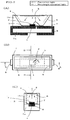
- Fig. 1 shows a known light-emitting apparatus that uses a wavelength conversion material.
- This light-emitting apparatus can include an insulating base 10, a semiconductor light-emitting device 12, and a light transmitting substrate 16 which is arranged on the insulating base 10.
- a pair of lead electrodes 11 can be formed on the surface of a substrate under the insulating base 10.
- the insulating base 10 can also have a concave portion 13 and a curved portion 14.
- the semiconductor light-emitting device 12 can be placed at the center of the bottom of the concave portion 13.
- the curved portion 14 can be continuous to the periphery of the concave portion 13.
- the semiconductor light-emitting device 12 placed at the center of the bottom of the concave portion 13 can be electrically connected with the pair of lead electrodes 11.
- a wavelength conversion layer 15 can be formed on a surface of the light transmitting substrate 16 where it faces the base 10.
- a reflecting film 17 made of Ag or the like can be formed on the inside of the concave portion 13 and the surface of the curved portion 14.
- the wavelength conversion layer 15 can be made of a resin in which phosphor materials are dispersed. The phosphor materials can be configured/selected for emitting light when excited by excitation light emitted from the semiconductor light-emitting device 12.
- the wavelength conversion layer 15 can be formed on the light transmitting substrate 16 by such means as screen printing.
- the light transmitting substrate 16 can be placed so that the wavelength conversion layer 15 is opposed to the semiconductor light-emitting device 12 and can be situated substantially directly above the concave portion 13 accommodating the device 12.
- the base 10 having the concave portion 13 and the curved portion 14 can, in conjunction with the light transmitting substrate 16 provided with the wavelength conversion layer 15, define a space which is filled with a translucent sealing material 18 to seal the semiconductor light-emitting device 12 and the wavelength conversion layer 15.
- the reflecting film 17 on the curved portion 14 may be coated with a second wavelength conversion layer 19 (for example, see Japanese Unexamined Patent Application Publication No. 2004-56075 A or its corresponding U.S. Patent No. 6,809,342 ).
- the concave portion 13 for accommodating the semiconductor light-emitting device and the curved portion 14 can and often should be formed for the sake of improved light emission efficiency.
- the light-emitting apparatus of this configuration is applied in a white chip LED (a surface mountable LED device emitting light in the white wavelength range) or the like for use in a liquid crystal display backlight of a cellular phone or mobile information terminal.
- the mold for forming the base 10 having the concave portion 13 and the curved portion 14 can and often should have a high degree of precision, and thus may require extremely high skill for fabrication. As a result, there have been problems relating to increased costs for the white chip LED, difficulty in manufacturing, etc.
- the light-emitting apparatus can develop unevenness in color inside.
- a reason for this is as follows: When the light-emitting apparatus is viewed from its optical axis, the color of the excitation light is dominant in an area immediately near the semiconductor light-emitting device 12. Meanwhile, the color complementary to that of the excitation light, occurring from the wavelength conversion layer, is dominant in surrounding areas somewhat away from the area immediately near the semiconductor light-emitting device 12. In terms of intensity (intensity distribution), there have been problems in that the intensity peaks at the area immediately near the semiconductor light-emitting device 12 and it decreases toward the periphery.
- the base 10 is provided with the concave portion 13 alone without the curved portion 14, and only the second wavelength conversion layer 19 is formed on the inside of the concave portion 13 without the first wavelength conversion layer 15.
- the light of the semiconductor light-emitting device 12 has difficulty in reaching the second wavelength conversion layer 19. Consequently, the complementary color of the excitation light, i.e., the light from the wavelength conversion layer 19 is dominant in the area immediately near the wavelength conversion layer 19 while the color of the light emitted from the semiconductor light-emitting device 12 is dominant in the other areas. That is, unevenness in color has also occurred in this case.
- intensity distribution there have also been problems similar to the intensity problems described above.
- WO 03/107441 A discloses an emitter package exhibiting limited wavelength variations between batches and consistent wavelength and emission characteristics with operation.
- the emitter package comprises a semiconductor emitter and a conversion material.
- the conversion material is arranged to absorb substantially all of the light emitting from the semiconductor emitter and re-emit light at one or more different wavelength spectrums of light.
- the conversion material is also arranged so that there is not an excess of conversion material to block said re-emitted light as it emits from said emitter package, said emitter package emitting light at said one or more wavelength spectrums from said conversion material.
- the semiconductor emitter is preferably a light emitting diode (LED) or laser diode.
- US 2003/0132701 A1 discloses a light emitting apparatus provided with a fluorescent substance sealed within a cured epoxy resin. More particularly, in a light emitting apparatus comprising a light emitting device, a fluorescent substance is provided which is capable of absorbing at least a portion of light emitted by the light emitting device and emitting light having a different wavelength, and a color converting member which contains the fluorescent substance and directly coat the light emitting device, the color converting member contains at least an epoxy resin derived from triazine and a mixing ratio of the epoxy resin derived from triazine to the acid anhydride curing agent in the color converting member is from 100:80 to 100:240.
- a mixing ratio of the epoxy resin derived from triazine to the acid anhydride curing agent in the color converting member is from 100:80 to 100:240.
- EP-A-1 107 321 discloses a light emitting diode comprising a light emitting diode element mounted on a glass epoxy substrate. The light emitting diode element is protected at its surface side by a resin seal member.
- a light emitting diode element for blue luminescence, formed of gallium nitride type compound semiconductor is used as the above-mentioned light emitting diode element; and a fluorescent material containing layer composed of a fluorescent material dispersed into an adhesive is arranged on the back side of this light emitting diode element. On the back side of the light emitting diode element, blue luminescence is converted in wavelength to produce white luminescence of high intensity.
- WO 03/034508 A discloses a light emitting device comprising a luminescent element and coating layers including a phosphor and provided in contact with each other. More particularly, a light emitting device comprises a luminescent element placed on a support and coating layers which bind a phosphor for absorbing a light from the luminescent element and converting the wave length thereof to the surface of the luminescent element, wherein the coating layers comprise an inorganic material comprising an oxide and a hydroxide of at least one element selected from the group consisting of Si, Al, Ga, Ti, Ge, P, B, Zr, Y, Sn, Pb and alkaline earth metals the light emitting device wherein the adhesive comprises the same inorganic material as that for the coating layers. Accordingly, there are no wavelength conversion layers separately formed on a bottom of a concave and in an opening thereof with a distance there between like the present invention.
- a semiconductor light-emitting apparatus is provided as forth in claim 1.
- the excitation light that is emitted in every direction from the semiconductor light-emitting device can generally undergo sufficient wavelength conversion before being emitted out of the light-emitting apparatus. This means a significant improvement to reducing color unevenness and intensity unevenness.
- the configuration capable of reducing intensity unevenness and suppressing the transmission of the near-ultraviolet light can prevent a light guide plate and the like from ultraviolet degradation.
- constituent light sources of white light such as blue light, are used as the excitation light source, it is possible to fabricate a white LED of reduced color unevenness and intensity unevenness.
- Fig. 1 is a schematic diagram showing a semiconductor light-emitting apparatus according to a known packaging technique
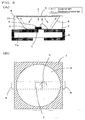
- Figs. 2A-2C are schematic diagrams showing an embodiment of a semiconductor light-emitting apparatus made in accordance with the principles of the present invention, where Fig. 2A is a sectional view taken along the line IIA-IIA of Fig. 2B, Fig. 2B is a schematic plan view, and Fig. 2C is a sectional view taken along the line IIC-IIC of Fig. 2B ;
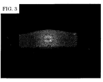
- Fig. 3 is a diagram showing the intensity distribution of a comparative example of the semiconductor light-emitting apparatus of Figs. 2A-2C ;
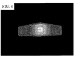
- Fig. 4 is a diagram showing the intensity distribution of a particular fabrication of the semiconductor light-emitting apparatus of Figs. 2A-2C ;
- FIGs. 5A and 5B are schematic diagrams showing another embodiment of a semiconductor light-emitting apparatus made in accordance with the principles of the invention, where Fig. 5A is a sectional view of the same, and Fig. 5B is a plan view of the same;
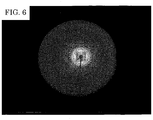
- Fig. 6 is a diagram showing the intensity distribution of a comparative example of the semiconductor light-emitting apparatus of Figs. 5A-B ;
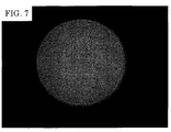
- Fig. 7 is a diagram showing the intensity distribution of a particular fabrication of the semiconductor light-emitting apparatus of Figs. 5A-B ;
- Fig. 8 is a chart showing the emission spectra of the light emitted from a particular fabrication of a semiconductor light-emitting apparatus of Figs. 5A-B as compared to a comparative semiconductor light-emitting apparatus.
- Figs. 2A-2C are explanatory diagrams showing an embodiment of the semiconductor light-emitting apparatus made in accordance with the principles of the invention.
- Fig. 2A is a sectional view taken along the line IIA-IIA of Fig. 2B.
- Fig. 2B is a schematic plan view.
- Fig. 2C is a sectional view taken along the line IIC-IIC of Fig. 2B .
- the semiconductor light-emitting apparatus of Fig. 2A can include an insulating base 7, a semiconductor light-emitting device 1, and a wavelength conversion portion.
- the insulating base 7 can also include a concave portion 6.
- the semiconductor light-emitting device 1 can be arranged at the bottom of the concave portion 6.
- the wavelength conversion portion can be composed of a first wavelength conversion layer 3 formed on the bottom of the concave portion 6, and a second wavelength conversion layer 5 formed in the opening of the concave portion 6 at a distance above the semiconductor light-emitting device 1.
- the space defined by the concave portion 6 of the base 7 and the second wavelength conversion layer 5 can be filled with a sealing material 4 for transmitting light emitted from the semiconductor light-emitting device 1.
- the base 7 can include and/or consist of a substrate part 7a and a reflecting frame part 7b.
- the substrate part 7a can be provided with at least a pair of lead electrodes 8, or an anode electrode and a cathode electrode.
- the lead electrodes 8 can project out of the base 7.
- the reflecting frame part 7b can be arranged on the substrate part 7a and can have the concave portion 6 in its center.
- the pair of lead electrodes 8 can be formed so that the electrodes 8 are exposed in the bottom area of the concave portion 6.
- the semiconductor light-emitting device is surrounded by the reflecting frame part 7b, and the concave portion 6 is formed in the center of the same.
- the reflecting frame part 7b may be formed in other manners, including on either one of the pairs of opposed sides and not on the other.
- the reflecting frame part 7b can be formed on the right and left alone, and not on the top and bottom.
- the concave portion 6 can be formed in the middle.
- Examples of the methods for forming the concave portion 6 into which the semiconductor light-emitting device 1 can be arranged and fixed are, though not restrictive, described as follows.
- Integral molding methods can be used such that the electrodes 8 are loaded as insert members into a mold, and the material is injected into the mold so that the base 7 (the substrate part 7a and the reflecting frame part 7b) is insert-molded.
- Bonding-after methods can be used such that the electrodes 8 are fixed to the surface of the substrate part 7a before the reflecting frame part 7b is attached to form the base 7.
- the material(s) for making the base 7 can be selected from among ones that develop no electric short circuit between the anode and cathode electrodes, or the lead electrodes 8.
- the substrate part 7a can be made of an insulating material such as insulating resins including a glass fiber containing epoxy resin, and ceramics. In a practical viewpoint, it is sometimes preferable to use materials having relatively high melting points so that no deformation occurs at temperatures expected at the time of packaging with solder materials.
- the reflecting frame part 7b can be made of an insulating material having heat resistance to soldering temperatures (around 200°C or below), such as high melting point insulating resins made of liquid polymers including liquid crystal polyester, and ceramics.
- the concave portion 6 may also be preferable for the concave portion 6 to be formed in the center, and that the material be white or the like in color, having a certain degree of high reflectivity.
- the substrate part 7a and the reflecting frame part 7b can be made of liquid crystal polymers. White liquid crystal polymer materials are sometimes superior in many respects, including insulation performance, heat resistance, high reflectivity, and formability.
- a layer of high reflectivity material may be formed on the inside 71 of the concave portion 6 of the base 7 by such means as coating, plating, vapor deposition, and the like.
- the concave portion 6 may be shaped generally like a truncated cone, a truncated pyramid, partially hemispherical surface, etc.
- the concave portion 6 can also have an inclined inner periphery.
- the inner periphery may be shaped generally perpendicular for the sake of a desired reduction in device profile.
- the reflecting frame part 7b can be generally rectangular in the angle of the inner periphery without departing from the spirit and scope of the invention.
- the semiconductor light-emitting device 1 can be attached to the bottom of the concave portion 6.
- the semiconductor light-emitting device 1 is electrically and mechanically fixed onto one of the electrodes 8 by die bonding using an Ag paste.
- a conductive wire 2 that extends from the top of the semiconductor light-emitting device and the other electrode 8 can be connected by wire bonding.
- the semiconductor light-emitting device 1 may be made of any semiconductor material, and preferably of a material that emits light having energy capable of exciting the wavelength conversion material. Semiconductor materials for emitting light in the range of ultraviolet light and blue light are preferable in particular instances. It is also sometimes preferable that the semiconductor light-emitting device 1 fall within the range of 300 and 490 nm in the light emission peak wavelength.
- Examples of the semiconductor materials for making the semiconductor light-emitting device 1 include light-emitting diodes (LEDs) such as group-III nitride compound (for example, In-Ga-Al-N compound) semiconductors, zinc oxide compound (for example, Zn-Mg-O compound) semiconductors, zinc selenide compound (for example, Zn-Mg-Se-S-Te compound) semiconductors, and silicon carbide compound (for example, Si-Ge-C) semiconductors.
- LEDs light-emitting diodes
- group-III nitride compound for example, In-Ga-Al-N compound
- zinc oxide compound for example, Zn-Mg-O compound
- zinc selenide compound for example, Zn-Mg-Se-S-Te compound
- silicon carbide compound for example, Si-Ge-C semiconductors.
- the semiconductor materials are not limited thereto. It is only preferable in certain circumstances that they emit light within the foregoing range of light emission peak wavelengths.
- Figs. 2A-2C deals with the case where the bottom side of the semiconductor light-emitting device 1 establishes electric connection with one of the electrodes 8, and the top side establishes electric connection with the other electrode 8. It is also possible, however, to use a semiconductor device that can establish electric connection with both the electrodes 8 at an identical side, or to different combinations of side, bottom or top mount electrodes.
- the semiconductor light-emitting device can be mechanically bonded onto the substrate part 7a with an adhesive such as an epoxy resin.
- the anode and cathode electrodes formed on the top side of the semiconductor light-emitting device can be electrically bonded to the respective corresponding lead electrodes 8 in pair by conductive wires 2.
- the anode and cathode electrodes of the semiconductor light-emitting device 1 are electrically connected to the corresponding lead electrodes 8 and the device is fixed to the base 7 at the same time by such means as Au-Sn or other eutectic materials, Au bumps, anisotropic conductive sheets, and conductive resins typified by an Ag paste; and those in which either one of the electrodes of the device is electrically connected to the corresponding lead electrode 8 and fixed to the base 7 by using the foregoing materials while the other electrode and the corresponding lead electrode 8 are electrically bonded by a conductive wire.
- the base 7 may be made of metal or other conductive materials.
- the base 7 may also function as one of the lead electrodes 8.
- the base 7, the semiconductor light-emitting device 1, and the lead electrodes 8 There are various forms available for the base 7, the semiconductor light-emitting device 1, and the lead electrodes 8. Regardless of the form that is used, the semiconductor light-emitting device 1 can be fixed onto the base 7, and the anode and cathode lead electrodes 8 can be electrically connected to the corresponding anode and cathode electrodes of the semiconductor light-emitting device 1.
- the first wavelength conversion layer 3 can be formed in the bottom area of the concave portion 6. In the example shown in Figs. 2A-2C , the first wavelength conversion layer 3 is formed on the top area of the substrate part 7a and on the semiconductor light-emitting device 1 at the bottom of the concave portion 6.
- the first wavelength conversion layer 3 can have one or more layers of wavelength conversion materials within a thickness smaller than the height of the semiconductor light-emitting device 1. The ideal thickness depends on various properties, including the wavelength conversion efficiencies of various wavelength conversion materials. In a practical viewpoint, the wavelength conversion layer can have a thickness around 20 to 200 ⁇ m since the semiconductor light-emitting device generally has a thickness of 300 ⁇ m or so.
- the "wavelength conversion portion (or layer)" will refer not only to the layer made of wavelength conversion material alone, but also to the entire area where wavelength conversion material concentrates densely.
- the wavelength conversion layer can refer to an entire area of the sealing portion 4 to be described later where the phosphor particles are distributed densely.
- the first wavelength conversion layer 3 may be formed by any of the following methods: (1) placing the semiconductor light-emitting device 1 on the bottom of the concave portion 6, and then applying a wavelength conversion material such as an inorganic phosphor directly to the bottom of the concave portion 6 to form the first wavelength conversion layer 3; (2) mixing the wavelength conversion material for forming the first wavelength conversion layer 3 into the material for forming the sealing portion 4, injecting the mixed material into the concave portion 6, and hardening the sealing portion 4 when the wavelength conversion material in the mixed material settles out to the bottom area of the concave portion 6 by its own weight and lies densely in this area, so that this area creates the first wavelength conversion layer 3; and (3) attaching, onto the bottom of the concave portion 6a, a wavelength-conversion-material-containing sheet that has a predetermined thickness and a wavelength conversion material at a predetermined density.
- a wavelength conversion material such as an inorganic phosphor
- the first wavelength conversion layer 3 can also be formed on the top of the semiconductor light-emitting device 1.
- the semiconductor light-emitting apparatus can be improved by providing a more even intensity distribution due to the excitation light being emitted directly upward from the semiconductor light-emitting device 1. This configuration allows light to be wavelength converted and scattered as well.
- the first wavelength conversion layer 3 has approximately the same thickness throughout the layer.
- distribution of phosphors that form the first wavelength conversion layer 3 is not limited thereto, and can include various thickness layers and layers that have changing thicknesses.
- the sealing portion 4 can be made of a light transmitting material which maintains the distance from the semiconductor light-emitting device 1 and the first wavelength conversion layer 3 to the second wavelength conversion layer 5.
- the material may also be capable of transmitting both the excitation light from the semiconductor light-emitting device 1 and the wavelength conversion light converted by the wavelength conversion material.
- Some examples include thermosetting resins and low melting point glass.
- the sealing portion 4 may be formed to be hollow (or sealed with a gaseous material) when accompanied with a configuration that fixes the sheet to the reflecting frame part 7b.
- Examples of materials that can be used for making the sealing portion 4 are the following: materials that have a high transmittance up to shortwave regions covering the peak wavelength of light emission from the semiconductor light-emitting device 1; materials that have a constituent material of the first wavelength conversion layer 3 that can be mixed and dispersed therein; and materials in which the constituent material of the first wavelength conversion layer 3 can settle out (be distributed) densely at the bottom of the concave portion 6 when heated and left standing, etc.
- Specific examples include thermosetting resins containing at least one resin selected from the group consisting of epoxy resins, silicone resins, polydimethylsiloxane derivatives having epoxy groups, oxetane resins, acryl resins, and cycloolefin resins.
- epoxy resins made of epoxy resin materials containing hydrogenated bisphenol A diglycidyl ether, alycyclic epoxy carboxylate, and organic sulfonium-hexafluoroantimonate can be used.
- the sealing portion 4 can be shaped so that its top surface that corresponds to a position substantially directly above the semiconductor light-emitting device 1 sinks into a generally recessed surface. This can facilitate the formation of the second wavelength conversion layer 5.
- the second wavelength conversion layer 5 can efficiently scatter the excitation light and the once-wavelength-converted light which is wavelength-converted by the first wavelength conversion layer 3.
- Examples of methods that can be used to form a generally recessed surface on the sealing portion 4 are as follows: heating the material of the sealing portion 4 for hardening, at which time the surface is formed naturally through solvent evaporation; controlling the composition of the material of the sealing portion 4 and the amount of injection of the same to cause a meniscus phenomenon, and harden it in that state to form the recessed surface; and forming the recessed surface by compression molding or the like.
- the second wavelength conversion layer 5 can be arranged at an appropriate distance from the semiconductor light-emitting device 1 and the first wavelength conversion layer 3 so that it covers the vicinity of the opening end of the concave portion 6 (see Fig. 2A ), at least over the semiconductor light-emitting device 1 in plan view.
- the second wavelength conversion layer 5 is arranged at the center of the opening of the concave portion 6 and has an area narrower than the opening.
- the second wavelength conversion layer 5 is formed to cover the entire opening of the concave portion 6.
- the second wavelength conversion layer 5 can be formed by mixing an appropriate binder resin and a wavelength conversion material, and arranging this mixed material onto the sealing portion 4 directly above the semiconductor light-emitting device 1 by such means as potting using a dispenser.
- the sealing portion 4 can be shaped so that its top sinks into a generally curved surface.
- the recess formed in the top of the sealing portion 4 can be filled with the constituent material of the second wavelength conversion layer 5 to form the second wavelength conversion layer 5.
- the binder resin of the second wavelength conversion layer 5 may be the same material as the constituent material of the sealing portion 4. Any material may be used and preferably has excellent adhesiveness with the sealing portion 4 and causes little or no degradation due to the excitation light.
- the thickness of the second wavelength conversion layer 5 even a single layer of particles of the wavelength conversion material is effective. Since excessive thicknesses can lower the output efficiency, a thickness in the range of 20 ⁇ m to 150 ⁇ m may be desirable in some circumstances. A thickness that is smaller than that of the first wavelength conversion layer 3 is also often preferable.
- the wavelength conversion materials for forming the first wavelength conversion layer 3 and the second wavelength conversion layer 5 convert the peak wavelength of light emission from the semiconductor light-emitting device 1 into longer peak wavelengths of light emission.
- the wavelength conversion materials may contain one or more types of materials. In consideration of color unevenness, the first wavelength conversion layer 3 and the second wavelength conversion layer 5 can be made of the same wavelength conversion material. Nevertheless, the first wavelength conversion layer 3 and the second wavelength conversion layer 5 may be made of respective different wavelength conversion materials, depending on the physical properties of the constituent materials, such as reflectance. Examples of wavelength conversion materials include the following.
- a 3 B 5 O 12 :M phosphors (A: at least one element selected from among Y, Gd, Lu, and Tb; B: at least one element selected from A1 and Ga; and M: at least one ion selected from among Ce 3+ , Tb 3+ , Eu 3+ , Cr 3+ , Nd 3+ , and Er 3+ ); rare-earth doped barium-aluminum-magnesium compound phosphors (BAM phosphors); sulfide compound phosphors typified by Y 2 O 2 S:Eu 3+ and ZnS:Cu,Al; rare-earth doped thiogallate phosphors such as (Sr,Ca)S:Eu 2+ , CaGa 2 S 4 :Eu 2+ , and SrGa 2 S 4 :Eu 2+ ; and phosphors containing at least one of aluminate compositions such as TbAlO 3 :Ce 3+ .
- the wavelength conversion layers may include scattering agents such as barium sulfate, magnesium oxide, and/or silicon oxide for the sake of assisting the reflection of the excitation light and the wavelength conversion light.
- the excitation light can undergo the same wavelength conversion, reflection, etc. as in the foregoing case where the excitation light constitutes a light source of white light.
- the light can be emitted from the opening of the concave portion 6.
- the excitation light is in the ultraviolet or near-ultraviolet region, however, the external emission of the excitation light can cause the ultraviolet degradation of electronic parts such as a light guide plate. It may therefore be preferable to prevent the excitation light from being emitted outside of the light-emitting apparatus as much as possible.
- the thicknesses and constituent materials of the first wavelength conversion layer 3 and the second wavelength conversion layer 5 be adjusted to reduce ultraviolet rays to be emitted outside.
- the external emission of the ultraviolet rays can also be reduced by configuring the semiconductor light-emitting apparatus so that the light emitted from the semiconductor light-emitting device always takes the path through the first wavelength conversion layer 3 and/or the second wavelength conversion layer 5.
- the second wavelength conversion layer 5 is arranged to cover the entire opening of the concave portion 6 so that all the emitted light can be turned into wavelength conversion light.
- a semiconductor light-emitting apparatus having an oblong rectangular shape in plan view as shown in Figs. 2A and 2B was fabricated.
- a description of this specific fabrication is now provided as an example of an apparatus and method that corresponds to the embodiment shown in Figs. 2A-C .
- a white thermosetting resin having a high melting point was insert molded with Ag-plated lead electrodes 8 as the insert members.
- a base 7 having a concave portion 6 and integrated electrodes 8 was fabricated.
- IIC-IIC shown in Fig.
- the concave portion 6 was formed so that the top surfaces of the lead electrodes 8 and the inside of the concave portion 6 of the reflecting frame part 7b formed an angle of approximately 90°. Furthermore, in the section taken along the line IIA-IIA of Fig. 2A , the concave portion 6 was formed so that the top surfaces of the lead electrodes 8 and the inside of the concave portion 6 of the reflecting frame part 7b formed an obtuse angle.
- a semiconductor device for emitting blue light made of an InGaN compound semiconductor (having a light emission peak wavelength of 470 nm) formed on an n-type SiC substrate, was used.
- a cathode electrode formed on this n-type substrate and its corresponding lead electrode 8 were electrically bonded to each other and mechanically fixed to the base 7 with an Ag paste.
- an epoxy resin was mixed with an appropriate amount of YAG phosphor to form the constituent material.
- YAG phosphors generate wavelength conversion light of yellow when excited by blue light of near 470 nm.
- This constituent material was filled into the concave portion 6, and left standing so that the phosphor naturally settled out to the bottom area of the concave portion 6. Then, under the condition of 150°C and after hour, the material was hardened to simultaneously form the first wavelength conversion layer 3 and the sealing portion 4.
- the constituent material of the second wavelength conversion layer 5 i.e., a mixed material of epoxy resin and the previously described phosphor, was applied to a recess in the top of the sealing portion 4 which had been generated by itself during the hardening of the epoxy resin.
- the resultant mixture was hardened at 150°C for one hour, to form the second wavelength conversion layer 5.
- Fig. 4 shows the intensity distribution of the semiconductor light-emitting apparatus, as viewed from its optical axis, when the semiconductor light-emitting device as described in the above fabrication description was energized and lit by a current of 1 mA.
- white areas have higher intensities, and black areas lower intensities.
- a semiconductor light-emitting apparatus having the same oblong rectangular shape was fabricated under the same condition as in the above described configuration/fabrication of the embodiment of Figs. 2A-C .
- the first wavelength conversion layer 3 and the sealing portion 4 were formed under the same conditions, whereas the second wavelength conversion layer 5 was not formed.
- Fig. 3 shows the intensity distribution of the semiconductor light-emitting apparatus, as viewed from its optical axis, when the semiconductor light-emitting device of the comparative example (without the second wavelength conversion layer 5) was energized and lit by the same current of 1 mA. Again, in Fig. 3 , white areas have higher intensities, and black areas lower intensities.
- the semiconductor light-emitting apparatus used to create the light intensity distribution of Fig. 4 showed more uniform white light emission over almost all areas, with no noticeable unevenness in intensity distribution as compared to that of Fig. 3 .
- FIG. 5A and 5B A description of this specific fabrication (fabrication II) is now provided as an example of an apparatus and method that corresponds to the embodiment shown in Figs. 5A-B .
- a white thermosetting resin having a high melting point was insert molded with Ag-plated lead electrodes 8 as the insert members.
- a base 7 having a concave portion 6 and integrated electrodes 8 was fabricated.
- the concave portion 6 was shaped like a bowl so that the top surfaces of the lead electrodes 8 and the inside of the concave portion 6 of the reflecting frame part 7b formed an angle of approximately 50°.
- a semiconductor device for emitting ultraviolet rays made of an InGaN compound semiconductor (having a light emission peak wavelength of 395 nm) formed on an n-type SiC substrate, was used.
- a cathode electrode formed on this n-type substrate and its corresponding lead electrode 8 were electrically bonded to each other and mechanically fixed to the base 7 with an Ag paste.
- predetermined proportions of blue, red, and green light emission phosphors, or a barium-aluminum-magnesium compound phosphor (BAM phosphor), Y 2 O 2 S:Eu 3+ , and ZnS:Cu,Al, respectively, were mixed to form a wavelength conversion material.
- the thus obtained mixed phosphors were mixed and dispersed into an epoxy resin at a rate of 20% by weight.
- the employed epoxy resin contained a certain amount of UV absorbents. Alternatively, it can be noted that resin having high UV resistance by itself may have been used.
- the resulting constituent material was filled into the concave portion 6, and left standing so that the phosphors naturally settled out to the bottom area of the concave portion 6. Then, under the condition of 150°C and after 1 hour, the material was hardened to simultaneously form the first wavelength conversion layer 3 and the sealing portion 4.
- the constituent material of the second wavelength conversion layer 5 i.e., the mixed material that included epoxy resin and 20% by weight of the foregoing described mixed phosphors, was applied to a recess in the top of the sealing portion 4 which had been generated by itself during the hardening of the epoxy resin.
- the resultant material was hardened at 150°C for one hour to form the second wavelength conversion layer 5.
- the second wavelength conversion layer 5 was formed only in the center area of the opening of the concave portion 6, not in the surrounding areas.
- the second wavelength conversion layer 5 was formed over the entire opening of the concave portion 6 as shown in Figs. 5A and 5B .
- the first wavelength conversion layer 3 and the second wavelength conversion layer 5 both had a thickness of approximately 130 ⁇ m.
- Fig. 7 shows the intensity distribution of the semiconductor light-emitting apparatus, as viewed from its optical axis, when the above-described fabrication II of the semiconductor light-emitting device was energized and lit by a current of 1 mA.
- white areas have higher intensities, and black areas lower intensities.
- a semiconductor light-emitting apparatus having the same square shape was fabricated under the same conditions as in fabrication II.
- the first wavelength conversion layer 3 and the sealing portion 4 were formed under the same conditions, whereas the second wavelength conversion layer 5 was not formed.
- Fig. 6 shows the intensity distribution of the semiconductor light-emitting apparatus, as viewed from its optical axis, when the semiconductor light-emitting device of the comparative example to fabrication II was energized and lit by the same current of 1 mA as was used with fabrication II. Again, in Fig. 6 , white areas have higher intensities, and black areas lower intensities.
- a spectral analysis was conducted on the light emitted from the semiconductor light-emitting apparatuses of the fabrication II device and the comparative example to fabrication II device.
- Fig. 8 shows the results.
- the semiconductor light-emitting apparatuses were installed in the integrating sphere of a spectroscopic analyzer, energized by a current of 20 mA, and measured for the light emitted at that time.
- the light emitted from the semiconductor light-emitting apparatus according to fabrication II contains 50% or less excitation light, i.e., light having a peak wavelength of 395 nm, as compared to the comparative example to fabrication II described above where the second wavelength conversion layer is not formed.
Landscapes
- Led Device Packages (AREA)
- Luminescent Compositions (AREA)
Claims (9)
- Halbleiterleuchtvorrichtung, die Folgendes aufweist:eine Basis (7) mit einem konkaven Teil (6) mit einem Boden und einer Öffnung;ein Paar von Elektroden (8), das an dem Boden des konkaven Teils (6) angeordnet ist;eine Halbleiterleuchtvorrichtung (1), die an dem Boden des konkaven Teils (6) angeordnet ist und elektrisch mit dem Paar von Elektroden (8) verbunden ist;einen Wellenlängenumwandlungsteil (3, 5), der imstande ist, die Wellenlänge des Lichts zu verändern, das von der Halbleiterleuchtvorrichtung (1) emittiert wird, wobei der Wellenlängenumwandlungsteil (3, 5) eine erste Wellenlängenumwandlungsschicht (3), die an dem Boden des konkaven Teils (6) undauf der Halbleiterleuchtvorrichtung (1) gebildet ist, und eine zweite Wellenlängenumwandlungsschicht (5) umfasst, die in der Öffnung des konkaven Teils (6) und in einer Entfernung oberhalb der Halbleiterleuchtvorrichtung (1) gebildet ist; undeinen Raum, der durch die Basis (7) und die zweite Wellenlängenumwandlungsschicht (5) definiert wird, wobei der Raum mit einem Abdichtungsteil (4) vorgesehen ist, der ein Material enthält, das imstande ist, im Wesentlichen das Licht, das von der Halbleiterleuchtvorrichtung (1) emittiert wird, und das Wellenlängenumwandlungslicht zu übertragen, das von den ersten und zweiten Wellenlängenumwandlungsschichten (3, 5) emittiert wird,dadurch gekennzeichnet, dassdie zweite Wellenlängenumwandlungsschicht (5) in einer Entfernung oberhalb der ersten Wellenlängenumwandlungsschicht (3) gebildet ist;eine obere Oberfläche des Abdichtungsteils (4), der direkt oberhalb der Halbleiterieuchtvorrichtung (1) gelegen ist, eine ausgenommene, gekrümmte Oberfläche aufweist, die zu der Halbleiterleuchtvorrichtung (1) hin ausgenommen ist; undeine Dicke der zweiten Wellenlängenumwandlungsschicht (5) kleiner als die der ersten Wellenlängenumwandlungsschicht (3) ist.
- Halbleiterleuchtvorrichtung gemäß Anspruch 1, dadurch gekennzeichnet, dass die erste Wellenlängenumwandlungsschicht (3) und/oder die zweiten Wellenlängenumwandlungsschicht (5) zumindest eine Art von Phosphor umfasst, der aus der Gruppe ausgewählt wird, die aus Folgendem besteht: Phosphore mit der Zusammensetzung aus A3B5O12:M, wobei A zumindest ein Element umfasst, das aus Y, Gd, Lu und Tb ausgewählt wird, B zumindest ein Element umfasst, das aus Al und Ga ausgewählt wird, und M zumindest ein Ion umfasst, dass aus Ce3+, Tb3+, Eu3+, Cr3+, ND3+ und Er3+ ausgewählt wird; Seltenerddotierte Barium-Aluminium-Magnesium-Verbindungsphosphore; Sulfidverbindungsphosphore; Seltenerddotierte Thiogallatphosphore und Aluminatphosphore.
- Halbleiterleuchtvorrichtung gemäß Anspruch 1, die dadurch gekennzeichnet ist, dass das Material des Dichtungsteils (4) zumindest ein Harz umfasst, das aus der Gruppe ausgewählt wird, die aus Epoxidharzen, Silikonharzen, Polydimethylsiloxanderivaten mit Epoxygruppen, Oxetanharzen, Acrylharzen und Cycloolefinharzen besteht.
- Halbleiterleuchtvorrichtung gemäß Anspruch 1, die dadurch gekennzeichnet ist, dass die zweite Wellenlängenumwandlungsschicht (5) gebildet ist, um die gesamte Öffnung des konkaven Teils (6) abzudecken.
- Halbleiterleuchtvorrichtung gemäß Anspruch 1, die dadurch gekennzeichnet ist, dass der konkave Teil (6) als ein Kegelstumpf gebildet ist
- Halbleiterleuchtvorrichtung gemäß Anspruch 1, die dadurch gekennzeichnet ist, dass der konkave Teil (6) entweder als eine invertierte Pyramide, ein Rechteckfeld oder als ein Teil einer Halbkugel gebildet ist.
- Halbleiterleuchtvorrichtung gemäß Anspruch 1, die dadurch gekennzeichnet ist, dass das Wellenlängenumwandlungsmaterial an einem Teil nahe des Bodens des konkaven Teils (6) dichter verglichen mit einer Stelle ist, die von dem Boden des konkaven Teils (6) beabstandet ist.
- Halbleiterleuchtvorrichtung gemäß Anspruch 1, die dadurch gekennzeichnet ist, dass die zweite Wellenlängenumwandlungsschicht (5) an der Mitte der Öffnung des konkaven Teils (6) angeordnet ist, und einen Bereich besitzt, der enger als die Öffnung ist.
- Verfahren zur Herstellung einer Halbleiterleuchtvorrichtung, wobei das Verfahren die folgenden Schritte aufweist:Vorsehen einer Basis (7), die einen konkaven Teil (6) mit einem Boden besitzt, eines Paars von Elektroden (8), einer Halbleiterleuchtvorrichtung (1), die an dem Boden des konkaven Teils (6) gelegen und elektrisch mit dem Paar von Elektroden (8) verbunden ist, eines Wellenlängenumwandlungsteils (3, 5), der konfiguriert ist, um die Wellenlänge des Lichts zu verändern, das von der Halbleiterleuchtvorrichtung (1) emittiert wird, und eines Abdichtungsteils (4);Laden der Halbleiterleuchtvorrichtung (1) auf den konkaven Teil (6) der Basis (7), so dass diese elektrisch mit dem Paar von Elektroden (8) verbunden werden kann;Einspritzen eines Mischmaterials in den konkaven Teil (6), wobei das Mischmaterial ein Harz zum Bilden eines Abdichtungsteils (4) und ein Wellenlängenumwandlungsmaterial zum Bilden des Wellenlängenumwandlungsteils (3) aufweist, wobei das Wellenlängenumwandlungsmaterial zumindest eine Art von Phosphor aufweist, der aus der Gruppe ausgewählt wird, die aus Folgendem besteht: Phosphore mit der Zusammensetzung aus A3B5O12:M), wobei A zumindest ein Element umfasst, das aus Y, Gd, Lu und Tb ausgewählt wird, B zumindest ein Element umfasst, das aus Al und Ga ausgewählt wird, und M zumindest ein Ion umfasst, dass aus Ce3+, Tb3+, Eu3+, Cr3+, ND3+ und Er3+ ausgewählt wird; Seltenerddotierte Barium-Aluminium-Magnesium-Verbindungsphosphore; Sulfidverbindungsphosphore; Seltenerddotierte Thiogallatphosphore und Aluminatphosphore;Stehenlassen des Mischmaterials, so dass sich das Wellenlängenumwandlungsmaterial in einem Bodenbereich des konkaven Teils (6) absetzt, um eine erste Wellenlängenumwandlungsschicht (3) zu bilden, wobei die Wellenlängenumwandlungsschicht konfiguriert ist, um als Wellenlängenumwandlungsteil (3) zu dienen;Aushärten des Mischmaterials in dem konkaven Teil (6), wobei die erste Wellenlängenumwandlungsschicht (3) und der Abdichtungsteil (4) simultan gebildet werden;Bilden einer Ausnehmung an der Oberseite des Abdichtungsteils (4) durch Kompressionsformen; undBilden einer zweiten Wellenlängenumwandlungsschicht (5), die konfiguriert ist, um als Wellenlängenumwandlungsteil (5) durch Einkapseln des Mischmaterials zu dienen, um die Ausnehmung auf dem Abdichtungsteil (4) zu füllen.
Applications Claiming Priority (2)
| Application Number | Priority Date | Filing Date | Title |
|---|---|---|---|
| JP2003433351A JP2005191420A (ja) | 2003-12-26 | 2003-12-26 | 波長変換層を有する半導体発光装置およびその製造方法 |
| JP2003433351 | 2003-12-26 |
Publications (3)
| Publication Number | Publication Date |
|---|---|
| EP1548851A2 EP1548851A2 (de) | 2005-06-29 |
| EP1548851A3 EP1548851A3 (de) | 2009-02-18 |
| EP1548851B1 true EP1548851B1 (de) | 2012-02-22 |
Family
ID=34545075
Family Applications (1)
| Application Number | Title | Priority Date | Filing Date |
|---|---|---|---|
| EP04030704A Expired - Lifetime EP1548851B1 (de) | 2003-12-26 | 2004-12-23 | Lichtemittierende Halbleitervorrichtung mit Materialien zur Wellenlängenumwandlung und deren Herstellungsverfahhren |
Country Status (3)
| Country | Link |
|---|---|
| US (1) | US7260123B2 (de) |
| EP (1) | EP1548851B1 (de) |
| JP (1) | JP2005191420A (de) |
Families Citing this family (69)
| Publication number | Priority date | Publication date | Assignee | Title |
|---|---|---|---|---|
| US5778016A (en) | 1994-04-01 | 1998-07-07 | Imra America, Inc. | Scanning temporal ultrafast delay methods and apparatuses therefor |
| DE102004021233A1 (de) * | 2004-04-30 | 2005-12-01 | Osram Opto Semiconductors Gmbh | Leuchtdiodenanordnung |
| WO2006038502A1 (ja) * | 2004-10-01 | 2006-04-13 | Nichia Corporation | 発光装置 |
| KR100593933B1 (ko) * | 2005-03-18 | 2006-06-30 | 삼성전기주식회사 | 산란 영역을 갖는 측면 방출형 발광다이오드 패키지 및이를 포함하는 백라이트 장치 |
| JP2007027431A (ja) | 2005-07-15 | 2007-02-01 | Toshiba Corp | 発光装置 |
| JP2007095807A (ja) | 2005-09-27 | 2007-04-12 | Sanyo Electric Co Ltd | 発光装置及びその製造方法 |
| US20070096139A1 (en) * | 2005-11-02 | 2007-05-03 | 3M Innovative Properties Company | Light emitting diode encapsulation shape control |
| JP4771800B2 (ja) * | 2005-12-02 | 2011-09-14 | スタンレー電気株式会社 | 半導体発光装置及びその製造方法 |
| US8044412B2 (en) | 2006-01-20 | 2011-10-25 | Taiwan Semiconductor Manufacturing Company, Ltd | Package for a light emitting element |
| US8969908B2 (en) * | 2006-04-04 | 2015-03-03 | Cree, Inc. | Uniform emission LED package |
| US9502624B2 (en) * | 2006-05-18 | 2016-11-22 | Nichia Corporation | Resin molding, surface mounted light emitting apparatus and methods for manufacturing the same |
| KR20140146210A (ko) | 2006-06-02 | 2014-12-24 | 히타치가세이가부시끼가이샤 | 광반도체소자 탑재용 패키지 및 이것을 이용한 광반도체장치 |
| US7703945B2 (en) * | 2006-06-27 | 2010-04-27 | Cree, Inc. | Efficient emitting LED package and method for efficiently emitting light |
| US7889421B2 (en) * | 2006-11-17 | 2011-02-15 | Rensselaer Polytechnic Institute | High-power white LEDs and manufacturing method thereof |
| JP2008205170A (ja) * | 2007-02-20 | 2008-09-04 | Nec Lighting Ltd | 発光半導体デバイス |
| WO2008111504A1 (ja) * | 2007-03-12 | 2008-09-18 | Nichia Corporation | 高出力発光装置及びそれに用いるパッケージ |
| JP2010525512A (ja) | 2007-04-17 | 2010-07-22 | コーニンクレッカ フィリップス エレクトロニクス エヌ ヴィ | 照明システム |
| US7942556B2 (en) * | 2007-06-18 | 2011-05-17 | Xicato, Inc. | Solid state illumination device |
| US9401461B2 (en) * | 2007-07-11 | 2016-07-26 | Cree, Inc. | LED chip design for white conversion |
| US10505083B2 (en) * | 2007-07-11 | 2019-12-10 | Cree, Inc. | Coating method utilizing phosphor containment structure and devices fabricated using same |
| KR100882204B1 (ko) * | 2007-08-08 | 2009-02-06 | (주) 아모엘이디 | 반도체 패키지 |
| DE102007057710B4 (de) * | 2007-09-28 | 2024-03-14 | OSRAM Opto Semiconductors Gesellschaft mit beschränkter Haftung | Strahlungsemittierendes Bauelement mit Konversionselement |
| US9086213B2 (en) * | 2007-10-17 | 2015-07-21 | Xicato, Inc. | Illumination device with light emitting diodes |
| JP2009130301A (ja) * | 2007-11-27 | 2009-06-11 | Sharp Corp | 発光素子および発光素子の製造方法 |
| EP2216834B1 (de) | 2007-11-29 | 2017-03-15 | Nichia Corporation | Lichtemittierende vorrichtung |
| RU2508616C2 (ru) * | 2008-02-27 | 2014-02-27 | Конинклейке Филипс Электроникс Н.В. | Осветительное устройство с сид и одним или более пропускающими окнами |
| US8877524B2 (en) * | 2008-03-31 | 2014-11-04 | Cree, Inc. | Emission tuning methods and devices fabricated utilizing methods |
| CN101577298A (zh) * | 2008-05-07 | 2009-11-11 | 富准精密工业(深圳)有限公司 | 发光二极管及其封装方法 |
| JP5363789B2 (ja) * | 2008-11-18 | 2013-12-11 | スタンレー電気株式会社 | 光半導体装置 |
| US8220971B2 (en) | 2008-11-21 | 2012-07-17 | Xicato, Inc. | Light emitting diode module with three part color matching |
| US9631782B2 (en) | 2010-02-04 | 2017-04-25 | Xicato, Inc. | LED-based rectangular illumination device |
| JP5249283B2 (ja) * | 2010-05-10 | 2013-07-31 | デクセリアルズ株式会社 | 緑色発光蛍光体粒子及びその製造方法、並びに、色変換シート、発光装置及び画像表示装置組立体 |
| KR101735670B1 (ko) * | 2010-07-13 | 2017-05-15 | 엘지이노텍 주식회사 | 발광 소자 |
| US20120051045A1 (en) | 2010-08-27 | 2012-03-01 | Xicato, Inc. | Led Based Illumination Module Color Matched To An Arbitrary Light Source |
| TWM401871U (en) * | 2010-09-14 | 2011-04-11 | Hon Hai Prec Ind Co Ltd | Light emitting diode lead frame |
| DE102010063779A1 (de) | 2010-12-21 | 2012-06-21 | Osram Ag | Beleuchtungsanordnung |
| WO2012103919A1 (de) * | 2011-01-31 | 2012-08-09 | Osram Ag | Beleuchtungsvorrichtung mit leuchtstoffelement und optischem system |
| KR20120088130A (ko) * | 2011-01-31 | 2012-08-08 | 서울반도체 주식회사 | 파장변환층을 갖는 발광 소자 및 그것을 제조하는 방법 |
| JP5498417B2 (ja) * | 2011-03-15 | 2014-05-21 | 株式会社東芝 | 半導体発光装置及びその製造方法 |
| US8754440B2 (en) * | 2011-03-22 | 2014-06-17 | Tsmc Solid State Lighting Ltd. | Light-emitting diode (LED) package systems and methods of making the same |
| JP2012216712A (ja) | 2011-03-28 | 2012-11-08 | Nitto Denko Corp | 発光ダイオード装置の製造方法および発光ダイオード素子 |
| JP5666962B2 (ja) | 2011-03-28 | 2015-02-12 | 日東電工株式会社 | 発光ダイオード装置およびその製造方法 |
| DE102012006924A1 (de) * | 2011-04-06 | 2012-10-11 | Tek Beng Low | LED-Beleuchtungsmodul mit gleichförmiger Lichtabgabe |
| JP5700544B2 (ja) | 2011-04-14 | 2015-04-15 | 日東電工株式会社 | 発光ダイオード装置の製造方法 |
| JP5745319B2 (ja) | 2011-04-14 | 2015-07-08 | 日東電工株式会社 | 蛍光反射シート、および、発光ダイオード装置の製造方法 |
| JP5670249B2 (ja) | 2011-04-14 | 2015-02-18 | 日東電工株式会社 | 発光素子転写シートの製造方法、発光装置の製造方法、発光素子転写シートおよび発光装置 |
| JP5840377B2 (ja) | 2011-04-14 | 2016-01-06 | 日東電工株式会社 | 反射樹脂シートおよび発光ダイオード装置の製造方法 |
| US8604684B2 (en) * | 2011-05-16 | 2013-12-10 | Cree, Inc. | UV stable optical element and LED lamp using same |
| JP5772293B2 (ja) * | 2011-06-28 | 2015-09-02 | 日亜化学工業株式会社 | 発光装置及びその製造方法 |
| JP5703997B2 (ja) * | 2011-06-29 | 2015-04-22 | 豊田合成株式会社 | 発光装置 |
| US8558252B2 (en) * | 2011-08-26 | 2013-10-15 | Cree, Inc. | White LEDs with emission wavelength correction |
| JP6382792B2 (ja) * | 2012-03-30 | 2018-08-29 | コーニンクレッカ フィリップス エヌ ヴェKoninklijke Philips N.V. | 発光デバイス及び波長変換材料を含む光学キャビティ |
| WO2013180365A1 (en) * | 2012-05-31 | 2013-12-05 | Lg Innotek Co., Ltd. | Member for cotrolling luminous flux, method for fabricating the member, display device, and light emitting device |
| US20130342103A1 (en) * | 2012-06-25 | 2013-12-26 | Shing-Chung Wang | Solid state lighting luminaire and a fabrication method thereof |
| JP6215525B2 (ja) * | 2012-10-23 | 2017-10-18 | スタンレー電気株式会社 | 半導体発光装置 |
| KR102019499B1 (ko) * | 2012-11-05 | 2019-09-06 | 엘지이노텍 주식회사 | 발광 소자 및 이를 구비한 조명 시스템 |
| CN103855142B (zh) * | 2012-12-04 | 2017-12-29 | 东芝照明技术株式会社 | 发光装置及照明装置 |
| WO2014088451A1 (ru) * | 2012-12-06 | 2014-06-12 | Vishnyakov Anatoly Vasilyevich | Способ получения модифицированных трехцветных светодиодных источников белого света |
| TW201505217A (zh) * | 2013-07-23 | 2015-02-01 | 隆達電子股份有限公司 | 發光二極體封裝結構與發光二極體燈泡 |
| US9799804B2 (en) | 2014-10-28 | 2017-10-24 | Matrix Lighting Ltd. | Light-emitting device with near full spectrum light output |
| JP6493348B2 (ja) | 2016-09-30 | 2019-04-03 | 日亜化学工業株式会社 | 発光装置 |
| CN106647031B (zh) * | 2016-12-27 | 2023-11-07 | 京东方科技集团股份有限公司 | 一种发光模块、显示装置及发光模块的制作方法 |
| US10578278B2 (en) * | 2017-06-05 | 2020-03-03 | Lumileds Holding B.V. | Optical lens for extremely thin direct-lit backlight |
| US11242977B2 (en) | 2017-07-26 | 2022-02-08 | Lumileds Llc | Illumination device with element having annular coating |
| EP3905345B1 (de) | 2018-12-27 | 2024-01-24 | Denka Company Limited | Lichtemittierendes substrat und beleuchtungsvorrichtung |
| CN113228314B (zh) | 2018-12-27 | 2025-02-18 | 电化株式会社 | 荧光体基板、发光基板以及照明装置 |
| CN113272976B (zh) | 2018-12-27 | 2024-11-08 | 电化株式会社 | 荧光体基板、发光基板以及照明装置 |
| EP3905346B1 (de) | 2018-12-27 | 2024-02-14 | Denka Company Limited | Lichtemittierendes substrat und beleuchtungsvorrichtung |
| CN113228315B (zh) * | 2018-12-27 | 2024-11-05 | 电化株式会社 | 荧光体基板、发光基板以及照明装置 |
Family Cites Families (19)
| Publication number | Priority date | Publication date | Assignee | Title |
|---|---|---|---|---|
| EP2282354B1 (de) * | 1996-06-26 | 2013-09-11 | OSRAM Opto Semiconductors GmbH | Licht abstrahlendes Halbleiterbauelement mit Lumineszenzkonversionselement |
| DE19638667C2 (de) * | 1996-09-20 | 2001-05-17 | Osram Opto Semiconductors Gmbh | Mischfarbiges Licht abstrahlendes Halbleiterbauelement mit Lumineszenzkonversionselement |
| US6613247B1 (en) * | 1996-09-20 | 2003-09-02 | Osram Opto Semiconductors Gmbh | Wavelength-converting casting composition and white light-emitting semiconductor component |
| JP3065263B2 (ja) | 1996-12-27 | 2000-07-17 | 日亜化学工業株式会社 | 発光装置及びそれを用いたled表示器 |
| JP3729001B2 (ja) * | 1996-12-27 | 2005-12-21 | 日亜化学工業株式会社 | 発光装置、砲弾型発光ダイオード、チップタイプled |
| JP2000150966A (ja) * | 1998-11-16 | 2000-05-30 | Matsushita Electronics Industry Corp | 半導体発光装置及びその製造方法 |
| EP1107321A4 (de) * | 1999-06-23 | 2006-08-30 | Citizen Electronics | Lichtemittierende diode |
| DE50004145D1 (de) * | 1999-07-23 | 2003-11-27 | Patent Treuhand Ges Fuer Elektrische Gluehlampen Mbh | Leuchstoff für lichtquellen und zugehörige lichtquelle |
| JP2001127346A (ja) * | 1999-10-22 | 2001-05-11 | Stanley Electric Co Ltd | 発光ダイオード |
| JP2001196639A (ja) | 2000-01-12 | 2001-07-19 | Sanyo Electric Co Ltd | Led発光素子及びその製造方法 |
| JP2001210872A (ja) | 2000-01-26 | 2001-08-03 | Sanyo Electric Co Ltd | 半導体発光装置及びその製造方法 |
| JP2001345483A (ja) | 2000-05-31 | 2001-12-14 | Toshiba Lighting & Technology Corp | 発光ダイオード |
| ATE525755T1 (de) * | 2001-10-12 | 2011-10-15 | Nichia Corp | Lichtemittierendes bauelement und verfahren zu seiner herstellung |
| US6924596B2 (en) * | 2001-11-01 | 2005-08-02 | Nichia Corporation | Light emitting apparatus provided with fluorescent substance and semiconductor light emitting device, and method of manufacturing the same |
| JP4269709B2 (ja) * | 2002-02-19 | 2009-05-27 | 日亜化学工業株式会社 | 発光装置およびその製造方法 |
| JP3707688B2 (ja) * | 2002-05-31 | 2005-10-19 | スタンレー電気株式会社 | 発光装置およびその製造方法 |
| US20040012027A1 (en) * | 2002-06-13 | 2004-01-22 | Cree Lighting Company | Saturated phosphor solid state emitter |
| JP2004047748A (ja) * | 2002-07-12 | 2004-02-12 | Stanley Electric Co Ltd | 発光ダイオード |
| JP4661032B2 (ja) * | 2003-06-26 | 2011-03-30 | 日亜化学工業株式会社 | 発光装置及びその製造方法 |
-
2003
- 2003-12-26 JP JP2003433351A patent/JP2005191420A/ja active Pending
-
2004
- 2004-12-17 US US11/013,362 patent/US7260123B2/en not_active Expired - Lifetime
- 2004-12-23 EP EP04030704A patent/EP1548851B1/de not_active Expired - Lifetime
Also Published As
| Publication number | Publication date |
|---|---|
| JP2005191420A (ja) | 2005-07-14 |
| US7260123B2 (en) | 2007-08-21 |
| US20050139851A1 (en) | 2005-06-30 |
| EP1548851A3 (de) | 2009-02-18 |
| EP1548851A2 (de) | 2005-06-29 |
Similar Documents
| Publication | Publication Date | Title |
|---|---|---|
| EP1548851B1 (de) | Lichtemittierende Halbleitervorrichtung mit Materialien zur Wellenlängenumwandlung und deren Herstellungsverfahhren | |
| US10714663B2 (en) | Method of manufacturing light emitting device | |
| US7138660B2 (en) | Light emitting device | |
| KR100625720B1 (ko) | 반도체 장치 및 그것을 이용한 광학 장치 | |
| EP1737050A1 (de) | Lichtquelle und beleuchtungseinrichtung | |
| CN110010751B (zh) | 发光装置 | |
| JP5103831B2 (ja) | 半導体の製造方法 | |
| JP2004363537A (ja) | 半導体装置およびその製造方法、並びにその半導体装置を用いた光学装置 | |
| JP2009170825A (ja) | 発光装置及びその製造方法 | |
| US20240204150A1 (en) | Light-emitting device | |
| JP2018082027A (ja) | 発光装置及びその製造方法 | |
| JP4617761B2 (ja) | 発光装置の製造方法 | |
| JP4771800B2 (ja) | 半導体発光装置及びその製造方法 | |
| JP2003197977A (ja) | 発光ダイオードの製造方法 | |
| EP4270483A1 (de) | Lichtemittierende vorrichtung und herstellungsverfahren dafür | |
| TWI793234B (zh) | 發光裝置 | |
| JP2006269778A (ja) | 光学装置 | |
| CN110299352B (zh) | 发光装置 | |
| JP7513907B2 (ja) | 発光装置 | |
| JP2019041094A (ja) | 発光装置 | |
| US11824143B2 (en) | Optoelectronic component, method for producing an optoelectronic component and lighting device | |
| KR102413220B1 (ko) | 발광소자 패키지 | |
| KR20150017595A (ko) | 형광체 및 이를 구비한 발광 소자 |
Legal Events
| Date | Code | Title | Description |
|---|---|---|---|
| PUAI | Public reference made under article 153(3) epc to a published international application that has entered the european phase |
Free format text: ORIGINAL CODE: 0009012 |
|
| AK | Designated contracting states |
Kind code of ref document: A2 Designated state(s): AT BE BG CH CY CZ DE DK EE ES FI FR GB GR HU IE IS IT LI LT LU MC NL PL PT RO SE SI SK TR |
|
| AX | Request for extension of the european patent |
Extension state: AL BA HR LV MK YU |
|
| PUAL | Search report despatched |
Free format text: ORIGINAL CODE: 0009013 |
|
| AK | Designated contracting states |
Kind code of ref document: A3 Designated state(s): AT BE BG CH CY CZ DE DK EE ES FI FR GB GR HU IE IS IT LI LT LU MC NL PL PT RO SE SI SK TR |
|
| AX | Request for extension of the european patent |
Extension state: AL BA HR LV MK YU |
|
| AKX | Designation fees paid |
Designated state(s): DE GB |
|
| 17Q | First examination report despatched |
Effective date: 20091102 |
|
| REG | Reference to a national code |
Ref country code: DE Ref legal event code: R079 Ref document number: 602004036562 Country of ref document: DE Free format text: PREVIOUS MAIN CLASS: H01L0033000000 Ipc: H01L0033500000 |
|
| RIC1 | Information provided on ipc code assigned before grant |
Ipc: H01L 33/56 20100101ALN20110617BHEP Ipc: H01L 33/50 20100101AFI20110617BHEP Ipc: H01L 33/54 20100101ALN20110617BHEP |
|
| GRAP | Despatch of communication of intention to grant a patent |
Free format text: ORIGINAL CODE: EPIDOSNIGR1 |
|
| GRAS | Grant fee paid |
Free format text: ORIGINAL CODE: EPIDOSNIGR3 |
|
| GRAA | (expected) grant |
Free format text: ORIGINAL CODE: 0009210 |
|
| AK | Designated contracting states |
Kind code of ref document: B1 Designated state(s): DE GB |
|
| REG | Reference to a national code |
Ref country code: GB Ref legal event code: FG4D |
|
| REG | Reference to a national code |
Ref country code: DE Ref legal event code: R096 Ref document number: 602004036562 Country of ref document: DE Effective date: 20120419 |
|
| PLBE | No opposition filed within time limit |
Free format text: ORIGINAL CODE: 0009261 |
|
| STAA | Information on the status of an ep patent application or granted ep patent |
Free format text: STATUS: NO OPPOSITION FILED WITHIN TIME LIMIT |
|
| 26N | No opposition filed |
Effective date: 20121123 |
|
| REG | Reference to a national code |
Ref country code: DE Ref legal event code: R097 Ref document number: 602004036562 Country of ref document: DE Effective date: 20121123 |
|
| PGFP | Annual fee paid to national office [announced via postgrant information from national office to epo] |
Ref country code: DE Payment date: 20181211 Year of fee payment: 15 |
|
| PGFP | Annual fee paid to national office [announced via postgrant information from national office to epo] |
Ref country code: GB Payment date: 20181219 Year of fee payment: 15 |
|
| REG | Reference to a national code |
Ref country code: DE Ref legal event code: R119 Ref document number: 602004036562 Country of ref document: DE |
|
| GBPC | Gb: european patent ceased through non-payment of renewal fee |
Effective date: 20191223 |
|
| PG25 | Lapsed in a contracting state [announced via postgrant information from national office to epo] |
Ref country code: DE Free format text: LAPSE BECAUSE OF NON-PAYMENT OF DUE FEES Effective date: 20200701 Ref country code: GB Free format text: LAPSE BECAUSE OF NON-PAYMENT OF DUE FEES Effective date: 20191223 |