EP1548851B1 - Semiconductor light-emitting apparatus having wavelength conversion portion and method of fabricating the same - Google Patents
Semiconductor light-emitting apparatus having wavelength conversion portion and method of fabricating the same Download PDFInfo
- Publication number
- EP1548851B1 EP1548851B1 EP04030704A EP04030704A EP1548851B1 EP 1548851 B1 EP1548851 B1 EP 1548851B1 EP 04030704 A EP04030704 A EP 04030704A EP 04030704 A EP04030704 A EP 04030704A EP 1548851 B1 EP1548851 B1 EP 1548851B1
- Authority
- EP
- European Patent Office
- Prior art keywords
- wavelength conversion
- semiconductor light
- conversion layer
- concave portion
- light
- Prior art date
- Legal status (The legal status is an assumption and is not a legal conclusion. Google has not performed a legal analysis and makes no representation as to the accuracy of the status listed.)
- Expired - Fee Related
Links
Images


Classifications
-
- H—ELECTRICITY
- H01—ELECTRIC ELEMENTS
- H01L—SEMICONDUCTOR DEVICES NOT COVERED BY CLASS H10
- H01L33/00—Semiconductor devices with at least one potential-jump barrier or surface barrier specially adapted for light emission; Processes or apparatus specially adapted for the manufacture or treatment thereof or of parts thereof; Details thereof
- H01L33/48—Semiconductor devices with at least one potential-jump barrier or surface barrier specially adapted for light emission; Processes or apparatus specially adapted for the manufacture or treatment thereof or of parts thereof; Details thereof characterised by the semiconductor body packages
- H01L33/50—Wavelength conversion elements
- H01L33/507—Wavelength conversion elements the elements being in intimate contact with parts other than the semiconductor body or integrated with parts other than the semiconductor body
-
- H—ELECTRICITY
- H01—ELECTRIC ELEMENTS
- H01L—SEMICONDUCTOR DEVICES NOT COVERED BY CLASS H10
- H01L2224/00—Indexing scheme for arrangements for connecting or disconnecting semiconductor or solid-state bodies and methods related thereto as covered by H01L24/00
- H01L2224/01—Means for bonding being attached to, or being formed on, the surface to be connected, e.g. chip-to-package, die-attach, "first-level" interconnects; Manufacturing methods related thereto
- H01L2224/42—Wire connectors; Manufacturing methods related thereto
- H01L2224/47—Structure, shape, material or disposition of the wire connectors after the connecting process
- H01L2224/48—Structure, shape, material or disposition of the wire connectors after the connecting process of an individual wire connector
- H01L2224/4805—Shape
- H01L2224/4809—Loop shape
- H01L2224/48091—Arched
-
- H—ELECTRICITY
- H01—ELECTRIC ELEMENTS
- H01L—SEMICONDUCTOR DEVICES NOT COVERED BY CLASS H10
- H01L2933/00—Details relating to devices covered by the group H01L33/00 but not provided for in its subgroups
- H01L2933/0091—Scattering means in or on the semiconductor body or semiconductor body package
-
- H—ELECTRICITY
- H01—ELECTRIC ELEMENTS
- H01L—SEMICONDUCTOR DEVICES NOT COVERED BY CLASS H10
- H01L33/00—Semiconductor devices with at least one potential-jump barrier or surface barrier specially adapted for light emission; Processes or apparatus specially adapted for the manufacture or treatment thereof or of parts thereof; Details thereof
- H01L33/48—Semiconductor devices with at least one potential-jump barrier or surface barrier specially adapted for light emission; Processes or apparatus specially adapted for the manufacture or treatment thereof or of parts thereof; Details thereof characterised by the semiconductor body packages
- H01L33/50—Wavelength conversion elements
- H01L33/501—Wavelength conversion elements characterised by the materials, e.g. binder
- H01L33/502—Wavelength conversion materials
- H01L33/504—Elements with two or more wavelength conversion materials
-
- H—ELECTRICITY
- H01—ELECTRIC ELEMENTS
- H01L—SEMICONDUCTOR DEVICES NOT COVERED BY CLASS H10
- H01L33/00—Semiconductor devices with at least one potential-jump barrier or surface barrier specially adapted for light emission; Processes or apparatus specially adapted for the manufacture or treatment thereof or of parts thereof; Details thereof
- H01L33/48—Semiconductor devices with at least one potential-jump barrier or surface barrier specially adapted for light emission; Processes or apparatus specially adapted for the manufacture or treatment thereof or of parts thereof; Details thereof characterised by the semiconductor body packages
- H01L33/52—Encapsulations
- H01L33/54—Encapsulations having a particular shape
-
- H—ELECTRICITY
- H01—ELECTRIC ELEMENTS
- H01L—SEMICONDUCTOR DEVICES NOT COVERED BY CLASS H10
- H01L33/00—Semiconductor devices with at least one potential-jump barrier or surface barrier specially adapted for light emission; Processes or apparatus specially adapted for the manufacture or treatment thereof or of parts thereof; Details thereof
- H01L33/48—Semiconductor devices with at least one potential-jump barrier or surface barrier specially adapted for light emission; Processes or apparatus specially adapted for the manufacture or treatment thereof or of parts thereof; Details thereof characterised by the semiconductor body packages
- H01L33/52—Encapsulations
- H01L33/56—Materials, e.g. epoxy or silicone resin
Definitions
- the present invention relates to a light-emitting apparatus having a semiconductor light-emitting device.
- the invention relates to a semiconductor light-emitting apparatus in which a semiconductor light-emitting device, or excitation light source, and a wavelength conversion portion are combined to chiefly emit white light.
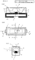
- Fig. 1 shows a known light-emitting apparatus that uses a wavelength conversion material.
- This light-emitting apparatus can include an insulating base 10, a semiconductor light-emitting device 12, and a light transmitting substrate 16 which is arranged on the insulating base 10.
- a pair of lead electrodes 11 can be formed on the surface of a substrate under the insulating base 10.
- the insulating base 10 can also have a concave portion 13 and a curved portion 14.
- the semiconductor light-emitting device 12 can be placed at the center of the bottom of the concave portion 13.
- the curved portion 14 can be continuous to the periphery of the concave portion 13.
- the semiconductor light-emitting device 12 placed at the center of the bottom of the concave portion 13 can be electrically connected with the pair of lead electrodes 11.
- a wavelength conversion layer 15 can be formed on a surface of the light transmitting substrate 16 where it faces the base 10.
- a reflecting film 17 made of Ag or the like can be formed on the inside of the concave portion 13 and the surface of the curved portion 14.
- the wavelength conversion layer 15 can be made of a resin in which phosphor materials are dispersed. The phosphor materials can be configured/selected for emitting light when excited by excitation light emitted from the semiconductor light-emitting device 12.
- the wavelength conversion layer 15 can be formed on the light transmitting substrate 16 by such means as screen printing.
- the light transmitting substrate 16 can be placed so that the wavelength conversion layer 15 is opposed to the semiconductor light-emitting device 12 and can be situated substantially directly above the concave portion 13 accommodating the device 12.
- the base 10 having the concave portion 13 and the curved portion 14 can, in conjunction with the light transmitting substrate 16 provided with the wavelength conversion layer 15, define a space which is filled with a translucent sealing material 18 to seal the semiconductor light-emitting device 12 and the wavelength conversion layer 15.
- the reflecting film 17 on the curved portion 14 may be coated with a second wavelength conversion layer 19 (for example, see Japanese Unexamined Patent Application Publication No. 2004-56075 A or its corresponding U.S. Patent No. 6,809,342 ).
- the concave portion 13 for accommodating the semiconductor light-emitting device and the curved portion 14 can and often should be formed for the sake of improved light emission efficiency.
- the light-emitting apparatus of this configuration is applied in a white chip LED (a surface mountable LED device emitting light in the white wavelength range) or the like for use in a liquid crystal display backlight of a cellular phone or mobile information terminal.
- the mold for forming the base 10 having the concave portion 13 and the curved portion 14 can and often should have a high degree of precision, and thus may require extremely high skill for fabrication. As a result, there have been problems relating to increased costs for the white chip LED, difficulty in manufacturing, etc.
- the light-emitting apparatus can develop unevenness in color inside.
- a reason for this is as follows: When the light-emitting apparatus is viewed from its optical axis, the color of the excitation light is dominant in an area immediately near the semiconductor light-emitting device 12. Meanwhile, the color complementary to that of the excitation light, occurring from the wavelength conversion layer, is dominant in surrounding areas somewhat away from the area immediately near the semiconductor light-emitting device 12. In terms of intensity (intensity distribution), there have been problems in that the intensity peaks at the area immediately near the semiconductor light-emitting device 12 and it decreases toward the periphery.
- the base 10 is provided with the concave portion 13 alone without the curved portion 14, and only the second wavelength conversion layer 19 is formed on the inside of the concave portion 13 without the first wavelength conversion layer 15.
- the light of the semiconductor light-emitting device 12 has difficulty in reaching the second wavelength conversion layer 19. Consequently, the complementary color of the excitation light, i.e., the light from the wavelength conversion layer 19 is dominant in the area immediately near the wavelength conversion layer 19 while the color of the light emitted from the semiconductor light-emitting device 12 is dominant in the other areas. That is, unevenness in color has also occurred in this case.
- intensity distribution there have also been problems similar to the intensity problems described above.
- WO 03/107441 A discloses an emitter package exhibiting limited wavelength variations between batches and consistent wavelength and emission characteristics with operation.
- the emitter package comprises a semiconductor emitter and a conversion material.
- the conversion material is arranged to absorb substantially all of the light emitting from the semiconductor emitter and re-emit light at one or more different wavelength spectrums of light.
- the conversion material is also arranged so that there is not an excess of conversion material to block said re-emitted light as it emits from said emitter package, said emitter package emitting light at said one or more wavelength spectrums from said conversion material.
- the semiconductor emitter is preferably a light emitting diode (LED) or laser diode.
- US 2003/0132701 A1 discloses a light emitting apparatus provided with a fluorescent substance sealed within a cured epoxy resin. More particularly, in a light emitting apparatus comprising a light emitting device, a fluorescent substance is provided which is capable of absorbing at least a portion of light emitted by the light emitting device and emitting light having a different wavelength, and a color converting member which contains the fluorescent substance and directly coat the light emitting device, the color converting member contains at least an epoxy resin derived from triazine and a mixing ratio of the epoxy resin derived from triazine to the acid anhydride curing agent in the color converting member is from 100:80 to 100:240.
- a mixing ratio of the epoxy resin derived from triazine to the acid anhydride curing agent in the color converting member is from 100:80 to 100:240.
- EP-A-1 107 321 discloses a light emitting diode comprising a light emitting diode element mounted on a glass epoxy substrate. The light emitting diode element is protected at its surface side by a resin seal member.
- a light emitting diode element for blue luminescence, formed of gallium nitride type compound semiconductor is used as the above-mentioned light emitting diode element; and a fluorescent material containing layer composed of a fluorescent material dispersed into an adhesive is arranged on the back side of this light emitting diode element. On the back side of the light emitting diode element, blue luminescence is converted in wavelength to produce white luminescence of high intensity.
- WO 03/034508 A discloses a light emitting device comprising a luminescent element and coating layers including a phosphor and provided in contact with each other. More particularly, a light emitting device comprises a luminescent element placed on a support and coating layers which bind a phosphor for absorbing a light from the luminescent element and converting the wave length thereof to the surface of the luminescent element, wherein the coating layers comprise an inorganic material comprising an oxide and a hydroxide of at least one element selected from the group consisting of Si, Al, Ga, Ti, Ge, P, B, Zr, Y, Sn, Pb and alkaline earth metals the light emitting device wherein the adhesive comprises the same inorganic material as that for the coating layers. Accordingly, there are no wavelength conversion layers separately formed on a bottom of a concave and in an opening thereof with a distance there between like the present invention.
- a semiconductor light-emitting apparatus is provided as forth in claim 1.
- the excitation light that is emitted in every direction from the semiconductor light-emitting device can generally undergo sufficient wavelength conversion before being emitted out of the light-emitting apparatus. This means a significant improvement to reducing color unevenness and intensity unevenness.
- the configuration capable of reducing intensity unevenness and suppressing the transmission of the near-ultraviolet light can prevent a light guide plate and the like from ultraviolet degradation.
- constituent light sources of white light such as blue light, are used as the excitation light source, it is possible to fabricate a white LED of reduced color unevenness and intensity unevenness.
- Fig. 1 is a schematic diagram showing a semiconductor light-emitting apparatus according to a known packaging technique
- Figs. 2A-2C are schematic diagrams showing an embodiment of a semiconductor light-emitting apparatus made in accordance with the principles of the present invention, where Fig. 2A is a sectional view taken along the line IIA-IIA of Fig. 2B, Fig. 2B is a schematic plan view, and Fig. 2C is a sectional view taken along the line IIC-IIC of Fig. 2B ;
- Fig. 3 is a diagram showing the intensity distribution of a comparative example of the semiconductor light-emitting apparatus of Figs. 2A-2C ;
- Fig. 4 is a diagram showing the intensity distribution of a particular fabrication of the semiconductor light-emitting apparatus of Figs. 2A-2C ;
- FIGs. 5A and 5B are schematic diagrams showing another embodiment of a semiconductor light-emitting apparatus made in accordance with the principles of the invention, where Fig. 5A is a sectional view of the same, and Fig. 5B is a plan view of the same;
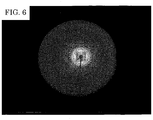
- Fig. 6 is a diagram showing the intensity distribution of a comparative example of the semiconductor light-emitting apparatus of Figs. 5A-B ;
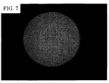
- Fig. 7 is a diagram showing the intensity distribution of a particular fabrication of the semiconductor light-emitting apparatus of Figs. 5A-B ;
- Fig. 8 is a chart showing the emission spectra of the light emitted from a particular fabrication of a semiconductor light-emitting apparatus of Figs. 5A-B as compared to a comparative semiconductor light-emitting apparatus.
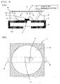
- Figs. 2A-2C are explanatory diagrams showing an embodiment of the semiconductor light-emitting apparatus made in accordance with the principles of the invention.
- Fig. 2A is a sectional view taken along the line IIA-IIA of Fig. 2B.
- Fig. 2B is a schematic plan view.
- Fig. 2C is a sectional view taken along the line IIC-IIC of Fig. 2B .
- the semiconductor light-emitting apparatus of Fig. 2A can include an insulating base 7, a semiconductor light-emitting device 1, and a wavelength conversion portion.
- the insulating base 7 can also include a concave portion 6.
- the semiconductor light-emitting device 1 can be arranged at the bottom of the concave portion 6.
- the wavelength conversion portion can be composed of a first wavelength conversion layer 3 formed on the bottom of the concave portion 6, and a second wavelength conversion layer 5 formed in the opening of the concave portion 6 at a distance above the semiconductor light-emitting device 1.
- the space defined by the concave portion 6 of the base 7 and the second wavelength conversion layer 5 can be filled with a sealing material 4 for transmitting light emitted from the semiconductor light-emitting device 1.
- the base 7 can include and/or consist of a substrate part 7a and a reflecting frame part 7b.
- the substrate part 7a can be provided with at least a pair of lead electrodes 8, or an anode electrode and a cathode electrode.
- the lead electrodes 8 can project out of the base 7.
- the reflecting frame part 7b can be arranged on the substrate part 7a and can have the concave portion 6 in its center.
- the pair of lead electrodes 8 can be formed so that the electrodes 8 are exposed in the bottom area of the concave portion 6.
- the semiconductor light-emitting device is surrounded by the reflecting frame part 7b, and the concave portion 6 is formed in the center of the same.
- the reflecting frame part 7b may be formed in other manners, including on either one of the pairs of opposed sides and not on the other.
- the reflecting frame part 7b can be formed on the right and left alone, and not on the top and bottom.
- the concave portion 6 can be formed in the middle.
- Examples of the methods for forming the concave portion 6 into which the semiconductor light-emitting device 1 can be arranged and fixed are, though not restrictive, described as follows.
- Integral molding methods can be used such that the electrodes 8 are loaded as insert members into a mold, and the material is injected into the mold so that the base 7 (the substrate part 7a and the reflecting frame part 7b) is insert-molded.
- Bonding-after methods can be used such that the electrodes 8 are fixed to the surface of the substrate part 7a before the reflecting frame part 7b is attached to form the base 7.
- the material(s) for making the base 7 can be selected from among ones that develop no electric short circuit between the anode and cathode electrodes, or the lead electrodes 8.
- the substrate part 7a can be made of an insulating material such as insulating resins including a glass fiber containing epoxy resin, and ceramics. In a practical viewpoint, it is sometimes preferable to use materials having relatively high melting points so that no deformation occurs at temperatures expected at the time of packaging with solder materials.
- the reflecting frame part 7b can be made of an insulating material having heat resistance to soldering temperatures (around 200°C or below), such as high melting point insulating resins made of liquid polymers including liquid crystal polyester, and ceramics.
- the concave portion 6 may also be preferable for the concave portion 6 to be formed in the center, and that the material be white or the like in color, having a certain degree of high reflectivity.
- the substrate part 7a and the reflecting frame part 7b can be made of liquid crystal polymers. White liquid crystal polymer materials are sometimes superior in many respects, including insulation performance, heat resistance, high reflectivity, and formability.
- a layer of high reflectivity material may be formed on the inside 71 of the concave portion 6 of the base 7 by such means as coating, plating, vapor deposition, and the like.
- the concave portion 6 may be shaped generally like a truncated cone, a truncated pyramid, partially hemispherical surface, etc.
- the concave portion 6 can also have an inclined inner periphery.
- the inner periphery may be shaped generally perpendicular for the sake of a desired reduction in device profile.
- the reflecting frame part 7b can be generally rectangular in the angle of the inner periphery without departing from the spirit and scope of the invention.
- the semiconductor light-emitting device 1 can be attached to the bottom of the concave portion 6.
- the semiconductor light-emitting device 1 is electrically and mechanically fixed onto one of the electrodes 8 by die bonding using an Ag paste.
- a conductive wire 2 that extends from the top of the semiconductor light-emitting device and the other electrode 8 can be connected by wire bonding.
- the semiconductor light-emitting device 1 may be made of any semiconductor material, and preferably of a material that emits light having energy capable of exciting the wavelength conversion material. Semiconductor materials for emitting light in the range of ultraviolet light and blue light are preferable in particular instances. It is also sometimes preferable that the semiconductor light-emitting device 1 fall within the range of 300 and 490 nm in the light emission peak wavelength.
- Examples of the semiconductor materials for making the semiconductor light-emitting device 1 include light-emitting diodes (LEDs) such as group-III nitride compound (for example, In-Ga-Al-N compound) semiconductors, zinc oxide compound (for example, Zn-Mg-O compound) semiconductors, zinc selenide compound (for example, Zn-Mg-Se-S-Te compound) semiconductors, and silicon carbide compound (for example, Si-Ge-C) semiconductors.
- LEDs light-emitting diodes
- group-III nitride compound for example, In-Ga-Al-N compound
- zinc oxide compound for example, Zn-Mg-O compound
- zinc selenide compound for example, Zn-Mg-Se-S-Te compound
- silicon carbide compound for example, Si-Ge-C semiconductors.
- the semiconductor materials are not limited thereto. It is only preferable in certain circumstances that they emit light within the foregoing range of light emission peak wavelengths.
- Figs. 2A-2C deals with the case where the bottom side of the semiconductor light-emitting device 1 establishes electric connection with one of the electrodes 8, and the top side establishes electric connection with the other electrode 8. It is also possible, however, to use a semiconductor device that can establish electric connection with both the electrodes 8 at an identical side, or to different combinations of side, bottom or top mount electrodes.
- the semiconductor light-emitting device can be mechanically bonded onto the substrate part 7a with an adhesive such as an epoxy resin.
- the anode and cathode electrodes formed on the top side of the semiconductor light-emitting device can be electrically bonded to the respective corresponding lead electrodes 8 in pair by conductive wires 2.
- the anode and cathode electrodes of the semiconductor light-emitting device 1 are electrically connected to the corresponding lead electrodes 8 and the device is fixed to the base 7 at the same time by such means as Au-Sn or other eutectic materials, Au bumps, anisotropic conductive sheets, and conductive resins typified by an Ag paste; and those in which either one of the electrodes of the device is electrically connected to the corresponding lead electrode 8 and fixed to the base 7 by using the foregoing materials while the other electrode and the corresponding lead electrode 8 are electrically bonded by a conductive wire.
- the base 7 may be made of metal or other conductive materials.
- the base 7 may also function as one of the lead electrodes 8.
- the base 7, the semiconductor light-emitting device 1, and the lead electrodes 8 There are various forms available for the base 7, the semiconductor light-emitting device 1, and the lead electrodes 8. Regardless of the form that is used, the semiconductor light-emitting device 1 can be fixed onto the base 7, and the anode and cathode lead electrodes 8 can be electrically connected to the corresponding anode and cathode electrodes of the semiconductor light-emitting device 1.
- the first wavelength conversion layer 3 can be formed in the bottom area of the concave portion 6. In the example shown in Figs. 2A-2C , the first wavelength conversion layer 3 is formed on the top area of the substrate part 7a and on the semiconductor light-emitting device 1 at the bottom of the concave portion 6.
- the first wavelength conversion layer 3 can have one or more layers of wavelength conversion materials within a thickness smaller than the height of the semiconductor light-emitting device 1. The ideal thickness depends on various properties, including the wavelength conversion efficiencies of various wavelength conversion materials. In a practical viewpoint, the wavelength conversion layer can have a thickness around 20 to 200 ⁇ m since the semiconductor light-emitting device generally has a thickness of 300 ⁇ m or so.
- the "wavelength conversion portion (or layer)" will refer not only to the layer made of wavelength conversion material alone, but also to the entire area where wavelength conversion material concentrates densely.
- the wavelength conversion layer can refer to an entire area of the sealing portion 4 to be described later where the phosphor particles are distributed densely.
- the first wavelength conversion layer 3 may be formed by any of the following methods: (1) placing the semiconductor light-emitting device 1 on the bottom of the concave portion 6, and then applying a wavelength conversion material such as an inorganic phosphor directly to the bottom of the concave portion 6 to form the first wavelength conversion layer 3; (2) mixing the wavelength conversion material for forming the first wavelength conversion layer 3 into the material for forming the sealing portion 4, injecting the mixed material into the concave portion 6, and hardening the sealing portion 4 when the wavelength conversion material in the mixed material settles out to the bottom area of the concave portion 6 by its own weight and lies densely in this area, so that this area creates the first wavelength conversion layer 3; and (3) attaching, onto the bottom of the concave portion 6a, a wavelength-conversion-material-containing sheet that has a predetermined thickness and a wavelength conversion material at a predetermined density.
- a wavelength conversion material such as an inorganic phosphor
- the first wavelength conversion layer 3 can also be formed on the top of the semiconductor light-emitting device 1.
- the semiconductor light-emitting apparatus can be improved by providing a more even intensity distribution due to the excitation light being emitted directly upward from the semiconductor light-emitting device 1. This configuration allows light to be wavelength converted and scattered as well.
- the first wavelength conversion layer 3 has approximately the same thickness throughout the layer.
- distribution of phosphors that form the first wavelength conversion layer 3 is not limited thereto, and can include various thickness layers and layers that have changing thicknesses.
- the sealing portion 4 can be made of a light transmitting material which maintains the distance from the semiconductor light-emitting device 1 and the first wavelength conversion layer 3 to the second wavelength conversion layer 5.
- the material may also be capable of transmitting both the excitation light from the semiconductor light-emitting device 1 and the wavelength conversion light converted by the wavelength conversion material.
- Some examples include thermosetting resins and low melting point glass.
- the sealing portion 4 may be formed to be hollow (or sealed with a gaseous material) when accompanied with a configuration that fixes the sheet to the reflecting frame part 7b.
- Examples of materials that can be used for making the sealing portion 4 are the following: materials that have a high transmittance up to shortwave regions covering the peak wavelength of light emission from the semiconductor light-emitting device 1; materials that have a constituent material of the first wavelength conversion layer 3 that can be mixed and dispersed therein; and materials in which the constituent material of the first wavelength conversion layer 3 can settle out (be distributed) densely at the bottom of the concave portion 6 when heated and left standing, etc.
- Specific examples include thermosetting resins containing at least one resin selected from the group consisting of epoxy resins, silicone resins, polydimethylsiloxane derivatives having epoxy groups, oxetane resins, acryl resins, and cycloolefin resins.
- epoxy resins made of epoxy resin materials containing hydrogenated bisphenol A diglycidyl ether, alycyclic epoxy carboxylate, and organic sulfonium-hexafluoroantimonate can be used.
- the sealing portion 4 can be shaped so that its top surface that corresponds to a position substantially directly above the semiconductor light-emitting device 1 sinks into a generally recessed surface. This can facilitate the formation of the second wavelength conversion layer 5.
- the second wavelength conversion layer 5 can efficiently scatter the excitation light and the once-wavelength-converted light which is wavelength-converted by the first wavelength conversion layer 3.
- Examples of methods that can be used to form a generally recessed surface on the sealing portion 4 are as follows: heating the material of the sealing portion 4 for hardening, at which time the surface is formed naturally through solvent evaporation; controlling the composition of the material of the sealing portion 4 and the amount of injection of the same to cause a meniscus phenomenon, and harden it in that state to form the recessed surface; and forming the recessed surface by compression molding or the like.
- the second wavelength conversion layer 5 can be arranged at an appropriate distance from the semiconductor light-emitting device 1 and the first wavelength conversion layer 3 so that it covers the vicinity of the opening end of the concave portion 6 (see Fig. 2A ), at least over the semiconductor light-emitting device 1 in plan view.
- the second wavelength conversion layer 5 is arranged at the center of the opening of the concave portion 6 and has an area narrower than the opening.
- the second wavelength conversion layer 5 is formed to cover the entire opening of the concave portion 6.
- the second wavelength conversion layer 5 can be formed by mixing an appropriate binder resin and a wavelength conversion material, and arranging this mixed material onto the sealing portion 4 directly above the semiconductor light-emitting device 1 by such means as potting using a dispenser.
- the sealing portion 4 can be shaped so that its top sinks into a generally curved surface.
- the recess formed in the top of the sealing portion 4 can be filled with the constituent material of the second wavelength conversion layer 5 to form the second wavelength conversion layer 5.
- the binder resin of the second wavelength conversion layer 5 may be the same material as the constituent material of the sealing portion 4. Any material may be used and preferably has excellent adhesiveness with the sealing portion 4 and causes little or no degradation due to the excitation light.
- the thickness of the second wavelength conversion layer 5 even a single layer of particles of the wavelength conversion material is effective. Since excessive thicknesses can lower the output efficiency, a thickness in the range of 20 ⁇ m to 150 ⁇ m may be desirable in some circumstances. A thickness that is smaller than that of the first wavelength conversion layer 3 is also often preferable.
- the wavelength conversion materials for forming the first wavelength conversion layer 3 and the second wavelength conversion layer 5 convert the peak wavelength of light emission from the semiconductor light-emitting device 1 into longer peak wavelengths of light emission.
- the wavelength conversion materials may contain one or more types of materials. In consideration of color unevenness, the first wavelength conversion layer 3 and the second wavelength conversion layer 5 can be made of the same wavelength conversion material. Nevertheless, the first wavelength conversion layer 3 and the second wavelength conversion layer 5 may be made of respective different wavelength conversion materials, depending on the physical properties of the constituent materials, such as reflectance. Examples of wavelength conversion materials include the following.
- a 3 B 5 O 12 :M phosphors (A: at least one element selected from among Y, Gd, Lu, and Tb; B: at least one element selected from A1 and Ga; and M: at least one ion selected from among Ce 3+ , Tb 3+ , Eu 3+ , Cr 3+ , Nd 3+ , and Er 3+ ); rare-earth doped barium-aluminum-magnesium compound phosphors (BAM phosphors); sulfide compound phosphors typified by Y 2 O 2 S:Eu 3+ and ZnS:Cu,Al; rare-earth doped thiogallate phosphors such as (Sr,Ca)S:Eu 2+ , CaGa 2 S 4 :Eu 2+ , and SrGa 2 S 4 :Eu 2+ ; and phosphors containing at least one of aluminate compositions such as TbAlO 3 :Ce 3+ .
- the wavelength conversion layers may include scattering agents such as barium sulfate, magnesium oxide, and/or silicon oxide for the sake of assisting the reflection of the excitation light and the wavelength conversion light.
- the excitation light can undergo the same wavelength conversion, reflection, etc. as in the foregoing case where the excitation light constitutes a light source of white light.
- the light can be emitted from the opening of the concave portion 6.
- the excitation light is in the ultraviolet or near-ultraviolet region, however, the external emission of the excitation light can cause the ultraviolet degradation of electronic parts such as a light guide plate. It may therefore be preferable to prevent the excitation light from being emitted outside of the light-emitting apparatus as much as possible.
- the thicknesses and constituent materials of the first wavelength conversion layer 3 and the second wavelength conversion layer 5 be adjusted to reduce ultraviolet rays to be emitted outside.
- the external emission of the ultraviolet rays can also be reduced by configuring the semiconductor light-emitting apparatus so that the light emitted from the semiconductor light-emitting device always takes the path through the first wavelength conversion layer 3 and/or the second wavelength conversion layer 5.
- the second wavelength conversion layer 5 is arranged to cover the entire opening of the concave portion 6 so that all the emitted light can be turned into wavelength conversion light.
- a semiconductor light-emitting apparatus having an oblong rectangular shape in plan view as shown in Figs. 2A and 2B was fabricated.
- a description of this specific fabrication is now provided as an example of an apparatus and method that corresponds to the embodiment shown in Figs. 2A-C .
- a white thermosetting resin having a high melting point was insert molded with Ag-plated lead electrodes 8 as the insert members.
- a base 7 having a concave portion 6 and integrated electrodes 8 was fabricated.
- IIC-IIC shown in Fig.
- the concave portion 6 was formed so that the top surfaces of the lead electrodes 8 and the inside of the concave portion 6 of the reflecting frame part 7b formed an angle of approximately 90°. Furthermore, in the section taken along the line IIA-IIA of Fig. 2A , the concave portion 6 was formed so that the top surfaces of the lead electrodes 8 and the inside of the concave portion 6 of the reflecting frame part 7b formed an obtuse angle.
- a semiconductor device for emitting blue light made of an InGaN compound semiconductor (having a light emission peak wavelength of 470 nm) formed on an n-type SiC substrate, was used.
- a cathode electrode formed on this n-type substrate and its corresponding lead electrode 8 were electrically bonded to each other and mechanically fixed to the base 7 with an Ag paste.
- an epoxy resin was mixed with an appropriate amount of YAG phosphor to form the constituent material.
- YAG phosphors generate wavelength conversion light of yellow when excited by blue light of near 470 nm.
- This constituent material was filled into the concave portion 6, and left standing so that the phosphor naturally settled out to the bottom area of the concave portion 6. Then, under the condition of 150°C and after hour, the material was hardened to simultaneously form the first wavelength conversion layer 3 and the sealing portion 4.
- the constituent material of the second wavelength conversion layer 5 i.e., a mixed material of epoxy resin and the previously described phosphor, was applied to a recess in the top of the sealing portion 4 which had been generated by itself during the hardening of the epoxy resin.
- the resultant mixture was hardened at 150°C for one hour, to form the second wavelength conversion layer 5.
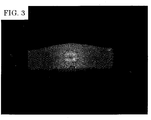
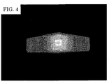
- Fig. 4 shows the intensity distribution of the semiconductor light-emitting apparatus, as viewed from its optical axis, when the semiconductor light-emitting device as described in the above fabrication description was energized and lit by a current of 1 mA.
- white areas have higher intensities, and black areas lower intensities.
- a semiconductor light-emitting apparatus having the same oblong rectangular shape was fabricated under the same condition as in the above described configuration/fabrication of the embodiment of Figs. 2A-C .
- the first wavelength conversion layer 3 and the sealing portion 4 were formed under the same conditions, whereas the second wavelength conversion layer 5 was not formed.
- Fig. 3 shows the intensity distribution of the semiconductor light-emitting apparatus, as viewed from its optical axis, when the semiconductor light-emitting device of the comparative example (without the second wavelength conversion layer 5) was energized and lit by the same current of 1 mA. Again, in Fig. 3 , white areas have higher intensities, and black areas lower intensities.
- the semiconductor light-emitting apparatus used to create the light intensity distribution of Fig. 4 showed more uniform white light emission over almost all areas, with no noticeable unevenness in intensity distribution as compared to that of Fig. 3 .
- FIG. 5A and 5B A description of this specific fabrication (fabrication II) is now provided as an example of an apparatus and method that corresponds to the embodiment shown in Figs. 5A-B .
- a white thermosetting resin having a high melting point was insert molded with Ag-plated lead electrodes 8 as the insert members.
- a base 7 having a concave portion 6 and integrated electrodes 8 was fabricated.
- the concave portion 6 was shaped like a bowl so that the top surfaces of the lead electrodes 8 and the inside of the concave portion 6 of the reflecting frame part 7b formed an angle of approximately 50°.
- a semiconductor device for emitting ultraviolet rays made of an InGaN compound semiconductor (having a light emission peak wavelength of 395 nm) formed on an n-type SiC substrate, was used.
- a cathode electrode formed on this n-type substrate and its corresponding lead electrode 8 were electrically bonded to each other and mechanically fixed to the base 7 with an Ag paste.
- predetermined proportions of blue, red, and green light emission phosphors, or a barium-aluminum-magnesium compound phosphor (BAM phosphor), Y 2 O 2 S:Eu 3+ , and ZnS:Cu,Al, respectively, were mixed to form a wavelength conversion material.
- the thus obtained mixed phosphors were mixed and dispersed into an epoxy resin at a rate of 20% by weight.
- the employed epoxy resin contained a certain amount of UV absorbents. Alternatively, it can be noted that resin having high UV resistance by itself may have been used.
- the resulting constituent material was filled into the concave portion 6, and left standing so that the phosphors naturally settled out to the bottom area of the concave portion 6. Then, under the condition of 150°C and after 1 hour, the material was hardened to simultaneously form the first wavelength conversion layer 3 and the sealing portion 4.
- the constituent material of the second wavelength conversion layer 5 i.e., the mixed material that included epoxy resin and 20% by weight of the foregoing described mixed phosphors, was applied to a recess in the top of the sealing portion 4 which had been generated by itself during the hardening of the epoxy resin.
- the resultant material was hardened at 150°C for one hour to form the second wavelength conversion layer 5.
- the second wavelength conversion layer 5 was formed only in the center area of the opening of the concave portion 6, not in the surrounding areas.
- the second wavelength conversion layer 5 was formed over the entire opening of the concave portion 6 as shown in Figs. 5A and 5B .
- the first wavelength conversion layer 3 and the second wavelength conversion layer 5 both had a thickness of approximately 130 ⁇ m.
- Fig. 7 shows the intensity distribution of the semiconductor light-emitting apparatus, as viewed from its optical axis, when the above-described fabrication II of the semiconductor light-emitting device was energized and lit by a current of 1 mA.
- white areas have higher intensities, and black areas lower intensities.
- a semiconductor light-emitting apparatus having the same square shape was fabricated under the same conditions as in fabrication II.
- the first wavelength conversion layer 3 and the sealing portion 4 were formed under the same conditions, whereas the second wavelength conversion layer 5 was not formed.
- Fig. 6 shows the intensity distribution of the semiconductor light-emitting apparatus, as viewed from its optical axis, when the semiconductor light-emitting device of the comparative example to fabrication II was energized and lit by the same current of 1 mA as was used with fabrication II. Again, in Fig. 6 , white areas have higher intensities, and black areas lower intensities.
- a spectral analysis was conducted on the light emitted from the semiconductor light-emitting apparatuses of the fabrication II device and the comparative example to fabrication II device.
- Fig. 8 shows the results.
- the semiconductor light-emitting apparatuses were installed in the integrating sphere of a spectroscopic analyzer, energized by a current of 20 mA, and measured for the light emitted at that time.
- the light emitted from the semiconductor light-emitting apparatus according to fabrication II contains 50% or less excitation light, i.e., light having a peak wavelength of 395 nm, as compared to the comparative example to fabrication II described above where the second wavelength conversion layer is not formed.
Description
- The present invention relates to a light-emitting apparatus having a semiconductor light-emitting device. In particular, the invention relates to a semiconductor light-emitting apparatus in which a semiconductor light-emitting device, or excitation light source, and a wavelength conversion portion are combined to chiefly emit white light.
-
Fig. 1 shows a known light-emitting apparatus that uses a wavelength conversion material. This light-emitting apparatus can include aninsulating base 10, a semiconductor light-emitting device 12, and a light transmittingsubstrate 16 which is arranged on theinsulating base 10. A pair oflead electrodes 11 can be formed on the surface of a substrate under theinsulating base 10. Theinsulating base 10 can also have aconcave portion 13 and acurved portion 14. The semiconductor light-emitting device 12 can be placed at the center of the bottom of theconcave portion 13. Thecurved portion 14 can be continuous to the periphery of theconcave portion 13. The semiconductor light-emitting device 12 placed at the center of the bottom of theconcave portion 13 can be electrically connected with the pair oflead electrodes 11. Awavelength conversion layer 15 can be formed on a surface of thelight transmitting substrate 16 where it faces thebase 10. - For the sake of efficient light reflection, a reflecting
film 17 made of Ag or the like can be formed on the inside of theconcave portion 13 and the surface of thecurved portion 14. Thewavelength conversion layer 15 can be made of a resin in which phosphor materials are dispersed. The phosphor materials can be configured/selected for emitting light when excited by excitation light emitted from the semiconductor light-emitting device 12. Thewavelength conversion layer 15 can be formed on thelight transmitting substrate 16 by such means as screen printing. Thelight transmitting substrate 16 can be placed so that thewavelength conversion layer 15 is opposed to the semiconductor light-emitting device 12 and can be situated substantially directly above theconcave portion 13 accommodating thedevice 12. Thebase 10 having theconcave portion 13 and thecurved portion 14 can, in conjunction with thelight transmitting substrate 16 provided with thewavelength conversion layer 15, define a space which is filled with atranslucent sealing material 18 to seal the semiconductor light-emitting device 12 and thewavelength conversion layer 15. Incidentally, the reflectingfilm 17 on thecurved portion 14 may be coated with a second wavelength conversion layer 19 (for example, seeJapanese Unexamined Patent Application Publication No. 2004-56075 A U.S. Patent No. 6,809,342 ). - In the light-emitting apparatus described above, the
concave portion 13 for accommodating the semiconductor light-emitting device and thecurved portion 14 can and often should be formed for the sake of improved light emission efficiency. Suppose, for example, the light-emitting apparatus of this configuration is applied in a white chip LED (a surface mountable LED device emitting light in the white wavelength range) or the like for use in a liquid crystal display backlight of a cellular phone or mobile information terminal. The mold for forming thebase 10 having theconcave portion 13 and thecurved portion 14 can and often should have a high degree of precision, and thus may require extremely high skill for fabrication. As a result, there have been problems relating to increased costs for the white chip LED, difficulty in manufacturing, etc. - With an extremely simple configuration in which the first
wavelength conversion layer 15 is formed alone without thecurved portion 14 or the secondwavelength conversion layer 19, the light-emitting apparatus can develop unevenness in color inside. A reason for this is as follows: When the light-emitting apparatus is viewed from its optical axis, the color of the excitation light is dominant in an area immediately near the semiconductor light-emitting device 12. Meanwhile, the color complementary to that of the excitation light, occurring from the wavelength conversion layer, is dominant in surrounding areas somewhat away from the area immediately near the semiconductor light-emitting device 12. In terms of intensity (intensity distribution), there have been problems in that the intensity peaks at the area immediately near the semiconductor light-emitting device 12 and it decreases toward the periphery. - Next, we will analyze the case where the
base 10 is provided with theconcave portion 13 alone without thecurved portion 14, and only the secondwavelength conversion layer 19 is formed on the inside of theconcave portion 13 without the firstwavelength conversion layer 15. Here, when the light-emitting apparatus is viewed from its optical axis, the light of the semiconductor light-emitting device 12 has difficulty in reaching the secondwavelength conversion layer 19. Consequently, the complementary color of the excitation light, i.e., the light from thewavelength conversion layer 19 is dominant in the area immediately near thewavelength conversion layer 19 while the color of the light emitted from the semiconductor light-emitting device 12 is dominant in the other areas. That is, unevenness in color has also occurred in this case. As for intensity distribution, there have also been problems similar to the intensity problems described above. -
WO 03/107441 A -
US 2003/0132701 A1 discloses a light emitting apparatus provided with a fluorescent substance sealed within a cured epoxy resin. More particularly, in a light emitting apparatus comprising a light emitting device, a fluorescent substance is provided which is capable of absorbing at least a portion of light emitted by the light emitting device and emitting light having a different wavelength, and a color converting member which contains the fluorescent substance and directly coat the light emitting device, the color converting member contains at least an epoxy resin derived from triazine and a mixing ratio of the epoxy resin derived from triazine to the acid anhydride curing agent in the color converting member is from 100:80 to 100:240. However, there are no separate wavelength conversion layers like the present invention. -
EP-A-1 107 321 discloses a light emitting diode comprising a light emitting diode element mounted on a glass epoxy substrate. The light emitting diode element is protected at its surface side by a resin seal member. A light emitting diode element for blue luminescence, formed of gallium nitride type compound semiconductor is used as the above-mentioned light emitting diode element; and a fluorescent material containing layer composed of a fluorescent material dispersed into an adhesive is arranged on the back side of this light emitting diode element. On the back side of the light emitting diode element, blue luminescence is converted in wavelength to produce white luminescence of high intensity. -
WO 03/034508 A - To solve the foregoing and other related problems, intensive studies have been made to obtain equivalent or better properties from light emitting devices. As a result, the above and/or other problems can be solved or mediated by the provision of different embodiments of the invention.
- According to an aspect of the invention, a semiconductor light-emitting apparatus is provided as forth in
claim 1. - According to another aspect of the invention, there can be provided a method of fabricating a semiconductor light-emitting apparatus as set forth in claim 9.
- Preferred embodiments of the present invention may be gathered from the dependent claims.
- In accordance with the present invention, it is possible to fabricate a semiconductor light-emitting apparatus of low profile with great ease and/or at low cost.
- Moreover, it is possible to obtain light emission with significantly high efficiency as compared to apparatuses that utilize only the light transmitted through a wavelength conversion layer or only the light reflected from a wavelength conversion layer. Moreover, since the process of forming a curved area in the concave portion may not be required, a low-profile apparatus can be fabricated at low cost. In addition, light-emitting apparatuses of this type can be manufactured by using conventional LED lead frames as is, which can eliminate the need for special molds.
- The excitation light that is emitted in every direction from the semiconductor light-emitting device can generally undergo sufficient wavelength conversion before being emitted out of the light-emitting apparatus. This means a significant improvement to reducing color unevenness and intensity unevenness. In particular, when near-ultraviolet light is used as the excitation light source, the configuration capable of reducing intensity unevenness and suppressing the transmission of the near-ultraviolet light can prevent a light guide plate and the like from ultraviolet degradation. Moreover, when constituent light sources of white light, such as blue light, are used as the excitation light source, it is possible to fabricate a white LED of reduced color unevenness and intensity unevenness.
- These and other objects, features, and advantages of the present invention will become clear from the following description of exemplary embodiments and with reference to the accompanying drawings, wherein:
-
Fig. 1 is a schematic diagram showing a semiconductor light-emitting apparatus according to a known packaging technique; -
Figs. 2A-2C are schematic diagrams showing an embodiment of a semiconductor light-emitting apparatus made in accordance with the principles of the present invention, whereFig. 2A is a sectional view taken along the line IIA-IIA ofFig. 2B, Fig. 2B is a schematic plan view, andFig. 2C is a sectional view taken along the line IIC-IIC ofFig. 2B ; -
Fig. 3 is a diagram showing the intensity distribution of a comparative example of the semiconductor light-emitting apparatus ofFigs. 2A-2C ; -
Fig. 4 is a diagram showing the intensity distribution of a particular fabrication of the semiconductor light-emitting apparatus ofFigs. 2A-2C ; -
Figs. 5A and 5B are schematic diagrams showing another embodiment of a semiconductor light-emitting apparatus made in accordance with the principles of the invention, whereFig. 5A is a sectional view of the same, andFig. 5B is a plan view of the same; -
Fig. 6 is a diagram showing the intensity distribution of a comparative example of the semiconductor light-emitting apparatus ofFigs. 5A-B ; -
Fig. 7 is a diagram showing the intensity distribution of a particular fabrication of the semiconductor light-emitting apparatus ofFigs. 5A-B ; and -
Fig. 8 is a chart showing the emission spectra of the light emitted from a particular fabrication of a semiconductor light-emitting apparatus ofFigs. 5A-B as compared to a comparative semiconductor light-emitting apparatus. - Hereinafter, description will be given of the present invention with reference to the drawing figures, wherein like reference numerals designate identical or corresponding elements throughout the several figures. Incidentally, various modifications can be made without departing from the gist of the invention. It is intended that various modifications of the exemplary embodiments described herein can be made and would fall within the scope of the present invention.
-
Figs. 2A-2C are explanatory diagrams showing an embodiment of the semiconductor light-emitting apparatus made in accordance with the principles of the invention.Fig. 2A is a sectional view taken along the line IIA-IIA ofFig. 2B. Fig. 2B is a schematic plan view.Fig. 2C is a sectional view taken along the line IIC-IIC ofFig. 2B . - The semiconductor light-emitting apparatus of
Fig. 2A can include an insulatingbase 7, a semiconductor light-emittingdevice 1, and a wavelength conversion portion. The insulatingbase 7 can also include aconcave portion 6. The semiconductor light-emittingdevice 1 can be arranged at the bottom of theconcave portion 6. Here, the wavelength conversion portion can be composed of a firstwavelength conversion layer 3 formed on the bottom of theconcave portion 6, and a secondwavelength conversion layer 5 formed in the opening of theconcave portion 6 at a distance above the semiconductor light-emittingdevice 1. The space defined by theconcave portion 6 of thebase 7 and the secondwavelength conversion layer 5 can be filled with a sealingmaterial 4 for transmitting light emitted from the semiconductor light-emittingdevice 1. - The
base 7 can include and/or consist of a substrate part 7a and a reflectingframe part 7b. The substrate part 7a can be provided with at least a pair oflead electrodes 8, or an anode electrode and a cathode electrode. Thelead electrodes 8 can project out of thebase 7. The reflectingframe part 7b can be arranged on the substrate part 7a and can have theconcave portion 6 in its center. The pair oflead electrodes 8 can be formed so that theelectrodes 8 are exposed in the bottom area of theconcave portion 6. In the shown example, the semiconductor light-emitting device is surrounded by the reflectingframe part 7b, and theconcave portion 6 is formed in the center of the same. Nevertheless, the reflectingframe part 7b may be formed in other manners, including on either one of the pairs of opposed sides and not on the other. For example, in the plan view ofFig. 2B , the reflectingframe part 7b can be formed on the right and left alone, and not on the top and bottom. Theconcave portion 6 can be formed in the middle. - Examples of the methods for forming the
concave portion 6 into which the semiconductor light-emittingdevice 1 can be arranged and fixed are, though not restrictive, described as follows. - Integral molding methods can be used such that the
electrodes 8 are loaded as insert members into a mold, and the material is injected into the mold so that the base 7 (the substrate part 7a and the reflectingframe part 7b) is insert-molded. - Bonding-after methods can be used such that the
electrodes 8 are fixed to the surface of the substrate part 7a before the reflectingframe part 7b is attached to form thebase 7. - The material(s) for making the
base 7 can be selected from among ones that develop no electric short circuit between the anode and cathode electrodes, or thelead electrodes 8. The substrate part 7a can be made of an insulating material such as insulating resins including a glass fiber containing epoxy resin, and ceramics. In a practical viewpoint, it is sometimes preferable to use materials having relatively high melting points so that no deformation occurs at temperatures expected at the time of packaging with solder materials. The reflectingframe part 7b can be made of an insulating material having heat resistance to soldering temperatures (around 200°C or below), such as high melting point insulating resins made of liquid polymers including liquid crystal polyester, and ceramics. It may also be preferable for theconcave portion 6 to be formed in the center, and that the material be white or the like in color, having a certain degree of high reflectivity. For integral molding, the substrate part 7a and the reflectingframe part 7b can be made of liquid crystal polymers. White liquid crystal polymer materials are sometimes superior in many respects, including insulation performance, heat resistance, high reflectivity, and formability. In addition, a layer of high reflectivity material may be formed on the inside 71 of theconcave portion 6 of thebase 7 by such means as coating, plating, vapor deposition, and the like. - The
concave portion 6 may be shaped generally like a truncated cone, a truncated pyramid, partially hemispherical surface, etc. Theconcave portion 6 can also have an inclined inner periphery. However, in the case of a white LED intended for use as a light source of a display backlight in a cellular phone, the inner periphery may be shaped generally perpendicular for the sake of a desired reduction in device profile. Thus, the reflectingframe part 7b can be generally rectangular in the angle of the inner periphery without departing from the spirit and scope of the invention. - The semiconductor light-emitting
device 1 can be attached to the bottom of theconcave portion 6. In the example shown inFigs. 2A-2C , the semiconductor light-emittingdevice 1 is electrically and mechanically fixed onto one of theelectrodes 8 by die bonding using an Ag paste. Aconductive wire 2 that extends from the top of the semiconductor light-emitting device and theother electrode 8 can be connected by wire bonding. - The semiconductor light-emitting
device 1 may be made of any semiconductor material, and preferably of a material that emits light having energy capable of exciting the wavelength conversion material. Semiconductor materials for emitting light in the range of ultraviolet light and blue light are preferable in particular instances. It is also sometimes preferable that the semiconductor light-emittingdevice 1 fall within the range of 300 and 490 nm in the light emission peak wavelength. Examples of the semiconductor materials for making the semiconductor light-emittingdevice 1 include light-emitting diodes (LEDs) such as group-III nitride compound (for example, In-Ga-Al-N compound) semiconductors, zinc oxide compound (for example, Zn-Mg-O compound) semiconductors, zinc selenide compound (for example, Zn-Mg-Se-S-Te compound) semiconductors, and silicon carbide compound (for example, Si-Ge-C) semiconductors. However, the semiconductor materials are not limited thereto. It is only preferable in certain circumstances that they emit light within the foregoing range of light emission peak wavelengths. Incidentally, semiconductor light-emitting devices fixed onto sub mounts shall also be referred to as "semiconductor light-emitting devices" and fall within the scope of the present invention. - Note that the embodiment of
Figs. 2A-2C deals with the case where the bottom side of the semiconductor light-emittingdevice 1 establishes electric connection with one of theelectrodes 8, and the top side establishes electric connection with theother electrode 8. It is also possible, however, to use a semiconductor device that can establish electric connection with both theelectrodes 8 at an identical side, or to different combinations of side, bottom or top mount electrodes. - For example, if a semiconductor device that has a pair of LED electrodes on its top side is used as a semiconductor light-emitting
device 1 as shown inFigs. 2A-2C , the semiconductor light-emitting device can be mechanically bonded onto the substrate part 7a with an adhesive such as an epoxy resin. The anode and cathode electrodes formed on the top side of the semiconductor light-emitting device can be electrically bonded to the respective correspondinglead electrodes 8 in pair byconductive wires 2. Among other typical electrode connection methods available are the following: those in which the anode and cathode electrodes of the semiconductor light-emittingdevice 1 are electrically connected to thecorresponding lead electrodes 8 and the device is fixed to thebase 7 at the same time by such means as Au-Sn or other eutectic materials, Au bumps, anisotropic conductive sheets, and conductive resins typified by an Ag paste; and those in which either one of the electrodes of the device is electrically connected to the correspondinglead electrode 8 and fixed to thebase 7 by using the foregoing materials while the other electrode and the correspondinglead electrode 8 are electrically bonded by a conductive wire. Furthermore, in order to improve the heat radiation of the semiconductor light-emittingdevice 1, thebase 7 may be made of metal or other conductive materials. Here, thebase 7 may also function as one of thelead electrodes 8. - There are various forms available for the
base 7, the semiconductor light-emittingdevice 1, and thelead electrodes 8. Regardless of the form that is used, the semiconductor light-emittingdevice 1 can be fixed onto thebase 7, and the anode andcathode lead electrodes 8 can be electrically connected to the corresponding anode and cathode electrodes of the semiconductor light-emittingdevice 1. - The first
wavelength conversion layer 3 can be formed in the bottom area of theconcave portion 6. In the example shown inFigs. 2A-2C , the firstwavelength conversion layer 3 is formed on the top area of the substrate part 7a and on the semiconductor light-emittingdevice 1 at the bottom of theconcave portion 6. The firstwavelength conversion layer 3 can have one or more layers of wavelength conversion materials within a thickness smaller than the height of the semiconductor light-emittingdevice 1. The ideal thickness depends on various properties, including the wavelength conversion efficiencies of various wavelength conversion materials. In a practical viewpoint, the wavelength conversion layer can have a thickness around 20 to 200 µm since the semiconductor light-emitting device generally has a thickness of 300 µm or so. As employed in this specification, the "wavelength conversion portion (or layer)" will refer not only to the layer made of wavelength conversion material alone, but also to the entire area where wavelength conversion material concentrates densely. Suppose, for example, that phosphor particles, or wavelength conversion material, are mixed into a thermosetting resin. Then, the wavelength conversion layer can refer to an entire area of the sealingportion 4 to be described later where the phosphor particles are distributed densely. - Although not a restrictive list of methods, the first
wavelength conversion layer 3 may be formed by any of the following methods: (1) placing the semiconductor light-emittingdevice 1 on the bottom of theconcave portion 6, and then applying a wavelength conversion material such as an inorganic phosphor directly to the bottom of theconcave portion 6 to form the firstwavelength conversion layer 3; (2) mixing the wavelength conversion material for forming the firstwavelength conversion layer 3 into the material for forming the sealingportion 4, injecting the mixed material into theconcave portion 6, and hardening the sealingportion 4 when the wavelength conversion material in the mixed material settles out to the bottom area of theconcave portion 6 by its own weight and lies densely in this area, so that this area creates the firstwavelength conversion layer 3; and (3) attaching, onto the bottom of the concave portion 6a, a wavelength-conversion-material-containing sheet that has a predetermined thickness and a wavelength conversion material at a predetermined density. - The first
wavelength conversion layer 3 can also be formed on the top of the semiconductor light-emittingdevice 1. Here, the semiconductor light-emitting apparatus can be improved by providing a more even intensity distribution due to the excitation light being emitted directly upward from the semiconductor light-emittingdevice 1. This configuration allows light to be wavelength converted and scattered as well. - In
Figs. 2(A), 2(C) and5(A) , the firstwavelength conversion layer 3 has approximately the same thickness throughout the layer. However, distribution of phosphors that form the firstwavelength conversion layer 3 is not limited thereto, and can include various thickness layers and layers that have changing thicknesses. - The sealing
portion 4 can be made of a light transmitting material which maintains the distance from the semiconductor light-emittingdevice 1 and the firstwavelength conversion layer 3 to the secondwavelength conversion layer 5. The material may also be capable of transmitting both the excitation light from the semiconductor light-emittingdevice 1 and the wavelength conversion light converted by the wavelength conversion material. Some examples include thermosetting resins and low melting point glass. Incidentally, if the secondwavelength conversion layer 5 is a preformed sheet, the sealingportion 4 may be formed to be hollow (or sealed with a gaseous material) when accompanied with a configuration that fixes the sheet to the reflectingframe part 7b. - Examples of materials that can be used for making the sealing
portion 4 are the following: materials that have a high transmittance up to shortwave regions covering the peak wavelength of light emission from the semiconductor light-emittingdevice 1; materials that have a constituent material of the firstwavelength conversion layer 3 that can be mixed and dispersed therein; and materials in which the constituent material of the firstwavelength conversion layer 3 can settle out (be distributed) densely at the bottom of theconcave portion 6 when heated and left standing, etc. Specific examples include thermosetting resins containing at least one resin selected from the group consisting of epoxy resins, silicone resins, polydimethylsiloxane derivatives having epoxy groups, oxetane resins, acryl resins, and cycloolefin resins. To reduce ultraviolet-based yellowing, epoxy resins made of epoxy resin materials containing hydrogenated bisphenol A diglycidyl ether, alycyclic epoxy carboxylate, and organic sulfonium-hexafluoroantimonate can be used. - The sealing
portion 4 can be shaped so that its top surface that corresponds to a position substantially directly above the semiconductor light-emittingdevice 1 sinks into a generally recessed surface. This can facilitate the formation of the secondwavelength conversion layer 5. In addition, the secondwavelength conversion layer 5 can efficiently scatter the excitation light and the once-wavelength-converted light which is wavelength-converted by the firstwavelength conversion layer 3. Examples of methods that can be used to form a generally recessed surface on the sealingportion 4 are as follows: heating the material of the sealingportion 4 for hardening, at which time the surface is formed naturally through solvent evaporation; controlling the composition of the material of the sealingportion 4 and the amount of injection of the same to cause a meniscus phenomenon, and harden it in that state to form the recessed surface; and forming the recessed surface by compression molding or the like. - The second
wavelength conversion layer 5 can be arranged at an appropriate distance from the semiconductor light-emittingdevice 1 and the firstwavelength conversion layer 3 so that it covers the vicinity of the opening end of the concave portion 6 (seeFig. 2A ), at least over the semiconductor light-emittingdevice 1 in plan view. In the embodiment shown inFig. 2B , the secondwavelength conversion layer 5 is arranged at the center of the opening of theconcave portion 6 and has an area narrower than the opening. In another embodiment shown inFigs. 5A and 5B , the secondwavelength conversion layer 5 is formed to cover the entire opening of theconcave portion 6. - The second
wavelength conversion layer 5 can be formed by mixing an appropriate binder resin and a wavelength conversion material, and arranging this mixed material onto the sealingportion 4 directly above the semiconductor light-emittingdevice 1 by such means as potting using a dispenser. As described previously, the sealingportion 4 can be shaped so that its top sinks into a generally curved surface. The recess formed in the top of the sealingportion 4 can be filled with the constituent material of the secondwavelength conversion layer 5 to form the secondwavelength conversion layer 5. The binder resin of the secondwavelength conversion layer 5 may be the same material as the constituent material of the sealingportion 4. Any material may be used and preferably has excellent adhesiveness with the sealingportion 4 and causes little or no degradation due to the excitation light. - As for the thickness of the second
wavelength conversion layer 5, even a single layer of particles of the wavelength conversion material is effective. Since excessive thicknesses can lower the output efficiency, a thickness in the range of 20 µm to 150 µm may be desirable in some circumstances. A thickness that is smaller than that of the firstwavelength conversion layer 3 is also often preferable. - The wavelength conversion materials for forming the first
wavelength conversion layer 3 and the secondwavelength conversion layer 5 convert the peak wavelength of light emission from the semiconductor light-emittingdevice 1 into longer peak wavelengths of light emission. The wavelength conversion materials may contain one or more types of materials. In consideration of color unevenness, the firstwavelength conversion layer 3 and the secondwavelength conversion layer 5 can be made of the same wavelength conversion material. Nevertheless, the firstwavelength conversion layer 3 and the secondwavelength conversion layer 5 may be made of respective different wavelength conversion materials, depending on the physical properties of the constituent materials, such as reflectance. Examples of wavelength conversion materials include the following. A3B5O12:M phosphors (A: at least one element selected from among Y, Gd, Lu, and Tb; B: at least one element selected from A1 and Ga; and M: at least one ion selected from among Ce3+, Tb3+, Eu3+, Cr3+, Nd3+, and Er3+); rare-earth doped barium-aluminum-magnesium compound phosphors (BAM phosphors); sulfide compound phosphors typified by Y2O2S:Eu3+ and ZnS:Cu,Al; rare-earth doped thiogallate phosphors such as (Sr,Ca)S:Eu2+, CaGa2S4:Eu2+, and SrGa2S4:Eu2+; and phosphors containing at least one of aluminate compositions such as TbAlO3:Ce3+. These phosphors may be used alone, or two or more types in combination. If necessary, the wavelength conversion layers may include scattering agents such as barium sulfate, magnesium oxide, and/or silicon oxide for the sake of assisting the reflection of the excitation light and the wavelength conversion light. - Even if the excitation light resides in the ultraviolet or near-ultraviolet region and does not include a white light source, the excitation light can undergo the same wavelength conversion, reflection, etc. as in the foregoing case where the excitation light constitutes a light source of white light. The light can be emitted from the opening of the
concave portion 6. When the excitation light is in the ultraviolet or near-ultraviolet region, however, the external emission of the excitation light can cause the ultraviolet degradation of electronic parts such as a light guide plate. It may therefore be preferable to prevent the excitation light from being emitted outside of the light-emitting apparatus as much as possible. In the case where the excitation light should be excluded from the light to be emitted from the semiconductor light-emitting apparatus, or, for example, where a semiconductor light-emitting device for emitting ultraviolet rays is used, then, it is usually preferable that the thicknesses and constituent materials of the firstwavelength conversion layer 3 and the secondwavelength conversion layer 5 be adjusted to reduce ultraviolet rays to be emitted outside. The external emission of the ultraviolet rays can also be reduced by configuring the semiconductor light-emitting apparatus so that the light emitted from the semiconductor light-emitting device always takes the path through the firstwavelength conversion layer 3 and/or the secondwavelength conversion layer 5. For example, in the embodiment shown inFigs. 5A and 5B , the secondwavelength conversion layer 5 is arranged to cover the entire opening of theconcave portion 6 so that all the emitted light can be turned into wavelength conversion light. - A semiconductor light-emitting apparatus having an oblong rectangular shape in plan view as shown in
Figs. 2A and 2B was fabricated. A description of this specific fabrication is now provided as an example of an apparatus and method that corresponds to the embodiment shown inFigs. 2A-C . Initially, a white thermosetting resin having a high melting point was insert molded with Ag-platedlead electrodes 8 as the insert members. As a result, abase 7 having aconcave portion 6 andintegrated electrodes 8 was fabricated. Here, in the section taken along the line IIC-IIC shown inFig. 2C , theconcave portion 6 was formed so that the top surfaces of thelead electrodes 8 and the inside of theconcave portion 6 of the reflectingframe part 7b formed an angle of approximately 90°. Furthermore, in the section taken along the line IIA-IIA ofFig. 2A , theconcave portion 6 was formed so that the top surfaces of thelead electrodes 8 and the inside of theconcave portion 6 of the reflectingframe part 7b formed an obtuse angle. - For the semiconductor light-emitting
device 1, a semiconductor device for emitting blue light, made of an InGaN compound semiconductor (having a light emission peak wavelength of 470 nm) formed on an n-type SiC substrate, was used. A cathode electrode formed on this n-type substrate and its correspondinglead electrode 8 were electrically bonded to each other and mechanically fixed to thebase 7 with an Ag paste. - Next, for the sake of simultaneous formation of the first
wavelength conversion layer 3 and the sealingportion 4, an epoxy resin was mixed with an appropriate amount of YAG phosphor to form the constituent material. Incidentally, YAG phosphors generate wavelength conversion light of yellow when excited by blue light of near 470 nm. This constituent material was filled into theconcave portion 6, and left standing so that the phosphor naturally settled out to the bottom area of theconcave portion 6. Then, under the condition of 150°C and after hour, the material was hardened to simultaneously form the firstwavelength conversion layer 3 and the sealingportion 4. - Next, the constituent material of the second
wavelength conversion layer 5, i.e., a mixed material of epoxy resin and the previously described phosphor, was applied to a recess in the top of the sealingportion 4 which had been generated by itself during the hardening of the epoxy resin. The resultant mixture was hardened at 150°C for one hour, to form the secondwavelength conversion layer 5. -
Fig. 4 shows the intensity distribution of the semiconductor light-emitting apparatus, as viewed from its optical axis, when the semiconductor light-emitting device as described in the above fabrication description was energized and lit by a current of 1 mA. InFig. 4 , white areas have higher intensities, and black areas lower intensities. - For a comparative example, a semiconductor light-emitting apparatus having the same oblong rectangular shape was fabricated under the same condition as in the above described configuration/fabrication of the embodiment of
Figs. 2A-C . In the comparative example, the firstwavelength conversion layer 3 and the sealingportion 4 were formed under the same conditions, whereas the secondwavelength conversion layer 5 was not formed. -
Fig. 3 shows the intensity distribution of the semiconductor light-emitting apparatus, as viewed from its optical axis, when the semiconductor light-emitting device of the comparative example (without the second wavelength conversion layer 5) was energized and lit by the same current of 1 mA. Again, inFig. 3 , white areas have higher intensities, and black areas lower intensities. - As shown in
Fig. 3 , blue light to white light were observed with high intensities in the semiconductor light-emitting apparatus of the comparative example since the excitation light from the semiconductor light-emittingdevice 1 was dominant in the area immediately near thedevice 1. In the surrounding areas away from the area immediately near the semiconductor light-emittingdevice 1, on the other hand, it was observed that the wavelength conversion light from the wavelength conversion material, i.e., yellow light, was dominant. Moreover, as compared to the area immediately near the semiconductor light-emittingdevice 1, the surrounding areas were significantly low in intensity, with remarkable unevenness both in the intensity distribution and in color on the whole. - In contrast, the semiconductor light-emitting apparatus used to create the light intensity distribution of
Fig. 4 showed more uniform white light emission over almost all areas, with no noticeable unevenness in intensity distribution as compared to that ofFig. 3 . - Next, a semiconductor light-emitting apparatus having a square shape in plan view as shown in
Figs. 5A and 5B was fabricated. A description of this specific fabrication (fabrication II) is now provided as an example of an apparatus and method that corresponds to the embodiment shown inFigs. 5A-B . - Initially, a white thermosetting resin having a high melting point was insert molded with Ag-plated
lead electrodes 8 as the insert members. As a result, abase 7 having aconcave portion 6 andintegrated electrodes 8 was fabricated. Here, theconcave portion 6 was shaped like a bowl so that the top surfaces of thelead electrodes 8 and the inside of theconcave portion 6 of the reflectingframe part 7b formed an angle of approximately 50°. - For the semiconductor light-emitting
device 1, a semiconductor device for emitting ultraviolet rays, made of an InGaN compound semiconductor (having a light emission peak wavelength of 395 nm) formed on an n-type SiC substrate, was used. A cathode electrode formed on this n-type substrate and its correspondinglead electrode 8 were electrically bonded to each other and mechanically fixed to thebase 7 with an Ag paste. - Next, for the sake of simultaneous formation of the first
wavelength conversion layer 3 and the sealingportion 4, predetermined proportions of blue, red, and green light emission phosphors, or a barium-aluminum-magnesium compound phosphor (BAM phosphor), Y2O2S:Eu3+, and ZnS:Cu,Al, respectively, were mixed to form a wavelength conversion material. The thus obtained mixed phosphors were mixed and dispersed into an epoxy resin at a rate of 20% by weight. The employed epoxy resin contained a certain amount of UV absorbents. Alternatively, it can be noted that resin having high UV resistance by itself may have been used. The resulting constituent material was filled into theconcave portion 6, and left standing so that the phosphors naturally settled out to the bottom area of theconcave portion 6. Then, under the condition of 150°C and after 1 hour, the material was hardened to simultaneously form the firstwavelength conversion layer 3 and the sealingportion 4. - Next, the constituent material of the second
wavelength conversion layer 5, i.e., the mixed material that included epoxy resin and 20% by weight of the foregoing described mixed phosphors, was applied to a recess in the top of the sealingportion 4 which had been generated by itself during the hardening of the epoxy resin. The resultant material was hardened at 150°C for one hour to form the secondwavelength conversion layer 5. Note that in the previously described fabrication, the secondwavelength conversion layer 5 was formed only in the center area of the opening of theconcave portion 6, not in the surrounding areas. In the presently described fabrication, the secondwavelength conversion layer 5 was formed over the entire opening of theconcave portion 6 as shown inFigs. 5A and 5B . The firstwavelength conversion layer 3 and the secondwavelength conversion layer 5 both had a thickness of approximately 130 µm. -
Fig. 7 shows the intensity distribution of the semiconductor light-emitting apparatus, as viewed from its optical axis, when the above-described fabrication II of the semiconductor light-emitting device was energized and lit by a current of 1 mA. InFig. 7 , white areas have higher intensities, and black areas lower intensities. - For comparative example, a semiconductor light-emitting apparatus having the same square shape was fabricated under the same conditions as in fabrication II. In the comparative fabrication example however, the first
wavelength conversion layer 3 and the sealingportion 4 were formed under the same conditions, whereas the secondwavelength conversion layer 5 was not formed. -
Fig. 6 shows the intensity distribution of the semiconductor light-emitting apparatus, as viewed from its optical axis, when the semiconductor light-emitting device of the comparative example to fabrication II was energized and lit by the same current of 1 mA as was used with fabrication II. Again, inFig. 6 , white areas have higher intensities, and black areas lower intensities. - As shown in
Fig. 6 , when the semiconductor light-emitting apparatus of the comparative example to fabrication II was used, light emission of high intensity was observed only in the area immediately near the semiconductor light-emittingdevice 1. This shows significant unevenness in the intensity distribution. Meanwhile, as shown inFig. 7 , uniform light emission is exhibited substantially all over, with substantially no noticeable unevenness in the intensity distribution as compared toFig. 6 . - To check how much of the excitation light from the ultraviolet light-emitting device 1 (i.e., the ultraviolet rays) was included in the constituent sources of the light emitted from the semiconductor light-emitting apparatus, a spectral analysis was conducted on the light emitted from the semiconductor light-emitting apparatuses of the fabrication II device and the comparative example to fabrication II device.
Fig. 8 shows the results. In the spectral analysis, the semiconductor light-emitting apparatuses were installed in the integrating sphere of a spectroscopic analyzer, energized by a current of 20 mA, and measured for the light emitted at that time. - It can be confirmed from
Fig. 8 that the light emitted from the semiconductor light-emitting apparatus according to fabrication II contains 50% or less excitation light, i.e., light having a peak wavelength of 395 nm, as compared to the comparative example to fabrication II described above where the second wavelength conversion layer is not formed.
Claims (9)
- A semiconductor light-emitting apparatus comprising:a base (7) having a concave portion (6) with a bottom and an opening;a pair of electrodes (8) located at the bottom of the concave portion (6);a semiconductor light-emitting device (1) located at the bottom of the concave portion (6) and being electrically connected with the pair of electrodes (8);a wavelength conversion portion (3, 5) capable of changing the wavelength of light emitted from the semiconductor light-emitting device (1), wherein the wavelength conversion portion (3, 5) includes a first wavelength conversion layer (3) formed at the bottom of the concave portion (6) and on top of the semiconductor light emitting device (1); and a second wavelength conversion layer (5) formed in the opening of the concave portion (6) and at a distance above the semiconductor light-emitting device (1); anda space defined by the base (7) and the second wavelength conversion layer (5), the space being provided with a sealing portion (4) containing a material capable of substantially transmitting the light emitted from the semiconductor light-emitting device (1) and wavelength conversion light emitted from the first and second wavelength conversion layers (3, 5),characterized in thatthe second wavelength conversion layer (5) is formed at a distance above the first wavelength conversion layer (3);a top surface of the sealing portion (4) located directly above the semiconductor light-emitting device (1) includes a recessed curved surface which is recessed toward the semiconductor light-emitting device (1); anda thickness of the second wavelength conversion layer (5) is smaller than that of the first wavelength conversion layer (3).
- The semiconductor light-emitting apparatus according to claim 1, characterized in that at least one of the first wavelength conversion layer (3) and the second wavelength conversion layer (5) includes at least one type of phosphor selected from the group consisting of: phosphors having the composition of A3B5O12:M, where A includes at least one element selected from among Y, Gd, Lu, and Tb, B includes at least one element selected from Al and Ga, and M includes at least one ion selected from among Ce3+, Tb3+, Eu3+, Cr3+, Nd3+, and Er3+; rare-earth doped barium-aluminum-magnesium compound phosphors; sulfide compound phosphors; rare-earth doped thiogallate phosphors; and aluminate phosphors.
- The semiconductor light-emitting apparatus according to claim 1, characterized in that the material of the sealing portion (4) includes at least one resin selected from the group consisting of: epoxy resins; silicone resins; polydimethylsiloxane derivatives having epoxy groups; oxetane resins; acryl resins; and cycloolefin resins.
- The semiconductor light-emitting apparatus according to claim 1, characterized in that the second wavelength conversion layer (5) is formed to cover the entire opening of the concave portion (6).
- The semiconductor light-emitting apparatus according to claim 1, characterized in that the concave portion (6) is formed as a truncated cone.
- The semiconductor light-emitting apparatus according to claim 1, characterized in that the concave portion (6) is formed as one of an inverted pyramid, a rectangular box, and a portion of a hemisphere.
- The semiconductor light-emitting apparatus according to claim 1, characterized in that the wavelength conversion material is more dense at a location near the bottom of concave portion (6) as compared to a location distanced from the bottom of the concave portion (6).
- The semiconductor light-emitting apparatus according to claim 1, characterized in that the second wavelength conversion layer (5) is arranged at the center of the opening of the concave portion (6) and has an area narrower than the opening.
- A method of fabricating a semiconductor light-emitting apparatus, said method comprising the steps of:providing a base (7) having a concave portion (6) with a bottom, a pair of electrodes (8), a semiconductor light-emitting device (1) located at the bottom of the concave portion (6) and being electrically connected with the pair of electrodes (8), a wavelength conversion portion (3, 5) configured to change the wavelength of light emitted from the semiconductor light-emitting device (1), and a sealing portion (4);loading the semiconductor light-emitting device (1) onto the concave portion (6) of the base (7) so as to be electrically connected with the pair of electrodes (8);injecting a mixed material into the concave portion (6), the mixed material comprising a resin for forming the sealing portion (4) and a wavelength conversion material for forming the wavelength conversion portion (3), wherein the wavelength conversion material includes at least one type of phosphor selected from the group consisting of: phosphors having the composition of A3B5O12:M, where A includes at least one element selected from among Y, Gd, Lu, and Tb, B includes at least one element selected from Al and Ga, and M includes at least one ion selected from among Ce3+, Tb3+, Eu3+, Cr3+, Nd3+, and Er3+; rare-earth doped barium-aluminum-magnesium compound phosphors; sulfide compound phosphors; rare-earth doped thiogallate phosphors; and aluminate phosphors;leaving said mixed material standing so that the wavelength conversion material settles out in a bottom area of the concave portion (6) to constitute a first wavelength conversion layer (3), the first wavelength conversion layer being configured to perform as the wavelength conversion portion (3);hardening the mixed material in the concave portion (6) where the first wavelength conversion layer (3) and the sealing portion (4) are simultaneously formed;forming a recess on the top of the sealing portion (4) by compression molding; andforming a second wavelength conversion layer (5) configured to perform as the wavelength conversion portion (5) by potting the mixed material to fill the recess on the sealing portion (4).
Applications Claiming Priority (2)
| Application Number | Priority Date | Filing Date | Title |
|---|---|---|---|
| JP2003433351 | 2003-12-26 | ||
| JP2003433351A JP2005191420A (en) | 2003-12-26 | 2003-12-26 | Semiconductor light emitting device having wavelength converting layer and its manufacturing method |
Publications (3)
| Publication Number | Publication Date |
|---|---|
| EP1548851A2 EP1548851A2 (en) | 2005-06-29 |
| EP1548851A3 EP1548851A3 (en) | 2009-02-18 |
| EP1548851B1 true EP1548851B1 (en) | 2012-02-22 |
Family
ID=34545075
Family Applications (1)
| Application Number | Title | Priority Date | Filing Date |
|---|---|---|---|
| EP04030704A Expired - Fee Related EP1548851B1 (en) | 2003-12-26 | 2004-12-23 | Semiconductor light-emitting apparatus having wavelength conversion portion and method of fabricating the same |
Country Status (3)
| Country | Link |
|---|---|
| US (1) | US7260123B2 (en) |
| EP (1) | EP1548851B1 (en) |
| JP (1) | JP2005191420A (en) |
Families Citing this family (65)
| Publication number | Priority date | Publication date | Assignee | Title |
|---|---|---|---|---|
| US5778016A (en) | 1994-04-01 | 1998-07-07 | Imra America, Inc. | Scanning temporal ultrafast delay methods and apparatuses therefor |
| DE102004021233A1 (en) * | 2004-04-30 | 2005-12-01 | Osram Opto Semiconductors Gmbh | LED array |
| EP1795798B1 (en) * | 2004-10-01 | 2013-07-03 | Nichia Corporation | Light-emitting device |
| KR100593933B1 (en) * | 2005-03-18 | 2006-06-30 | 삼성전기주식회사 | Side-emitting led package having scattering area and backlight apparatus incorporating the led lens |
| JP2007027431A (en) | 2005-07-15 | 2007-02-01 | Toshiba Corp | Light emitting device |
| JP2007095807A (en) | 2005-09-27 | 2007-04-12 | Sanyo Electric Co Ltd | Manufacturing method of light emitting device |
| US20070096139A1 (en) * | 2005-11-02 | 2007-05-03 | 3M Innovative Properties Company | Light emitting diode encapsulation shape control |
| JP4771800B2 (en) * | 2005-12-02 | 2011-09-14 | スタンレー電気株式会社 | Semiconductor light emitting device and manufacturing method thereof |
| US8044412B2 (en) | 2006-01-20 | 2011-10-25 | Taiwan Semiconductor Manufacturing Company, Ltd | Package for a light emitting element |
| US8969908B2 (en) * | 2006-04-04 | 2015-03-03 | Cree, Inc. | Uniform emission LED package |
| WO2007135707A1 (en) | 2006-05-18 | 2007-11-29 | Nichia Corporation | Resin molded body and surface-mounted light emitting device, and manufacturing method thereof |
| WO2007142018A1 (en) | 2006-06-02 | 2007-12-13 | Hitachi Chemical Co., Ltd. | Package for mounting optical semiconductor element and optical semiconductor device employing the same |
| US7703945B2 (en) * | 2006-06-27 | 2010-04-27 | Cree, Inc. | Efficient emitting LED package and method for efficiently emitting light |
| US7889421B2 (en) * | 2006-11-17 | 2011-02-15 | Rensselaer Polytechnic Institute | High-power white LEDs and manufacturing method thereof |
| JP2008205170A (en) * | 2007-02-20 | 2008-09-04 | Nec Lighting Ltd | Light-emitting semiconductor device |
| JPWO2008111504A1 (en) * | 2007-03-12 | 2010-06-24 | 日亜化学工業株式会社 | High power light emitting device and package used therefor |
| CN101663769B (en) | 2007-04-17 | 2013-02-06 | 皇家飞利浦电子股份有限公司 | Illumination system |
| US7942556B2 (en) * | 2007-06-18 | 2011-05-17 | Xicato, Inc. | Solid state illumination device |
| US9401461B2 (en) * | 2007-07-11 | 2016-07-26 | Cree, Inc. | LED chip design for white conversion |
| US10505083B2 (en) * | 2007-07-11 | 2019-12-10 | Cree, Inc. | Coating method utilizing phosphor containment structure and devices fabricated using same |
| KR100882204B1 (en) * | 2007-08-08 | 2009-02-06 | (주) 아모엘이디 | Semiconductor package |
| DE102007057710B4 (en) * | 2007-09-28 | 2024-03-14 | OSRAM Opto Semiconductors Gesellschaft mit beschränkter Haftung | Radiation-emitting component with conversion element |
| US9086213B2 (en) * | 2007-10-17 | 2015-07-21 | Xicato, Inc. | Illumination device with light emitting diodes |
| JP2009130301A (en) * | 2007-11-27 | 2009-06-11 | Sharp Corp | Light-emitting element and method of manufacturing the same |
| US9024340B2 (en) | 2007-11-29 | 2015-05-05 | Nichia Corporation | Light emitting apparatus and method for producing the same |
| RU2508616C2 (en) * | 2008-02-27 | 2014-02-27 | Конинклейке Филипс Электроникс Н.В. | Illumination device with led and one or more transmitting windows |
| US8877524B2 (en) * | 2008-03-31 | 2014-11-04 | Cree, Inc. | Emission tuning methods and devices fabricated utilizing methods |
| CN101577298A (en) * | 2008-05-07 | 2009-11-11 | 富准精密工业(深圳)有限公司 | Light emitting diode and packaging method thereof |
| JP5363789B2 (en) * | 2008-11-18 | 2013-12-11 | スタンレー電気株式会社 | Optical semiconductor device |
| US8220971B2 (en) * | 2008-11-21 | 2012-07-17 | Xicato, Inc. | Light emitting diode module with three part color matching |
| US9631782B2 (en) | 2010-02-04 | 2017-04-25 | Xicato, Inc. | LED-based rectangular illumination device |
| JP5249283B2 (en) * | 2010-05-10 | 2013-07-31 | デクセリアルズ株式会社 | Green light emitting phosphor particles, method for producing the same, color conversion sheet, light emitting device, and image display device assembly |
| KR101735670B1 (en) * | 2010-07-13 | 2017-05-15 | 엘지이노텍 주식회사 | A light emitting device |
| US20120051045A1 (en) | 2010-08-27 | 2012-03-01 | Xicato, Inc. | Led Based Illumination Module Color Matched To An Arbitrary Light Source |
| TWM401871U (en) * | 2010-09-14 | 2011-04-11 | Hon Hai Prec Ind Co Ltd | Light emitting diode lead frame |
| DE102010063779A1 (en) * | 2010-12-21 | 2012-06-21 | Osram Ag | lighting arrangement |
| WO2012103919A1 (en) * | 2011-01-31 | 2012-08-09 | Osram Ag | Illumination device comprising phosphor element and optical system |
| KR20120088130A (en) * | 2011-01-31 | 2012-08-08 | 서울반도체 주식회사 | Light emitting device having wavelength converting layer and method of fabricating the same |
| JP5498417B2 (en) * | 2011-03-15 | 2014-05-21 | 株式会社東芝 | Semiconductor light emitting device and manufacturing method thereof |
| US8754440B2 (en) * | 2011-03-22 | 2014-06-17 | Tsmc Solid State Lighting Ltd. | Light-emitting diode (LED) package systems and methods of making the same |
| JP5666962B2 (en) | 2011-03-28 | 2015-02-12 | 日東電工株式会社 | Light emitting diode device and manufacturing method thereof |
| JP2012216712A (en) | 2011-03-28 | 2012-11-08 | Nitto Denko Corp | Method for manufacturing light-emitting diode device and light-emitting element |
| US20120256205A1 (en) * | 2011-04-06 | 2012-10-11 | Tek Beng Low | Led lighting module with uniform light output |
| JP5745319B2 (en) | 2011-04-14 | 2015-07-08 | 日東電工株式会社 | Fluorescent reflection sheet and method for manufacturing light emitting diode device |
| JP5700544B2 (en) | 2011-04-14 | 2015-04-15 | 日東電工株式会社 | Method for manufacturing light emitting diode device |
| JP5840377B2 (en) | 2011-04-14 | 2016-01-06 | 日東電工株式会社 | Reflective resin sheet and method for manufacturing light-emitting diode device |
| JP5670249B2 (en) | 2011-04-14 | 2015-02-18 | 日東電工株式会社 | Light emitting element transfer sheet manufacturing method, light emitting device manufacturing method, light emitting element transfer sheet, and light emitting device |
| US8604684B2 (en) * | 2011-05-16 | 2013-12-10 | Cree, Inc. | UV stable optical element and LED lamp using same |
| JP5772293B2 (en) * | 2011-06-28 | 2015-09-02 | 日亜化学工業株式会社 | Light emitting device and manufacturing method thereof |
| JP5703997B2 (en) * | 2011-06-29 | 2015-04-22 | 豊田合成株式会社 | Light emitting device |
| US8558252B2 (en) * | 2011-08-26 | 2013-10-15 | Cree, Inc. | White LEDs with emission wavelength correction |
| KR102071485B1 (en) * | 2012-03-30 | 2020-01-30 | 루미리즈 홀딩 비.브이. | Optical cavity including a light emitting device and wavelength converting material |
| US10088127B2 (en) * | 2012-05-31 | 2018-10-02 | Lg Innotek Co., Ltd. | Member for controlling luminous flux, method for fabricating the member, and display device having the member |
| US20130342103A1 (en) * | 2012-06-25 | 2013-12-26 | Shing-Chung Wang | Solid state lighting luminaire and a fabrication method thereof |
| JP6215525B2 (en) * | 2012-10-23 | 2017-10-18 | スタンレー電気株式会社 | Semiconductor light emitting device |
| KR102019499B1 (en) * | 2012-11-05 | 2019-09-06 | 엘지이노텍 주식회사 | Light emitting device and lighting systme having thereof |
| CN103855142B (en) * | 2012-12-04 | 2017-12-29 | 东芝照明技术株式会社 | Light-emitting device and lighting device |
| WO2014088451A1 (en) * | 2012-12-06 | 2014-06-12 | Vishnyakov Anatoly Vasilyevich | Method for producing modified trichromatic light-emitting diode sources of white light |
| TW201505217A (en) * | 2013-07-23 | 2015-02-01 | Lextar Electronics Corp | Light-emitting diode package structure and light-emitting diode light bulb |
| US9799804B2 (en) | 2014-10-28 | 2017-10-24 | Matrix Lighting Ltd. | Light-emitting device with near full spectrum light output |
| JP6493348B2 (en) | 2016-09-30 | 2019-04-03 | 日亜化学工業株式会社 | Light emitting device |
| CN106647031B (en) * | 2016-12-27 | 2023-11-07 | 京东方科技集团股份有限公司 | Light-emitting module, display device and manufacturing method of light-emitting module |
| US10578278B2 (en) * | 2017-06-05 | 2020-03-03 | Lumileds Holding B.V. | Optical lens for extremely thin direct-lit backlight |
| US11242977B2 (en) | 2017-07-26 | 2022-02-08 | Lumileds Llc | Illumination device with element having annular coating |
| JP7410881B2 (en) * | 2018-12-27 | 2024-01-10 | デンカ株式会社 | Phosphor substrates, light emitting substrates and lighting devices |
Family Cites Families (19)
| Publication number | Priority date | Publication date | Assignee | Title |
|---|---|---|---|---|
| EP1439586B1 (en) * | 1996-06-26 | 2014-03-12 | OSRAM Opto Semiconductors GmbH | Light-emitting semiconductor component with luminescence conversion element |
| DE19638667C2 (en) * | 1996-09-20 | 2001-05-17 | Osram Opto Semiconductors Gmbh | Mixed-color light-emitting semiconductor component with luminescence conversion element |
| US6613247B1 (en) * | 1996-09-20 | 2003-09-02 | Osram Opto Semiconductors Gmbh | Wavelength-converting casting composition and white light-emitting semiconductor component |
| JP3065263B2 (en) | 1996-12-27 | 2000-07-17 | 日亜化学工業株式会社 | Light emitting device and LED display using the same |
| JP3729001B2 (en) * | 1996-12-27 | 2005-12-21 | 日亜化学工業株式会社 | Light emitting device, bullet-type light emitting diode, chip type LED |
| JP2000150966A (en) * | 1998-11-16 | 2000-05-30 | Matsushita Electronics Industry Corp | Semiconductor light emitting device and manufacture thereof |
| KR100425566B1 (en) * | 1999-06-23 | 2004-04-01 | 가부시키가이샤 시티즌 덴시 | Light emitting diode |
| CN100344728C (en) * | 1999-07-23 | 2007-10-24 | 电灯专利信托有限公司 | Phosphor for light sources and associated light source |
| JP2001127346A (en) * | 1999-10-22 | 2001-05-11 | Stanley Electric Co Ltd | Light emitting diode |
| JP2001196639A (en) | 2000-01-12 | 2001-07-19 | Sanyo Electric Co Ltd | Led light emitting element and its manufacturing method |
| JP2001210872A (en) | 2000-01-26 | 2001-08-03 | Sanyo Electric Co Ltd | Semiconductor light emitting device and manufacturing method thereof |
| JP2001345483A (en) | 2000-05-31 | 2001-12-14 | Toshiba Lighting & Technology Corp | Light emitting diode |
| WO2003034508A1 (en) * | 2001-10-12 | 2003-04-24 | Nichia Corporation | Light emitting device and method for manufacture thereof |
| US6924596B2 (en) * | 2001-11-01 | 2005-08-02 | Nichia Corporation | Light emitting apparatus provided with fluorescent substance and semiconductor light emitting device, and method of manufacturing the same |
| JP4269709B2 (en) * | 2002-02-19 | 2009-05-27 | 日亜化学工業株式会社 | Light emitting device and manufacturing method thereof |
| JP3707688B2 (en) * | 2002-05-31 | 2005-10-19 | スタンレー電気株式会社 | Light emitting device and manufacturing method thereof |
| US20040012027A1 (en) * | 2002-06-13 | 2004-01-22 | Cree Lighting Company | Saturated phosphor solid state emitter |
| JP2004047748A (en) * | 2002-07-12 | 2004-02-12 | Stanley Electric Co Ltd | Light-emitting diode |
| JP4661032B2 (en) * | 2003-06-26 | 2011-03-30 | 日亜化学工業株式会社 | Light emitting device and manufacturing method thereof |
-
2003
- 2003-12-26 JP JP2003433351A patent/JP2005191420A/en active Pending
-
2004
- 2004-12-17 US US11/013,362 patent/US7260123B2/en active Active
- 2004-12-23 EP EP04030704A patent/EP1548851B1/en not_active Expired - Fee Related
Also Published As
| Publication number | Publication date |
|---|---|
| JP2005191420A (en) | 2005-07-14 |
| US20050139851A1 (en) | 2005-06-30 |
| EP1548851A3 (en) | 2009-02-18 |
| EP1548851A2 (en) | 2005-06-29 |
| US7260123B2 (en) | 2007-08-21 |
Similar Documents
| Publication | Publication Date | Title |
|---|---|---|
| EP1548851B1 (en) | Semiconductor light-emitting apparatus having wavelength conversion portion and method of fabricating the same | |
| US10714663B2 (en) | Method of manufacturing light emitting device | |
| US7138660B2 (en) | Light emitting device | |
| KR100625720B1 (en) | Semiconductor device and optical device using the semiconductor device | |
| US6890234B2 (en) | LED cross-linkable phosphor coating | |
| JP5103831B2 (en) | Semiconductor manufacturing method | |
| EP1737050A1 (en) | Light-emitting device and illuminating device | |
| US20140306262A1 (en) | Side-view type light emitting apparatus and package | |
| US20070228390A1 (en) | Semiconductor light-emitting device | |
| EP3503225B1 (en) | Light emitting device | |
| JP2004363537A (en) | Semiconductor equipment, manufacturing method therefor and optical device using the same | |
| JP4771800B2 (en) | Semiconductor light emitting device and manufacturing method thereof | |
| JP2009170825A (en) | Light emitting device and manufacturing method thereof | |
| JP2006269778A (en) | Optical device | |
| JP2005019663A (en) | Light emitting device and its fabricating process | |
| JP4617761B2 (en) | Method for manufacturing light emitting device | |
| JP2018082027A (en) | Light-emitting device and method for manufacturing the same | |
| JP2003197977A (en) | Method of manufacturing light emitting diode | |
| JP2019041094A (en) | Light-emitting device | |
| US11824143B2 (en) | Optoelectronic component, method for producing an optoelectronic component and lighting device | |
| TWI793234B (en) | Light emitting device | |
| EP4270483A1 (en) | Light-emitting device and manufacturing method thereof | |
| CN109980071B (en) | Light emitting device | |
| KR102413220B1 (en) | Light emitting device package | |
| KR20150017595A (en) | Phosphor and light emitting device having thereof |
Legal Events
| Date | Code | Title | Description |
|---|---|---|---|
| PUAI | Public reference made under article 153(3) epc to a published international application that has entered the european phase |
Free format text: ORIGINAL CODE: 0009012 |
|
| AK | Designated contracting states |
Kind code of ref document: A2 Designated state(s): AT BE BG CH CY CZ DE DK EE ES FI FR GB GR HU IE IS IT LI LT LU MC NL PL PT RO SE SI SK TR |
|
| AX | Request for extension of the european patent |
Extension state: AL BA HR LV MK YU |
|
| PUAL | Search report despatched |
Free format text: ORIGINAL CODE: 0009013 |
|
| AK | Designated contracting states |
Kind code of ref document: A3 Designated state(s): AT BE BG CH CY CZ DE DK EE ES FI FR GB GR HU IE IS IT LI LT LU MC NL PL PT RO SE SI SK TR |
|
| AX | Request for extension of the european patent |
Extension state: AL BA HR LV MK YU |
|
| AKX | Designation fees paid |
Designated state(s): DE GB |
|
| 17Q | First examination report despatched |
Effective date: 20091102 |
|
| REG | Reference to a national code |
Ref country code: DE Ref legal event code: R079 Ref document number: 602004036562 Country of ref document: DE Free format text: PREVIOUS MAIN CLASS: H01L0033000000 Ipc: H01L0033500000 |
|
| RIC1 | Information provided on ipc code assigned before grant |
Ipc: H01L 33/56 20100101ALN20110617BHEP Ipc: H01L 33/50 20100101AFI20110617BHEP Ipc: H01L 33/54 20100101ALN20110617BHEP |
|
| GRAP | Despatch of communication of intention to grant a patent |
Free format text: ORIGINAL CODE: EPIDOSNIGR1 |
|
| GRAS | Grant fee paid |
Free format text: ORIGINAL CODE: EPIDOSNIGR3 |
|
| GRAA | (expected) grant |
Free format text: ORIGINAL CODE: 0009210 |
|
| AK | Designated contracting states |
Kind code of ref document: B1 Designated state(s): DE GB |
|
| REG | Reference to a national code |
Ref country code: GB Ref legal event code: FG4D |
|
| REG | Reference to a national code |
Ref country code: DE Ref legal event code: R096 Ref document number: 602004036562 Country of ref document: DE Effective date: 20120419 |
|
| PLBE | No opposition filed within time limit |
Free format text: ORIGINAL CODE: 0009261 |
|
| STAA | Information on the status of an ep patent application or granted ep patent |
Free format text: STATUS: NO OPPOSITION FILED WITHIN TIME LIMIT |
|
| 26N | No opposition filed |
Effective date: 20121123 |
|
| REG | Reference to a national code |
Ref country code: DE Ref legal event code: R097 Ref document number: 602004036562 Country of ref document: DE Effective date: 20121123 |
|
| PGFP | Annual fee paid to national office [announced via postgrant information from national office to epo] |
Ref country code: DE Payment date: 20181211 Year of fee payment: 15 |
|
| PGFP | Annual fee paid to national office [announced via postgrant information from national office to epo] |
Ref country code: GB Payment date: 20181219 Year of fee payment: 15 |
|
| REG | Reference to a national code |
Ref country code: DE Ref legal event code: R119 Ref document number: 602004036562 Country of ref document: DE |
|
| GBPC | Gb: european patent ceased through non-payment of renewal fee |
Effective date: 20191223 |
|
| PG25 | Lapsed in a contracting state [announced via postgrant information from national office to epo] |
Ref country code: DE Free format text: LAPSE BECAUSE OF NON-PAYMENT OF DUE FEES Effective date: 20200701 Ref country code: GB Free format text: LAPSE BECAUSE OF NON-PAYMENT OF DUE FEES Effective date: 20191223 |