EP1537445B1 - Nanozusammensetzungen - Google Patents
Nanozusammensetzungen Download PDFInfo
- Publication number
- EP1537445B1 EP1537445B1 EP03749453A EP03749453A EP1537445B1 EP 1537445 B1 EP1537445 B1 EP 1537445B1 EP 03749453 A EP03749453 A EP 03749453A EP 03749453 A EP03749453 A EP 03749453A EP 1537445 B1 EP1537445 B1 EP 1537445B1
- Authority
- EP
- European Patent Office
- Prior art keywords
- core
- nanowires
- nanostructures
- light
- materials
- Prior art date
- Legal status (The legal status is an assumption and is not a legal conclusion. Google has not performed a legal analysis and makes no representation as to the accuracy of the status listed.)
- Expired - Lifetime
Links
Images


Classifications
-
- G—PHYSICS
- G02—OPTICS
- G02B—OPTICAL ELEMENTS, SYSTEMS OR APPARATUS
- G02B1/00—Optical elements characterised by the material of which they are made; Optical coatings for optical elements
- G02B1/04—Optical elements characterised by the material of which they are made; Optical coatings for optical elements made of organic materials, e.g. plastics
- G02B1/045—Light guides
-
- B—PERFORMING OPERATIONS; TRANSPORTING
- B82—NANOTECHNOLOGY
- B82Y—SPECIFIC USES OR APPLICATIONS OF NANOSTRUCTURES; MEASUREMENT OR ANALYSIS OF NANOSTRUCTURES; MANUFACTURE OR TREATMENT OF NANOSTRUCTURES
- B82Y20/00—Nanooptics, e.g. quantum optics or photonic crystals
-
- B—PERFORMING OPERATIONS; TRANSPORTING
- B82—NANOTECHNOLOGY
- B82Y—SPECIFIC USES OR APPLICATIONS OF NANOSTRUCTURES; MEASUREMENT OR ANALYSIS OF NANOSTRUCTURES; MANUFACTURE OR TREATMENT OF NANOSTRUCTURES
- B82Y30/00—Nanotechnology for materials or surface science, e.g. nanocomposites
-
- C—CHEMISTRY; METALLURGY
- C03—GLASS; MINERAL OR SLAG WOOL
- C03C—CHEMICAL COMPOSITION OF GLASSES, GLAZES OR VITREOUS ENAMELS; SURFACE TREATMENT OF GLASS; SURFACE TREATMENT OF FIBRES OR FILAMENTS MADE FROM GLASS, MINERALS OR SLAGS; JOINING GLASS TO GLASS OR OTHER MATERIALS
- C03C14/00—Glass compositions containing a non-glass component, e.g. compositions containing fibres, filaments, whiskers, platelets, or the like, dispersed in a glass matrix
- C03C14/006—Glass compositions containing a non-glass component, e.g. compositions containing fibres, filaments, whiskers, platelets, or the like, dispersed in a glass matrix the non-glass component being in the form of microcrystallites, e.g. of optically or electrically active material
-
- C—CHEMISTRY; METALLURGY
- C08—ORGANIC MACROMOLECULAR COMPOUNDS; THEIR PREPARATION OR CHEMICAL WORKING-UP; COMPOSITIONS BASED THEREON
- C08L—COMPOSITIONS OF MACROMOLECULAR COMPOUNDS
- C08L83/00—Compositions of macromolecular compounds obtained by reactions forming in the main chain of the macromolecule a linkage containing silicon with or without sulfur, nitrogen, oxygen or carbon only; Compositions of derivatives of such polymers
- C08L83/04—Polysiloxanes
-
- F—MECHANICAL ENGINEERING; LIGHTING; HEATING; WEAPONS; BLASTING
- F24—HEATING; RANGES; VENTILATING
- F24S—SOLAR HEAT COLLECTORS; SOLAR HEAT SYSTEMS
- F24S23/00—Arrangements for concentrating solar-rays for solar heat collectors
- F24S23/12—Light guides
-
- H—ELECTRICITY
- H01—ELECTRIC ELEMENTS
- H01S—DEVICES USING THE PROCESS OF LIGHT AMPLIFICATION BY STIMULATED EMISSION OF RADIATION [LASER] TO AMPLIFY OR GENERATE LIGHT; DEVICES USING STIMULATED EMISSION OF ELECTROMAGNETIC RADIATION IN WAVE RANGES OTHER THAN OPTICAL
- H01S3/00—Lasers, i.e. devices using stimulated emission of electromagnetic radiation in the infrared, visible or ultraviolet wave range
- H01S3/05—Construction or shape of optical resonators; Accommodation of active medium therein; Shape of active medium
- H01S3/06—Construction or shape of active medium
- H01S3/063—Waveguide lasers, i.e. whereby the dimensions of the waveguide are of the order of the light wavelength
- H01S3/0632—Thin film lasers in which light propagates in the plane of the thin film
-
- H—ELECTRICITY
- H10—SEMICONDUCTOR DEVICES; ELECTRIC SOLID-STATE DEVICES NOT OTHERWISE PROVIDED FOR
- H10F—INORGANIC SEMICONDUCTOR DEVICES SENSITIVE TO INFRARED RADIATION, LIGHT, ELECTROMAGNETIC RADIATION OF SHORTER WAVELENGTH OR CORPUSCULAR RADIATION
- H10F77/00—Constructional details of devices covered by this subclass
- H10F77/40—Optical elements or arrangements
- H10F77/42—Optical elements or arrangements directly associated or integrated with photovoltaic cells, e.g. light-reflecting means or light-concentrating means
- H10F77/45—Wavelength conversion means, e.g. by using luminescent material, fluorescent concentrators or up-conversion arrangements
-
- H—ELECTRICITY
- H10—SEMICONDUCTOR DEVICES; ELECTRIC SOLID-STATE DEVICES NOT OTHERWISE PROVIDED FOR
- H10F—INORGANIC SEMICONDUCTOR DEVICES SENSITIVE TO INFRARED RADIATION, LIGHT, ELECTROMAGNETIC RADIATION OF SHORTER WAVELENGTH OR CORPUSCULAR RADIATION
- H10F77/00—Constructional details of devices covered by this subclass
- H10F77/40—Optical elements or arrangements
- H10F77/42—Optical elements or arrangements directly associated or integrated with photovoltaic cells, e.g. light-reflecting means or light-concentrating means
- H10F77/488—Reflecting light-concentrating means, e.g. parabolic mirrors or concentrators using total internal reflection
-
- C—CHEMISTRY; METALLURGY
- C03—GLASS; MINERAL OR SLAG WOOL
- C03C—CHEMICAL COMPOSITION OF GLASSES, GLAZES OR VITREOUS ENAMELS; SURFACE TREATMENT OF GLASS; SURFACE TREATMENT OF FIBRES OR FILAMENTS MADE FROM GLASS, MINERALS OR SLAGS; JOINING GLASS TO GLASS OR OTHER MATERIALS
- C03C2214/00—Nature of the non-vitreous component
- C03C2214/16—Microcrystallites, e.g. of optically or electrically active material
-
- G—PHYSICS
- G02—OPTICS
- G02F—OPTICAL DEVICES OR ARRANGEMENTS FOR THE CONTROL OF LIGHT BY MODIFICATION OF THE OPTICAL PROPERTIES OF THE MEDIA OF THE ELEMENTS INVOLVED THEREIN; NON-LINEAR OPTICS; FREQUENCY-CHANGING OF LIGHT; OPTICAL LOGIC ELEMENTS; OPTICAL ANALOGUE/DIGITAL CONVERTERS
- G02F2202/00—Materials and properties
- G02F2202/36—Micro- or nanomaterials
-
- H—ELECTRICITY
- H01—ELECTRIC ELEMENTS
- H01S—DEVICES USING THE PROCESS OF LIGHT AMPLIFICATION BY STIMULATED EMISSION OF RADIATION [LASER] TO AMPLIFY OR GENERATE LIGHT; DEVICES USING STIMULATED EMISSION OF ELECTROMAGNETIC RADIATION IN WAVE RANGES OTHER THAN OPTICAL
- H01S3/00—Lasers, i.e. devices using stimulated emission of electromagnetic radiation in the infrared, visible or ultraviolet wave range
- H01S3/14—Lasers, i.e. devices using stimulated emission of electromagnetic radiation in the infrared, visible or ultraviolet wave range characterised by the material used as the active medium
- H01S3/16—Solid materials
- H01S3/169—Nanoparticles, e.g. doped nanoparticles acting as a gain material
-
- H—ELECTRICITY
- H01—ELECTRIC ELEMENTS
- H01S—DEVICES USING THE PROCESS OF LIGHT AMPLIFICATION BY STIMULATED EMISSION OF RADIATION [LASER] TO AMPLIFY OR GENERATE LIGHT; DEVICES USING STIMULATED EMISSION OF ELECTROMAGNETIC RADIATION IN WAVE RANGES OTHER THAN OPTICAL
- H01S5/00—Semiconductor lasers
- H01S5/10—Construction or shape of the optical resonator, e.g. extended or external cavity, coupled cavities, bent-guide, varying width, thickness or composition of the active region
-
- Y—GENERAL TAGGING OF NEW TECHNOLOGICAL DEVELOPMENTS; GENERAL TAGGING OF CROSS-SECTIONAL TECHNOLOGIES SPANNING OVER SEVERAL SECTIONS OF THE IPC; TECHNICAL SUBJECTS COVERED BY FORMER USPC CROSS-REFERENCE ART COLLECTIONS [XRACs] AND DIGESTS
- Y02—TECHNOLOGIES OR APPLICATIONS FOR MITIGATION OR ADAPTATION AGAINST CLIMATE CHANGE
- Y02E—REDUCTION OF GREENHOUSE GAS [GHG] EMISSIONS, RELATED TO ENERGY GENERATION, TRANSMISSION OR DISTRIBUTION
- Y02E10/00—Energy generation through renewable energy sources
- Y02E10/40—Solar thermal energy, e.g. solar towers
-
- Y—GENERAL TAGGING OF NEW TECHNOLOGICAL DEVELOPMENTS; GENERAL TAGGING OF CROSS-SECTIONAL TECHNOLOGIES SPANNING OVER SEVERAL SECTIONS OF THE IPC; TECHNICAL SUBJECTS COVERED BY FORMER USPC CROSS-REFERENCE ART COLLECTIONS [XRACs] AND DIGESTS
- Y02—TECHNOLOGIES OR APPLICATIONS FOR MITIGATION OR ADAPTATION AGAINST CLIMATE CHANGE
- Y02E—REDUCTION OF GREENHOUSE GAS [GHG] EMISSIONS, RELATED TO ENERGY GENERATION, TRANSMISSION OR DISTRIBUTION
- Y02E10/00—Energy generation through renewable energy sources
- Y02E10/50—Photovoltaic [PV] energy
- Y02E10/52—PV systems with concentrators
-
- Y—GENERAL TAGGING OF NEW TECHNOLOGICAL DEVELOPMENTS; GENERAL TAGGING OF CROSS-SECTIONAL TECHNOLOGIES SPANNING OVER SEVERAL SECTIONS OF THE IPC; TECHNICAL SUBJECTS COVERED BY FORMER USPC CROSS-REFERENCE ART COLLECTIONS [XRACs] AND DIGESTS
- Y10—TECHNICAL SUBJECTS COVERED BY FORMER USPC
- Y10T—TECHNICAL SUBJECTS COVERED BY FORMER US CLASSIFICATION
- Y10T428/00—Stock material or miscellaneous articles
- Y10T428/29—Coated or structually defined flake, particle, cell, strand, strand portion, rod, filament, macroscopic fiber or mass thereof
Definitions
- the present invention is in the field of nanocomposites. More particularly, the invention includes light concentrators comprising a plurality of nanostructures, which nanostructures comprise nanowires or branched nanowires.
- a composite material is formed by combining two or more materials that have different properties.
- the composite typically has properties different from those of its constituent materials, but within the composite the original materials can still be identified (they do not dissolve; an interface is maintained between them).
- one material called the matrix, surrounds and binds together discrete units (e.g., particles, fibers, or fragments) of a second material, called the filler.
- high dielectric constant ceramic materials such as ferroelectric SrTiO 3 , BaTiO 3 , or CaTiO 3 are brittle and are processed at high temperatures that are incompatible with current microcircuit manufacturing processes, while polymer materials are very easy to process but have low dielectric constants.
- Novel materials would also be useful in other industries, for example, in solar energy technology.
- the development of solar energy technology is primarily concerned with reducing the cost of energy conversion. This is typically achieved in one of two ways: 1) increasing the conversion efficiency of light in a solar cell without proportionately increasing its cost, or 2) increasing the size of the cell without proportionately increasing its cost.
- the same number of photons hit the solar cell, but a larger number of them are converted into electricity (or the ones that are converted are converted at a higher total power).
- the conversion efficiency is the same, but the larger surface area means that more photons are collected per unit time. Since the sun is free, this results in improved cost efficiency. Unfortunately, at the moment neither of these strategies is effective.
- WO 00/54340 discloses a solar concentrator with a waveguide that incorporates quantum dots.
- the present invention provides high dielectric constant nanocomposites that overcome the processing issues noted above and solar concentrators comprising nanostructures. A complete understanding of the invention will be obtained upon review of the following.
- the present invention provides light concentrators comprising nanostructures as set out in the claims.
- the nanostructures absorb light impinging on the waveguide or light concentrator and re-emit light.
- the nanostructures can be located and/or oriented within the waveguide or light concentrator in a manner that increases the percentage of re-emitted light that can be waveguided.
- the nanostructures can be located and/or oriented within a light concentrator in such a manner that a greater percentage of the reemitted light is waveguided (and can thus be collected at the edge of the concentrator) than would be waveguided if emission by the collection of nanostructures were isotropic (equal in every direction).
- the light concentrators of the present invention comprise a cladding (e.g., a material that has a lower refractive index than the core, e.g., a lower refractive index solid, liquid, or gas, e.g., air) and a core, where the core comprises one or more nanowires or branched nanowires (e.g., nanotetrapods) and a matrix.
- the first and second surfaces of the core are substantially parallel so light emitted by the nanowires or branched nanowires can be efficiently waveguided by total internal reflection, and the core has a higher index of refraction than the cladding, for a similar reason.
- the nanowires or branched nanowires can comprise essentially any convenient material (e.g., a fluorescent material, a semiconducting material) and can comprise essentially a single material or can be heterostructures.
- the size of the nanostructures e.g., the diameter and/or aspect ratio of nanowires
- the nanowires are $ substantially nonrandomly oriented (e.g., with a majority of the nanowires being more nearly perpendicular than parallel to a surface of the core, or with the nanowires forming a liquid crystal phase).
- Nonrandom orientation of the nanowires can increase the efficiency of the waveguide by increasing the percentage of light that is reemitted at angles greater than the critical angle for the particular core-cladding combination.
- the light concentrators comprise a collector for collecting waveguided light, and can be used in stacks to form a multilayer light concentrator, in which the different layers comprise waveguides that can be optimized to collect light of different wavelengths.
- the composition comprises one or more ferroelectric nanowires or nanoparticles, at least one solvent, and at least one monomeric precursor of at least one polymer.
- the materials and size of the nanowires and nanoparticles can be varied essentially as described above.
- the composition can further comprise a catalyst, cross-linking agent, surfactant, or humectant.
- the consistency of the composition can be controlled (e.g., by varying the solvent concentration) to make the composition suitable for use as an inkjet printing ink or screenprinting ink, or for brushing or spraying onto a surface or substrate.
- the composition can be used to form a film (e.g., a high dielectric nanocomposite film).
- An “aspect ratio” is the length of a first axis of a nanostructure divided by the average of the lengths of the second and third axes of the nanostructure, where the second and third axes are the two axes whose lengths are most nearly equal each other.
- the aspect ratio for a perfect rod would be the length of its long axis divided by the diameter of a cross-section perpendicular to (normal to) the long axis.
- a "branched nanowire” is a nanostructure having three or more arms, where each arm has the characteristics of a nanowire, or a nanostructure having two or more arms, each arm having the characteristics of a nanowire and emanating from a central region that has a distinct crystal structure, e.g., having cubic symmetry, e.g., where the angle between any two arms is approximately 109.5 degrees. Examples include, but are not limited to, bipods, tripods, and nanotetrapods (tetrapods).
- a branched nanowire can be substantially homogenous in material properties or can be heterogeneous (a heterostructure).
- a branched nanowire can comprise one material at the center of the branch which is a single crystal structure and a second material along the arms of the structure that is a second crystal structure, or the materials along each of the arms can differ, or the material along any single arm can change as a function of length or radius of the arm.
- Branched nanowires can be fabricated from essentially any convenient material or materials. Branched nanowires can comprise "pure" materials, substantially pure materials, doped materials and the like, and can include insulators, conductors, and semiconductors.
- crystalline or “substantially crystalline,” when used with respect to nanostructures, refer to the fact that the nanostructures typically exhibit long-range ordering across one or more dimensions of the structure. It will be understood by one of skill in the art that the term “long range ordering” will depend on the absolute size of the specific nanostructures, as ordering for a single crystal cannot extend beyond the boundaries of the crystal. In this case, “long-range ordering” will mean substantial order across at least the majority of the dimension of the nanostructure.
- a nanostructure can bear an oxide or other coating, or can be comprised of a core and at least one shell. In such instances it will be appreciated that the oxide, shell(s), or other coating need not exhibit such ordering (e.g.
- crystalline refers to the central core of the nanostructure (excluding the coating layers or shells).
- crystalline or “substantially crystalline” as used herein are intended to also encompass structures comprising various defects, stacking faults, atomic substitutions, and the like, as long as the structure exhibits substantial long range ordering (e.g., order over at least about 80% of the length of at least one axis of the nanostructure or its core).
- the interface between a core and the outside of a nanostructure or between a core and an adjacent shell or between a shell and a second adjacent shell may contain non-crystalline regions and may even be amorphous. This does not prevent the nanostructure from being crystalline or substantially crystalline as defined herein.
- the “diameter of a nanocrystal” refers to the diameter of a cross-section normal to a first axis of the nanocrystal, where the first axis has the greatest difference in length with respect to the second and third axes (the second and third axes are the two axes whose lengths most nearly equal each other).
- the first axis is not necessarily the longest axis of the nanocrystal; e.g., for a disk-shaped nanocrystal, the cross-section would be a substantially circular cross-section normal to the short longitudinal axis of the disk. Where the cross-section is not circular, the diameter is the average of the major and minor axes of that cross-section.
- the “diameter of a nanowire” refers to the diameter of a cross-section normal to the major principle axis (the long axis) of the nanowire. Where the cross-section is not circular, the diameter is the average of the major and minor axes of that cross-section.
- heterostructure when used with reference to nanostructures refers to nanostructures characterized by at least two different and/or distinguishable material types. Typically, one region of the nanostructure comprises a first material type, while a second region of the nanostructure comprises a second material type. In certain embodiments, the nanostructure comprises a core of a first material and at least one shell of a second (or third etc.) material, where the different material types are distributed radially about the long axis of a nanowire, a long axis of an arm of a branched nanowire, or the center of a nanocrystal, for example.
- a shell need not completely cover the adjacent materials to be considered a shell or for the nanostructure to be considered a heterostructure; for example, a nanocrystal characterized by a core of one material covered with small islands of a second material is a heterostructure.
- the different material types are distributed at different locations within the nanostructure; e.g., along the major (long) axis of a nanowire or along a long axis of arm of a branched nanowire.
- Different regions within a heterostructure can comprise entirely different materials, or the different regions can comprise a base material (e.g., silicon) having different dopants or different concentrations of the same dopant.
- nanocrystalline when used with respect to a nanostructure indicates that the nanostructure is substantially crystalline and comprises substantially a single crystal.
- a nanostructure heterostructure comprising a core and one or more shells
- monocrystalline indicates that the core is substantially crystalline and comprises substantially a single crystal.
- Nanocrystal is a nanostructure that is substantially monocrystalline. Nanocrystals typically have an aspect ratio between about 0.1 and about 1.5 (e.g., between about 0.1 and about 0.5, between about 0.5 and about 1, or between about 1 and about 1.5). Thus, nanocrystals include, for example, substantially spherical nanocrystals with aspect ratios between about 0.8 and about 1.2 and disk-shaped nanocrystals. Nanocrystals typically have a diameter between about 1.5 nm and about 15 nm (e.g., between about 2 nm and about 5 nm, between about 5 nm and about 10 nm, or between about 10 nm and about 15 nm).
- Nanocrystals can be substantially homogeneous in material properties, or in certain embodiments can be heterogeneous (e.g. heterostructures).
- the core of the nanocrystal is substantially monocrystalline, but the shell(s) need not be.
- the nanocrystals can be fabricated from essentially any convenient material or materials.
- the nanocrystals can comprise "pure" materials, substantially pure materials, doped materials and the like, and can include insulators, conductors, and semiconductors.
- Nanoparticle is any nanostructure having an aspect ratio less than about 1.5.
- Nanoparticles can be of any shape, and include, for example, nanocrystals, substantially spherical particles (having an aspect ratio of about 0.9 to about 1.2), and irregularly shaped particles.
- Nanoparticles can be amorphous, crystalline, partially crystalline, polycrystalline, or otherwise.
- Nanoparticles can be substantially homogeneous in material properties, or in certain embodiments can be heterogeneous (e.g. heterostructures).
- the nanoparticles can be fabricated from essentially any convenient material or materials.
- the nanoparticles can comprise "pure" materials, substantially pure materials, doped materials and the like, and can include insulators, conductors, and semiconductors.
- a “nanostructure” is a structure having at least one region or characteristic dimension with a dimension of less than about 500 nm, e.g., less than about 200 nm, less than about 100 nm, less than about 50 nm, or even less than about 20 nm. Typically, the region or characteristic dimension will be along the smallest axis of the structure. Examples of such structures include nanowires, nanorods, nanotubes, branched nanowires, nanotetrapods, tripods, bipods, nanocrystals, nanodots, quantum dots, nanoparticles, and the like. Nanostructures can be substantially homogeneous in material properties, or in certain embodiments can be heterogeneous ( e.g . heterostructures).
- the nanostructures can be fabricated from essentially any convenient material or materials.
- the nanostructures can comprise "pure” materials, substantially pure materials, doped materials and the like, and can include insulators, conductors, and semiconductors.
- a nanostructure can optionally comprise one or more surface ligands (e.g., surfactants).
- a “nanotetrapod” is a generally tetrahedral branched nanowire having four arms emanating from a central region, where the angle between any two arms is approximately 109.5 degrees.
- nanowire is a nanostructure that has one principle axis that is longer than the other two principle axes. Consequently, the nanowire has an aspect ratio greater than one; nanowires of this invention have an aspect ratio greater than about 1.5 or greater than about 2. Short nanowires, sometimes referred to as nanorods, typically have an aspect ratio between about 1.5 and about 10. Longer nanowires have an aspect ratio greater than about 10, greater than about 20, greater than about 50, or greater than about 100, or even greater than about 10,000.
- the diameter of a nanowire is typically less than about 500 nm, preferably less than about 200 nm, more preferably less than about 150 nm, and most preferably less than about 100 nm, about 50 nm, or about 25 nm, or even less than about 10 nm or about 5 nm.
- the nanowires of this invention can be substantially homogeneous in material properties, or in certain embodiments can be heterogeneous (e.g. nanowire heterostructures).
- the nanowires can be fabricated from essentially any convenient material or materials.
- the nanowires can comprise "pure" materials, substantially pure materials, doped materials and the like, and can include insulators, conductors, and semiconductors.
- Nanowires are typically substantially crystalline and/or substantially monocrystalline, but can be, e.g., polycrystalline or amorphous. Nanowires can have a variable diameter or can have a substantially uniform diameter, that is, a diameter that shows a variance less than about 20% (e.g., less than about 10%, less than about 5%, or less than about 1%) over the region of greatest variability and over a linear dimension of at least 5 nm (e.g., at least 10 nm, at least 20 nm, or at least 50 nm). Typically the diameter is evaluated away from the ends of the nanowire ( e.g . over the central 20%, 40%, 50%, or 80% of the nanowire).
- a nanowire can be straight or can be e.g.
- Nanowires according to this invention can expressly exclude carbon nanotubes, and, in certain embodiments, exclude “whiskers” or “nanowhiskers", particularly whiskers having a diameter greater than 100 nm, or greater than about 200 nm.
- substantially nonrandom used to describe the orientation of nanowires means that the nanowires do not occupy a purely random distribution of orientations with respect to each other.
- a collection of nanowires is substantially nonrandomly oriented if, when the position of each nanowire is represented as a vector of unit length in a three-dimensional rectangular coordinate system, at least one component of the vector average of the nanowires' orientations is non-zero (when representing a nanowire by a vector, any intrinsic difference between the two ends of the nanowire can typically be ignored).
- the nanowires in a collection of nanowires would have substantially nonrandom orientations if a higher percentage of the nanowires pointed in one direction (or in one of at least two specific directions) than in any other direction (e.g., if at least 10%, at least 50%, at least 75%, or at least 90% of the nanowires pointed in a particular direction).
- nanowires in a thin film of a composite comprising nanowires would be substantially nonrandomly oriented if a majority of the nanowires had their long axes more nearly perpendicular than parallel to a surface of the film (or vice versa) (the nanowires can be substantially nonrandomly oriented yet not point in at least one specific direction).
- the preceding examples are for illustration only; a collection of nanowires could possess less order than these examples yet still be substantially nonrandomly oriented.
- a "surface ligand" of a nanostructure is a molecule that has an affinity for and is capable of binding to at least a portion of the nanostructure's surface.
- examples include various surfactants.
- Surface ligands or surfactants can comprise e.g. an amine, a phosphine, a phosphine oxide, a phosphonate, a phosphonite, a phosphinic acid, a phosphonic acid, a thiol, an alcohol, an amine oxide, a polymer, a monomer, an oligomer, or a siloxane.
- a "type I band offset" between two semiconducting materials means that both the conduction band and the valence band of the semiconductor with the smaller bandgap are within the bandgap of the other semiconductor.
- a "types II band offset" between two semiconducting materials means that either the conduction band or the valence band, but not both, of one semiconductor is within the bandgap of the other semiconductor.
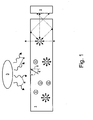
- Figure 1 schematically depicts a quantum dot solar concentrator.
- Figure 2 schematically illustrates a waveguide in which the core comprises substantially nonrandomly oriented nanowires.
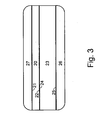
- Figure 3 schematically depicts a waveguide comprising a first core and a first layer in contact with each other. This embodiment is provided for comparative purposes.
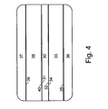
- Figure 4 schematically depicts a waveguide comprising a first layer in contact with two cores. This embodiment is provided for comparative purposes.
- Figure 5 schematically depicts a waveguide comprising a first, a second, and a third layer and two cores. This embodiment is provided for comparative purposes.
- Figure 6 illustrates absorption and emission by the organic dye fluorescein ( Panel A ) and by spherical CdSe nanocrystals with an aspect ratio of about 1.1 and an average diameter of about 2.3 nm ( Panel B ).
- Figure 7 depicts examples of vinyl-terminated polydimethylsiloxane oligomers ( Panel A ) and siloxane cross-linkers ( Panel B ) and illustrates the formation of cross-links between them ( Panel C ).
- Figure 8 schematically depicts examples of type II ( Panels A and C ) and type I ( Panels B and D ) band offsets.
- Nanocomposites Composite materials comprising nanostructures (nanocomposites) are provided, along with articles comprising nanocomposites and methods and compositions for making such composites.
- One class of embodiments provides light concentrators comprising nanostructures, This class of embodiments is based on the ability of certain nanostructures (e.g., nanostructures comprising a fluorescent material) to absorb and re-emit light that can then be waveguided by total internal reflection within at least one core.
- the nanostructures are provided in the form of a nanocomposite.
- the nanostructures are substantially nonrandomly oriented to increase the efficiency of the light concentrator.
- one aspect of the invention provides nanocomposites in which the matrix is used to orient nanowires.
- One aspect of the present invention provides light concentrators (e.g., solar concentrators) comprising nanostructures.
- Energy e.g., light
- the nanostructures are provided in the form of a nanocomposite.
- the average emission profile of all of the dye molecules looks isotropic.
- a few emitted light rays are indicated by solid arrows; continuing paths for some of these emitted rays are indicated by dashed arrows.
- Light that is re-emitted at angles that are greater than the critical angle for the interface between the sheet and the surrounding air is waveguided by total internal reflection and travels to the edge of the sheet before it escapes.
- light emitted at angles greater than the critical angle can be collected at the edge by a solar cell 2.
- C the ratio of light concentration collected
- S the ratio of the surface area of the sheet being illuminated by impinging light to the area of the collector at the edge of the sheet
- G represents losses in the concentrator that affect the ratio of the photons striking the surface of the concentrator to the number of photons that get guided to the edge of the sheet.
- G represents losses in the concentrator that affect the ratio of the photons striking the surface of the concentrator to the number of photons that get guided to the edge of the sheet.
- G losses in the concentrator that affect the ratio of the photons striking the surface of the
- dye molecules emit with finite quantum efficiency. As a result, even the photons that are absorbed do not all get re-emitted. Third, dye molecules are photo-unstable and eventually the concentrator stops working as the dye photobleaches. Finally, of the photons that are re-emitted, only those that emit at angles greater than the critical angle actually get wave guided and eventually collected. All other photons are lost. Other factors such as losses due to reabsorption or scatter within the concentrator also affect G, however, the factors above represent the major contributors to loss in this type of concentrator. As a result of these issues, solar concentrators of this type have not been implemented in a commercial product to date.
- Quantum dots have a number of substantial advantages over dye molecules: 1) they are extremely photostable and do not bleach, even under solar radiation; 2) they have an extremely broad absorption spectrum with extinction coefficients as much as 10 times greater than typical organic dye molecules and therefore absorb solar radiation much more efficiently than dye molecules; and 3) they can be fabricated with quantum efficiencies as high as 80%.
- quantum dots in a solar concentrator therefore improves performance of the concentrator by improving the first four contributions to G described above (absorption efficiency, absorption bandwidth, quantum yield, and photostability).
- the collection of quantum dots emits isotropically and thus their use does not increase the percentage of emitted photons that are waveguided (the fifth contribution to G).
- a quantum dot concentrator having quantum dots embedded in a transparent sheet surrounded by air, where the collection of dots emits light isotropically, at most 1 ⁇ 2*(cos(arcsin(n 1 /n 2 ))-cos(pi-arcsin(n 1 /n 2 ))) of the light emitted by the quantum dots can be waveguided and thus collected, where n 1 is the refractive index of air and n 2 is the refractive index of the sheet, cos is cosine, arcsin is arcsine, and pi is the Greek letter approximately equal to 3.14159265.
- the light concentrators of this invention comprise at least one core, at least one adjacent material that has a lower index of refraction than the core and that is in contact with at least a portion of a surface of the core, and a plurality of nanostructures.
- the nanostructures absorb light that impinges on a surface of the concentrator and re-emit light.
- the location of the nanostructures within the concentrator and/or the orientation of the nanostructures is controlled such that the fraction of the light emitted by the nanostructures that is waveguided by the core or cores is greater than 1 ⁇ 2*(cos(arcsin(n 1 /n 2 ))-cos(pi-arcsin(n 1 /n 2 ))), where n 1 is the refractive index of the adjacent material and n 2 is the refractive index of the core.
- At least 1%, more preferably at least 10%, or most preferably at least 50% of the total nanostructures in the concentrator are located or oriented such that greater than 1 ⁇ 2*(cos(arcsin(n 1 /n 2 ))-cos(pi-arcsin(n 1 /n 2 ))), where n 1 is the refractive index of the adjacent material and n 2 is the refractive index of the core, of the light emitted by the nanostructures is waveguided by the core(s).
- At least one collector for collecting the waveguided light is operably connected to the core, e.g., to an edge of the core.
- Any type of collector can be used for collecting the light and/or measuring its intensity, for example, a detector, fiber optic cable, photocell, or solar cell.
- any edges or portions of an edge of the core not occupied by the collector can be mirrored or silvered, so the waveguided light does not escape through these regions and decrease the efficiency of the concentrator.
- the adjacent material can be e.g., a cladding, a first layer comprising the nanostructures, or a layer of any low refractive index material.
- the location of the nanostructures within the concentrator can be controlled.
- the nanostructures can be located within the core or as a comparative example, they can be outside the core, e.g., in the material adjacent to the core.
- the orientation of the nanostructures can be controlled.
- the light concentrator can comprise any nanostructures that have a definable unique axis of symmetry (e.g. a unique crystal axis such as the c-axis of a wurtzite nanocrystal, the elongated axis of a nanowire, or the long axis along the arm of a nanotetrapod).
- Placement of such nanostructures with a substantially non-random distribution of orientations of the unique axis e.g., relative to a surface of the concentrator or each other, can increase the amount of light collected by the concentrator.
- a vector average of the orientation of the nanostructures' unique axis can have a nonzero component perpendicular to a surface of the concentrator.
- a plurality of substantially spherical nanocrystals (having an aspect ratio between about 0.8 and about 1.2) that have a wurtzite crystal structure can have a substantially non-random distribution of the c-axis of each wurtzite crystal and thus increase the percentage of light that is reemitted at angles greater than the critical angle, e.g. for a particular core-cladding combination.
- the light concentrator comprises at least one core, a cladding having a lower index of refraction than the core, and a plurality of nanowires that are located inside the core.
- the nanowires inside the core are substantially nonrandomly oriented in such a manner that, if a three-dimensional rectangular coordinate system is imposed on the core and the position of each nanowire is represented by a vector of unit length, the vector average of the nanowires' orientations has a nonzero component perpendicular to a surface of the core.
- Nanowires absorb light isotropically, but, unlike quantum dots, they re-emit light in a non-isotropic pattern defined by a radiating dipole oriented along the long axis of the nanowire. As a result, most of the fluorescence for a given nanowire is emitted in a direction perpendicular to the long axis of the nanowire. This is different than the case for fluorescent dye molecules and for quantum dots, which is one of the reasons why the present invention is so unique. In the case of dye molecules, while emission from a single molecule is non-isotropic, defined by a radiating dipole, the absorption is also non-isotropic, with an absorption dipole typically oriented substantially parallel (but not always exactly parallel) to the emission dipole.
- Quantum dots on the other hand, have isotropic absorption and emission (or isotropic absorption and 2-dimensional emission). In both of these cases, there is very inefficient light collection by the concentrator.
- the molecules that absorb light are those whose excitation dipole are oriented more parallel to the waveguide surface than perpendicular. These molecules, which typically have an emission dipole that is oriented in substantially the same direction as the excitation dipole, will then re-emit more strongly in a direction perpendicular to the waveguide than parallel. As a result, the light is not efficiently waveguided.
- quantum dots In the case of quantum dots, all quantum dots absorb light, but there is no orientation that directs light efficiently parallel to the waveguide (at best, one of the two dipoles in the 2D transition dipole will be oriented to emit within the plane while the other emits out of the plane. As a result, efficient collection is not achieved.
- nanowires in a collection of nanowires are randomly oriented, emission by the collection of nanowires is isotropic, but if the nanowires are nonrandomly oriented, emission by the collection is non-isotropic.
- the greater the percentage of nanowires that have a component of their long axis oriented perpendicular to the surface of the core is, or the greater the component of the vector average of the nanowires' orientations perpendicular to the surface is, the greater the percentage of light reemitted at angles greater than the critical angle and thus waveguided by the core is.
- At least 1%, more preferably at least 10%, or most preferably at least 50% of all the nanowires within the core are substantially nonrandomly oriented, in a direction perpendicular to the surface of the core.
- at least one collector for collecting the waveguided light e.g., a detector, fiber optic cable, photocell, or solar cell
- the core e.g., to at least one edge of the core.
- the light concentrator comprises at least one core and a first layer comprising one or more nanostructures disposed on a surface of the core.
- the nanostructures absorb light that impinges on a surface of the concentrator and re-emit light, and greater than 1 ⁇ 2*(cos(arcsin(n 1 /n 2 ))-cos(pi-arcsin(n 1 /n 2 ))), where n 1 is the refractive index of the first layer and n 2 is the refractive index of the core, of the re-emitted light is waveguided by the core(s).
- a radiating dipole located on or near a dielectric interface emits most of its light into the higher index material.
- the light is emitted into the higher index material at angles greater than the critical angle for that interface.
- the dipole is oriented at an angle substantially normal to the dielectric interface, an even greater percentage of the light is emitted beyond the critical angle.
- the light concentrator comprises a first layer comprising a plurality of nanowires disposed on a surface of the core and substantially nonrandomly oriented such that a vector average of the nanowires' orientations has a nonzero component perpendicular to the surface of the core.
- a vector average of the nanowires' orientations has a nonzero component perpendicular to the surface of the core.
- at least 1%, more preferably at least 10%, and most preferably at least 50% of all the nanowires on the core are substantially nonrandomly oriented in this manner, since the greater the degree of orientation perpendicular to the surface of the core, the greater the efficiency of capture of the re-emitted light.
- the light concentrators or layers thereof can be e.g. either two dimensional or one dimensional.
- the core is substantially larger than necessary to support a single optical mode at the wavelength that is re-emitted by the nanostructures in the concentrator in more than one dimension.
- the core can support only a single mode in two of three dimensions.
- any other layers in the concentrator can be e.g. placed on a single surface or e.g. the layers can be created concentrically around a central layer (as is the case for an optical fiber).
- the central layer can be either the core or e.g. an adjacent material, a cladding, or a first layer. Remaining layers are then built from the inside out.
- One embodiment provides a waveguide that comprises a cladding and a core.
- the core comprises one or more nanowires, or one or more branched nanowires, and a matrix (the core comprises a nanocomposite).
- the first and second surfaces of the core are substantially parallel to each other, permitting the core to act as an efficient waveguide.
- the core has a higher index of refraction (refractive index) than the cladding, and is in contact with the cladding over at least a majority of its first and second surfaces.
- the cladding comprises a material that has a lower refractive index than the core, e.g., a lower refractive index solid, liquid, or gas, e.g., air, a low index plastic or polymer film or sheet, or any other convenient material having a smaller index of refraction than the core.
- a lower refractive index solid, liquid, or gas e.g., air, a low index plastic or polymer film or sheet, or any other convenient material having a smaller index of refraction than the core.
- the cladding need not be a single substance; the cladding in contact with the first surface of the core can comprise a different material than the cladding in contact with the second surface, for example.
- the refractive index of the core must be greater than that of the cladding.
- the core can have an index of refraction greater than about 1.35, greater than about 2.5, greater than about 3.3, or even greater than 4.
- the core has an index of refraction between about 1.35 and about 4.
- the matrix of the core is preferentially substantially nonabsorbing and nonscattering with respect to light at wavelengths absorbed and emitted by the nanowires or branched nanowires in the core.
- the matrix is preferably substantially nonabsorbing and nonscattering to light in the visible, near-infrared, and infrared range, and thus is preferably substantially nonabsorbing and nonscattering with respect to wavelengths greater than about 300 nm (e.g., greater than about 300 or 400 nm and less than about 10 or 20 micrometers).
- a physical property of the matrix such as e.g.
- the waveguide (and typically also the core) is a flat sheet, which can be of considerable size. (As will be evident, weaker materials can still be formed into large sheets, e.g. with the provision of suitable physical support.)
- the matrix can comprise e.g. a glass, a polymer, an organic polymer, an inorganic polymer, an organometallic polymer, a small molecule or molecular matrix, a gel, a liquid, a crystal, a polycrystal, or a mesoporous matrix; a number of these are known (e.g., the example polymers, glasses, and small molecules mentioned and/or referenced herein).
- Example materials include but are not limited to acrylic and poly(methyl methacrylate); a large number of other suitable materials are known in the art.
- Either nanowires or branched nanowires (or a mixture thereof) can be used in the core.
- the branched nanowires can be nanotetrapods, or alternatively can be other branched structures (e.g., tripods or bipods).
- the diameter of the nanowires can be varied, for example, to control the wavelengths emitted by the nanowires.
- the waveguides comprise nanowires having an average diameter between about 2 nm and about 100 nm (e.g., between about 2 nm and about 50 nm, or between about 2 nm and about 20 nm). Nanowires with shorter aspect ratios are typically preferred, so in some embodiments the nanowires have an aspect ratio between about 1.5 and about 100, e.g. between about 5 and about 30.
- the waveguide core comprises a plurality of nanowires, which can be either randomly or substantially nonrandomly oriented.
- the orientation of the nanowires is substantially nonrandom, with the vector average of the nanowires' orientations having a nonzero component perpendicular to the first surface of the core.
- Preferably at least 1%, more preferably at least 10%, and most preferably at least 50% of all the nanowires in the core are substantially nonrandomly oriented in this manner, since the greater the degree of orientation perpendicular to the surface of the core, the greater the efficiency of capture of the re-emitted light.
- a majority of the nanowires each has its long axis oriented more nearly perpendicular to than parallel to a surface of the core.
- the nanowires within the core form a liquid crystal phase, in which each nanowire has its long axis oriented substantially perpendicular to a surface of the core. The use of such a liquid crystal phase results in a material that absorbs light from substantially all directions strongly but emits light primarily at angles inside the plane of the array.
- Figure 2 illustrates an example of a waveguide in which the core 10 comprises substantially nonrandomly oriented nanowires (9, cylinders).
- the nanowires absorb light (14, squiggly arrows) impinging on the waveguide from a light source 13 and re-emit light.
- a few rays of re-emitted light are indicated by solid arrows; continuing paths for some of these emitted rays are indicated by dashed arrows.
- Light that is re-emitted at angles that are greater than the critical angle 6 for the interface between the core and the cladding 12 is waveguided by total internal reflection and travels to the edge of the core before it escapes.
- ⁇ crit sin -1 (n r /n i ), where n r is the refractive index of the cladding and n i is the refractive index of the core.
- the waveguide core comprises a plurality of nanowires that absorb light impinging on a surface of the core and emit light.
- the nanowires are oriented in the core in such a manner that a majority of the emitted light is emitted an angle greater than the critical angle for the specific core-cladding combination. A majority of the emitted light is thus waveguided and directed toward at least one edge of the core.
- This type of waveguide can be an efficient light concentrator, since the waveguide can absorb light over a large surface area and direct it to an edge which has a much smaller area.
- the one or more nanowires or branched nanowires can be fabricated from essentially any convenient material.
- the nanowires or branched nanowires can comprise a semiconducting material, for example a material comprising a first element selected from group 2 or from group 12 of the periodic table and a second element selected from group 16 (e.g., ZnS, ZnSe, ZnTe, CdS, CdSe, CdTe, HgS, HgSe, HgTe, MgS, MgSe, MgTe, CaS, CaSe, CaTe, SrS, SrSe, SrTe, BaS, BaSe, BaTe, and like materials); a material comprising a first element selected from group 13 and a second element selected from group 15 (e.g., GaN, GaP, GaAs, GaSb, InN, InP, InAs, InSb, and like materials); a material comprising a group14 element (G
- the nanowires or branched nanowires preferably comprise a fluorescent material, more preferably one with a high quantum yield (e.g., a quantum yield greater than about 5%, 10%, 20%, 50%, or 75%).
- the nanowires or branched nanowires can comprise one or more materials having a band-gap energy between about 0.4 eV and about 4.1 eV.
- Each nanowire or branched nanowire can comprise a single material or can be a heterostructure comprising at least two different and/or distinguishable materials.
- the two or more materials can be entirely different (e.g., can have different chemical compositions), or they can comprise the same base material but have different dopants or different concentrations of the same dopant.
- the different materials can be distributed at different locations along the long axis of the nanowire or along the long axis of an arm of the branched nanowire, or different arms of the branched nanowire can comprise different materials.
- the heterostructures can be core-shell heterostructures, in which a nanowire or branched nanowire comprises a core of a first material and at least one shell of a second (or third etc.) material, where the materials are distributed radially about the long axis of the nanowire or the long axis of an arm of the branched nanowire.
- Suitable materials for a fluorescence efficiency-enhancing shell include e.g. materials having a higher band gap energy than the material forming the nanostructure's core.
- suitable materials for the shell can have e.g. good conduction and valence band offset with respect to the core material.
- the conduction band is preferably higher and the valence band is preferably lower than those of the core material.
- cores that emit energy in the visible range e.g., CdS, CdSe, CdTe, ZnSe, ZnTe, GaP, GaAs
- near-infrared e.g., InP, InAs, InSb, PbS, PbSe
- a material that has a band gap energy e.g. in the ultraviolet range can be used (e.g., ZnS, GaN, and magnesium chalcogenides, e.g., MgS, MgSe, and MgTe).
- materials having a band gap energy e.g. in the visible range e.g. CdS or CdSe
- At least one collector for collecting the waveguided light e.g., a detector, fiber optic cable, photocell, or solar cell
- a collector for collecting the waveguided light is optionally operably connected to at least one edge of the core.
- any edges or portions of an edge of the core not occupied by the collector can be mirrored or silvered.
- any of the embodiments described above can be used to form multilayer tandem light concentrators, in which different wavelengths (or different single bands of wavelengths) are collected in different layers and waveguided, e.g., to photocells or solar cells optimized for these specific wavelengths.
- one layer can concentrate near ultraviolet-low wavelength visible light
- another layer can concentrate visible-near infrared light
- a third layer can concentrate near infrared-infrared light.
- Such a multilayer light concentrator comprises a stack of two or more waveguides as described above.
- the order of the waveguides within the stack is preferably such that the waveguide comprising the nanowires or branched nanowires absorbing the shortest wavelength light (having the highest band-gap) is located closest to the light source (e.g., the sun) and the waveguide comprising the nanowires or branched nanowires absorbing the longest wavelength light (having the smallest band-gap) is located farthest from the light source.
- a radiating dipole located on or near a dielectric interface emits most of its light into the higher index material at angles greater than the critical angle for that interface. Additionally, if the dipole is oriented at an angle substantially normal to the dielectric interface, an even greater percentage of the light is emitted beyond the critical angle.
- This class of embodiments provides a waveguide that comprises a cladding, a first core, and a first layer comprising one or more nanostructures.
- the one or more nanostructures can be nanowires, branched nanowires (e.g., nanotetrapods, tripods, or bipods), or nanocrystals.
- the first and second surfaces of the first core are substantially parallel to each other, permitting the core to act as an efficient waveguide.
- the first layer is distributed on the first surface of the first core, but the core and the layer are not necessarily in contact with each other.
- the cladding has a first portion distributed on the second surface of the first core and a second portion distributed on the first surface of the first layer, but the cladding is not necessarily in direct contact with these surfaces.
- the second portion of cladding 27 is in contact with at least a majority of first surface 21 of first layer 20, second surface 22 of the first layer is in contact with at least a majority of first surface 24 of first core 23, and at least a majority of second surface 25 of the first core is in contact with first portion of cladding 26.
- the cladding typically has a refractive index less than the refractive index of the core.
- the one or more nanostructures absorb light impinging on the top or bottom surface of the waveguide and emit light, and a majority of the emitted light is emitted into the first core at an angle greater than the critical angle for the specific core-first layer combination.
- a majority of the emitted light is thus waveguided and directed toward at least one edge of the core.
- This type of waveguide can be an efficient light concentrator, since the waveguide can absorb light essentially isotropically over a large surface area and direct it to an edge which has a much smaller area.
- the first layer and the first core can be separated, e.g., by a layer of a material having a refractive index between that of the first layer and first core.
- the waveguide further comprises a second core.
- the second core has two substantially parallel surfaces and is located between, but is not necessarily in contact with, the first layer and the second portion of the cladding.
- the first and second cores comprise the same material, although they can be formed of different materials.
- the second portion of the cladding 37 is in contact with the top surface 39 of the second core 38
- the bottom surface 40 of the second core is in contact with the first surface 31 of the first layer
- the second surface 32 of the first layer is in contact with the first surface 34 of the first core 33
- the second surface 35 of the first core is in contact with the first portion of the cladding 36.
- the first layer and the cladding portions each have a refractive index less than that of the first and second cores.
- a waveguide comprising a second core further comprises a second layer located between the second core and the first layer and a third layer located between the first layer and the first core.
- the second and third layers each have an index of refraction that is greater than the refractive index of the first layer but less than the refractive index of the first and second cores.
- the second layer 51 is typically in contact with the second core 53 and the first layer 50
- the third layer 52 is typically in contact with the first layer 50 and the first core 54.
- the cladding portions 55 (shown in contact with the second core 53) and 56 (shown in contact with the first core 54) preferably have an index of refraction less than that of the first and second cores.
- the second and third layers can be the same or different materials, and preferably are formed from a material that is substantially nonabsorbing and scattering at the relevant wavelengths (e.g., greater than about 300 nm, or between about 300 or 400 nm and about 10 or 20 micrometers).
- the first layer is typically a thin layer having a high concentration of nanostructures. The high concentration of nanostructures in the first layer permits efficient absorption of light, which is re-emitted primarily into the surrounding second and third layers and then passes into the cores. Removal of the light from the nanostructure layer reduces losses from scattering and reabsorption of the emitted light by the nanostructures.
- the first layer can consist e.g., of a plurality of substantially pure nanostructures, e.g., nanostructures without a surrounding matrix.
- a layer can be formed, for example, by spin-casting or otherwise depositing a solution of nanostructures in a solvent on the surface of a core or other layer and then evaporating the solvent.
- the first layer can comprise e.g., one or more nanostructures in a matrix (the first layer can be a nanocomposite).
- Preferred matrices have a relatively low index of refraction, since the first layer preferably has a refractive index that is less than that of the first (and second, if present) core.
- the matrix can be, for example, a small molecule or molecular matrix or a matrix comprising at least one polymer or glass.
- a number of small molecules, glasses, and polymers e.g., organic, inorganic, and organometallic polymers are known in the art (e.g., those mentioned and/or referenced herein).
- the first layer comprises one or more nanostructures in a matrix comprising a polysiloxane, preferably polydimethylsiloxane (PDMS).
- the matrix comprises an inorganic glassy material such as SiO 2 or TiO 2 .
- the nanostructures can but need not be dispersed uniformly throughout the first layer, e.g., the nanostructures can be located primarily in a portion of the first layer that is adjacent to one of the cores.
- the cladding comprises a material that has a lower refractive index than the core, e.g., a lower refractive index solid, liquid, or gas, e.g., air, a low index plastic or polymer film or sheet, or any other convenient material having a smaller index of refraction than the core.
- the first and second portions of the cladding need not comprise the same material.
- the first core is preferentially substantially nonabsorbing and nonscattering with respect to relevant wavelengths (including, for example, those wavelengths emitted by the nanowires or branched nanowires distributed on the core).
- the first core is preferably substantially nonabsorbing and nonscattering to light in the visible, near-infrared, and infrared range, and thus is preferably substantially nonabsorbing and nonscattering with respect to wavelengths greater than about 300 nm (e.g., greater than about 300 or 400 nm and less than about 10 or 20 micrometers).
- the first core can have an index of refraction greater than about 1.35, greater than about 2.5, greater than about 3.3, or even greater than 4.
- the first core has an index of refraction between about 1.35 and about 4.
- a physical property of the first core such as e.g. its mechanical strength can be another criterion used to select an appropriate core material, since in some embodiments the waveguide (and typically also the core) is a flat sheet, which can be of considerable size. (As will be evident, weaker materials can still be formed into large sheets, e.g. with the provision of suitable physical support.) Similar considerations apply to the second core.
- the first (or second) core can comprise e.g. a glass, a polymer, an organic polymer, an inorganic polymer, an organometallic polymer, a small molecule or molecular matrix, a gel, a liquid, a crystal, a polycrystal, or a mesoporous matrix; a number of these are known (e.g., the example polymers and small molecules mentioned and/or referenced herein).
- Example materials for the first (or second) core include but are not limited to acrylic and poly(methyl methacrylate); a large number of other suitable materials are known in the art.
- the first layer is preferably substantially nonscattering with respect to light at relevant wavelengths (e.g., the wavelengths absorbed and emitted by the nanostructures).
- relevant wavelengths e.g., the wavelengths absorbed and emitted by the nanostructures.
- the first layer is preferably substantially nonscattering to light in the visible, near-infrared, and infrared range, and thus is preferably substantially nonscattering with respect to wavelengths greater than about 300 nm (e.g., greater than about 300 or 400 nm and less than about 10 or 20 micrometers).
- the first layer is also preferably substantially nonabsorbing with respect to the wavelength or wavelengths of light emitted by the nanostructures in the layer.
- the first layer has a thickness less than about one wavelength of the light emitted by the one or more nanostructures.
- the first layer can have a thickness less than about 1000 nm (e.g., for near-infrared light), less than about 900 nm, less than about 800 nm, less than about 700 nm, less than about 600 nm, less than about 500 nm (e.g., for green light), or less than about 400 nm.
- the thickness of the first layer affects the efficiency of the waveguide because the effect on which this class of embodiments is based, the emission of light by a radiating dipole into the higher index material at a dielectric interface, decreases as the dipole is moved away from the interface and has no effect beyond the distance of about one wavelength of the light emitted. In most cases, a layer substantially thinner than this can be used to absorb substantially all the incident light, so this does not result in a performance limitation.
- the first layer can comprise one or more nanostructures (e.g., nanowires, branched nanowires, or nanocrystals), or a plurality of nanostructures.
- the one or more nanostructures can be fabricated from essentially any convenient materials.
- the nanostructures can comprise a semiconducting material, for example a material comprising a first element selected from group 2 or from group 12 of the periodic table and a second element selected from group 16 (e.g., ZnS, ZnSe, ZnTe, CdS, CdSe, CdTe, HgS, HgSe, HgTe, MgS, MgSe, MgTe, CaS, CaSe, CaTe, SrS, SrSe, SrTe, BaS, BaSe, BaTe, and like materials); a material comprising a first element selected from group 13 and a second element selected from group 15 (e.g., GaN, GaP, GaAs, Ga
- the nanostructures preferably comprise a fluorescent material, more preferably one with a high quantum yield (e.g., a quantum yield greater than about 5%, 10%, 20%, 50%, or 75%).
- the nanostructures can comprise one or more materials having a band-gap energy between about 0.4 eV and about 4.1 eV.
- Each nanostructure can comprise a single material or can be a heterostructure comprising at least two different and/or distinguishable materials.
- the two or more materials can be entirely different (e.g., can have different chemical compositions), or they can comprise the same base material but have different dopants or different concentrations of the same dopant.
- the heterostructures can be core-shell heterostructures, in which a nanowire, branched nanowire, or nanocrystal comprises a core of a first material and at least one shell of a second (or third etc.) material, where the materials are distributed radially about the long axis of the nanowire, the long axis of an arm of the branched nanowire, or the center of the nanocrystal.
- Suitable materials for a fluorescence efficiency-enhancing shell include e.g. materials having a higher band gap energy than the material forming the nanostructure's core.
- suitable materials for the shell can have e.g. good conduction and valence band offset with respect to the core material. That is, the conduction band is preferably higher and the valence band is preferably lower than those of the core material.
- a material that has a band gap energy e.g. in the ultraviolet range can be used (e.g., ZnS, GaN, and magnesium chalcogenides, e.g., MgS, MgSe, and MgTe).
- materials having a band gap energy e.g. in the visible range e.g., CdS, CdSe, CdTe, ZnSe, ZnTe, GaP, GaAs
- a material that has a band gap energy e.g. in the ultraviolet range can be used (e.g., ZnS, GaN, and magnesium chalcogenides, e.g., MgS, MgSe, and MgTe).
- materials having a band gap energy e.g. in the visible range e.g.
- the different materials can be distributed at different locations within the nanostructure.
- the different materials can be at different locations along the long axis of a nanowire or along the long axis of an arm of a branched nanowire, or different arms of a branched nanowire can comprise different materials.
- the size of the nanostructures can be varied; for example, to control the wavelengths emitted by the nanostructures.
- the waveguides comprise nanowires having an average diameter between about 2 nm and about 100 nm (e.g., between about 2 nm and about 50 nm, or between about 2 nm and about 20 nm).
- nanowires with shorter aspect ratios are preferred; thus, in some embodiments the nanowires preferably have an aspect ratio between about 1.5 and about 100, e.g. between about 5 and about 30.
- the waveguides comprise nanocrystals having an average diameter between about 1.5 nm and about 15 nm (e.g., between about 2 nm and about 5 nm, between about 5 nm and about 10 nm, or between about 10 nm and about 15 nm).
- the nanocrystals typically have an aspect ratio between about 0.1 and about 1.5, e.g., between about 0.5 and about 1.5, preferably between about 1 and about 1.5.
- the first layer comprises a plurality of nanowires, which can be either randomly or substantially nonrandomly oriented.
- the orientation of the nanowires is substantially nonrandom, with the vector average of the nanowires' orientations having a nonzero component perpendicular to a surface of the first core.
- Preferably at least 1%, more preferably at least 10%, and most preferably at least 50% of all the nanowires in the first layer are substantially nonrandomly oriented in this manner, since the greater the degree of orientation perpendicular to the surface of the core, the greater the efficiency of capture of the re-emitted light.
- a majority of the nanowires each has its long axis oriented more nearly perpendicular to than parallel to a surface of the first core.
- the nanowires within the first layer form a liquid crystal phase, in which each nanowire has its long axis oriented substantially perpendicular to a surface of the first core.
- the use of a liquid crystal phase results in a first layer that absorbs light from substantially all directions equally but emits light primarily into the adjacent higher index material at angles greater than the critical angle, providing a highly efficient light concentrator (as much as eight times more efficient than a similar concentrator where the nanowires are embedded inside the waveguide core).
- the first layer comprises a thin film comprising or consisting of nanocrystals.
- the nanocrystals emit more light into the adjacent higher index material (e.g., the core) at an angle greater than the critical angle, but the effect is not as pronounced as for a first layer comprising nanowires (particularly substantially nonrandomly oriented nanowires).
- a waveguide containing nanocrystals distributed on a core is, however, still more efficient than a waveguide containing quantum dots embedded in the core.
- the nanocrystals have a unique crystal axis
- efficiency can be increased by substantially nonrandomly orienting the nanocrystals such that a vector average of the nanocrystals orientations has a nonzero component perpendicular to a surface of the core.
- At least one collector for collecting the waveguided light is optionally operably connected to at least one edge of the first core.
- a second collector can optionally be connected to at least one edge of the second core.
- any edges or portions of an edge of the core or cores not occupied by the collector can be mirrored or silvered.
- any of the embodiments described above can be used to form multilayer tandem light concentrators, in which different wavelengths (or different single bands of wavelengths) are collected in different layers and waveguided, e.g., to photocells or solar cells optimized for these specific wavelengths.
- one layer can concentrate near ultraviolet-low wavelength visible light
- another layer can concentrate visible-near infrared light
- a third layer can concentrate near infrared-infrared light.
- Such a multilayer light concentrator comprises a stack of two or more waveguides as described above.
- the order of the waveguides within the stack is preferably such that the waveguide comprising the nanostructures absorbing the shortest wavelength light (having the highest band-gap) is located closest to the light source (e.g., the sun) and the waveguide comprising the nanostructures absorbing the longest wavelength light (having the smallest band-gap) is located farthest from the light source.
- a multi-layer concentrator can be fabricated such that it is symmetrically structured with the lowest energy bandgap waveguide in the center of the stack and increasing bandgap energies as the waveguide layers extend above and below the center layer(s).
- light can impinge on the stack from either side with equal efficiency.
- a multilayer light concentrator can also be assembled as a stack of waveguides in which at least one waveguide comprises nanowires within the core and at least one waveguide comprises nanostructures distributed on the core (each waveguide can include any of the variations described above).
- the nanostructures typically absorb light over a broad spectral range, e.g. compared to a dye molecule with emission at comparable wavelengths.
- the wavelength range over which light is absorbed can also be e.g. substantially broader than the range over which light is emitted.
- a nanostructure can emit light over a narrow spectral range, e.g., less than about 60 nm, preferably less than about 40 nm or about 30 nm.
- absorption typically increases in strength the farther in energy the light is from the emission wavelength (at shorter wavelengths only).
- a nanorod with emission at 700nm can absorb 300nm light more strongly than 400nm light, which can be more strongly absorbed than 500nm light, which can be more strongly absorbed than 600nm light. This is very different than what is observed for dye molecules, e.g. in a solar concentrator.
- the absorption peaks at an energy very close to the emission energy and then decreases quickly. As a result, conversion of light impinging on a dye molecule solar concentrator is very inefficient, since most of the wavelengths are not strongly absorbed.
- Figure 6 depicts examples of absorption and emission spectra for a dye and a nanostructure.
- Panel A depicts absorption (61) and emission (62) by the organic dye fluorescein.
- Panel B depicts absorption (63) and emission (64) by spherical CdSe nanocrystals with an aspect ratio of about 1.1 and an average diameter of about 2.3 nm.
- Other dyes and nanostructures have spectra with comparable features, e.g., generally comparable shape.
- Substantially nonrandom orientation of nanostructures is frequently desirable, e.g., within a composite material.
- waveguides and light concentrators comprising nonrandomly oriented nanostructures can be more efficient than similar waveguides or concentrators comprising randomly oriented nanostructures.
- One aspect of the present invention provides a composite material comprising a plurality of nanowires and a small molecule or molecular matrix or a matrix comprising at least one polymer, where the matrix (or the components and/or precursors of the matrix) is used to orient the nanowires (to produce a substantially nonrandom distribution of nanowire orientations).
- the nanowires can be fabricated of essentially any convenient material (e.g., a semiconducting material, a ferroelectric material, a metal, etc.) and can comprise essentially a single material or can be heterostructures.
- the matrix comprises a polymer that exhibits a liquid crystal phase.
- a combination of polymer and nanowires is selected, such that the mixture also exhibits a liquid crystal phase.
- a solution of nanowires (e.g., at a high concentration of nanowires) and polymer can be mixed together and placed in a small electric field to orient them in the desired direction.
- the polymer and the nanowires have comparable lengths; therefore, shorter nanowires are preferred (e.g., nanowires having lengths less than about 100 nm, less than about 50 nm, or less than about 20 nm).
- Liquid crystal polymers include, e.g., poly(m-phenylene isophthalamide), poly(p-benzamide), poly(alkyl isonitriles), polyisocyanates, and a number of other polymers, see e.g., Dietrich Demus, John W. Goodby, George W. Gray, Hans W. Spiess, and Volkmar Vill (1998) Handbook of Liquid Crystals, Handbook of Liquid Crystals : Four Volume Set, John Wiley and Sons, Inc .
- a liquid crystalline polymer or other polymeric or small molecule or molecular matrix can be used orient nanowires.
- Other methods for orienting nanowires are known to those of skill in the art.
- Liquid crystal phases of nanowires e.g., nanorods
- Nanorods aligned along the stretching direction in stretched polymer films are described in e.g. Peng et al (2000) “Shape control of CdSe nanocrystals” Nature 404: 59-61 .
- aligned nanowires can be grown substantially in situ as a field of oriented structures that are subsequently integrated into the polymer matrix. Methods of fabricating such fields of aligned nanostructures are described, e.g., in Published U.S. Patent Application Nos. 2002/0172820 and 2002/0130311 . Methods of orienting nanowires also include electric field assisted orientation of nanowires (e.g., nanorods), e.g., applying an electric field to cause magnetic nanorods to orient in a desired direction, in a polymer matrix which optionally can be hardened to maintain the orientation.
- electric field assisted orientation of nanowires e.g., nanorods
- Nanostructures can also be oriented to some degree. See e.g., Alivisatos (2000) "Naturally Aligned Nanocrystals" Science, 289, 736 .
- nanotetrapods can be self-orienting. When deposited on a surface, the nanotetrapods typically contact the surface via three arms; the fourth arm is perpendicular to the surface.
- nanocrystals will spontaneously align with their unique crystal axis oriented vertically when they are packed at high density on a surface.
- such nanocrystals are substantially faceted in shape such that the lowest energy packing state is one in which the non-symmetric unique axis of every nanocrystal is oriented vertically.
- the extent to which the nanostructures in a collection of nanostructures are ordered or nonrandomly oriented can be determined through various methods. For example, electron microscopy (e.g., SEM, TEM), atomic force microscopy (AFM), or scanning tunneling microscopy (STM) can readily be performed, e.g., on cross-sections of a nanocomposite material.
- electron microscopy e.g., SEM, TEM
- AFM atomic force microscopy
- STM scanning tunneling microscopy
- optical microscopy such as polarization or DIC microscopy can be used to determine the average orientation of nanowires or nanocrystals within a material.
- Electrostatic force microscopy can also be used in some cases to determine orientation due to an intrinsic dipole in many nanocrystals and nanowires oriented along their unique crystal axis.
- One aspect of the invention provides a composite material comprising one or more nanostructures and a polymeric matrix comprising a polysiloxane (e.g., a composite material comprising one or more nanostructures and a polymeric matrix consisting of a polysiloxane).
- a polysiloxane is an inorganic polymer whose backbone comprises alternating silicon and oxygen atoms; each silicon has two side groups. These groups can be e.g., a hydrogen atom, any organic group, or any alkyl group.
- Example polysiloxanes include but are not limited to polydimethylsiloxane (PDMS), polymethylphenylsiloxane, polydiphenylsiloxane, and polydiethylsiloxane.
- a polysiloxane can also be a copolymer comprising at least two different types of siloxane monomers, e.g., dimethylsiloxane and methylhydrogensiloxane (in which one of the side groups is a methyl group and the other side group is a hydrogen).
- the composite comprises one or more nanostructures in a matrix comprising polydimethylsiloxane (PDMS) or in a matrix comprising a copolymer between dimethylsiloxane and another siloxane (e.g., methylhydrogensiloxane).
- the polysiloxane matrix can comprise e.g. linear or cross-linked polysiloxane oligomers.
- the matrix can be e.g. substantially free of silicates.
- the polymeric matrix is distinct from ORMOSIL (organically modified silicate) matrices.
- kits comprising vinyl-terminated dimethylsiloxane oligomers ( Figure 7 , Panel A ), siloxane cross-linkers (polysiloxane oligomers where the monomers are usually dimethylsiloxane but occasionally methylhydrogensiloxane, Panel B ), and a catalyst (which catalyzes the addition of an SiH bond across a vinyl group to form an Si-CH 2 -CH 2 -Si linkage, as illustrated in Panel C ) are generally commercially available, e.g., from Dow Coming (SYLGARD 184 TM, www.dowcorning.com).
- the nanostructures can be e.g., nanowires, nanocrystals, branched nanowires (e.g., nanotetrapods, tripods, or bipods), nanoparticles, teardrops, or any other desired nanostructures.
- the nanostructures can be fabricated from essentially any convenient material.
- the nanostructures can comprise e.g. one or more metals (e.g., Au, Ag, Ni, Cu, Zn, or Pt), or an alloy or mixture thereof.
- the nanostructures can comprise e.g., a ferroelectric or ferroelectric ceramic material, including, for example, a perovskite-type material (including but not limited to BaTiO 3 , SrTiO 3 , CaTiO 3 , KNbO 3 , PbTiO 3 , LiTiO 3 , LiTaO 3 , or LiNbO 3 , or a material derived from these, for example, Ba( 1-x )Ca x TiO 3 where x is between 0 and 1, or PbTi( 1-x )Zr x O 3 where x is between 0 and 1); a KDP-type material (e.g., KH 2 PO 4 , KD 2 PO 4 , RbH 2 PO 4 , RbH 2 AsO 4 , KH 2 AsO 4 , or GeTe, or a material derived from these); a TGS-type material (e.g., tri-glycine sulfate,
- the nanostructures can comprise a semiconducting material, for example, a material comprising a first element selected from group 2 or from group 12 of the periodic table and a second element selected from group 16 (e.g., ZnS, ZnSe, ZnTe, CdS, CdSe, CdTe, HgS, HgSe, HgTe, MgS, MgSe, MgTe, CaS, CaSe, CaTe, SrS, SrSe, SrTe, BaS, BaSe, BaTe, and like materials); a material comprising a first element selected from group 13 and a second element selected from group 15 (e.g., GaN, GaP, GaAs, GaSb, InN, InP, InAs, InSb, and like materials); a material comprising a group14 element (Ge, Si, and like materials); a material such as PbS, PbSe, PbTe, AlS,
- the nanostructures preferably comprise a fluorescent material, more preferably one with a high quantum yield (e.g., a quantum yield greater than about 5%, 10%, 20%, 50%, or 75%).
- the nanostructures can comprise one or more materials having a band-gap energy between about 0.4 eV and about 4.1 eV.
- Each nanostructure can comprise a single material or can be a heterostructure comprising at least two different and/or distinguishable materials.
- the composite material can further comprise at least one surfactant or at least one solvent.
- the composite can comprise a surfactant used to assist in uniformly dispersing the nanostructures throughout the polysiloxane matrix.
- the surfactant can interact with the surface of the nanostructures and with the polysiloxane monomers or polymer.
- the surfactant can be attached to the surface of the nanostructures by ionic or covalent bonds, or other molecular forces and/or to the polymer by ionic or covalent bonds, or other molecular forces.
- the polysiloxane nanocomposite of this invention can be formed into a number of shaped articles.
- a light-emitting diode (LED), laser, waveguide (e.g., as described herein), or amplifier, for example, can comprise a polysiloxane-containing composite. See e.g. US 20010046244 entitled "Optical amplifiers and lasers" by Klimov et al.
- Such structures will be greatly improved by the inclusion of one or more nanostructures to provide additional optical, electronic, or other functionality to an otherwise passive material.
- polysiloxanes such as PDMS are useful in the formation of microfluidic devices.
- the composite of the present invention allows the incorporation of active optical components into such devices.
- One class of embodiments provides a composite material that comprises either a small molecule or molecular matrix or a matrix comprising at least one organic polymer or an inorganic glass and one or more branched nanowires or one or more inorganic nanowires (or a combination thereof).
- the inorganic nanowires have an aspect ratio greater than about 10 (e.g., greater than about 15, greater than about 20, or greater than about 50) and can be either semiconducting or ferroelectric.
- the branched nanowires can be nanotetrapods, for example, or can be other branched structures such as e.g. tripods or bipods.
- the composite comprises a plurality of inorganic nanowires, which can be either randomly or substantially nonrandomly oriented.
- the composite material is formed into a thin film within which the orientation of the inorganic nanowires is substantially nonrandom. For example, at least 1% (e.g., at least 10%, or at least 50%) of all the nanowires in the film can be substantially nonrandomly oriented.
- the thin film can be either substantially free of strain, or it can be highly strained (for example, if the nonrandom orientation of the nanowires is achieved by stretching the film).
- the composite is formed into a thin film within which a majority of the nanowires are oriented such that each nanowire has its long axis substantially parallel to a surface of the film.
- the composite is formed into a thin film within which a majority of the nanowires are oriented such that each nanowire has its long axis more nearly perpendicular than parallel to a surface of the film.
- the composite is formed into a thin film within which a majority of the nanowires are oriented such that each nanowire has its long axis substantially perpendicular to a surface of the film.
- the inorganic nanowires can be fabricated from a ferroelectric or ferroelectric ceramic material.
- the inorganic nanowires can comprise a perovskite-type material (including but not limited to BaTiO 3 , SrTiO 3 , CaTiO 3 , KNbO 3 , PbTiO 3 , LiTiO 3 , LiTaO 3 , or LiNbO 3 , or a material derived from these, for example, Ba (1-x) Ca x TiO 3 where x is between 0 and 1, or PbTi (1-x) Zr x O 3 where x is between 0 and 1); a KDP-type material (e.g., KH 2 PO 4 , KD 2 PO 4 , RbH 2 PO 4 , RbH 2 AsO 4 , KH 2 AsO 4 , or GeTe, or a material derived from these); a TGS-type material (e.g., tri-glycine sul
- the inorganic nanowires can be fabricated from a semiconducting material.
- the nanowires can comprise a material comprising a first element selected from group 2 or from group 12 of the periodic table and a second element selected from group 16 (e.g., ZnS, ZnSe, ZnTe, CdS, CdSe, CdTe, HgS, HgSe, HgTe, MgS, MgSe, MgTe, CaS, CaSe, CaTe, SrS, SrSe, SrTe, BaS, BaSe, BaTe, and like materials); a material comprising a first element selected from group 13 and a second element selected from group 15 (e.g., GaN, GaP, GaAs, GaSb, InN, InP, InAs, InSb, and like materials); a material comprising a group14 element (Ge, Si, and like materials); a material such as PbS, Pb
- the branched nanowires can be fabricated from essentially any convenient material.
- the branched nanowires can comprise a metal (e.g., Ag, Au, Ni, Cu, Zn, or Pt) or a ferroelectric or semiconducting material (e.g., those listed in previous section).
- the composite comprises a small molecule or molecular matrix.
- matrices are known in the art, comprising e.g., molecular organics such as those used in OLEDs; N,N'-diphenyl-N,N'-bis (3-methylphenyl)-(1,1'biphenyl)-4,4'-diamine) (TPD); (3-(4-biphenyl)-4-phenyl-5-tert-butylphenyl-1,2,4-triazole) (TAZ); tris-(8-hydroxyquinoline) aluminum (Alq 3 ); benzoic acid; phthalic acid; benzoin; hydroxyphenol; nitrophenol; chlorophenol; chloroaniline; or chlorobenzoamide.
- Preferred small molecules have at least one polar functional group and have a high enough melting point that they are solid at room temperature.
- the matrix comprises an inorganic glass.
- Such glasses are known in the art, e.g., SiO 2 or TiO 2 .
- the composite comprises a matrix comprising at least one organic polymer.
- organic polymer A wide variety of such polymers is known to those of skill in the art (see e.g., Dietrich Demus, John W. Goodby, George W. Gray, Hans W. Spiess, and Volkmar ViII (1998) Handbook of Liquid Crystals, Handbook of Liquid Crystals: Four Volume Set, John Wiley and Sons, Inc .; Johannes Brandrup (1999) Polymer Handbook, John Wiley and Sons, Inc. ; and Charles A. Harper (2002) Handbook of Plastics, Elastomers, and Composites, 4th edition, McGraw-Hill ).
- thermoplastic polymers e.g., polyolefins, polyesters, polysilicones, polyacrylonitrile resins, polystyrene resins, polyvinyl chloride, polyvinylidene chloride, polyvinyl acetate, or fluoroplastics
- thermosetting polymers e.g., phenolic resins, urea resins, melamine resins, epoxy resins, polyurethane resins
- engineering plastics e.g., polyamides, polyacrylate resins, polyketones, polyimides, polysulfones, polycarbonates, polyacetals
- liquid crystal polymers including main chain liquid crystal polymers (e.g., poly(hydroxynapthoic acid)) and side chain liquid crystal polymers (e.g., poly ⁇ n-((4'(4"-cyanphenyl)phenoxy)alkyl)vinyl esther>).
- Certain embodiments include conductive organic polymers; see e.g. T. A. Skatherin (ed.) Handbook of Conducting Polymers I .
- Examples include but are not limited to poly(3-hexylthiophene) (P3HT), poly[2-methoxy, 5-(2'-ethylhexyloxy)-p-phenylene-vinylene] (MEH-PPV), poly(phenylene vinylene) (PPV), and polyaniline.
- the diameter of the inorganic nanowires can be varied, for example, to control the wavelength emitted by fluorescent nanowires.
- the diameter of the nanowires is preferably between about 2 nm and about 100 nm, more preferably between about 2 nm and about 5 nm or between about 10 nm and about 50 nm.
- the length of the nanowires can also be varied.
- the inorganic nanowires have an aspect ratio between about 10 and about 10,000 (e.g., between about 20 and about 10,000, between about 50 and about 10,000, or between about 100 and about 10,000).
- the composite materials comprising ferroelectric nanowires or ferroelectric branched nanowires have a number of uses.
- the nanocomposites can be used in data storage media, where information is encoded by flipping the ferroelectric state of individual nanowires or nanoparticles to write bits.
- the composite in embodiments where the composite has a high dielectric constant, can be used as an insulator (e.g., formed into thin insulating films such as those printed on circuit boards).
- the composite materials comprising semiconducting nanowires or semiconducting branched nanowires also have a number of uses.
- a composite comprising semiconducting nanowires or branched nanowires and e.g. a conductive polymer or small molecule or molecular matrix can be used in a photovoltaic device, where the nanowires conduct the electrons and the polymer or small molecule or molecular matrix is the hole-conducting element.
- At least one blocking layer is optionally used to restrict the movement of charges (e.g., to prevent the movement of electrons or holes in a particular direction, through a particular region of a device, or to a particular electrode).
- a blocking layer is a layer of some material either organic or inorganic, which has either: a high hole conductivity and high electron resistance to allow hole flow and prevent electron flow, or a high electron conductivity and high hole resistance to allow electron flow and prevent hole flow.
- Blocking layers can be incorporated e.g. onto either one or both sides of the active layer (e.g., a nanocomposite layer) of a photovoltaic device.
- the active layer e.g., a nanocomposite layer
- one or more blocking layers can be used to prevent a nanostructure photovoltaic cell from beginning to short out upon strong illumination and to assist in the creation of a high carrier density within nanostructures extending across the active layer.
- one or more blocking layers can be used to concentrate charges in an active region of a nanostructure-base LED to improve charge recombination within the nanocrystals.
- one aspect of the invention provides a composite material comprising a plurality of nanostructures and a small molecule or molecular matrix, a glassy or crystalline inorganic matrix, or a matrix comprising at least one polymer, where the composite is distributed on a first layer of a material that conducts substantially only electrons or substantially only holes.
- the composite and the first layer can be in contact with each other (e.g., over all or most of a surface of the first layer), or can be separated, for example, by a second layer comprising a conductive material.
- the second layer can conduct electrons, holes, or both.
- the first layer can be distributed on an electrode.
- the first layer can be in contact with the electrode (e.g., over all or most of a surface of the first layer), or can be separated, for example, by a layer of a nonconductive material or by a third layer comprising a conductive material.
- the third layer can conduct electrons, holes, or both.
- the nanostructures can be of any desired type (e.g., nanowires, branched nanowires, nanocrystals, or nanoparticles) and can be fabricated of essentially any convenient material (e.g., any metal or semiconducting or ferroelectric material such as those described herein), and can comprise a single material or can be heterostructures.
- the small molecule or molecular matrix can comprise e.g., molecular organics such as those used in OLEDs; N,N'-diphenyl-N,N'-bis (3-methylphenyl)-(1,1'biphenyl)-4,4'-diamine) (TPD); (3-(4-biphenyl)-4-phenyl-5-tert-butylphenyl-1,2,4-triazole) (TAZ); tris-(8-hydroxyquinoline) aluminum (Alq 3 ); benzoic acid; phthalic acid; benzoin; hydroxyphenol; nitrophenol; chlorophenol; chloroaniline; chlorobenzoamide; or others known in the art.
- molecular organics such as those used in OLEDs
- TPD N,N'-diphenyl-N,N'-bis (3-methylphenyl)-(1,1'biphenyl)-4,4'-diamine)
- TPD (3-(4-biphen
- the glassy matrix can comprise any glasses known in the art, e.g., an inorganic glass, e.g., SiO 2 or TiO 2 .
- the crystalline inorganic matrix can be any of those known in the art, e.g., Al 2 O 3 .
- the polymeric matrix can comprise e.g., an inorganic polymer (e.g., a polysiloxane, a polycarbonessiloxane (a copolymer of siloxane and carborane), or a polyphosphazene), an organometallic polymer (e.g., a ferrocene polymer, a platinum polymer, or a palladium polymer), or an organic polymer (for example, a thermoplastic polymer (e.g., a polyolefin, a polyester, a polysilicone, a polyacrylonitrile resin, a polystyrene resin, polyvinyl chloride, polyvinylidene chloride, polyvinyl acetate, or a fluoroplastic), a thermosetting polymer (e.g., a phenolic resin, a urea resin, a melamine resin, an epoxy resin, a polyurethane resin, an engineering plastic, a polyamide,
- the first layer can comprise any convenient material that conducts substantially only electrons or substantially only holes.
- 3-(4-biphenylyl)-4-phenyl-5-tert-butylphenyl-1,2,4-triazole (TAZ) and tris-(8-hydroxyquinoline) aluminum (Alq 3 ) conduct electrons but blocks holes, while N,N'-diphenyl-N,N'-bis(3-methylphenyl)-(1,1'-biphenyl)-4,4'-diamine (TPD) transports holes.
- TEZ tris-(8-hydroxyquinoline) aluminum
- TPD tris-(8-hydroxyquinoline) aluminum
- the first layer can be created, for example, by using a combination of evaporative, spray coating, or spin-coating processes. The evaporation of small molecules and condensation onto a substrate allows for finely controlled deposition and the design of complex layered structures that can be engineered to balance carrier conduction and optimize charge injection into one of the layers.
- the second and/or third layer can comprise any convenient conductive material.
- the second and/or third layers can comprise a metal, a semiconductor, or other material that conducts both electrons and holes, or can comprise a hole or electron conducting material (e.g., TAZ, Alq 3 , or TPD).
- the first, second, third, and nanocomposite layers can be formed e.g., by spin coating, evaporating, or printing (ink-jet, screen, or roll to roll) one layer on top of the other, and then repeating the process, curing or otherwise protecting the lower layers at each step, or by any combination of such methods.
- inorganic blocking layers such as TiO2 can be formed by vapor deposition of gaseous precursors or nanoparticles of the inorganic material followed by annealing.
- the electron and hole can either recombine or remain separated. Recombination of an electron and a hole results in luminescence (light emission). This phenomenon is useful in the creation of displays, LEDs, etc. comprising nanocomposites, particularly since the wavelength of light emitted can be controlled, for example, by choosing a nanostructure material having an appropriate band-gap. Recombination of electrons and holes is undesirable in other applications, however.
- the electron and hole preferably do not recombine but rather travel to opposite electrodes. See also, e.g., U.S. Patent Application No.
- the present invention provides nanocomposite materials that support charge recombination and other materials that support charge separation.
- a composite material that can support charge recombination comprises a matrix and one or more nanostructures, where the one or more nanostructures each comprise a core and at least one shell.
- the core comprises a first semiconducting material having a conduction band and a valence band
- the shell comprises a second semiconducting material having a conduction band and a valence band.
- the first and second materials have a type I band offset. Examples of Type I band offsets are shown in Figure 8 Panels B and D (as depicted, the bands are symmetrically offset, but this need not be the case).
- the conduction band 89 of the first material is lower than the conduction band 91 of the second material, and the valence band 90 of the first material is higher than the valence band 92 of the second material. (Electron-hole pairs created in the core are thus confined to the core, where they can recombine.)
- the conduction band 93 of the first material is higher than the conduction band 95 of the second material, and the valence band 94 of the first material is lower than the valence band 96 of the second material.
- the first material comprising the core can comprise e.g., a material comprising a first element selected from group 2 or from group 12 of the periodic table and a second element selected from group 16 (e.g., ZnS, ZnSe, ZnTe, CdS, CdSe, CdTe, HgS, HgSe, HgTe, MgS, MgSe, MgTe, CaS, CaSe, CaTe, SrS, SrSe, SrTe, BaS, BaSe, BaTe, and like materials); a material comprising a first element selected from group 13 and a second element selected from group 15 (e.g., GaN, GaP, GaAs, GaSb, InN, InP, InAs, InSb, and like materials); a material comprising a group14 element (Ge, Si, and like materials); a material such as PbS, PbSe, PbTe, AlS, AlP, and Al
- the second material comprising the shell can comprise e.g. any of the above semiconducting materials having an appropriate band offset with respect to the first material. (When a second or higher shell is present, it can comprise essentially any convenient material that is different and/or distinguishable from the second material.)
- the matrix can e.g. comprise at least one polymer, comprise at least one glass, or be a small molecule or molecular matrix.
- the matrix can conduct both electrons and holes, conduct substantially only holes, conduct substantially only electrons, be semiconducting, or be substantially nonconductive.
- Example matrices include those mentioned and/or referenced herein.
- the nanostructures can comprise e.g., nanocrystals, nanowires, branched nanowires (e.g., nanotetrapods, tripods, or bipods), nanoparticles, or other nanostructures.
- a composite material that can support charge recombination comprises one or more nanostructures comprising a first semiconducting material having a conduction band and a valence band and a matrix comprising a second semiconducting material having a conduction band and a valence band.
- the first and second materials have a type I band offset.
- the conduction band of the first material is lower than the conduction band of the second material, and the valence band of the first material is higher than the valence band of the second material.
- the conduction band of the first material is higher than the conduction band of the second material, and the valence band of the first material is lower than the valence band of the second material.
- the nanostructures are heterostructures.
- each nanostructure comprises a core and at least one shell, and the core comprises the first material.
- each nanostructure comprises a core and at least one shell, and the shell comprises the first material.
- the nanostructures are not heterostructures, e.g., each nanostructure can comprise substantially a single material, the first material.
- the first material can comprise e.g., a material comprising a first element selected from group 2 or from group 12 of the periodic table and a second element selected from group 16 (e.g., ZnS, ZnSe, ZnTe, CdS, CdSe, CdTe, HgS, HgSe, HgTe, MgS, MgSe, MgTe, CaS, CaSe, CaTe, SrS, SrSe, SrTe, BaS, BaSe, BaTe, and like materials); a material comprising a first element selected from group 13 and a second element selected from group 15 (e.g., GaN, GaP, GaAs, GaSb, InN, InP, InAs, InSb, and like materials); a material comprising a group14 element (Ge, Si, and like materials); a material such as PbS, PbSe, PbTe, AlS, AlP, and AlSb; or
- the matrix can comprise e.g. at least one polymer, comprise at least one glass, or be a small molecule or molecular matrix.
- the second semiconducting material comprising the matrix can be essentially any known in the art having an appropriate band offset from the first material. Examples include those matrices mentioned and/or referenced herein (see e.g. T. A. Skatherin (ed.) Handbook of Conducting Polymer I ), and include but are not limited to poly(3-hexylthiophene) (P3HT), poly[2-methoxy, 5-(2'-ethyl-hexyloxy)-p-phenylene-vinylene] (MEH-PPV), poly(phenylene vinylene) (PPV), and polyaniline.
- the nanostructures can comprise e.g., nanocrystals, nanowires, branched nanowires (e.g., nanotetrapods, tripods, or bipods), nanoparticles, or other nanostructure
- a composite material that can support charge separation comprises a matrix and one or more nanostructures, where the one or more nanostructures each comprise a core and at least one shell.
- the core comprises a first semiconducting material having a conduction band and a valence band
- the shell comprises a second semiconducting material having a conduction band and a valence band.
- the first and second materials have a type II band offset.
- Type II band offsets are shown in Figure 8 Panels A and C (as depicted, the bands are symmetrically offset, but this need not be the case).
- the conduction band 81 of the first material is lower than the conduction band 83 of the second material
- the valence band 82 of the first material is lower than the valence band 84 of the second material.
- the conduction band 85 of the first material is higher than the conduction band 87 of the second material
- the valence band 86 of the first material is higher than the valence band 88 of the second material.
- the first material comprising the core can comprise e.g., a material comprising a first element selected from group 2 or from group 12 of the periodic table and a second element selected from group 16 (e.g., ZnS, ZnSe, ZnTe, CdS, CdSe, CdTe, HgS, HgSe, HgTe, MgS, MgSe, MgTe, CaS, CaSe, CaTe, SrS, SrSe, SrTe, BaS, BaSe, BaTe, and like materials); a material comprising a first element selected from group 13 and a second element selected from group 15 (e.g., GaN, GaP, GaAs, GaSb, InN, InP, InAs, InSb, and like materials); a material comprising a group14 element (Ge, Si, and like materials); a material such as PbS, PbSe, PbTe, AlS, AlP, and Al
- the second material comprising the shell can comprise e.g. any of the above semiconducting materials having an appropriate band offset with respect to the first material. (When a second or higher shell is present, it can comprise essentially any convenient material that is different and/or distinguishable from the second material.)
- the matrix can e.g. comprise at least one polymer, comprise at least one glass, or be a small molecule or molecular matrix.
- the matrix can conduct both electrons and holes, conduct substantially only holes, conduct substantially only electrons, be semiconducting, or be substantially nonconductive.
- Example matrices include those mentioned and/or referenced herein.
- the nanostructures can comprise e.g., nanocrystals, nanowires, branched nanowires (e.g., nanotetrapods, tripods, or bipods), nanoparticles, or other nanostructures.
- a composite material that can support charge separation comprises one or more nanostructures comprising a first semiconducting material having a conduction band and a valence band and a matrix comprising a second semiconducting material having a conduction band and a valence band.
- the first and second materials have a type II band offset.
- the conduction band of the first material is lower than the conduction band of the second material, and the valence band of the first material is lower than the valence band of the second material.
- the conduction band of the first material is higher than the conduction band of the second material, and the valence band of the first material is higher than the valence band of the second material.
- the nanostructures are heterostructures.
- each nanostructure comprises a core and at least one shell, and the core comprises the first material.
- each nanostructure comprises a core and at least one shell, and the shell comprises the first material.
- each nanostructure comprises a core comprising a third semiconducting material having a conduction band and a valence band and at least one shell comprising the first material; the third and first materials (the core and the shell) have a type II band offset, and the first and second materials (the shell and the matrix) have a type II band offset.
- the nanostructures are not heterostructures, e.g., each nanostructure can comprise substantially a single material, the first material.
- the first material can comprise e.g., a material comprising a first element selected from group 2 or from group 12 of the periodic table and a second element selected from group 16 (e.g., ZnS, ZnSe, ZnTe, CdS, CdSe, CdTe, HgS, HgSe, HgTe, MgS, MgSe, MgTe, CaS, CaSe, CaTe, SrS, SrSe, SrTe, BaS, BaSe, BaTe, and like materials); a material comprising a first element selected from group 13 and a second element selected from group 15 (e.g., GaN, GaP, GaAs, GaSb, InN, InP, InAs, InSb, and like materials); a material comprising a group14 element (Ge, Si, and like materials); a material such as PbS, PbSe, PbTe, AlS, AlP, and AlSb; or
- the matrix can comprise e.g. at least one polymer, comprise at least one glass, or be a small molecule or molecular matrix.
- the second semiconducting material comprising the matrix can be essentially any known in the art having an appropriate band offset from the first material. Examples include those matrices mentioned and/or referenced herein (see e.g. T. A. Skatherin (ed.) Handbook of Conducting Polymers I ), and include but are not limited to poly(3-hexylthiophene) (P3HT), poly[2-methoxy, 5-(2'-ethyl-hexyloxy)-p-phenylene-vinylene] (MEH-PPV), poly(phenylene vinylene) (PPV), and polyaniline.
- the nanostructures can comprise e.g., nanocrystals, nanowires, branched nanowires (e.g., nanotetrapods, tripods, or bipods), nanoparticles, or other nanostructure
- the nanostructures are optionally substantially nonrandomly oriented in the matrix.
- a composite material supporting charge recombination or charge separation can comprise a plurality of nanowires that have their long axes more nearly perpendicular than parallel to a first plane (e.g., a surface of a film comprising the composite material); e.g., each nanowire can be substantially perpendicular to the first plane.
- the nanowires can have their long axes more nearly parallel than perpendicular to the first plane; e.g., each nanowire can be substantially parallel to the first plane.
- Nanostructures can comprise one or more surface ligands.
- Such surface-bound molecules include, for example, surfactant molecules.
- Surfactants are used, for example, to control the size and/or shape of the nanostructures during their growth process. See e.g. Peng et al. (2000) "Shape control of CdSe nanocrystals" Nature 404, 59-61 .
- Surface ligands can be incorporated during the growth of the nanostructures, or can be incorporated after the nanostructures are fully formed (for example, through surfactant exchange, in which the nanostructures are taken from their growth solution and refluxed several times in a solution containing the desired ligand). See e.g., US patent application 60/389,029 (filed June 13, 2002 ) by Empedocles entitled "Nanotechnology enabled optoelectronics.”
- One class of embodiments provides a composite containing nanostructures and a matrix having enhanced affinity for each other, thereby increasing solubility of the nanostructures in and/or assisting dispersal of the nanostructures throughout the matrix.
- One embodiment provides a composite material comprising a plurality of nanostructures and a small molecule or molecular matrix or matrix comprising at least one polymer, where the polymer or the constituents of the small molecule or molecular matrix have an affinity for at least a portion of the surface of the nanostructures.
- Another embodiment provides a composite material comprising a small molecule or molecular matrix or matrix comprising at least one polymer and a plurality of nanostructures, where the nanostructures comprise one or more surface ligands for which the polymer or the constituents of the small molecule or molecular matrix have an affinity.
- the surface ligands on the nanostructures comprise at least one molecule found in the small molecule or molecular matrix or a derivative thereof or at least one monomer found in the at least one polymer or a derivative thereof.
- the molecules comprising the small molecule or molecular matrix can be any of those known in the art, e.g., molecular organics such as those used in OLEDs; N,N'-diphenyl-N,N'-bis (3-methylphenyl)-(1,1'biphenyl)-4,4'-diamine) (TPD); (3-(4-biphenyl)-4-phenyl-5-tert-butylphenyl-1,2,4-triazole) (TAZ); tris-(8-hydroxyquinoline) aluminum (Alq 3 ); benzoic acid; phthalic acid; benzoin; hydroxyphenol; nitrophenol; chlorophenol; chloroaniline; or chlorobenzoamide.
- the monomer can be essentially any monomer, e.g., a monomeric unit of an organic, an inorganic, or an organometallic polymer (e.g., a polysiloxane, a polycarbonessiloxane, a polyphosphazene, a ferrocene polymer, a platinum polymer, a palladium polymer, a thermoplastic polymer (e.g., a polyolefin, a polyester, a polysilicone, a polyacrylonitrile resin, a polystyrene resin, polyvinyl chloride, polyvinylidene chloride, polyvinyl acetate, or a fluoroplastic), a thermosetting polymer (e.g., a phenolic resin, a urea resin, a melamine resin, an epoxy resin, a polyurethane resin, an engineering plastic, a polyamide, a polyacrylate resin, a polyketone, a polyimide,
- a typical surface ligand can comprise a derivative of one of the above monomers or molecules, where the derivative comprises at least one group that attaches to the surface of the nanostructure (e.g., an amine, a phosphine, a phosphine oxide, a phosphonate, a phosphonite, a phosphinic acid, a phosphonic acid, a thiol, an alcohol, or an amine oxide).
- the derivative can comprise a group with an affinity for a second surface ligand attached to the surface of the nanostructure.
- the surface ligands can each comprise e.g. at least one functional group to bind to the surface of the nanostructures, e.g., an amine, a phosphine, a phosphine oxide, a phosphonate, a phosphonite, a phosphinic acid, a phosphonic acid, a thiol, an alcohol, or an amine oxide.
- an amine e.g., an amine, a phosphine, a phosphine oxide, a phosphonate, a phosphonite, a phosphinic acid, a phosphonic acid, a thiol, an alcohol, or an amine oxide.
- nanocomposites that can have a high dielectric constant as well as compositions for making such nanocomposites.
- the composite materials comprise ferroelectric nanowires or nanoparticles.
- the composites have a number of uses. For example, they can be formed into thin insulating films, such as those printed on circuit boards.
- the nanocomposites can be used in data storage media, where information is encoded by flipping the ferroelectric state of individual nanowires or nanoparticles to write bits.
- the composite materials of this embodiment comprise one or more ferroelectric nanowires or one or more ferroelectric nanoparticles and a small molecule or molecular matrix or a matrix comprising one or more polymers.
- the nanowires or nanoparticles can comprise essentially any convenient ferroelectric or ferroelectric ceramic material.
- the nanowires or nanoparticles can comprise a perovskite-type material (including but not limited to BaTiO 3 , SrTiO 3 , CaTiO 3 , KNbO 3 , PbTiO 3 , LiTiO 3 , LiTaO 3 , or LiNbO 3 , or a material derived from these, for example, Ba (1-x) Ca x TiO 3 where x is between 0 and 1, or PbTi (1-x) Zr x O 3 where x is between 0 and 1); a KDP-type material (e.g., KH 2 PO 4 , KD 2 PO 4 , RbH 2 PO 4 , RbH 2 AsO 4 , KH 2 AsO 4 , or GeTe, or a material derived from these); a TGS-type material (e.g., tri-glycine sulfate, tri-glycine selenate, or a material derived from these);
- the diameter of the nanowires can be varied.
- the average diameter of the nanowires can be preferably between about 2 nm and about 100 nm, or more preferably between about 2 nm and about 5 nm or between about 10 nm and about 50 nm.
- the length of the nanowires can also be varied.
- the nanowires have an aspect ratio between about 1.5 and about 10,000 (e.g., between about 1.5 and about 10, between about 10 and about 20, between about 20 and about 50, between about 50 and about 10,000, or between about 100 and about 10,000).
- the size of the nanoparticles can also be varied.
- the one or more ferroelectric nanoparticles have an average diameter less than about 200 nm (e.g., less than about 100 nm, or less than about 50 nm).
- the nanoparticles are roughly spherical, having an aspect ratio between about 0.9 and about 1.2.
- the composite can comprise an inorganic polymer (e.g. a polysiloxane, a polycarbonessiloxane (a copolymer of siloxane and carborane), or a polyphosphazene) or an organometallic polymer (e.g., a ferrocene polymer, a platinum polymer, or a palladium polymer).
- an inorganic polymer e.g. a polysiloxane, a polycarbonessiloxane (a copolymer of siloxane and carborane), or a polyphosphazene
- an organometallic polymer e.g., a ferrocene polymer, a platinum polymer, or a palladium polymer.
- organometallic polymer e.g., ferrocene polymer, a platinum polymer, or a palladium polymer.
- the composite can comprise an organic polymer, e.g., a thermoplastic polymer (e.g., a polyolefin, a polyester, a polysilicone, a polyacrylonitrile resin, a polystyrene resin, polyvinyl chloride, polyvinylidene chloride, polyvinyl acetate, or a fluoroplastic), a thermosetting polymer (e.g., a phenolic resin, a urea resin, a melamine resin, an epoxy resin, a polyurethane resin, an engineering plastic, a polyamide, a polyacrylate resin, a polyketone, a polyimide, a polysulfone, a polycarbonate, or a polyacetal), or a liquid crystal polymer, including a main chain liquid crystal polymer (e.g., poly(hydroxynapthoic acid) or a side chain liquid crystal polymer (e.g., poly ⁇ n-((4'(4"-
- the composite can comprise a small molecule or molecular matrix.
- matrices comprising e.g., molecular organics such as those used in OLEDs; N,N'-diphenyl-N,N'-bis (3-methylphenyl)-(1,1'biphenyl)-4,4'-diamine) (TPD); (3-(4-biphenyl)-4-phenyl-5-tert-butylphenyl-1,2,4-triazole) (TAZ); tris-(8-hydroxyquinoline) aluminum (Alq 3 ); benzoic acid; phthalic acid; benzoin; hydroxyphenol; nitrophenol; chlorophenol; chloroaniline; or chlorobenzoamide.
- Preferred small molecules have at least one polar functional group and have a high enough melting point that they are solid at room temperature.
- the polymeric or small molecule or molecular matrix can optionally comprise one or more additives.
- An additive can be used, for example, to assist in forming the composite. Examples include a catalyst used to cross-link a polymeric matrix or a surfactant used to disperse nanowires or nanoparticles throughout the matrix.
- an additive can be used to affect one or more physical properties of the matrix and/or the composite, e.g., the additive can be a plasticizer, a strengthening fiber, or an antioxidant.
- the dielectric constant of the composite material can be controlled by varying the amount of nanowires or nanoparticles added to the composite.
- the composite comprises nanowires or nanoparticles in an amount greater than 0% and less than about 90% by volume (e.g., greater than about 0% to less than about 40% by volume, greater than about 0.5% to less than about 25% by volume, greater than about 1% to less than about 15% by volume, or greater than about 15% to about 40% by volume).
- the ferroelectric nanowires or nanoparticles are included in sufficient quantity that the composite has a dielectric constant of at least about 2, more preferably at least about 5, or most preferably at least about 10.
- the composite can be formed into a film (e.g., an insulating film applied over a microelectronic device), a sheet, or other useful shape.
- the composite material can be applied to a substrate (e.g., a circuit board).
- the substrate can comprise, for example, silicon, glass, an oxide, a metal, or a plastic.
- the composite material can also be incorporated into compositions.
- One embodiment provides a composition comprising particles of the composite material, at least one solvent, and at least one glue agent.
- the glue agent can be any substance capable of sticking the particles of the composite material together; for example, a polymer or a cross-linker.
- the particles of the composite material typically have an average diameter between about 20 nm and about 20 micrometers (e.g., between about 100 nm and about 20 micrometers), but can be smaller or larger.
- the composition can be used to form a nanocomposite film, for example, after application to a substrate.
- the at least one solvent can be essentially any convenient solvent, for example, water or an organic solvent (e.g., an alcohol, a ketone, an acetate, an amine, a diol, a glycol, or a glycol ether).
- the solvent concentration can be adjusted to adjust the viscosity of the composition to render it suitable for application to essentially any desired substrate by any convenient method (e.g., inkjet printing, screen printing, brushing, or spraying).
- the composition can optionally comprise one or more additives, for example, a surfactant to assist in dispersal of the particles of the composite material or a humectant.
- the particles of the composite material can be formed according to methods known in the art, e.g., by grinding a solid composite, or e.g. by spray drying a suspension of a composition as described below.
- compositions that can be used to form nanocomposites.
- the compositions can be applied to a substrate to form a nanocomposite film on the substrate.
- One class of embodiments provides a composition that comprises one or more ferroelectric nanowires or one or more ferroelectric nanoparticles, at least one solvent, and one or more polymers.
- the nanowires or nanoparticles can comprise essentially any convenient ferroelectric or ferroelectric ceramic material.
- the nanowires or nanoparticles can comprise a perovskite-type material (including but not limited to BaTiO 3 , SrTiO 3 , CaTiO 3 , KNbO 3 , PbTiO 3 , LiTiO 3 , LiTaO 3 , or LiNbO 3 , or a material derived from these, for example, Ba (1-x) Ca x TiO 3 where x is between 0 and 1, or PbTi (1-x) ZR x O 3 where x is between 0 and 1); a KDP-type material (e.g., KH 2 PO 4 , KD 2 PO 4 , RbH 2 PO 4 , RbH 2 AsO 4 , KH 2 AsO 4 , or GeTe, or a material derived from these); a TGS-type material (e.g., tri-glycine sulfate, tri-glycine selenate, or a material derived from these);
- the diameter of the nanowires can be varied.
- the average diameter of the nanowires can be preferably between about 2 nm and about 100 nm, or more preferably between about 2 nm and about 5 nm or between about 10 nm and about 50 nm.
- the length of the nanowires can also be varied.
- the nanowires have an aspect ratio between about 1.5 and about 10,000 (e.g., between about 1.5 and about 10, between about 10 and about 20, between about 20 and about 50, between about 50 and about 10,000, or between about 100 and about 10,000).
- the size and shape of the nanoparticles can also be varied.
- the one or more ferroelectric nanoparticles can have an average diameter less than about 200 nm (e.g., less than about 100 nm, or less than about 50 nm), and/or the nanoparticles can be roughly spherical, having an aspect ratio between about 0.9 and about 1.2.
- the composition can comprise an inorganic polymer (e.g. a polysiloxane, a polycarbonessiloxane (a copolymer of siloxane and carborane), or a polyphosphazene) or an organometallic polymer (e.g., a ferrocene polymer, a platinum polymer, or a palladium polymer); see also e.g. Ronald Archer Inorganic and Organometallic Polymers.
- an inorganic polymer e.g. a polysiloxane, a polycarbonessiloxane (a copolymer of siloxane and carborane), or a polyphosphazene
- an organometallic polymer e.g., a ferrocene polymer, a platinum polymer, or a palladium polymer
- a ferrocene polymer e.g., ferrocene polymer, a platinum polymer, or a
- the composite can comprise an organic polymer, e.g., a thermoplastic polymer (e.g., a polyolefin, a polyester, a polysilicone, a polyacrylonitrile resin, a polystyrene resin, polyvinyl chloride, polyvinylidene chloride, polyvinyl acetate, or a fluoroplastic), a thermosetting polymer (e.g., a phenolic resin, a urea resin, a melamine resin, an epoxy resin, a polyurethane resin, an engineering plastic, a polyamide, a polyacrylate resin, a polyketone, a polyimide, a polysulfone, a polycarbonate, or a polyacetal), or a liquid crystal polymer, including a main chain liquid crystal polymer (e.g., poly(hydroxynapthoic acid) or a side chain liquid crystal polymer (e.g., poly ⁇ n-((4'(4"-
- the one or more polymers can be provided in various forms.
- the polymer(s) are soluble in the at least one solvent (e.g., polyacrylic acid in water, or PVDF in acetone).
- the polymer(s) comprise oligomers that are soluble in the solvent.
- the composition can further comprise at least one cross-linking agent (e.g., a cross-linker and/or a catalyst, for cross-linking the oligomers after the composition has been applied to a surface).
- the composition could comprise dimethylsiloxane oligomers, siloxane cross-linkers (which are also oligomers), and a catalyst, such that application and curing of the composition results in a PDMS matrix comprising ferroelectric nanowires or nanoparticles.
- the polymer(s) comprise emulsion polymerized polymer particles that are dispersed in the at least one solvent.
- the composition can further comprise at least one glue agent, for example, a polymer or cross-linking agent.
- Emulsion polymerized particles of various polymers are commercially available; for example, emulsions of polyolefins and polyacrylates are available from Air Products and Chemicals, Inc. (www.airproducts.com). The size of available polymer particles is typically in the range of about 10 nm to about 200 nm.
- composition can optionally further comprise at least one surfactant (e.g., a cationic, anionic, or nonionic surfactant) and/or at least one humectant (e.g., a glycol, a diol, a sulfoxide, a sulfone, an amide, or an alcohol).
- at least one surfactant e.g., a cationic, anionic, or nonionic surfactant
- humectant e.g., a glycol, a diol, a sulfoxide, a sulfone, an amide, or an alcohol.
- the at least one solvent can be essentially any convenient solvent, for example, water or an organic solvent (e.g., an alcohol, a ketone, an acetate, an amine, a diol, a glycol, or a glycol ether).
- the solvent concentration can be adjusted to control the consistency of the composition.
- the composition can be a liquid suitable for use as an inkjet printing ink or can be a paste suitable for use as a screen printing ink.
- the composition can have a consistency that makes it suitable for applying it to a surface by brushing or spraying.
- the composition can be used to form a film.
- the composition can form a nanocomposite film.
- the composition can be applied to essentially any desired substrate, for example a substrate that comprises silicon, glass, an oxide, a metal, or a plastic.
- Another class of embodiments provides a composite that comprises one or more ferroelectric nanowires or one or more ferroelectric nanoparticles and at least one monomeric precursor of at least one polymer.
- the nanowires or nanoparticles can comprise essentially any convenient ferroelectric or ferroelectric ceramic material.
- the nanowires or nanoparticles can comprise a perovskite-type material (including but not limited to BaTiO 3, SrTiO 3 , CaTiO 3 , KNbO 3 , PbTiO 3 , LiTiO 3 , LiTaO 3 , or LiNbO 3 , or a material derived from these, for example, Ba (1-x) Ca x TiO 3 where x is between 0 and 1, or PbTi (1-x) Zr x O 3 where x is between 0 and 1); a KDP-type material (e.g., KH 2 PO 4 , KD 2 PO 4 , RbH 2 PO 4 , RbH 2 AsO 4 , KH 2 AsO 4 , or GeTe, or a material derived from these); a TGS-type material (e.g., tri-glycine sulfate, tri-glycine selenate, or a material derived from these); or
- the diameter of the nanowires can be varied.
- the average diameter of the nanowires can be preferably between about 2 nm and about 100 nm, or more preferably between about 2 nm and about 5 nm or between about 10 nm and about 50 nm.
- the length of the nanowires can also be varied.
- the nanowires have an aspect ratio between about 1.5 and about 10,000 (e.g., between about 1.5 and about 10, between about 10 and about 20, between about 20 and about 50, between about 50 and about 10,000, or between about 100 and about 10,000).
- the size and shape of the nanoparticles can also be varied.
- the one or more ferroelectric nanoparticles can have an average diameter less than about 200 nm (e.g., less than about 100 nm, or less than about 50 nm), and/or the nanoparticles can be roughly spherical, having an aspect ratio between about 0.9 and about 1.2.
- the at least one monomeric precursor can comprise a monomer of essentially any polymer known to one of skill, e.g., the organic and inorganic polymers discussed herein.
- the polymer is preferably nonconductive. Some specific examples include e.g., styrene, acrylate, acrylonitrile, acrylamide, acrylic acid, and vinyl acetate.
- the composition can further comprise at least one catalyst to catalyze polymerization of the monomers and/or at least one solvent whose concentration can be adjusted to adjust the consistency of the composition to suit various application techniques (e.g., water or an organic solvent).
- the composition can also further comprise at least one surfactant and/or at least one humectant.
- the composition can be used to form a film.
- the composition can form a nanocomposite film.
- the composition can be applied to essentially any desired substrate, for example a substrate that comprises silicon, glass, an oxide, a metal, or a plastic.
- One aspect of the invention provides methods for making the composite materials and compositions described herein. All the methods involve combining preformed nanostructures with one or more other materials to form the composite or composition.
- One method for making a composite material comprises preparing one or more ferroelectric nanowires or nanoparticles and combining the preformed nanowires or nanoparticles with at least one polymer or the precursors or constituents of a small molecule or molecular matrix.
- Components of the composite can be varied as described above.
- the ferroelectric nanowires or nanoparticles can comprise essentially any convenient ferroelectric or ferroelectric ceramic material, e.g., a perovskite-type material (including but not limited to BaTiO 3 , SrTiO 3 , CaTiO 3 , KNbO 3 , PbTiO 3 , LiTiO 3 , LiTaO 3 , or LiNbO 3 , or a material derived from these, for example, Ba( 1-x )Ca x TiO 3 where x is between 0 and 1, or PbTi (1-x) Zr x O 3 where x is between 0 and 1); a KDP-type material (e.g., KH 2 PO 4 , KD 2 PO 4 , RbH 2 PO 4 , RbH 2 AsO 4 , KH 2 AsO 4 , or GeTe, or a material derived from these); a TGS-type material (e.g., tri-glycine
- the composite comprises nanowires or nanoparticles in an amount greater than 0% and less than about 90% by volume (e.g., greater than about 0% to less than about 40% by volume, greater than about 0.5% to less than about 25% by volume, or greater than 1% to less than about 15% by volume).
- the ferroelectric nanowires or nanoparticles are included in sufficient quantity that the composite has a dielectric constant of at least about 2, more preferably at least about 5, or most preferably at least about 10.
- the at least one polymer can comprise e.g.
- an inorganic polymer e.g., a polysiloxane, a polycarbonessiloxane, or a polyphosphazene
- an organometallic polymer e.g., a ferrocene polymer, a platinum polymer, or a palladium polymer
- an organic polymer e.g., a thermoplastic polymer (e.g., a polyolefin, a polyester, a polysilicone, a polyacrylonitrile resin, a polystyrene resin, polyvinyl chloride, polyvinylidene chloride, polyvinyl acetate, or a fluoroplastic), a thermosetting polymer (e.g., a phenolic resin, a urea resin, a melamine resin, an epoxy resin, a polyurethane resin, an engineering plastic, a polyamide, a polyacrylate resin, a polyketone, a polyimide, a polysulf
- Another method for making a composite material comprises preparing one or more branched nanowires or one or more inorganic semiconducting or ferroelectric nanowires having an aspect ratio greater than about 10 (e.g., greater than about 15, greater than about 20, or greater than about 50).
- the preformed branched nanowires or inorganic nanowires (or a combination thereof) are then combined with at least one organic polymer or inorganic glass or the precursors or constituents of a small molecule or molecular matrix to produce a nanocomposite.
- Components of the composite can be varied as described above.
- Another method for making a composite material comprises preparing one or more nanostructures and incorporating the preformed nanostructures into a polymeric matrix comprising polysiloxane (e.g., polydimethylsiloxane).
- polysiloxane e.g., polydimethylsiloxane
- Components of the composite can be varied as described above.
- a method for making a composition comprises preparing particles of a composite material, where the composite comprises ferroelectric nanowires or nanoparticles and a small molecule or molecular matrix or matrix comprising one or more polymers, and combining the composite particles with at least one solvent and at least one glue agent.
- Components of the composition can be varied as described above.
- Another method of making a composition comprises preparing one or more ferroelectric nanowires or nanoparticles and combining them with at least one solvent and one or more polymers.
- the one or more polymers can take various forms.
- the polymer(s) can be soluble in the solvent, comprise oligomers soluble in the solvent, or comprise emulsion polymerized particles capable of being suspended in the solvent.
- Components of the composition can be varied as described above.
- Another method of making a composition comprises preparing one or more ferroelectric nanowires or nanoparticles and combining them with at least one monomeric precursor of at least one polymer.
- Components of the composition can be varied as described above.
- Composite materials comprising nanostructures can be made according to methods known in the art. See, e.g., Dufresne et al. (1996) “New nanocomposite materials: Microcrystalline starch reinforced thermoplastic” Macromolecules 29, 7624-7626 ; and Angles et al. (2001) "Plasticized starch/tunicin whiskers nanocomposite materials. 2. Mechanical behavior" Macromolecules 34, 2921-2931 .
- a nanocomposite can be formed by dispersing nanostructures in a solution comprising components of the matrix (e.g., a small molecule, a monomer, an oligomer, a polymer dissolved in a solvent, a polymer emulsion, a copolymer, or a combination thereof) and optionally an additive (e.g., a surfactant, a catalyst, a strengthening fiber, a plasticizer, or an antioxidant) by agitation (e.g., ultrasonication or mechanical stirring) and then if necessary removing any excess solvent.
- the nanocomposite can e.g. be applied to a surface (e.g., by spin casting) prior to removal of any excess solvent.
- small molecule matrices can be created using a combination of e.g. evaporative, spray coating, or spin-coating processes.
- evaporative, spray coating, or spin-coating processes e.g. evaporative, spray coating, or spin-coating processes.
- the evaporation of small molecules and condensation onto a substrate allows for finely controlled deposition and the design of complex layered structures.
- Nanostructures can be fabricated and their size can be controlled by any of a number of convenient methods that can be adapted to different materials. For example, synthesis of nanocrystals of various composition is described in, e.g., Peng et al. (2000) “Shape control of CdSe nanocrystals” Nature 404, 59-61 ; Puntes et al. (2001) "Colloidal nanocrystal shape and size control: The case of cobalt" Science 291, 2115-2117 ; USP 6,306,736 to Alivisatos et al.
- core-shell nanostructure heterostructures namely nanocrystal and nanowire (e.g., nanorod) core-shell heterostructures
- core-shell nanostructure heterostructures namely nanocrystal and nanowire (e.g., nanorod) core-shell heterostructures
- Peng et al. 1997) "Epitaxial growth of highly luminescent CdSe/CdS core/shell nanocrystals with photostability and electronic accessibility” J. Am. Chem. Soc. 119, 7019-7029 ; Dabbousi et al. (1997) "(CdSe)ZnS core-shell quantum dots: Synthesis and characterization of a size series of highly luminescent nanocrysallites" J. Pays. Chem. B 101, 9463-9475 ; Manna et al.
- nanowire heterostructures in which the different materials are distributed at different locations along the long axis of the nanowire is described in, e.g., Gudiksen et al. (2002) “Growth of nanowire superlattice structures for nanoscale photonics and electronics” Nature 415, 617-620 ; Bjork et al. (2002) “One-dimensional steeplechase for electrons realized” Nano Letters 2, 86-90 ; Wu et al.
- the collection or population of nanostructures is substantially monodisperse in size and/or shape. See e.g., US patent application 20020071952 by Bawendi et al entitled “Preparation of nanocrystallites.”
- Nanostructures optionally comprise additional elements to enhance their function.
- nanostructures e.g., crystalline nanostructures
- dyes include those described in USP 6,245,988 and published PCT Application Nos. WO 94/04497 and 95/29924 , where ruthenium-based dyes are provided to enhance light absorption and charge injection.
- nanostructures can be fabricated from fluorescent materials (among many other materials).
- the composition, size, and shape of such a nanostructure affects its emission spectrum (the wavelength(s) of light emitted by the nanostructure).
- the emission spectrum of a nanostructure can thus be controlled by controlling its composition, size, and shape.
- Exemplary semiconducting materials that at certain size ranges emit energy in the visible range include, but are not limited to, CdS, CdSe, CdTe, ZnSe, ZnTe, GaP, and GaAs.
- Semiconductor materials that can emit energy in the near-infrared range include, for example, InP, InAs, InSb, PbS, and PbSe.
- Semiconducting materials that can emit energy in the blue to near-ultraviolet range include, for example, ZnS and GaN.
- the color of light produced by a particular size, size distribution, shape, and/or composition of a nanostructure can be readily calculated or measured by methods known to those skilled in the art. See, for example, Murray et al. (1993) J. Am. Chem. Soc. 115, 8706 , and Li et al. (2001) "Band gap variation of size- and shape-controlled colloidal CdSe quantum rods" Nanoletters 1, 349-351 .
- Fluorescent nanostructures can each be a single material or a heterostructure, in which case both (or all) of the multiple materials comprising the nanostructure can affect emission.
- a shell can be chosen to enhance the efficiency of emission by the core, by mitigating adverse effects caused by defects at the surface of the nanostructure that can result in traps for electrons or holes that degrade the electrical and optical properties of the material.
- An insulating layer at the surface of the nanostructure can provide an atomically abrupt jump in the chemical potential at the interface that eliminates energy states that can serve as traps for the electrons and holes. This results in higher efficiency in the luminescent process.
- Suitable materials for a fluorescence efficiency-enhancing shell include e.g. materials having a higher band gap energy than the material forming the nanostructure's core.
- suitable materials for the shell can have e.g. good conduction and valence band offset with respect to the core material. That is, the conduction band is preferably higher and the valence band is preferably lower than those of the core material.
- a material that has a band gap energy e.g. in the ultraviolet range can be used (e.g., ZnS, GaN, and magnesium chalcogenides, e.g., MgS, MgSe, and MgTe)
- materials having a band gap energy e.g. in the visible range e.g. CdS or CdSe
- CdS or CdSe materials having a band gap energy e.g. in the visible range
Landscapes
- Chemical & Material Sciences (AREA)
- Engineering & Computer Science (AREA)
- Physics & Mathematics (AREA)
- Nanotechnology (AREA)
- Optics & Photonics (AREA)
- Life Sciences & Earth Sciences (AREA)
- Crystallography & Structural Chemistry (AREA)
- Organic Chemistry (AREA)
- Materials Engineering (AREA)
- Chemical Kinetics & Catalysis (AREA)
- Electromagnetism (AREA)
- General Physics & Mathematics (AREA)
- General Chemical & Material Sciences (AREA)
- Medicinal Chemistry (AREA)
- General Engineering & Computer Science (AREA)
- Ceramic Engineering (AREA)
- Dispersion Chemistry (AREA)
- Mechanical Engineering (AREA)
- Combustion & Propulsion (AREA)
- Geochemistry & Mineralogy (AREA)
- Thermal Sciences (AREA)
- Sustainable Energy (AREA)
- Health & Medical Sciences (AREA)
- Plasma & Fusion (AREA)
- Polymers & Plastics (AREA)
- Biophysics (AREA)
- Sustainable Development (AREA)
- Composite Materials (AREA)
- Condensed Matter Physics & Semiconductors (AREA)
- Compositions Of Macromolecular Compounds (AREA)
- Photovoltaic Devices (AREA)
- Luminescent Compositions (AREA)
- Inorganic Compounds Of Heavy Metals (AREA)
- Crystals, And After-Treatments Of Crystals (AREA)
- Compounds Of Alkaline-Earth Elements, Aluminum Or Rare-Earth Metals (AREA)
- Optical Integrated Circuits (AREA)
Claims (8)
- Lichtbündelungsvorrichtung, die Folgendes umfasst:zumindest einen Kern (10), der eine erste Oberfläche und eine zweite Oberfläche aufweist, die im Wesentlichen parallel zueinander sind;einen Mantel (12), der einen niedrigeren Brechungsindex aufweist als der Kern und mit der ersten und zweiten Oberfläche des Kerns in Kontakt steht;eine Vielzahl an Nanostrukturen (9), die in dem Kern angeordnet sind und
Licht absorbieren, das auf eine Oberfläche der Bündelungsvorrichtung auftrifft und Licht abstrahlen; undzumindest einen Kollektor (11), der das wellengeleitete Licht auffängt, wobei der Kollektor operabel mit dem Kern verbunden ist;dadurch gekennzeichnet, dass die Nanostrukturen (9) Nanodrähte oder verzweigte Nanodrähte umfassen und im Wesentlichen nicht zufallsverteilt in dem Kern (10) orientiert sind, mit einem Vektor, der dem Mittel der Ausrichtungen der Nanostrukturen entspricht und eine von 0 verschiedene Komponente aufweist, die im rechten Winkel auf die erste und zweite Oberfläche des Kerns steht, wobei der Anteil des durch die Nanostrukturen abgestrahlten Lichts, das durch den zumindest einen Kern wellengeleitet wird, höher als ½*(cos(arcsin(n1/n2))-cos(pi-arcsin(n1/n2))) ist, worin n1 der Brechungsindex des Mantels ist und n2 der Brechungsindex des Kerns ist. - Lichtbündelungsvorrichtung nach Anspruch 1, worin die Nanostrukturen Nanodrähte sind und worin die Längsachsen des Großteils der Nanodrähte in dem Kern jeweils eher annähernd im rechten Winkel auf als parallel zu der ersten und zweiten Oberfläche des Kerns ausgerichtet sind.
- Lichtbündelungsvorrichtung nach Anspruch 1, worin etwaige Ränder oder Randabschnitte des Kerns, auf denen der Kollektor nicht vorliegt, verspiegelt sind.
- Lichtbündelungsvorrichtung nach Anspruch 1, worin der Kollektor eine Photozelle oder Solarzelle ist.
- Lichtbündelungsvorrichtung nach Anspruch 1, worin der Mantel Luft umfasst.
- Lichtbündelungsvorrichtung nach Anspruch 1, worin der Mantel einen Kunststoff- oder Polymerfilm oder eine Kunststoff- oder Polymerbahn umfasst.
- Lichtbündelungsvorrichtung nach Anspruch 1, worin der Mantel, der mit der ersten Oberfläche des Kerns in Kontakt steht, ein anderes Material umfasst als der Mantel, der mit der zweiten Oberfläche des Kerns in Kontakt steht.
- Lichtbündelungsvorrichtung nach Anspruch 1, worin der Kern ein Nanoverbundmaterial umfasst.
Priority Applications (1)
| Application Number | Priority Date | Filing Date | Title |
|---|---|---|---|
| EP11166745A EP2399970A3 (de) | 2002-09-05 | 2003-09-04 | Nanoverbundwerkstoffe |
Applications Claiming Priority (3)
| Application Number | Priority Date | Filing Date | Title |
|---|---|---|---|
| US40872202P | 2002-09-05 | 2002-09-05 | |
| US408722P | 2002-09-05 | ||
| PCT/US2003/027844 WO2004022637A2 (en) | 2002-09-05 | 2003-09-04 | Nanocomposites |
Related Child Applications (1)
| Application Number | Title | Priority Date | Filing Date |
|---|---|---|---|
| EP11166745.7 Division-Into | 2011-05-19 |
Publications (3)
| Publication Number | Publication Date |
|---|---|
| EP1537445A2 EP1537445A2 (de) | 2005-06-08 |
| EP1537445A4 EP1537445A4 (de) | 2009-04-08 |
| EP1537445B1 true EP1537445B1 (de) | 2012-08-01 |
Family
ID=31978665
Family Applications (2)
| Application Number | Title | Priority Date | Filing Date |
|---|---|---|---|
| EP03749453A Expired - Lifetime EP1537445B1 (de) | 2002-09-05 | 2003-09-04 | Nanozusammensetzungen |
| EP11166745A Withdrawn EP2399970A3 (de) | 2002-09-05 | 2003-09-04 | Nanoverbundwerkstoffe |
Family Applications After (1)
| Application Number | Title | Priority Date | Filing Date |
|---|---|---|---|
| EP11166745A Withdrawn EP2399970A3 (de) | 2002-09-05 | 2003-09-04 | Nanoverbundwerkstoffe |
Country Status (5)
| Country | Link |
|---|---|
| US (5) | US7068898B2 (de) |
| EP (2) | EP1537445B1 (de) |
| CN (2) | CN100584921C (de) |
| AU (1) | AU2003268487A1 (de) |
| WO (1) | WO2004022637A2 (de) |
Cited By (1)
| Publication number | Priority date | Publication date | Assignee | Title |
|---|---|---|---|---|
| US10128394B2 (en) | 2007-06-19 | 2018-11-13 | Qunano Ab | Nanowire-based solar cell structure |
Families Citing this family (539)
| Publication number | Priority date | Publication date | Assignee | Title |
|---|---|---|---|---|
| US7446030B2 (en) * | 1999-08-27 | 2008-11-04 | Shocking Technologies, Inc. | Methods for fabricating current-carrying structures using voltage switchable dielectric materials |
| US20100044080A1 (en) * | 1999-08-27 | 2010-02-25 | Lex Kosowsky | Metal Deposition |
| US7695644B2 (en) * | 1999-08-27 | 2010-04-13 | Shocking Technologies, Inc. | Device applications for voltage switchable dielectric material having high aspect ratio particles |
| WO2001017320A1 (en) | 1999-08-27 | 2001-03-08 | Lex Kosowsky | Current carrying structure using voltage switchable dielectric material |
| US7825491B2 (en) * | 2005-11-22 | 2010-11-02 | Shocking Technologies, Inc. | Light-emitting device using voltage switchable dielectric material |
| US6919119B2 (en) * | 2000-05-30 | 2005-07-19 | The Penn State Research Foundation | Electronic and opto-electronic devices fabricated from nanostructured high surface to volume ratio thin films |
| US7301199B2 (en) | 2000-08-22 | 2007-11-27 | President And Fellows Of Harvard College | Nanoscale wires and related devices |
| CN101887935B (zh) * | 2000-08-22 | 2013-09-11 | 哈佛学院董事会 | 掺杂的拉长半导体,其生长,包含这类半导体的器件及其制造 |
| US20060175601A1 (en) * | 2000-08-22 | 2006-08-10 | President And Fellows Of Harvard College | Nanoscale wires and related devices |
| KR20030055346A (ko) * | 2000-12-11 | 2003-07-02 | 프레지던트 앤드 펠로우즈 오브 하버드 칼리지 | 나노센서 |
| US7729811B1 (en) * | 2001-04-12 | 2010-06-01 | Eestor, Inc. | Systems and methods for utility grid power averaging, long term uninterruptible power supply, power line isolation from noise and transients and intelligent power transfer on demand |
| US7914755B2 (en) | 2001-04-12 | 2011-03-29 | Eestor, Inc. | Method of preparing ceramic powders using chelate precursors |
| US7595109B2 (en) * | 2001-04-12 | 2009-09-29 | Eestor, Inc. | Electrical-energy-storage unit (EESU) utilizing ceramic and integrated-circuit technologies for replacement of electrochemical batteries |
| US8294025B2 (en) * | 2002-06-08 | 2012-10-23 | Solarity, Llc | Lateral collection photovoltaics |
| AU2003261205A1 (en) | 2002-07-19 | 2004-02-09 | President And Fellows Of Harvard College | Nanoscale coherent optical components |
| US7572393B2 (en) | 2002-09-05 | 2009-08-11 | Nanosys Inc. | Organic species that facilitate charge transfer to or from nanostructures |
| WO2004023527A2 (en) * | 2002-09-05 | 2004-03-18 | Nanosys, Inc. | Nanostructure and nanocomposite based compositions and photovoltaic devices |
| WO2004027822A2 (en) | 2002-09-05 | 2004-04-01 | Nanosys, Inc. | Oriented nanostructures and methods of preparing |
| US20050126628A1 (en) * | 2002-09-05 | 2005-06-16 | Nanosys, Inc. | Nanostructure and nanocomposite based compositions and photovoltaic devices |
| EP1537187B1 (de) | 2002-09-05 | 2012-08-15 | Nanosys, Inc. | Die ladungsübertragung auf oder von nanostrukturen erleichternde organische spezies |
| US20050070989A1 (en) * | 2002-11-13 | 2005-03-31 | Whye-Kei Lye | Medical devices having porous layers and methods for making the same |
| US9770349B2 (en) * | 2002-11-13 | 2017-09-26 | University Of Virginia Patent Foundation | Nanoporous stents with enhanced cellular adhesion and reduced neointimal formation |
| US20060121080A1 (en) * | 2002-11-13 | 2006-06-08 | Lye Whye K | Medical devices having nanoporous layers and methods for making the same |
| WO2004043292A2 (en) * | 2002-11-13 | 2004-05-27 | Setagon, Inc. | Medical devices having porous layers and methods for making same |
| WO2004053531A2 (en) * | 2002-12-09 | 2004-06-24 | Oree, Advanced Illumination Solutions Inc. | Flexible optical device |
| KR20060012573A (ko) * | 2003-04-30 | 2006-02-08 | 아사히 가라스 가부시키가이샤 | 강유전체 박막 형성용 액상 조성물 및 강유전체 박막의제조방법 |
| JPWO2005010895A1 (ja) * | 2003-07-28 | 2006-09-14 | 旭硝子株式会社 | 強誘電体薄膜形成用液状組成物および強誘電体薄膜の製造方法 |
| JP2007501525A (ja) | 2003-08-04 | 2007-01-25 | ナノシス・インコーポレイテッド | ナノワイヤ複合体およびこれらに由来する電子基板を作製するためのシステムおよび方法 |
| US7422790B1 (en) | 2003-09-04 | 2008-09-09 | Nanosys, Inc. | Methods of processing nanocrystals, and compositions, devices and systems including same |
| DE10344777B4 (de) * | 2003-09-26 | 2006-04-27 | Infineon Technologies Ag | Stempelvorrichtung für Softlithografie und Verfahren zu deren Herstellung |
| US8932632B2 (en) * | 2003-10-21 | 2015-01-13 | Ppg Industries Ohio, Inc. | Adhesives and sealants nanotechnology |
| US7923109B2 (en) * | 2004-01-05 | 2011-04-12 | Board Of Regents, The University Of Texas System | Inorganic nanowires |
| US7553371B2 (en) * | 2004-02-02 | 2009-06-30 | Nanosys, Inc. | Porous substrates, articles, systems and compositions comprising nanofibers and methods of their use and production |
| US20110039690A1 (en) * | 2004-02-02 | 2011-02-17 | Nanosys, Inc. | Porous substrates, articles, systems and compositions comprising nanofibers and methods of their use and production |
| US8025960B2 (en) * | 2004-02-02 | 2011-09-27 | Nanosys, Inc. | Porous substrates, articles, systems and compositions comprising nanofibers and methods of their use and production |
| US20090227107A9 (en) * | 2004-02-13 | 2009-09-10 | President And Fellows Of Havard College | Nanostructures Containing Metal Semiconductor Compounds |
| WO2005094440A2 (en) * | 2004-03-18 | 2005-10-13 | Nanosys Inc. | Nanofiber surface based capacitors |
| US7250319B2 (en) * | 2004-04-16 | 2007-07-31 | Applied Materials, Inc. | Method of fabricating quantum features |
| US7195733B2 (en) | 2004-04-27 | 2007-03-27 | The Board Of Trustees Of The University Of Illinois | Composite patterning devices for soft lithography |
| US20080055581A1 (en) * | 2004-04-27 | 2008-03-06 | Rogers John A | Devices and methods for pattern generation by ink lithography |
| KR20050104839A (ko) * | 2004-04-29 | 2005-11-03 | 삼성에스디아이 주식회사 | 전자 방출원 제조 방법, 전자 방출원 및 상기 전자방출원을 구비하는 전자 방출 소자 |
| US20050279274A1 (en) * | 2004-04-30 | 2005-12-22 | Chunming Niu | Systems and methods for nanowire growth and manufacturing |
| KR20070011550A (ko) * | 2004-04-30 | 2007-01-24 | 나노시스, 인크. | 나노와이어 성장 및 획득 시스템 및 방법 |
| US7785922B2 (en) | 2004-04-30 | 2010-08-31 | Nanosys, Inc. | Methods for oriented growth of nanowires on patterned substrates |
| US8003010B2 (en) * | 2004-05-10 | 2011-08-23 | Samsung Electronics Co., Ltd. | Water-stable III-V semiconductor nanocrystal complexes and methods of making same |
| WO2005110916A2 (en) * | 2004-05-10 | 2005-11-24 | Evident Technologies | Iii-v semiconductor nanocrystal complexes and methods of making same |
| US7799699B2 (en) | 2004-06-04 | 2010-09-21 | The Board Of Trustees Of The University Of Illinois | Printable semiconductor structures and related methods of making and assembling |
| CN102683391B (zh) | 2004-06-04 | 2015-11-18 | 伊利诺伊大学评议会 | 用于制造并组装可印刷半导体元件的方法和设备 |
| US8217381B2 (en) | 2004-06-04 | 2012-07-10 | The Board Of Trustees Of The University Of Illinois | Controlled buckling structures in semiconductor interconnects and nanomembranes for stretchable electronics |
| US7943491B2 (en) | 2004-06-04 | 2011-05-17 | The Board Of Trustees Of The University Of Illinois | Pattern transfer printing by kinetic control of adhesion to an elastomeric stamp |
| US7521292B2 (en) * | 2004-06-04 | 2009-04-21 | The Board Of Trustees Of The University Of Illinois | Stretchable form of single crystal silicon for high performance electronics on rubber substrates |
| WO2006107312A1 (en) * | 2004-06-15 | 2006-10-12 | President And Fellows Of Harvard College | Nanosensors |
| EP1779417A2 (de) * | 2004-06-21 | 2007-05-02 | 3M Innovative Properties Company | Mustern und ausrichten von halbleiternanopartikeln |
| US20060047025A1 (en) * | 2004-06-29 | 2006-03-02 | Matthew Piazza | Viscous materials and method for producing |
| JP2008506254A (ja) * | 2004-07-07 | 2008-02-28 | ナノシス・インコーポレイテッド | ナノワイヤーの集積及び組み込みのためのシステムおよび方法 |
| CN101044422B (zh) | 2004-07-08 | 2010-05-05 | 陶氏康宁公司 | 短程光学互连 |
| EP1617242A1 (de) * | 2004-07-12 | 2006-01-18 | DSM IP Assets B.V. | Verfahren zur Herstellung einer Zusammensetzung, welche Nanopartikel beinhaltet |
| FR2873492B1 (fr) * | 2004-07-21 | 2006-11-24 | Commissariat Energie Atomique | Nanocomposite photoactif et son procede de fabrication |
| US7466536B1 (en) | 2004-08-13 | 2008-12-16 | Eestor, Inc. | Utilization of poly(ethylene terephthalate) plastic and composition-modified barium titanate powders in a matrix that allows polarization and the use of integrated-circuit technologies for the production of lightweight ultrahigh electrical energy storage units (EESU) |
| US7794600B1 (en) | 2004-08-27 | 2010-09-14 | Nanosys, Inc. | Purification of nanocrystal solutions by chromatography |
| US8089152B2 (en) * | 2004-09-16 | 2012-01-03 | Nanosys, Inc. | Continuously variable graded artificial dielectrics using nanostructures |
| US7365395B2 (en) * | 2004-09-16 | 2008-04-29 | Nanosys, Inc. | Artificial dielectrics using nanostructures |
| US8558311B2 (en) | 2004-09-16 | 2013-10-15 | Nanosys, Inc. | Dielectrics using substantially longitudinally oriented insulated conductive wires |
| US20060070653A1 (en) * | 2004-10-04 | 2006-04-06 | Palo Alto Research Center Incorporated | Nanostructured composite photovoltaic cell |
| WO2006124055A2 (en) * | 2004-10-12 | 2006-11-23 | Nanosys, Inc. | Fully integrated organic layered processes for making plastic electronics based on conductive polymers and semiconductor nanowires |
| US20070240757A1 (en) * | 2004-10-15 | 2007-10-18 | The Trustees Of Boston College | Solar cells using arrays of optical rectennas |
| US20060112983A1 (en) * | 2004-11-17 | 2006-06-01 | Nanosys, Inc. | Photoactive devices and components with enhanced efficiency |
| US20060107993A1 (en) * | 2004-11-19 | 2006-05-25 | General Electric Company | Building element including solar energy converter |
| US7763794B2 (en) * | 2004-12-01 | 2010-07-27 | Palo Alto Research Center Incorporated | Heterojunction photovoltaic cell |
| CN101124638A (zh) * | 2004-12-06 | 2008-02-13 | 哈佛大学 | 基于纳米尺度线的数据存储 |
| US20060130890A1 (en) * | 2004-12-20 | 2006-06-22 | Palo Alto Research Center Incorporated. | Heterojunction photovoltaic cell |
| JP4744885B2 (ja) * | 2005-01-18 | 2011-08-10 | 株式会社東芝 | 半導体装置の製造方法 |
| JP4846241B2 (ja) * | 2005-01-21 | 2011-12-28 | 株式会社東芝 | 光屈折率変化素子 |
| KR100661696B1 (ko) * | 2005-02-22 | 2006-12-26 | 삼성전자주식회사 | 이종 구조의 반도체 나노 와이어 및 그의 제조방법 |
| US7341680B2 (en) * | 2005-03-02 | 2008-03-11 | Hewlett-Packard Development Company, L.P. | Printable composition with nanostructures of first and second types |
| US7172811B2 (en) * | 2005-03-24 | 2007-02-06 | 3M Innovative Properties Company | Methods of preparing polymer nanocomposite having surface modified nanoparticles |
| US7405001B2 (en) | 2005-03-24 | 2008-07-29 | 3M Innovative Properties Company | Surface modified nanoparticle and method of preparing same |
| US20060216508A1 (en) * | 2005-03-24 | 2006-09-28 | 3M Innovative Properties Company | Polymer nanocomposite having surface modified nanoparticles and methods of preparing same |
| US20060240218A1 (en) * | 2005-04-26 | 2006-10-26 | Nanosys, Inc. | Paintable nonofiber coatings |
| CN101687385A (zh) * | 2005-05-12 | 2010-03-31 | 佐治亚科技研究公司 | 包覆的金属氧化物纳米颗粒及其制备方法 |
| KR101111747B1 (ko) * | 2005-05-16 | 2012-06-12 | 삼성엘이디 주식회사 | 혼합 나노 입자 및 이를 이용한 전자소자 |
| US20100227382A1 (en) * | 2005-05-25 | 2010-09-09 | President And Fellows Of Harvard College | Nanoscale sensors |
| US9297092B2 (en) | 2005-06-05 | 2016-03-29 | Qd Vision, Inc. | Compositions, optical component, system including an optical component, devices, and other products |
| US8718437B2 (en) | 2006-03-07 | 2014-05-06 | Qd Vision, Inc. | Compositions, optical component, system including an optical component, devices, and other products |
| WO2006132659A2 (en) * | 2005-06-06 | 2006-12-14 | President And Fellows Of Harvard College | Nanowire heterostructures |
| US8272758B2 (en) | 2005-06-07 | 2012-09-25 | Oree, Inc. | Illumination apparatus and methods of forming the same |
| WO2006130920A1 (en) * | 2005-06-08 | 2006-12-14 | Monash University | Scattering elongate photovoltaic cell |
| KR100695111B1 (ko) * | 2005-06-18 | 2007-03-14 | 삼성에스디아이 주식회사 | 강유전체 냉음극 및 이를 구비한 강유전체 전계방출소자 |
| TWI306113B (en) * | 2005-08-03 | 2009-02-11 | Chi Mei Optoelectronics Corp | Organic light emitting diode |
| GB0516515D0 (en) * | 2005-08-11 | 2005-09-21 | Sun Chemical Bv | A jet ink and ink jet printing process |
| CA2618883A1 (en) * | 2005-08-19 | 2007-03-01 | Nanosys, Inc. | Electronic grade metal nanostructures |
| US7589880B2 (en) | 2005-08-24 | 2009-09-15 | The Trustees Of Boston College | Apparatus and methods for manipulating light using nanoscale cometal structures |
| JP2009506546A (ja) * | 2005-08-24 | 2009-02-12 | ザ トラスティーズ オブ ボストン カレッジ | ナノスケール共金属構造を用いた太陽エネルギー変換のための装置および方法 |
| US7754964B2 (en) * | 2005-08-24 | 2010-07-13 | The Trustees Of Boston College | Apparatus and methods for solar energy conversion using nanocoax structures |
| US7888419B2 (en) * | 2005-09-02 | 2011-02-15 | Naturalnano, Inc. | Polymeric composite including nanoparticle filler |
| US7385003B1 (en) * | 2005-10-03 | 2008-06-10 | Sandia Corporation | In-situ formation of nanoparticles within a silicon-based matrix |
| US7878644B2 (en) * | 2005-11-16 | 2011-02-01 | Gerber Scientific International, Inc. | Light cure of cationic ink on acidic substrates |
| CN101496167A (zh) | 2005-11-22 | 2009-07-29 | 肖克科技有限公司 | 用于过电压保护的包括电压可变换材料的半导体器件 |
| US20070119496A1 (en) * | 2005-11-30 | 2007-05-31 | Massachusetts Institute Of Technology | Photovoltaic cell |
| US8424200B2 (en) * | 2005-12-19 | 2013-04-23 | University Of Virginia Patent Foundation | Conducting nanotubes or nanostructures based composites, method of making them and applications |
| US7741197B1 (en) | 2005-12-29 | 2010-06-22 | Nanosys, Inc. | Systems and methods for harvesting and reducing contamination in nanowires |
| WO2007136412A2 (en) * | 2005-12-29 | 2007-11-29 | Nanosys, Inc. | Methods for oriented growth of nanowires on patterned substrates |
| TWI273719B (en) * | 2005-12-30 | 2007-02-11 | Ind Tech Res Inst | Nanocrystal and photovoltaics applying the same |
| WO2007089230A2 (en) * | 2006-02-01 | 2007-08-09 | Biophan Technologies, Inc. | Novel composition |
| US8003979B2 (en) * | 2006-02-10 | 2011-08-23 | The Research Foundation Of State University Of New York | High density coupling of quantum dots to carbon nanotube surface for efficient photodetection |
| TW200802903A (en) * | 2006-02-16 | 2008-01-01 | Solexant Corp | Nanoparticle sensitized nanostructured solar cells |
| US7800297B2 (en) * | 2006-02-17 | 2010-09-21 | Solexant Corp. | Nanostructured electroluminescent device and display |
| EP1991723A2 (de) | 2006-03-03 | 2008-11-19 | The Board Of Trustees Of The University Of Illinois | Verfahren zur herstellung räumlich ausgerichteter nanoröhrchen und nanoröhrchenanordnungen |
| EP2041478B1 (de) | 2006-03-07 | 2014-08-06 | QD Vision, Inc. | Halbleiternanokristalle enthaltender artikel |
| US8849087B2 (en) | 2006-03-07 | 2014-09-30 | Qd Vision, Inc. | Compositions, optical component, system including an optical component, devices, and other products |
| US9874674B2 (en) | 2006-03-07 | 2018-01-23 | Samsung Electronics Co., Ltd. | Compositions, optical component, system including an optical component, devices, and other products |
| US20090053512A1 (en) * | 2006-03-10 | 2009-02-26 | The Arizona Bd Of Reg On Behalf Of The Univ Of Az | Multifunctional polymer coated magnetic nanocomposite materials |
| US20080112663A1 (en) * | 2006-03-22 | 2008-05-15 | Searete Llc, A Limited Liability Corporation Of The State Of Delaware | Layered electromagnetically responsive assembly |
| US8369659B2 (en) * | 2006-03-22 | 2013-02-05 | The Invention Science Fund I Llc | High-Q resonators assembly |
| US20110190167A1 (en) * | 2006-03-22 | 2011-08-04 | Hillis W Daniel | Electromagnetically responsive element with self resonant bodies |
| CA2644629A1 (en) * | 2006-03-23 | 2008-05-08 | Solexant Corporation | Photovoltaic device containing nanoparticle sensitized carbon nanotubes |
| GB0718706D0 (en) | 2007-09-25 | 2007-11-07 | Creative Physics Ltd | Method and apparatus for reducing laser speckle |
| WO2007117698A2 (en) | 2006-04-07 | 2007-10-18 | Qd Vision, Inc. | Composition including material, methods of depositing material, articles including same and systems for depositing material |
| WO2007120877A2 (en) * | 2006-04-14 | 2007-10-25 | Qd Vision, Inc. | Transfer surface for manufacturing a light emitting device |
| WO2007124445A2 (en) | 2006-04-21 | 2007-11-01 | Innovalight, Inc. | Organosilane-stabilized nanoparticles of si or ge in an oxide matrix |
| US9105776B2 (en) * | 2006-05-15 | 2015-08-11 | Stion Corporation | Method and structure for thin film photovoltaic materials using semiconductor materials |
| US8017860B2 (en) * | 2006-05-15 | 2011-09-13 | Stion Corporation | Method and structure for thin film photovoltaic materials using bulk semiconductor materials |
| US20070286953A1 (en) * | 2006-05-20 | 2007-12-13 | Macpherson Charles D | Solution processible materials and their use in electronic devices |
| US20070275498A1 (en) * | 2006-05-26 | 2007-11-29 | Paul Beecher | Enhancing performance in ink-jet printed organic semiconductors |
| WO2008060704A2 (en) | 2006-06-02 | 2008-05-22 | Innovalight, Inc. | Photoactive materials containing group iv nanostructures and optoelectronic devices made therefrom |
| US9102521B2 (en) * | 2006-06-12 | 2015-08-11 | President And Fellows Of Harvard College | Nanosensors and related technologies |
| US7648687B1 (en) | 2006-06-15 | 2010-01-19 | Eestor, Inc. | Method of purifying barium nitrate aqueous solution |
| WO2008111947A1 (en) * | 2006-06-24 | 2008-09-18 | Qd Vision, Inc. | Methods and articles including nanomaterial |
| WO2008105792A2 (en) * | 2006-06-24 | 2008-09-04 | Qd Vision, Inc. | Methods for depositing nanomaterial, methods for fabricating a device, methods for fabricating an array of devices and compositions |
| WO2008108798A2 (en) * | 2006-06-24 | 2008-09-12 | Qd Vision, Inc. | Methods for depositing nanomaterial, methods for fabricating a device, and methods for fabricating an array of devices |
| US20080035197A1 (en) * | 2006-07-10 | 2008-02-14 | Dmytro Poplavskyy | Photoactive materials containing bulk and quantum-confined semiconductor structures and optoelectronic devices made therefrom |
| US7981325B2 (en) | 2006-07-29 | 2011-07-19 | Shocking Technologies, Inc. | Electronic device for voltage switchable dielectric material having high aspect ratio particles |
| US20080032049A1 (en) * | 2006-07-29 | 2008-02-07 | Lex Kosowsky | Voltage switchable dielectric material having high aspect ratio particles |
| US8853116B2 (en) | 2006-08-02 | 2014-10-07 | Eestor, Inc. | Method of preparing ceramic powders |
| US7993611B2 (en) | 2006-08-02 | 2011-08-09 | Eestor, Inc. | Method of preparing ceramic powders using ammonium oxalate |
| US8145362B2 (en) | 2006-08-04 | 2012-03-27 | Eestor, Inc. | Utility grid power averaging and conditioning |
| US20100139744A1 (en) * | 2006-08-31 | 2010-06-10 | Elena Rogojina | Fullerene-capped group iv semiconductor nanoparticles and devices made therefrom |
| US20100002324A1 (en) * | 2006-08-31 | 2010-01-07 | Cambridge Enterprise Limited | Optical Nanomaterial Compositions |
| US8323789B2 (en) | 2006-08-31 | 2012-12-04 | Cambridge Enterprise Limited | Nanomaterial polymer compositions and uses thereof |
| US8058640B2 (en) | 2006-09-11 | 2011-11-15 | President And Fellows Of Harvard College | Branched nanoscale wires |
| JP2010521058A (ja) | 2006-09-24 | 2010-06-17 | ショッキング テクノロジーズ,インコーポレイテッド | ステップ電圧応答を有する電圧切り換え可能な誘電体材料の組成及び該誘電体材料の製造方法 |
| US20080078441A1 (en) * | 2006-09-28 | 2008-04-03 | Dmitry Poplavskyy | Semiconductor devices and methods from group iv nanoparticle materials |
| US7442575B2 (en) * | 2006-09-29 | 2008-10-28 | Texas Christian University | Method of manufacturing semiconductor nanowires |
| US20080230782A1 (en) * | 2006-10-09 | 2008-09-25 | Homer Antoniadis | Photoconductive devices with enhanced efficiency from group iv nanoparticle materials and methods thereof |
| CN101589473B (zh) | 2006-10-12 | 2011-10-05 | 凯博瑞奥斯技术公司 | 基于纳米线的透明导体及其应用 |
| US8018568B2 (en) | 2006-10-12 | 2011-09-13 | Cambrios Technologies Corporation | Nanowire-based transparent conductors and applications thereof |
| US7776760B2 (en) * | 2006-11-07 | 2010-08-17 | Nanosys, Inc. | Systems and methods for nanowire growth |
| US7968474B2 (en) | 2006-11-09 | 2011-06-28 | Nanosys, Inc. | Methods for nanowire alignment and deposition |
| US8405069B2 (en) * | 2006-11-10 | 2013-03-26 | Georgia Tech Research Corporation | Printable thin-film transistors with high dielectric constant gate insulators and methods for producing same |
| US20080138966A1 (en) * | 2006-11-15 | 2008-06-12 | Rogojina Elena V | Method of fabricating a densified nanoparticle thin film with a set of occluded pores |
| WO2008133660A2 (en) * | 2006-11-21 | 2008-11-06 | Qd Vision, Inc. | Nanocrystals including a group iiia element and a group va element, method, composition, device and other prodcucts |
| WO2008063653A1 (en) | 2006-11-21 | 2008-05-29 | Qd Vision, Inc. | Semiconductor nanocrystals and compositions and devices including same |
| WO2008127314A1 (en) | 2006-11-22 | 2008-10-23 | President And Fellows Of Harvard College | High-sensitivity nanoscale wire sensors |
| US8124678B2 (en) | 2006-11-27 | 2012-02-28 | Naturalnano, Inc. | Nanocomposite master batch composition and method of manufacture |
| US20080121955A1 (en) * | 2006-11-28 | 2008-05-29 | National Applied Research Laboratories | Silicon-based ferroelectric memory material and memory |
| WO2008140601A1 (en) * | 2006-12-06 | 2008-11-20 | Solexant Corporation | Nanophotovoltaic device with improved quantum efficiency |
| WO2008073373A1 (en) * | 2006-12-11 | 2008-06-19 | Evident Technologies | Nanostructured layers, method of making nanostructured layers, and application thereof |
| US8836212B2 (en) | 2007-01-11 | 2014-09-16 | Qd Vision, Inc. | Light emissive printed article printed with quantum dot ink |
| KR101519038B1 (ko) | 2007-01-17 | 2015-05-11 | 더 보오드 오브 트러스티스 오브 더 유니버시티 오브 일리노이즈 | 프린팅기반 어셈블리에 의해 제조되는 광학 시스템 |
| US8081712B2 (en) | 2007-02-02 | 2011-12-20 | Interdigital Technology Corporation | Method and apparatus for mapping of absolute power grant values in wireless communications |
| US8503423B2 (en) * | 2007-02-02 | 2013-08-06 | Interdigital Technology Corporation | Method and apparatus for versatile MAC multiplexing in evolved HSPA |
| WO2008112362A2 (en) * | 2007-02-07 | 2008-09-18 | Naturalnano, Inc. | Nanocomposite method of manufacture |
| DE102007008875A1 (de) * | 2007-02-21 | 2008-08-28 | Kratz, Robert | Konzentrationssystem zur Bündelung von Sonnenlicht auf photoaktive Polymere |
| US8183566B2 (en) * | 2007-03-01 | 2012-05-22 | Hewlett-Packard Development Company, L.P. | Hetero-crystalline semiconductor device and method of making same |
| TWI556456B (zh) | 2007-04-20 | 2016-11-01 | 坎畢歐科技公司 | 複合透明導體及形成其之方法 |
| US8741158B2 (en) | 2010-10-08 | 2014-06-03 | Ut-Battelle, Llc | Superhydrophobic transparent glass (STG) thin film articles |
| WO2008148031A2 (en) * | 2007-05-23 | 2008-12-04 | University Of Florida Research Foundation, Inc | Method and apparatus for light absorption and charged carrier transport |
| US20090326133A1 (en) * | 2007-05-23 | 2009-12-31 | Naturalnano Research, Inc. | Fire and flame retardant polymer composites |
| JP6017110B2 (ja) | 2007-05-29 | 2016-11-09 | ティーピーケイ ホールディング カンパニー リミテッド | 粒子含有表面とその関連方法 |
| US20080300918A1 (en) * | 2007-05-29 | 2008-12-04 | Commercenet Consortium, Inc. | System and method for facilitating hospital scheduling and support |
| FI122009B (fi) * | 2007-06-08 | 2011-07-15 | Teknologian Tutkimuskeskus Vtt | Nanopartikkeleihin perustuvat rakenteet ja menetelmä niiden valmistamiseksi |
| EP2164623A4 (de) * | 2007-06-11 | 2012-10-24 | Univ City New York Res Found | Herstellung von perowskit-nanokristallen mit hilfe von reversen mizellen |
| US9083149B1 (en) | 2007-06-12 | 2015-07-14 | The United States Of America As Represented By The Secretary Of The Air Force | Nanoparticle doped hybrid photorefractives |
| US8018648B1 (en) | 2007-06-12 | 2011-09-13 | United States Of America As Represented By The Secretary Of The Air Force | Nanoparticle doped hybrid photorefractives |
| US7793236B2 (en) * | 2007-06-13 | 2010-09-07 | Shocking Technologies, Inc. | System and method for including protective voltage switchable dielectric material in the design or simulation of substrate devices |
| WO2009014590A2 (en) * | 2007-06-25 | 2009-01-29 | Qd Vision, Inc. | Compositions and methods including depositing nanomaterial |
| US10043993B2 (en) * | 2007-06-25 | 2018-08-07 | Massachusetts Institute Of Technology | Electro-optical device |
| US20110023955A1 (en) * | 2007-06-26 | 2011-02-03 | Fonash Stephen J | Lateral collection photovoltaics |
| US8071179B2 (en) * | 2007-06-29 | 2011-12-06 | Stion Corporation | Methods for infusing one or more materials into nano-voids if nanoporous or nanostructured materials |
| US7919400B2 (en) * | 2007-07-10 | 2011-04-05 | Stion Corporation | Methods for doping nanostructured materials and nanostructured thin films |
| US7989153B2 (en) * | 2007-07-11 | 2011-08-02 | Qd Vision, Inc. | Method and apparatus for selectively patterning free standing quantum DOT (FSQDT) polymer composites |
| WO2009014959A2 (en) * | 2007-07-20 | 2009-01-29 | United States Of America As Represented By The Administrator Of The National Aeronautics And Space Administration | Tailorable dielectric material with complex permittivity characteristics |
| US20100275982A1 (en) * | 2007-09-04 | 2010-11-04 | Malcolm Abbott | Group iv nanoparticle junctions and devices therefrom |
| DE102007043648A1 (de) * | 2007-09-13 | 2009-03-19 | Siemens Ag | Organischer Photodetektor zur Detektion infraroter Strahlung, Verfahren zur Herstellung dazu und Verwendung |
| US20090085463A1 (en) * | 2007-09-28 | 2009-04-02 | General Electric Company | Thermo-optically functional compositions, systems and methods of making |
| US8614396B2 (en) * | 2007-09-28 | 2013-12-24 | Stion Corporation | Method and material for purifying iron disilicide for photovoltaic application |
| US8058092B2 (en) * | 2007-09-28 | 2011-11-15 | Stion Corporation | Method and material for processing iron disilicide for photovoltaic application |
| US8759671B2 (en) * | 2007-09-28 | 2014-06-24 | Stion Corporation | Thin film metal oxide bearing semiconductor material for single junction solar cell devices |
| US8287942B1 (en) | 2007-09-28 | 2012-10-16 | Stion Corporation | Method for manufacture of semiconductor bearing thin film material |
| DE102007053023A1 (de) * | 2007-11-05 | 2009-05-07 | Leibniz-Institut Für Neue Materialien Gemeinnützige Gmbh | Oxidverbindungen als Beschichtungszusammensetzung |
| US8003021B2 (en) * | 2007-11-08 | 2011-08-23 | Toyota Motor Engineering And Manufacturing North America, Inc. | Synthesis of Pb alloy and core/shell nanowires |
| US8187434B1 (en) | 2007-11-14 | 2012-05-29 | Stion Corporation | Method and system for large scale manufacture of thin film photovoltaic devices using single-chamber configuration |
| US8273983B2 (en) * | 2007-12-21 | 2012-09-25 | Hewlett-Packard Development Company, L.P. | Photonic device and method of making same using nanowires |
| WO2009091773A2 (en) * | 2008-01-14 | 2009-07-23 | Massachusetts Institute Of Technology | Solar concentrator and devices and methods using them |
| US8206614B2 (en) | 2008-01-18 | 2012-06-26 | Shocking Technologies, Inc. | Voltage switchable dielectric material having bonded particle constituents |
| US8491815B1 (en) | 2008-02-07 | 2013-07-23 | Jeffrey R. Dimaio | Omnino nanocomposite crosslinked networks |
| US8440903B1 (en) | 2008-02-21 | 2013-05-14 | Stion Corporation | Method and structure for forming module using a powder coating and thermal treatment process |
| US8075723B1 (en) | 2008-03-03 | 2011-12-13 | Stion Corporation | Laser separation method for manufacture of unit cells for thin film photovoltaic materials |
| US8772078B1 (en) | 2008-03-03 | 2014-07-08 | Stion Corporation | Method and system for laser separation for exclusion region of multi-junction photovoltaic materials |
| WO2009145813A1 (en) * | 2008-03-04 | 2009-12-03 | Qd Vision, Inc. | Particles including nanoparticles, uses thereof, and methods |
| CN103872002B (zh) | 2008-03-05 | 2017-03-01 | 伊利诺伊大学评议会 | 可拉伸和可折叠的电子器件 |
| US8951446B2 (en) | 2008-03-13 | 2015-02-10 | Battelle Energy Alliance, Llc | Hybrid particles and associated methods |
| US8324414B2 (en) | 2009-12-23 | 2012-12-04 | Battelle Energy Alliance, Llc | Methods of forming single source precursors, methods of forming polymeric single source precursors, and single source precursors and intermediate products formed by such methods |
| US9371226B2 (en) | 2011-02-02 | 2016-06-21 | Battelle Energy Alliance, Llc | Methods for forming particles |
| US8003070B2 (en) * | 2008-03-13 | 2011-08-23 | Battelle Energy Alliance, Llc | Methods for forming particles from single source precursors |
| CA2716687A1 (en) | 2008-03-18 | 2009-09-24 | Charlie Hotz | Improved back contact in thin film solar cells |
| US8410357B2 (en) | 2008-03-18 | 2013-04-02 | Solexant Corp. | Back contact for thin film solar cells |
| US8361834B2 (en) | 2008-03-18 | 2013-01-29 | Innovalight, Inc. | Methods of forming a low resistance silicon-metal contact |
| US7704866B2 (en) * | 2008-03-18 | 2010-04-27 | Innovalight, Inc. | Methods for forming composite nanoparticle-metal metallization contacts on a substrate |
| US8470459B2 (en) * | 2008-03-25 | 2013-06-25 | The Curators Of The University Of Missouri | Nanocomposite dielectric coatings |
| EP2257989A2 (de) * | 2008-03-25 | 2010-12-08 | Corning Incorporated | Photovoltaiksubstrate |
| CN102037152A (zh) | 2008-03-26 | 2011-04-27 | 索莱克山特公司 | 基板太阳能电池中改进的结 |
| GB2458907A (en) * | 2008-04-01 | 2009-10-07 | Sharp Kk | Device interconnects |
| GB2459251A (en) * | 2008-04-01 | 2009-10-21 | Sharp Kk | Semiconductor nanowire devices |
| US8470701B2 (en) * | 2008-04-03 | 2013-06-25 | Advanced Diamond Technologies, Inc. | Printable, flexible and stretchable diamond for thermal management |
| US8203421B2 (en) * | 2008-04-14 | 2012-06-19 | Shocking Technologies, Inc. | Substrate device or package using embedded layer of voltage switchable dielectric material in a vertical switching configuration |
| US7923368B2 (en) * | 2008-04-25 | 2011-04-12 | Innovalight, Inc. | Junction formation on wafer substrates using group IV nanoparticles |
| WO2009151515A1 (en) | 2008-05-06 | 2009-12-17 | Qd Vision, Inc. | Solid state lighting devices including quantum confined semiconductor nanoparticles |
| WO2009137053A1 (en) | 2008-05-06 | 2009-11-12 | Qd Vision, Inc. | Optical components, systems including an optical component, and devices |
| US9207385B2 (en) | 2008-05-06 | 2015-12-08 | Qd Vision, Inc. | Lighting systems and devices including same |
| US7939454B1 (en) | 2008-05-31 | 2011-05-10 | Stion Corporation | Module and lamination process for multijunction cells |
| EP2294414B1 (de) | 2008-06-05 | 2015-09-16 | Life Technologies Corporation | Aktivierung und überwachung von zelltransmembranpotentialen |
| US8642138B2 (en) | 2008-06-11 | 2014-02-04 | Stion Corporation | Processing method for cleaning sulfur entities of contact regions |
| WO2010005707A1 (en) | 2008-06-16 | 2010-01-14 | The Board Of Trustees Of The University Of Illinois | Medium scale carbon nanotube thin film integrated circuits on flexible plastic substrates |
| US7700985B2 (en) * | 2008-06-24 | 2010-04-20 | Seagate Technology Llc | Ferroelectric memory using multiferroics |
| US9087943B2 (en) * | 2008-06-25 | 2015-07-21 | Stion Corporation | High efficiency photovoltaic cell and manufacturing method free of metal disulfide barrier material |
| US8003432B2 (en) | 2008-06-25 | 2011-08-23 | Stion Corporation | Consumable adhesive layer for thin film photovoltaic material |
| WO2010002922A2 (en) * | 2008-06-30 | 2010-01-07 | Life Technologies Corporation | Methods for isolating and purifying nanoparticles from a complex medium |
| US8297786B2 (en) | 2008-07-10 | 2012-10-30 | Oree, Inc. | Slim waveguide coupling apparatus and method |
| US8301002B2 (en) | 2008-07-10 | 2012-10-30 | Oree, Inc. | Slim waveguide coupling apparatus and method |
| US8178784B1 (en) | 2008-07-20 | 2012-05-15 | Charles Wesley Blackledge | Small pins and microscopic applications thereof |
| DE102008035575B4 (de) * | 2008-07-30 | 2016-08-11 | Soitec Solar Gmbh | Photovoltaik-Vorrichtung zur direkten Umwandlung von Sonnenenergie in elektrische Energie enthaltend eine zweistufige aus mehreren Elementen bestehende Konzentratoroptik |
| US8207008B1 (en) | 2008-08-01 | 2012-06-26 | Stion Corporation | Affixing method and solar decal device using a thin film photovoltaic |
| US10105875B2 (en) | 2008-08-21 | 2018-10-23 | Cam Holding Corporation | Enhanced surfaces, coatings, and related methods |
| IL193701A (en) * | 2008-08-26 | 2015-01-29 | Renata Reisfeld | Luminescent solar concentration |
| US9082673B2 (en) | 2009-10-05 | 2015-07-14 | Zena Technologies, Inc. | Passivated upstanding nanostructures and methods of making the same |
| US8748799B2 (en) | 2010-12-14 | 2014-06-10 | Zena Technologies, Inc. | Full color single pixel including doublet or quadruplet si nanowires for image sensors |
| US8835831B2 (en) | 2010-06-22 | 2014-09-16 | Zena Technologies, Inc. | Polarized light detecting device and fabrication methods of the same |
| US8519379B2 (en) | 2009-12-08 | 2013-08-27 | Zena Technologies, Inc. | Nanowire structured photodiode with a surrounding epitaxially grown P or N layer |
| US9299866B2 (en) | 2010-12-30 | 2016-03-29 | Zena Technologies, Inc. | Nanowire array based solar energy harvesting device |
| US9343490B2 (en) | 2013-08-09 | 2016-05-17 | Zena Technologies, Inc. | Nanowire structured color filter arrays and fabrication method of the same |
| US8791470B2 (en) | 2009-10-05 | 2014-07-29 | Zena Technologies, Inc. | Nano structured LEDs |
| US8269985B2 (en) | 2009-05-26 | 2012-09-18 | Zena Technologies, Inc. | Determination of optimal diameters for nanowires |
| US8274039B2 (en) | 2008-11-13 | 2012-09-25 | Zena Technologies, Inc. | Vertical waveguides with various functionality on integrated circuits |
| US8299472B2 (en) | 2009-12-08 | 2012-10-30 | Young-June Yu | Active pixel sensor with nanowire structured photodetectors |
| US8546742B2 (en) | 2009-06-04 | 2013-10-01 | Zena Technologies, Inc. | Array of nanowires in a single cavity with anti-reflective coating on substrate |
| US9515218B2 (en) * | 2008-09-04 | 2016-12-06 | Zena Technologies, Inc. | Vertical pillar structured photovoltaic devices with mirrors and optical claddings |
| US9000353B2 (en) | 2010-06-22 | 2015-04-07 | President And Fellows Of Harvard College | Light absorption and filtering properties of vertically oriented semiconductor nano wires |
| US9406709B2 (en) | 2010-06-22 | 2016-08-02 | President And Fellows Of Harvard College | Methods for fabricating and using nanowires |
| US9478685B2 (en) | 2014-06-23 | 2016-10-25 | Zena Technologies, Inc. | Vertical pillar structured infrared detector and fabrication method for the same |
| US8889455B2 (en) | 2009-12-08 | 2014-11-18 | Zena Technologies, Inc. | Manufacturing nanowire photo-detector grown on a back-side illuminated image sensor |
| US20100148221A1 (en) * | 2008-11-13 | 2010-06-17 | Zena Technologies, Inc. | Vertical photogate (vpg) pixel structure with nanowires |
| US8866065B2 (en) * | 2010-12-13 | 2014-10-21 | Zena Technologies, Inc. | Nanowire arrays comprising fluorescent nanowires |
| US8890271B2 (en) | 2010-06-30 | 2014-11-18 | Zena Technologies, Inc. | Silicon nitride light pipes for image sensors |
| US8735797B2 (en) | 2009-12-08 | 2014-05-27 | Zena Technologies, Inc. | Nanowire photo-detector grown on a back-side illuminated image sensor |
| US8229255B2 (en) | 2008-09-04 | 2012-07-24 | Zena Technologies, Inc. | Optical waveguides in image sensors |
| US7855089B2 (en) | 2008-09-10 | 2010-12-21 | Stion Corporation | Application specific solar cell and method for manufacture using thin film photovoltaic materials |
| US8008110B1 (en) | 2008-09-29 | 2011-08-30 | Stion Corporation | Bulk sodium species treatment of thin film photovoltaic cell and manufacturing method |
| US8394662B1 (en) | 2008-09-29 | 2013-03-12 | Stion Corporation | Chloride species surface treatment of thin film photovoltaic cell and manufacturing method |
| US8501521B1 (en) | 2008-09-29 | 2013-08-06 | Stion Corporation | Copper species surface treatment of thin film photovoltaic cell and manufacturing method |
| US8476104B1 (en) | 2008-09-29 | 2013-07-02 | Stion Corporation | Sodium species surface treatment of thin film photovoltaic cell and manufacturing method |
| US8008112B1 (en) | 2008-09-29 | 2011-08-30 | Stion Corporation | Bulk chloride species treatment of thin film photovoltaic cell and manufacturing method |
| US8026122B1 (en) | 2008-09-29 | 2011-09-27 | Stion Corporation | Metal species surface treatment of thin film photovoltaic cell and manufacturing method |
| US8236597B1 (en) | 2008-09-29 | 2012-08-07 | Stion Corporation | Bulk metal species treatment of thin film photovoltaic cell and manufacturing method |
| US8425739B1 (en) | 2008-09-30 | 2013-04-23 | Stion Corporation | In chamber sodium doping process and system for large scale cigs based thin film photovoltaic materials |
| EP2342722A2 (de) * | 2008-09-30 | 2011-07-13 | Shocking Technologies Inc | Spannungsumschaltbares dielektrisches material mit leitenden kernhüllepartikeln |
| US7910399B1 (en) * | 2008-09-30 | 2011-03-22 | Stion Corporation | Thermal management and method for large scale processing of CIS and/or CIGS based thin films overlying glass substrates |
| US9208931B2 (en) | 2008-09-30 | 2015-12-08 | Littelfuse, Inc. | Voltage switchable dielectric material containing conductor-on-conductor core shelled particles |
| US7863074B2 (en) * | 2008-09-30 | 2011-01-04 | Stion Corporation | Patterning electrode materials free from berm structures for thin film photovoltaic cells |
| US7947524B2 (en) | 2008-09-30 | 2011-05-24 | Stion Corporation | Humidity control and method for thin film photovoltaic materials |
| US8383450B2 (en) | 2008-09-30 | 2013-02-26 | Stion Corporation | Large scale chemical bath system and method for cadmium sulfide processing of thin film photovoltaic materials |
| US8741689B2 (en) | 2008-10-01 | 2014-06-03 | Stion Corporation | Thermal pre-treatment process for soda lime glass substrate for thin film photovoltaic materials |
| US20110018103A1 (en) | 2008-10-02 | 2011-01-27 | Stion Corporation | System and method for transferring substrates in large scale processing of cigs and/or cis devices |
| US8435826B1 (en) | 2008-10-06 | 2013-05-07 | Stion Corporation | Bulk sulfide species treatment of thin film photovoltaic cell and manufacturing method |
| US8003430B1 (en) | 2008-10-06 | 2011-08-23 | Stion Corporation | Sulfide species treatment of thin film photovoltaic cell and manufacturing method |
| US8886334B2 (en) | 2008-10-07 | 2014-11-11 | Mc10, Inc. | Systems, methods, and devices using stretchable or flexible electronics for medical applications |
| US8372726B2 (en) | 2008-10-07 | 2013-02-12 | Mc10, Inc. | Methods and applications of non-planar imaging arrays |
| US9289132B2 (en) | 2008-10-07 | 2016-03-22 | Mc10, Inc. | Catheter balloon having stretchable integrated circuitry and sensor array |
| US8097926B2 (en) * | 2008-10-07 | 2012-01-17 | Mc10, Inc. | Systems, methods, and devices having stretchable integrated circuitry for sensing and delivering therapy |
| US8389862B2 (en) | 2008-10-07 | 2013-03-05 | Mc10, Inc. | Extremely stretchable electronics |
| USD625695S1 (en) | 2008-10-14 | 2010-10-19 | Stion Corporation | Patterned thin film photovoltaic module |
| DE102008052043A1 (de) | 2008-10-16 | 2010-04-22 | Fraunhofer-Gesellschaft zur Förderung der angewandten Forschung e.V. | Fluoreszenz-Kollektor und dessen Verwendung |
| US8168463B2 (en) | 2008-10-17 | 2012-05-01 | Stion Corporation | Zinc oxide film method and structure for CIGS cell |
| US20100098378A1 (en) * | 2008-10-22 | 2010-04-22 | Norman Jr Kimball John | Optical device for storage and production of energy |
| US8362871B2 (en) * | 2008-11-05 | 2013-01-29 | Shocking Technologies, Inc. | Geometric and electric field considerations for including transient protective material in substrate devices |
| US8344243B2 (en) * | 2008-11-20 | 2013-01-01 | Stion Corporation | Method and structure for thin film photovoltaic cell using similar material junction |
| US20100126567A1 (en) * | 2008-11-21 | 2010-05-27 | Lightwave Power, Inc. | Surface plasmon energy conversion device |
| CN101735632B (zh) | 2008-11-26 | 2012-05-30 | 清华大学 | 纳米复合粒子及其制备方法 |
| WO2010065587A2 (en) * | 2008-12-02 | 2010-06-10 | Drexel University | Ferroelectric nanoshell devices |
| KR20100064657A (ko) * | 2008-12-05 | 2010-06-15 | 엘지디스플레이 주식회사 | 박막트랜지스터 어레이기판과 그 제조방법 |
| US9136404B2 (en) * | 2008-12-10 | 2015-09-15 | Iucf-Hyu (Industry-University Cooperation Foundation Hanyang University) | Solar cell capable of recycling a substrate and method for manufacturing the same |
| CN102246314B (zh) * | 2008-12-12 | 2015-08-19 | 皇家飞利浦电子股份有限公司 | 发光光伏发生器以及用在光伏发生器中的波导 |
| TWI397548B (zh) * | 2008-12-19 | 2013-06-01 | 鴻海精密工業股份有限公司 | 含有奈米線的複合粒子及其製備方法 |
| KR20110110240A (ko) * | 2008-12-30 | 2011-10-06 | 쓰리엠 이노베이티브 프로퍼티즈 컴파니 | 반사방지 용품 및 이의 제조 방법 |
| CN102325719A (zh) | 2008-12-30 | 2012-01-18 | 3M创新有限公司 | 纳米结构化制品和制备纳米结构化制品的方法 |
| US20100166976A1 (en) * | 2008-12-30 | 2010-07-01 | Industrial Technology Research Institute | Method of manufacturing core-shell nanostructure |
| US20100139749A1 (en) * | 2009-01-22 | 2010-06-10 | Covalent Solar, Inc. | Solar concentrators and materials for use therein |
| US9226391B2 (en) | 2009-01-27 | 2015-12-29 | Littelfuse, Inc. | Substrates having voltage switchable dielectric materials |
| US8272123B2 (en) | 2009-01-27 | 2012-09-25 | Shocking Technologies, Inc. | Substrates having voltage switchable dielectric materials |
| US8399773B2 (en) | 2009-01-27 | 2013-03-19 | Shocking Technologies, Inc. | Substrates having voltage switchable dielectric materials |
| US20110284046A1 (en) * | 2009-01-29 | 2011-11-24 | Bratkovski Alexandre M | Semiconductor heterostructure thermoelectric device |
| US20100209779A1 (en) * | 2009-02-02 | 2010-08-19 | Recapping, Inc. | High energy density electrical energy storage devices |
| DE102009000813A1 (de) | 2009-02-12 | 2010-08-19 | Evonik Degussa Gmbh | Fluoreszenzkonversionssolarzelle I Herstellung im Plattengußverfahren |
| US20100285316A1 (en) * | 2009-02-27 | 2010-11-11 | Eestor, Inc. | Method of Preparing Ceramic Powders |
| US8968606B2 (en) | 2009-03-26 | 2015-03-03 | Littelfuse, Inc. | Components having voltage switchable dielectric materials |
| DE102009016618B3 (de) * | 2009-04-08 | 2010-11-25 | Centrotec Composites Gmbh | Absorber für einen Solarkollektor und zugehöriger Solarkollektor |
| CA2757626A1 (en) * | 2009-04-10 | 2010-10-14 | Eestor, Inc. | Hydrothermal processing in the wet-chemical preparation of mixed metal oxide ceramic powders |
| DE102009002386A1 (de) | 2009-04-15 | 2010-10-21 | Evonik Degussa Gmbh | Fluoreszenzkonversionssolarzelle - Herstellung im Spritzgussverfahren |
| US11726332B2 (en) | 2009-04-27 | 2023-08-15 | Digilens Inc. | Diffractive projection apparatus |
| US9335604B2 (en) | 2013-12-11 | 2016-05-10 | Milan Momcilo Popovich | Holographic waveguide display |
| TWI592996B (zh) * | 2009-05-12 | 2017-07-21 | 美國伊利諾大學理事會 | 用於可變形及半透明顯示器之超薄微刻度無機發光二極體之印刷總成 |
| DE102009021252B4 (de) * | 2009-05-14 | 2011-05-12 | Helmholtz-Zentrum Berlin Für Materialien Und Energie Gmbh | Vakuumkollektorröhre und Verfahren zur Herstellung einer solchen Vakuumkollektorröhre |
| ES2910086T3 (es) | 2009-05-19 | 2022-05-11 | Oned Mat Inc | Materiales nanoestructurados para aplicaciones de batería |
| EP2432644A4 (de) * | 2009-05-21 | 2013-01-16 | Eestor Inc | Miniextrusions-mehrfachschichtungsverfahren zur herstellung von keramik-/kunststoffkondensatoren mit barium-titanat-pulvern von veränderter zusammensetzung |
| JP2012528020A (ja) | 2009-05-26 | 2012-11-12 | ナノシス・インク. | ナノワイヤおよび他のデバイスの電場沈着のための方法およびシステム |
| USD628332S1 (en) | 2009-06-12 | 2010-11-30 | Stion Corporation | Pin striped thin film solar module for street lamp |
| USD662040S1 (en) | 2009-06-12 | 2012-06-19 | Stion Corporation | Pin striped thin film solar module for garden lamp |
| USD632415S1 (en) | 2009-06-13 | 2011-02-08 | Stion Corporation | Pin striped thin film solar module for cluster lamp |
| US20120247537A1 (en) * | 2009-06-17 | 2012-10-04 | Aaron Mei | Glass system of a solar photovoltaic panel |
| USD662041S1 (en) | 2009-06-23 | 2012-06-19 | Stion Corporation | Pin striped thin film solar module for laptop personal computer |
| USD652262S1 (en) | 2009-06-23 | 2012-01-17 | Stion Corporation | Pin striped thin film solar module for cooler |
| WO2010151786A2 (en) | 2009-06-25 | 2010-12-29 | Eestor, Inc. | Fused quartz horizontal furnace and assembly |
| US8507786B1 (en) | 2009-06-27 | 2013-08-13 | Stion Corporation | Manufacturing method for patterning CIGS/CIS solar cells |
| US8623288B1 (en) | 2009-06-29 | 2014-01-07 | Nanosys, Inc. | Apparatus and methods for high density nanowire growth |
| USD627696S1 (en) | 2009-07-01 | 2010-11-23 | Stion Corporation | Pin striped thin film solar module for recreational vehicle |
| DE102009027431A1 (de) | 2009-07-02 | 2011-01-05 | Evonik Degussa Gmbh | Fluoreszenzkonversionssolarzelle - Herstellung im Extrusionsverfahren oder im Coextrusionsverfahren |
| US20110034336A1 (en) * | 2009-08-04 | 2011-02-10 | Amit Goyal | CRITICAL CURRENT DENSITY ENHANCEMENT VIA INCORPORATION OF NANOSCALE Ba2(Y,RE)NbO6 IN REBCO FILMS |
| US20110034338A1 (en) * | 2009-08-04 | 2011-02-10 | Amit Goyal | CRITICAL CURRENT DENSITY ENHANCEMENT VIA INCORPORATION OF NANOSCALE Ba2(Y,RE)TaO6 IN REBCO FILMS |
| US8398772B1 (en) | 2009-08-18 | 2013-03-19 | Stion Corporation | Method and structure for processing thin film PV cells with improved temperature uniformity |
| EP2467867B1 (de) * | 2009-08-20 | 2018-12-19 | Eestor, Inc. | Schnell aktiviertes schmelzlot |
| US9053844B2 (en) | 2009-09-09 | 2015-06-09 | Littelfuse, Inc. | Geometric configuration or alignment of protective material in a gap structure for electrical devices |
| CN102482457B (zh) | 2009-09-09 | 2015-04-15 | Qd视光有限公司 | 包含纳米颗粒的颗粒、其应用和方法 |
| WO2011031876A1 (en) | 2009-09-09 | 2011-03-17 | Qd Vision, Inc. | Formulations including nanoparticles |
| CN102639728B (zh) * | 2009-09-18 | 2013-12-04 | 埃斯托股份有限公司 | 选择性去除阳离子来纯化铝源 |
| US9297796B2 (en) | 2009-09-24 | 2016-03-29 | President And Fellows Of Harvard College | Bent nanowires and related probing of species |
| WO2011041468A1 (en) | 2009-09-29 | 2011-04-07 | Georgia Tech Research Corporation | Electrodes, lithium-ion batteries, and methods of making and using same |
| JPWO2011040391A1 (ja) * | 2009-09-29 | 2013-02-28 | 日立化成株式会社 | 波長変換用蛍光材料、これを含む波長変換用樹脂組成物、これらを用いた太陽電池モジュール、波長変換用樹脂組成物の製造方法及び太陽電池モジュールの製造方法 |
| US9723122B2 (en) | 2009-10-01 | 2017-08-01 | Mc10, Inc. | Protective cases with integrated electronics |
| JP5720574B2 (ja) | 2009-10-09 | 2015-05-20 | 宇部興産株式会社 | 着色ポリイミド成形体及びその製造方法 |
| WO2011047198A1 (en) * | 2009-10-14 | 2011-04-21 | The Regents Of The University Of California | Nanocomposite and method of making thereof |
| US20110147722A1 (en) * | 2009-10-16 | 2011-06-23 | Hawker Craig J | Semiconductor light emitting device comprising high performance resins |
| WO2011050183A1 (en) * | 2009-10-21 | 2011-04-28 | The Board Of Regents For Oklahoma State University | Nanowire-nanoparticle conjugate photolytic fuel generators |
| US8809096B1 (en) | 2009-10-22 | 2014-08-19 | Stion Corporation | Bell jar extraction tool method and apparatus for thin film photovoltaic materials |
| US8390705B2 (en) * | 2009-10-27 | 2013-03-05 | Hewlett-Packard Develoment Company, L.P. | Nanowire photodiodes |
| US20100139769A1 (en) * | 2009-11-30 | 2010-06-10 | Covalent Solar, Inc. | Solar concentrators with light redirection |
| US20100139765A1 (en) * | 2009-11-30 | 2010-06-10 | Covalent Solar, Inc. | Solar concentrators with remote sensitization |
| US20110143143A1 (en) | 2009-12-16 | 2011-06-16 | Xerox Corporation | Fuser coating composition and method of manufacture |
| US8666471B2 (en) | 2010-03-17 | 2014-03-04 | The Board Of Trustees Of The University Of Illinois | Implantable biomedical devices on bioresorbable substrates |
| US9936574B2 (en) | 2009-12-16 | 2018-04-03 | The Board Of Trustees Of The University Of Illinois | Waterproof stretchable optoelectronics |
| US10918298B2 (en) | 2009-12-16 | 2021-02-16 | The Board Of Trustees Of The University Of Illinois | High-speed, high-resolution electrophysiology in-vivo using conformal electronics |
| US10441185B2 (en) | 2009-12-16 | 2019-10-15 | The Board Of Trustees Of The University Of Illinois | Flexible and stretchable electronic systems for epidermal electronics |
| US8845993B2 (en) * | 2010-01-20 | 2014-09-30 | Eestor, Inc. | Purification of barium ion source |
| US8859880B2 (en) | 2010-01-22 | 2014-10-14 | Stion Corporation | Method and structure for tiling industrial thin-film solar devices |
| US8263494B2 (en) | 2010-01-25 | 2012-09-11 | Stion Corporation | Method for improved patterning accuracy for thin film photovoltaic panels |
| US8331750B2 (en) * | 2010-02-01 | 2012-12-11 | Enlighting Inc | Optical fibers having a surface light field emulation (s-LiFE) segment and method of making the same |
| WO2011102892A1 (en) * | 2010-02-18 | 2011-08-25 | Kent State University | Fast-switching surface-stabilized liquid crystal cells |
| US9320135B2 (en) | 2010-02-26 | 2016-04-19 | Littelfuse, Inc. | Electric discharge protection for surface mounted and embedded components |
| US9082622B2 (en) | 2010-02-26 | 2015-07-14 | Littelfuse, Inc. | Circuit elements comprising ferroic materials |
| US9224728B2 (en) | 2010-02-26 | 2015-12-29 | Littelfuse, Inc. | Embedded protection against spurious electrical events |
| AU2011220397B2 (en) * | 2010-02-27 | 2015-09-03 | Nuovo Film Suzhou China Inc. | Structures with surface-embedded additives and related manufacturing methods |
| KR101342133B1 (ko) * | 2010-03-09 | 2013-12-18 | 한국전자통신연구원 | 나노복합체 용액의 형성방법 및 나노복합체 광전 소자 |
| US8463092B2 (en) * | 2010-03-24 | 2013-06-11 | The University Of North Carolina At Charlotte | Waveguide assisted solar energy harvesting |
| EP2553048B1 (de) * | 2010-03-29 | 2017-08-16 | Koninklijke Philips N.V. | Leuchtender wandler |
| US9096930B2 (en) | 2010-03-29 | 2015-08-04 | Stion Corporation | Apparatus for manufacturing thin film photovoltaic devices |
| JP5740830B2 (ja) * | 2010-04-05 | 2015-07-01 | 住友化学株式会社 | 金属複合体及びそれに有用な化合物 |
| WO2011127530A1 (en) * | 2010-04-13 | 2011-10-20 | The University Of Sydney | Luminescent solar concentrator and method for making the same |
| KR20130058698A (ko) * | 2010-04-22 | 2013-06-04 | 휴렛-팩커드 디벨롭먼트 컴퍼니, 엘.피. | 발광-기반 반사형 화소 |
| DE102010028186A1 (de) | 2010-04-26 | 2011-10-27 | Evonik Röhm Gmbh | Fluoreszenzkonversionssolarzelle Lacke |
| DE102010028180A1 (de) | 2010-04-26 | 2011-10-27 | Evonik Röhm Gmbh | Fluoreszenzkonversionssolarzelle - Herstellung im Extrusionslaminationsverfahren oder im Kleberlaminationsverfahren |
| US8735791B2 (en) | 2010-07-13 | 2014-05-27 | Svv Technology Innovations, Inc. | Light harvesting system employing microstructures for efficient light trapping |
| DE102010027063A1 (de) | 2010-07-13 | 2012-01-19 | Leibniz-Institut Für Neue Materialien Gemeinnützige Gmbh | Beschichtung zur Umwandlung von Strahlungsenergie |
| US8461061B2 (en) | 2010-07-23 | 2013-06-11 | Stion Corporation | Quartz boat method and apparatus for thin film thermal treatment |
| FR2963411B1 (fr) * | 2010-07-28 | 2012-09-14 | Commissariat Energie Atomique | Absorbeur de capteur solaire thermique, capteur le comprenant, et procede pour sa preparation. |
| RU2465181C2 (ru) * | 2010-07-29 | 2012-10-27 | Открытое акционерное общество "Российская корпорация ракетно-космического приборостроения и информационных систем" (ОАО "Российские космические системы") | Микроструктурная система терморегулирования космического аппарата |
| DE102010038685A1 (de) | 2010-07-30 | 2012-02-02 | Evonik Röhm Gmbh | Fluoreszenzkonversionssolarzelle Herstellung im Plattengußverfahren |
| US8685549B2 (en) | 2010-08-04 | 2014-04-01 | Ut-Battelle, Llc | Nanocomposites for ultra high density information storage, devices including the same, and methods of making the same |
| KR101820327B1 (ko) | 2010-08-07 | 2018-01-19 | 티피케이 홀딩 컴퍼니 리미티드 | 표면 매립 첨가제를 가진 디바이스 콤포넌트 및 이와 관련된 제조 방법 |
| US8505432B2 (en) | 2010-09-10 | 2013-08-13 | Alliant Techsystems, Inc. | Multilayer backing materials for composite armor |
| US20120065294A1 (en) * | 2010-09-10 | 2012-03-15 | Alliant Techsystems Inc. | Insulative compositions, article incorporating the same and methods of forming the same |
| WO2012044303A1 (en) | 2010-09-30 | 2012-04-05 | Hewlett-Packard Development Company, L.P. | Reflective color pixel |
| US8628997B2 (en) | 2010-10-01 | 2014-01-14 | Stion Corporation | Method and device for cadmium-free solar cells |
| US11292919B2 (en) | 2010-10-08 | 2022-04-05 | Ut-Battelle, Llc | Anti-fingerprint coatings |
| GB2484743B (en) * | 2010-10-23 | 2014-10-15 | Univ Montfort | Organic photoconductive material |
| US9221076B2 (en) | 2010-11-02 | 2015-12-29 | Ut-Battelle, Llc | Composition for forming an optically transparent, superhydrophobic coating |
| CN103201674B (zh) * | 2010-11-05 | 2016-07-20 | 耶路撒冷希伯来大学伊森姆研究发展公司 | 偏振照明系统 |
| US9525092B2 (en) | 2010-11-05 | 2016-12-20 | Pacific Light Technologies Corp. | Solar module employing quantum luminescent lateral transfer concentrator |
| US9893223B2 (en) | 2010-11-16 | 2018-02-13 | Suncore Photovoltaics, Inc. | Solar electricity generation system |
| US20140076404A1 (en) * | 2010-12-15 | 2014-03-20 | Mei-Chee Tan | Ir-activated photoelectric systems |
| US8728200B1 (en) | 2011-01-14 | 2014-05-20 | Stion Corporation | Method and system for recycling processing gas for selenization of thin film photovoltaic materials |
| US8998606B2 (en) | 2011-01-14 | 2015-04-07 | Stion Corporation | Apparatus and method utilizing forced convection for uniform thermal treatment of thin film devices |
| US9442285B2 (en) | 2011-01-14 | 2016-09-13 | The Board Of Trustees Of The University Of Illinois | Optical component array having adjustable curvature |
| US8568607B2 (en) | 2011-02-08 | 2013-10-29 | Toyota Motor Engineering & Manufacturing North America, Inc. | High-pH synthesis of nanocomposite thermoelectric material |
| NL2006211C2 (en) * | 2011-02-16 | 2012-08-20 | Univ Delft Tech | Luminescent solar concentrator and solar device comprising such luminescent solar concentrator. |
| US9070936B2 (en) * | 2011-03-03 | 2015-06-30 | Jadavpur University | Thermal electrochemical cell |
| WO2012136970A1 (en) | 2011-04-07 | 2012-10-11 | Milan Momcilo Popovich | Laser despeckler based on angular diversity |
| US8748350B2 (en) | 2011-04-15 | 2014-06-10 | Ut-Battelle | Chemical solution seed layer for rabits tapes |
| US8748349B2 (en) | 2011-04-15 | 2014-06-10 | Ut-Battelle, Llc | Buffer layers for REBCO films for use in superconducting devices |
| JP6053178B2 (ja) * | 2011-04-22 | 2016-12-27 | シャープ株式会社 | 太陽電池モジュールおよび太陽光発電装置 |
| US20120280168A1 (en) * | 2011-05-03 | 2012-11-08 | Chung-Shan Institute of Science and Technology, Armaments, Bureau, Ministry of National Defense | Silver-nanowire thermo-interface material composite |
| WO2012158709A1 (en) | 2011-05-16 | 2012-11-22 | The Board Of Trustees Of The University Of Illinois | Thermally managed led arrays assembled by printing |
| US9159635B2 (en) | 2011-05-27 | 2015-10-13 | Mc10, Inc. | Flexible electronic structure |
| US8934965B2 (en) | 2011-06-03 | 2015-01-13 | The Board Of Trustees Of The University Of Illinois | Conformable actively multiplexed high-density surface electrode array for brain interfacing |
| CN103718068B (zh) * | 2011-07-01 | 2017-02-22 | 特罗皮格拉斯科技有限公司 | 光谱选择面板 |
| ITRM20110361A1 (it) * | 2011-07-11 | 2013-01-12 | Matteo Repetto | Dispositivo fotovoltaico. |
| JP6134988B2 (ja) * | 2011-07-29 | 2017-05-31 | コーニング インコーポレイテッド | 太陽光赤方偏移システム |
| US20130035258A1 (en) * | 2011-08-05 | 2013-02-07 | Nanoaxis, Llc | Luminescent tetrapods dots and various applications |
| US8436445B2 (en) | 2011-08-15 | 2013-05-07 | Stion Corporation | Method of manufacture of sodium doped CIGS/CIGSS absorber layers for high efficiency photovoltaic devices |
| WO2013028253A1 (en) | 2011-08-19 | 2013-02-28 | Qd Vision, Inc. | Semiconductor nanocrystals and methods |
| EP2748670B1 (de) | 2011-08-24 | 2015-11-18 | Rockwell Collins, Inc. | Tragbare datenanzeige |
| WO2016020630A2 (en) | 2014-08-08 | 2016-02-11 | Milan Momcilo Popovich | Waveguide laser illuminator incorporating a despeckler |
| WO2013027006A1 (en) | 2011-08-24 | 2013-02-28 | Milan Momcilo Popovich | Improvements to holographic polymer dispersed liquid crystal materials and devices |
| US20130101999A1 (en) * | 2011-09-26 | 2013-04-25 | Nanoaxis, Llc | Multi-leg luminescent nanoparticles, multi-leg luminescent nanoparticle compounds and various applications |
| JP5888976B2 (ja) * | 2011-09-28 | 2016-03-22 | 富士フイルム株式会社 | 導電性組成物、導電性部材およびその製造方法、タッチパネル並びに太陽電池 |
| GB201118429D0 (en) * | 2011-10-25 | 2011-12-07 | Univ St Andrews | Photocatalyst |
| US20130112942A1 (en) | 2011-11-09 | 2013-05-09 | Juanita Kurtin | Composite having semiconductor structures embedded in a matrix |
| US9159872B2 (en) | 2011-11-09 | 2015-10-13 | Pacific Light Technologies Corp. | Semiconductor structure having nanocrystalline core and nanocrystalline shell |
| US9059496B2 (en) * | 2011-11-14 | 2015-06-16 | The Regents Of The University Of Colorado | Nanoparticle-enhanced liquid crystal radio frequency phase shifter |
| US8591072B2 (en) | 2011-11-16 | 2013-11-26 | Oree, Inc. | Illumination apparatus confining light by total internal reflection and methods of forming the same |
| CN108389893A (zh) | 2011-12-01 | 2018-08-10 | 伊利诺伊大学评议会 | 经设计以经历可编程转变的瞬态器件 |
| WO2013102759A2 (en) | 2012-01-06 | 2013-07-11 | Milan Momcilo Popovich | Contact image sensor using switchable bragg gratings |
| FR2988222B1 (fr) * | 2012-03-13 | 2016-06-24 | Commissariat Energie Atomique | Module photovoltaique comprenant des elements de conversion spectrale localises et procede de realisation |
| WO2013140083A1 (fr) * | 2012-03-19 | 2013-09-26 | Solarwell | Dispositif émettant de la lumière contenant des nanocristaux colloïdaux semi-conducteurs anisotropes aplatis et procédés de fabrication de tels dispositifs |
| FR2988223B1 (fr) | 2012-03-19 | 2016-09-02 | Solarwell | Dispositif emettant de la lumiere contenant des nanocristaux colloidaux semiconducteurs anisotropes aplatis et procede de fabrication de tels dispositifs |
| JP5620427B2 (ja) * | 2012-03-26 | 2014-11-05 | 株式会社東芝 | 導波路及び集積回路 |
| EP2830492B1 (de) | 2012-03-30 | 2021-05-19 | The Board of Trustees of the University of Illinois | An ein körperteil montierbare, oberflächenkonformierbare, elektronische vorrichtungen und zugehöriges herstellungsverfahren |
| KR101546937B1 (ko) | 2012-04-04 | 2015-08-25 | 삼성전자 주식회사 | 백라이트 유닛용 필름 및 이를 포함하는 백라이트 유닛과 액정 디스플레이 장치 |
| CN103562802B (zh) | 2012-04-25 | 2016-08-17 | 罗克韦尔柯林斯公司 | 全息广角显示器 |
| US8866001B1 (en) | 2012-05-10 | 2014-10-21 | Leidos, Inc. | Luminescent solar concentrator |
| WO2013173740A1 (en) * | 2012-05-18 | 2013-11-21 | Brookhaven Science Associates, Llc | Thin film photovoltaic device optical field confinement and method for making same |
| RU2509716C2 (ru) * | 2012-06-18 | 2014-03-20 | Александр Степанович Сидоркин | Способ создания композитной сегнетоэлектрической наноструктуры |
| CN102779943A (zh) * | 2012-06-20 | 2012-11-14 | 浙江大学 | 一种高效率的有机无机杂化太阳能电池及其制备方法 |
| TWI596188B (zh) | 2012-07-02 | 2017-08-21 | 奈米系統股份有限公司 | 高度發光奈米結構及其製造方法 |
| WO2014006501A1 (en) | 2012-07-03 | 2014-01-09 | Yosi Shani | Planar remote phosphor illumination apparatus |
| US9287475B2 (en) * | 2012-07-20 | 2016-03-15 | Cree, Inc. | Solid state lighting component package with reflective polymer matrix layer |
| US20140030843A1 (en) | 2012-07-26 | 2014-01-30 | International Business Machines Corporation | Ohmic contact of thin film solar cell |
| US9425365B2 (en) | 2012-08-20 | 2016-08-23 | Pacific Light Technologies Corp. | Lighting device having highly luminescent quantum dots |
| US10374221B2 (en) | 2012-08-24 | 2019-08-06 | Sila Nanotechnologies, Inc. | Scaffolding matrix with internal nanoparticles |
| KR20140032811A (ko) | 2012-09-07 | 2014-03-17 | 삼성전자주식회사 | 백라이트 유닛 및 이를 구비한 액정 디스플레이 장치 |
| ES2707296T3 (es) * | 2012-09-18 | 2019-04-03 | Univ Oxford Innovation Ltd | Dispositivo optoelectrónico |
| US9171794B2 (en) | 2012-10-09 | 2015-10-27 | Mc10, Inc. | Embedding thin chips in polymer |
| US20140117311A1 (en) | 2012-10-29 | 2014-05-01 | Juanita N. Kurtin | Semiconductor structure having nanocrystalline core and nanocrystalline shell pairing with compositional transition layer |
| US9933684B2 (en) * | 2012-11-16 | 2018-04-03 | Rockwell Collins, Inc. | Transparent waveguide display providing upper and lower fields of view having a specific light output aperture configuration |
| US20140170786A1 (en) * | 2012-12-13 | 2014-06-19 | Juanita N. Kurtin | Ceramic composition having dispersion of nano-particles therein and methods of fabricating same |
| US8889457B2 (en) * | 2012-12-13 | 2014-11-18 | Pacific Light Technologies Corp. | Composition having dispersion of nano-particles therein and methods of fabricating same |
| US9711744B2 (en) * | 2012-12-21 | 2017-07-18 | 3M Innovative Properties Company | Patterned structured transfer tape |
| FR3000810B1 (fr) * | 2013-01-10 | 2015-03-06 | Commissariat Energie Atomique | Guide d'onde, dispositif de captation de lumiere et procede de fabrication d'un guide d'onde |
| RU2529682C1 (ru) * | 2013-04-23 | 2014-09-27 | Федеральное государственное бюджетное образовательное учреждение высшего профессионального образования "Воронежский государственный университет" (ФГОУ ВПО "ВГУ") | Нанокомпозитный материал с сегнетоэлектрическими характеристиками |
| TWI511344B (zh) * | 2013-05-08 | 2015-12-01 | Ind Tech Res Inst | 光取出元件及發光裝置 |
| WO2015015138A1 (en) | 2013-07-31 | 2015-02-05 | Milan Momcilo Popovich | Method and apparatus for contact image sensing |
| NL2011507C2 (en) * | 2013-09-26 | 2015-03-30 | Univ Delft Tech | Tm2+ luminescent materials for solar radiation conversion devices. |
| US20150108632A1 (en) * | 2013-10-23 | 2015-04-23 | Nano And Advanced Materials Institute Limited | Thin film with negative temperature coefficient behavior and method of making thereof |
| EP3083878B1 (de) * | 2013-12-17 | 2018-10-03 | 3M Innovative Properties Company | Verbundnanopartikel mit einem phthalsäurederivat |
| US20150239773A1 (en) | 2014-02-21 | 2015-08-27 | Ut-Battelle, Llc | Transparent omniphobic thin film articles |
| GB2524251A (en) * | 2014-03-17 | 2015-09-23 | Inst Jozef Stefan | Polymer dispersed liquid crystal elastomers (PDLCE) |
| WO2016020632A1 (en) | 2014-08-08 | 2016-02-11 | Milan Momcilo Popovich | Method for holographic mastering and replication |
| US10241330B2 (en) | 2014-09-19 | 2019-03-26 | Digilens, Inc. | Method and apparatus for generating input images for holographic waveguide displays |
| WO2016072810A1 (ko) | 2014-11-06 | 2016-05-12 | 포항공과대학교 산학협력단 | 엑시톤 버퍼층을 포함하는 페로브스카이트 발광 소자 및 이의 제조방법 |
| KR101746296B1 (ko) | 2014-11-06 | 2017-06-21 | 포항공과대학교 산학협력단 | 코어-쉘 구조의 페로브스카이트 나노결정입자 발광체, 이의 제조방법 및 이를 이용한 발광소자 |
| US10626326B2 (en) | 2014-11-06 | 2020-04-21 | Postech Academy-Industry Foundation | Method for manufacturing perovskite nanocrystal particle light emitting body where organic ligand is substituted, nanocrystal particle light emitting body manufactured thereby, and light emitting device using same |
| KR101752533B1 (ko) * | 2014-11-06 | 2017-07-03 | 포항공과대학교 산학협력단 | 이차원적인 구조를 갖는 유무기 하이브리드 페로브스카이트 나노결정입자 발광체, 그 제조방법 및 이를 이용한 발광소자 |
| WO2016072806A2 (ko) | 2014-11-06 | 2016-05-12 | 포항공과대학교 산학협력단 | 코어-쉘 구조의 페로브스카이트 나노결정입자 발광체, 이의 제조방법 및 이를 이용한 발광소자 |
| KR101643052B1 (ko) | 2014-11-06 | 2016-07-27 | 포항공과대학교 산학협력단 | 파장변환입자, 파장변환입자의 제조방법, 및 파장변환입자를 포함하는 발광 소자 |
| US10276807B2 (en) | 2014-11-06 | 2019-04-30 | Postech Academy-Industry Foundation | Light-emitting layer for perovskite light-emitting device, method for manufacturing same, and perovskite light-emitting device using same |
| WO2016113534A1 (en) | 2015-01-12 | 2016-07-21 | Milan Momcilo Popovich | Environmentally isolated waveguide display |
| RS58830B1 (sr) * | 2015-01-19 | 2019-07-31 | Univ Degli Studi Di Milano Bicocca | Bezbojni luminiscentni solarni koncentrator, oslobođen teških metala, napravljen od najmanje ternarnih nanokristala koji su na bazi poluprovodnika od halogenida sa osobinama apsorpcije koja dostiže do područja infracrvenog zračenja |
| US9632226B2 (en) | 2015-02-12 | 2017-04-25 | Digilens Inc. | Waveguide grating device |
| EP3268994A4 (de) * | 2015-03-13 | 2019-01-16 | Dow Global Technologies Llc | Nanostrukturmaterialverfahren und -vorrichtungen |
| DE102015003852A1 (de) * | 2015-03-26 | 2016-09-29 | PlasmaChem GmbH | Core-shell Perovskit-Nanopartikel und Methoden zu deren Herstellung |
| CN104861958B (zh) * | 2015-05-14 | 2017-02-15 | 北京理工大学 | 一种钙钛矿/聚合物复合发光材料及其制备方法 |
| CN107851208B (zh) | 2015-06-01 | 2021-09-10 | 伊利诺伊大学评议会 | 具有无线供电和近场通信能力的小型化电子系统 |
| WO2016196673A1 (en) | 2015-06-01 | 2016-12-08 | The Board Of Trustees Of The University Of Illinois | Alternative approach to uv sensing |
| CN107949925A (zh) | 2015-06-30 | 2018-04-20 | 剑桥企业有限公司 | 发光装置 |
| KR101687491B1 (ko) * | 2015-07-16 | 2016-12-16 | 한국과학기술원 | 자발 확산 효과를 이용한 유기 또는 무기 박막 제조방법 |
| WO2017027773A1 (en) * | 2015-08-13 | 2017-02-16 | Centrillion Technology Holdings Corporation | Methods for generating polymer arrays |
| US10418716B2 (en) | 2015-08-27 | 2019-09-17 | Commscope Technologies Llc | Lensed antennas for use in cellular and other communications systems |
| KR20180052679A (ko) | 2015-09-09 | 2018-05-18 | 나노시스, 인크. | 청색 방출을 갖는 고 발광 무카드뮴 나노결정 |
| DE102015115549A1 (de) * | 2015-09-15 | 2017-03-16 | Leibniz-Institut Für Neue Materialien Gemeinnützige Gmbh | Leitfähige Nanokomposite |
| CN113759555B (zh) | 2015-10-05 | 2024-09-20 | 迪吉伦斯公司 | 波导显示器 |
| US10107940B2 (en) * | 2015-10-16 | 2018-10-23 | Wisconsin Alumni Research Foundation | Small-scale light absorbers with large absorption cross-sections |
| US10925543B2 (en) | 2015-11-11 | 2021-02-23 | The Board Of Trustees Of The University Of Illinois | Bioresorbable silicon electronics for transient implants |
| WO2017127378A1 (en) | 2016-01-19 | 2017-07-27 | Commscope Technologies Llc | Multi-beam antennas having lenses formed of a lightweight dielectric material |
| CN108699434A (zh) | 2016-01-19 | 2018-10-23 | 纳米系统公司 | 具有GaP和AlP壳的INP量子点及其制造方法 |
| EP3419927B1 (de) | 2016-02-26 | 2023-11-22 | Shoei Chemical Inc. | Nanostrukturzusammensetzungen mit geringem cadmiumgehalt und verwendungen davon |
| CN108780224B (zh) | 2016-03-24 | 2021-08-03 | 迪吉伦斯公司 | 用于提供偏振选择性全息波导装置的方法和设备 |
| US11431100B2 (en) | 2016-03-25 | 2022-08-30 | Commscope Technologies Llc | Antennas having lenses formed of lightweight dielectric materials and related dielectric materials |
| US11283186B2 (en) | 2016-03-25 | 2022-03-22 | Commscope Technologies Llc | Antennas having lenses formed of lightweight dielectric materials and related dielectric materials |
| US10114165B1 (en) * | 2016-04-06 | 2018-10-30 | X Development Llc | Color shifting illuminator |
| JP6734933B2 (ja) | 2016-04-11 | 2020-08-05 | ディジレンズ インコーポレイテッド | 構造化光投影のためのホログラフィック導波管装置 |
| KR102367208B1 (ko) | 2016-04-26 | 2022-02-23 | 나노시스, 인크. | 두꺼운 쉘 코팅을 갖는 안정된 inp 양자점 및 그 제조 방법 |
| ITUA20162918A1 (it) * | 2016-04-27 | 2017-10-27 | Univ Degli Studi Di Milano Bicocca | Concentratore solare luminescente ad ampia area a base di nanocristalli semiconduttori a gap energetico indiretto |
| US20200237801A1 (en) * | 2016-05-12 | 2020-07-30 | Nogra Pharma Limited | Methods of using smad7 antisense oligonucleotides based on biomarker expression |
| CN106008454B (zh) * | 2016-05-19 | 2019-06-21 | 国家纳米科学中心 | 一种对苯二醚二噻吩类有机光电化合物及制备方法和应用 |
| JP7062600B2 (ja) | 2016-05-19 | 2022-05-06 | ナノシス・インク. | 高輝度ナノ構造体のためのコア/シェル量子ドット形態の改良法 |
| CA3026102A1 (en) | 2016-06-06 | 2017-12-14 | Nanosys, Inc. | Method for synthesizing core shell nanocrystals at high temperatures |
| US20170373232A1 (en) | 2016-06-27 | 2017-12-28 | Nanosys, Inc. | Methods for Buffered Coating of Nanostructures |
| CN106188429B (zh) * | 2016-08-02 | 2018-10-12 | 纳晶科技股份有限公司 | 量子点组合物、量子点复合材料、其制备方法及应用 |
| KR102672449B1 (ko) * | 2016-09-19 | 2024-06-05 | 엘지디스플레이 주식회사 | 무기발광입자, 무기발광입자필름, 이를 포함하는 엘이디 패키지 및 표시장치 |
| US11513350B2 (en) | 2016-12-02 | 2022-11-29 | Digilens Inc. | Waveguide device with uniform output illumination |
| TWI622972B (zh) * | 2016-12-30 | 2018-05-01 | 友達光電股份有限公司 | 畫素結構 |
| WO2018129398A1 (en) | 2017-01-05 | 2018-07-12 | Digilens, Inc. | Wearable heads up displays |
| GB201701829D0 (en) * | 2017-02-03 | 2017-03-22 | Norwegian Univ Of Science And Tech (Ntnu) | Device |
| KR102491545B1 (ko) * | 2017-02-24 | 2023-01-26 | 삼성전자주식회사 | 광수집 입자들을 갖는 에너지 하베스팅 장치 |
| CN107365411B (zh) * | 2017-07-07 | 2020-09-08 | 南方科技大学 | 一种含有有机共轭高分子半导体材料的空穴传输层及其用途 |
| US11011659B2 (en) * | 2017-08-14 | 2021-05-18 | Nissan Motor Co., Ltd. | Mobile body having reflection control layer |
| WO2019055134A1 (en) | 2017-09-15 | 2019-03-21 | Commscope Technologies Llc | METHODS FOR PREPARING COMPOSITE DIELECTRIC MATERIAL |
| WO2019065908A1 (ja) * | 2017-09-29 | 2019-04-04 | 積水化学工業株式会社 | 太陽電池システム及びシート状構造体 |
| WO2019084135A1 (en) | 2017-10-25 | 2019-05-02 | Nanosys, Inc. | STABLE INP QUANTUM POINTS HAVING THICK ENVELOPE COATING AND PROCESS FOR PRODUCTION THEREOF |
| EP3477035B1 (de) | 2017-10-30 | 2020-07-22 | Technoform Glass Insulation Holding GmbH | Abstandshalter für photovoltaische anwendungen |
| US11929443B1 (en) * | 2017-12-21 | 2024-03-12 | Us Department Of Energy | Multilayered luminescent solar concentrators based on engineered quantum dots |
| CN114721242B (zh) | 2018-01-08 | 2025-08-15 | 迪吉伦斯公司 | 用于制造光学波导的方法 |
| CN111566571B (zh) | 2018-01-08 | 2022-05-13 | 迪吉伦斯公司 | 波导单元格中全息光栅高吞吐量记录的系统和方法 |
| WO2019135837A1 (en) | 2018-01-08 | 2019-07-11 | Digilens, Inc. | Systems and methods for manufacturing waveguide cells |
| US20190273178A1 (en) | 2018-03-05 | 2019-09-05 | Nanosys, Inc. | Decreased Photon Reabsorption in Emissive Quantum Dots |
| EP3844240B1 (de) | 2018-05-30 | 2024-02-14 | Shoei Chemical Inc. | Verfahren zur synthese von blau-emittierenden znse1-xtex-legierungsnanokristallen |
| CN110655922B (zh) | 2018-06-29 | 2024-02-27 | 昭荣化学工业株式会社 | 使用In3+盐作为掺杂剂的ZnSe量子点的波长调谐 |
| US11402801B2 (en) | 2018-07-25 | 2022-08-02 | Digilens Inc. | Systems and methods for fabricating a multilayer optical structure |
| WO2020149956A1 (en) | 2019-01-14 | 2020-07-23 | Digilens Inc. | Holographic waveguide display with light control layer |
| TWI827791B (zh) | 2019-02-05 | 2024-01-01 | 日商昭榮化學工業股份有限公司 | 以熔融鹽化學合成無機奈米結構之方法、奈米結構及包含該奈米結構之顯示裝置 |
| US20200247017A1 (en) | 2019-02-05 | 2020-08-06 | Digilens Inc. | Methods for Compensating for Optical Surface Nonuniformity |
| US20220283377A1 (en) | 2019-02-15 | 2022-09-08 | Digilens Inc. | Wide Angle Waveguide Display |
| KR102866596B1 (ko) | 2019-02-15 | 2025-09-29 | 디지렌즈 인코포레이티드. | 일체형 격자를 이용하여 홀로그래픽 도파관 디스플레이를 제공하기 위한 방법 및 장치 |
| WO2020186113A1 (en) | 2019-03-12 | 2020-09-17 | Digilens Inc. | Holographic waveguide backlight and related methods of manufacturing |
| KR20220016990A (ko) | 2019-06-07 | 2022-02-10 | 디지렌즈 인코포레이티드. | 투과 및 반사 격자를 통합하는 도파관 및 관련 제조 방법 |
| US11681143B2 (en) | 2019-07-29 | 2023-06-20 | Digilens Inc. | Methods and apparatus for multiplying the image resolution and field-of-view of a pixelated display |
| EP4010447A1 (de) * | 2019-08-05 | 2022-06-15 | Nexdot | Lichtempfindliche vorrichtung |
| CN114867818B (zh) | 2019-08-12 | 2024-12-03 | 昭荣化学工业株式会社 | 具有低半峰全宽的蓝光发射ZnSe1-xTex合金纳米晶体的合成 |
| WO2021041949A1 (en) | 2019-08-29 | 2021-03-04 | Digilens Inc. | Evacuating bragg gratings and methods of manufacturing |
| JP2022545786A (ja) * | 2019-09-01 | 2022-10-31 | アカデミア シニカ | ナノコンポジット粒子及びその使用 |
| IT201900022068A1 (it) * | 2019-11-25 | 2021-05-25 | Univ Pisa | Concentratori solari luminescenti da dispersioni acquose polimeriche filmogene |
| EP4073202B1 (de) | 2020-01-06 | 2023-12-06 | Shoei Chemical Inc. | Rohs-konforme quantenpunktfilme |
| US11130296B1 (en) * | 2020-03-24 | 2021-09-28 | Prince Mohammad Bin Fahd University | Method of forming electrically and thermally conductive polyolefin-perovskite nanomaterial composites having increased dielectric permittivity and breakdown-induced electrical and thermal conduction pathways |
| WO2022034357A1 (en) * | 2020-08-12 | 2022-02-17 | Rhodia Brasil S.A. | Process for preparing spherical polymeric particles for cosmetic application |
| US20220153605A1 (en) * | 2020-10-19 | 2022-05-19 | University Of Rochester | Mesomorphic Ceramics Films via Blade Coating of Nanorod Suspensions for High-Power Laser Applications |
| CN112838138B (zh) * | 2020-12-31 | 2023-04-07 | 杭州电子科技大学 | 一种柔性触敏元件及制备方法 |
| US12399326B2 (en) | 2021-01-07 | 2025-08-26 | Digilens Inc. | Grating structures for color waveguides |
| KR20230153459A (ko) | 2021-03-05 | 2023-11-06 | 디지렌즈 인코포레이티드. | 진공 주기적 구조체 및 제조 방법 |
| KR20260037168A (ko) | 2022-01-19 | 2026-03-17 | 소에이 가가쿠 고교 가부시키가이샤 | Uv-경화성 양자 도트 제형 |
| US20250215309A1 (en) | 2022-03-25 | 2025-07-03 | Shoei Chemical Inc. | Silica composite microparticles comprising nanostructures |
| WO2025059749A1 (pt) * | 2023-09-20 | 2025-03-27 | Instituto Hercílio Randon | Nanopartícula de perovskita, composição compreendendo a mesma e processo para obtenção de nanopartícula de perovskita |
Family Cites Families (71)
| Publication number | Priority date | Publication date | Assignee | Title |
|---|---|---|---|---|
| US4006583A (en) * | 1970-10-30 | 1977-02-08 | Centre Electronique Horloger S.A. | Electronic display device for timepiece and the like |
| CH612541A5 (de) * | 1976-05-06 | 1979-07-31 | Fraunhofer Ges Forschung | |
| GR72466B (de) | 1978-05-03 | 1983-11-10 | Owens Illinois Inc | |
| US4335180A (en) * | 1978-12-26 | 1982-06-15 | Rogers Corporation | Microwave circuit boards |
| JPS55125681A (en) * | 1979-03-22 | 1980-09-27 | Sanyo Electric Co Ltd | Manufacture of photovoltaic device |
| NL8300220A (nl) * | 1983-01-21 | 1984-08-16 | Philips Nv | Inrichting voor het stralingslithografisch behandelen van een dun substraat. |
| JPH03179805A (ja) * | 1989-12-07 | 1991-08-05 | Murata Mfg Co Ltd | 誘電体レンズアンテナ用複合材料 |
| US5401587A (en) * | 1990-03-27 | 1995-03-28 | Kabushiki Kaisha Toyota Chuo Kenkyusho | Anisotropic nanophase composite material and method of producing same |
| JP3125332B2 (ja) * | 1991-06-21 | 2001-01-15 | ソニー株式会社 | 量子ドットトンネル素子とそれを用いた情報処理装置及び情報処理方法 |
| WO1993010564A1 (en) * | 1991-11-22 | 1993-05-27 | The Regents Of The University Of California | Semiconductor nanocrystals covalently bound to solid inorganic surfaces using self-assembled monolayers |
| US5505928A (en) * | 1991-11-22 | 1996-04-09 | The Regents Of University Of California | Preparation of III-V semiconductor nanocrystals |
| IL102374A0 (en) * | 1992-06-30 | 1993-01-14 | Yeda Res & Dev | Nanocrystalline cell |
| GB9217811D0 (en) | 1992-08-21 | 1992-10-07 | Graetzel Michael | Organic compounds |
| US5260957A (en) * | 1992-10-29 | 1993-11-09 | The Charles Stark Draper Laboratory, Inc. | Quantum dot Laser |
| US5293050A (en) * | 1993-03-25 | 1994-03-08 | International Business Machines Corporation | Semiconductor quantum dot light emitting/detecting devices |
| US6048616A (en) * | 1993-04-21 | 2000-04-11 | Philips Electronics N.A. Corp. | Encapsulated quantum sized doped semiconductor particles and method of manufacturing same |
| US5358775A (en) | 1993-07-29 | 1994-10-25 | Rogers Corporation | Fluoropolymeric electrical substrate material exhibiting low thermal coefficient of dielectric constant |
| US5415700A (en) * | 1993-12-10 | 1995-05-16 | State Of Oregon, Acting By And Through The State Board Of Higher Education On Behalf Of Oregon State University | Concrete solar cell |
| US5422489A (en) * | 1994-01-24 | 1995-06-06 | Bhargava; Rameshwar N. | Light emitting device |
| US5789592A (en) | 1994-05-02 | 1998-08-04 | Ecole Polytechnique Federale De Lausanne | Phosphonated polypyridyl compounds and their complexes |
| JPH10506502A (ja) | 1994-09-29 | 1998-06-23 | ブリティッシュ・テレコミュニケーションズ・パブリック・リミテッド・カンパニー | 量子ドットを備えた光ファイバ |
| US5585640A (en) * | 1995-01-11 | 1996-12-17 | Huston; Alan L. | Glass matrix doped with activated luminescent nanocrystalline particles |
| US5690807A (en) * | 1995-08-03 | 1997-11-25 | Massachusetts Institute Of Technology | Method for producing semiconductor particles |
| US6200737B1 (en) * | 1995-08-24 | 2001-03-13 | Trustees Of Tufts College | Photodeposition method for fabricating a three-dimensional, patterned polymer microstructure |
| US5962122A (en) * | 1995-11-28 | 1999-10-05 | Hoechst Celanese Corporation | Liquid crystalline polymer composites having high dielectric constant |
| US5874134A (en) * | 1996-01-29 | 1999-02-23 | Regents Of The University Of Minnesota | Production of nanostructured materials by hypersonic plasma particle deposition |
| US5897945A (en) * | 1996-02-26 | 1999-04-27 | President And Fellows Of Harvard College | Metal oxide nanorods |
| US6036774A (en) | 1996-02-26 | 2000-03-14 | President And Fellows Of Harvard College | Method of producing metal oxide nanorods |
| EP0792688A1 (de) * | 1996-03-01 | 1997-09-03 | Dow Corning Corporation | Nanopartikel von Siliziumoxidlegierungen |
| US6344271B1 (en) * | 1998-11-06 | 2002-02-05 | Nanoenergy Corporation | Materials and products using nanostructured non-stoichiometric substances |
| US5997832A (en) * | 1997-03-07 | 1999-12-07 | President And Fellows Of Harvard College | Preparation of carbide nanorods |
| DE69837839T2 (de) * | 1997-03-07 | 2007-12-13 | Clare Chemical Research LLC, Denver | Fluorometrischer Nachweis mit sichtbarem Light |
| US6413489B1 (en) * | 1997-04-15 | 2002-07-02 | Massachusetts Institute Of Technology | Synthesis of nanometer-sized particles by reverse micelle mediated techniques |
| EP0983282B1 (de) * | 1997-05-07 | 2003-11-12 | Ecole Polytechnique Federale De Lausanne | Fotoempfindlicher metallkomplex und fotovoltaische zelle |
| WO2001004608A1 (en) * | 1999-07-07 | 2001-01-18 | Ljl Biosystems, Inc. | Light detection device |
| US6322901B1 (en) * | 1997-11-13 | 2001-11-27 | Massachusetts Institute Of Technology | Highly luminescent color-selective nano-crystalline materials |
| US5990479A (en) | 1997-11-25 | 1999-11-23 | Regents Of The University Of California | Organo Luminescent semiconductor nanocrystal probes for biological applications and process for making and using such probes |
| US6501091B1 (en) * | 1998-04-01 | 2002-12-31 | Massachusetts Institute Of Technology | Quantum dot white and colored light emitting diodes |
| US5997479A (en) * | 1998-05-28 | 1999-12-07 | Hewlett-Packard Company | Phased array acoustic systems with intra-group processors |
| EP1129496A2 (de) * | 1998-10-09 | 2001-09-05 | The Trustees of Columbia University in the City of New York | Photoelektrische festkörpervorrichtung |
| WO2000029474A1 (en) * | 1998-11-16 | 2000-05-25 | Edison Polymer Innovation Corporation | Polybenzoxazine nanocomposites of clay and method for making same |
| GB9905642D0 (en) * | 1999-03-11 | 1999-05-05 | Imperial College | Light concentrator for PV cells |
| US6649824B1 (en) * | 1999-09-22 | 2003-11-18 | Canon Kabushiki Kaisha | Photoelectric conversion device and method of production thereof |
| US6340822B1 (en) * | 1999-10-05 | 2002-01-22 | Agere Systems Guardian Corp. | Article comprising vertically nano-interconnected circuit devices and method for making the same |
| US6741019B1 (en) * | 1999-10-18 | 2004-05-25 | Agere Systems, Inc. | Article comprising aligned nanowires |
| US6306736B1 (en) | 2000-02-04 | 2001-10-23 | The Regents Of The University Of California | Process for forming shaped group III-V semiconductor nanocrystals, and product formed using process |
| US6225198B1 (en) | 2000-02-04 | 2001-05-01 | The Regents Of The University Of California | Process for forming shaped group II-VI semiconductor nanocrystals, and product formed using process |
| US6399224B1 (en) * | 2000-02-29 | 2002-06-04 | Canon Kabushiki Kaisha | Conjugated polymers with tunable charge injection ability |
| US6819692B2 (en) | 2000-03-14 | 2004-11-16 | Massachusetts Institute Of Technology | Optical amplifiers and lasers |
| ES2246319T3 (es) * | 2000-03-24 | 2006-02-16 | Hybrid Plastics Llp | Productos quimicos nanoestructurados como agentes de aleacion en polimeros. |
| US6919119B2 (en) * | 2000-05-30 | 2005-07-19 | The Penn State Research Foundation | Electronic and opto-electronic devices fabricated from nanostructured high surface to volume ratio thin films |
| EP1180774B1 (de) * | 2000-08-15 | 2006-10-11 | Fuji Photo Film Co., Ltd. | Photoelektrische Zelle und Herstellungsmethode |
| CN101887935B (zh) | 2000-08-22 | 2013-09-11 | 哈佛学院董事会 | 掺杂的拉长半导体,其生长,包含这类半导体的器件及其制造 |
| US20040015584A1 (en) * | 2000-10-09 | 2004-01-22 | Brian Cartmell | Registering and using multilingual domain names |
| EP1209708B1 (de) * | 2000-11-24 | 2007-01-17 | Sony Deutschland GmbH | Hybridsolarzelle mit thermisch abgeschiedener Halbleiteroxidschicht |
| US6576291B2 (en) * | 2000-12-08 | 2003-06-10 | Massachusetts Institute Of Technology | Preparation of nanocrystallites |
| US6697548B2 (en) * | 2000-12-18 | 2004-02-24 | Evident Technologies | Fabry-perot opitcal switch having a saturable absorber |
| TW552592B (en) * | 2001-01-23 | 2003-09-11 | Quantum Polymer Technologies I | Conductive polymer materials and methods for their manufacture and use |
| EP1374309A1 (de) * | 2001-03-30 | 2004-01-02 | The Regents Of The University Of California | Verfahren zur herstellung von nanostrukturen und nanoleitungen und daraus hergestellte bauelemente |
| US20020186921A1 (en) * | 2001-06-06 | 2002-12-12 | Schumacher Lynn C. | Multiwavelength optical fiber devices |
| US6710366B1 (en) * | 2001-08-02 | 2004-03-23 | Ultradots, Inc. | Nanocomposite materials with engineered properties |
| AU2002326920B2 (en) * | 2001-09-17 | 2007-09-13 | Massachusetts Institute Of Technology | Semiconductor nanocrystal composite |
| US7777303B2 (en) * | 2002-03-19 | 2010-08-17 | The Regents Of The University Of California | Semiconductor-nanocrystal/conjugated polymer thin films |
| CN1656856B (zh) | 2002-03-29 | 2013-07-17 | 麻省理工学院 | 包含半导体纳米晶体的发光器件 |
| US20040026684A1 (en) * | 2002-04-02 | 2004-02-12 | Nanosys, Inc. | Nanowire heterostructures for encoding information |
| US7811825B2 (en) * | 2002-04-19 | 2010-10-12 | University Of Washington | System and method for processing specimens and images for optical tomography |
| AU2003304679A1 (en) * | 2002-12-09 | 2005-06-08 | Rensselaer Polytechnic Institute | Nanotube-organic photoelectric conversion devices and methods of making same |
| DE10257423A1 (de) * | 2002-12-09 | 2004-06-24 | Europäisches Laboratorium für Molekularbiologie (EMBL) | Mikroskop |
| TWI249228B (en) * | 2004-03-29 | 2006-02-11 | Siliconware Precision Industries Co Ltd | Semiconductor package structure for improving electrical performance and method for fabricating the same |
| EP1626278A3 (de) * | 2004-08-03 | 2006-06-21 | OnChip Cellomics Consortium | Cellomics System |
| DE102007045897A1 (de) * | 2007-09-26 | 2009-04-09 | Carl Zeiss Microimaging Gmbh | Verfahren zur mikroskopischen dreidimensionalen Abbildung einer Probe |
-
2003
- 2003-09-04 EP EP03749453A patent/EP1537445B1/de not_active Expired - Lifetime
- 2003-09-04 CN CN03824336A patent/CN100584921C/zh not_active Expired - Lifetime
- 2003-09-04 WO PCT/US2003/027844 patent/WO2004022637A2/en not_active Ceased
- 2003-09-04 EP EP11166745A patent/EP2399970A3/de not_active Withdrawn
- 2003-09-04 CN CNB038241021A patent/CN100466297C/zh not_active Expired - Fee Related
- 2003-09-04 AU AU2003268487A patent/AU2003268487A1/en not_active Abandoned
- 2003-09-04 US US10/656,916 patent/US7068898B2/en not_active Expired - Lifetime
-
2006
- 2006-01-26 US US11/342,087 patent/US7228050B1/en not_active Expired - Lifetime
-
2007
- 2007-04-03 US US11/696,088 patent/US20080105855A1/en not_active Abandoned
-
2008
- 2008-09-17 US US12/212,014 patent/US7603003B2/en not_active Expired - Lifetime
-
2009
- 2009-09-04 US US12/554,232 patent/US8041171B2/en not_active Expired - Lifetime
Cited By (1)
| Publication number | Priority date | Publication date | Assignee | Title |
|---|---|---|---|---|
| US10128394B2 (en) | 2007-06-19 | 2018-11-13 | Qunano Ab | Nanowire-based solar cell structure |
Also Published As
| Publication number | Publication date |
|---|---|
| US20040095658A1 (en) | 2004-05-20 |
| US7228050B1 (en) | 2007-06-05 |
| EP1537445A2 (de) | 2005-06-08 |
| US20090317044A1 (en) | 2009-12-24 |
| US8041171B2 (en) | 2011-10-18 |
| AU2003268487A8 (en) | 2004-03-29 |
| US7603003B2 (en) | 2009-10-13 |
| CN1688670A (zh) | 2005-10-26 |
| EP1537445A4 (de) | 2009-04-08 |
| EP2399970A2 (de) | 2011-12-28 |
| CN100466297C (zh) | 2009-03-04 |
| US20080105855A1 (en) | 2008-05-08 |
| US20090010608A1 (en) | 2009-01-08 |
| EP2399970A3 (de) | 2012-04-18 |
| CN100584921C (zh) | 2010-01-27 |
| WO2004022637A2 (en) | 2004-03-18 |
| WO2004022637A3 (en) | 2004-08-26 |
| CN1777998A (zh) | 2006-05-24 |
| AU2003268487A1 (en) | 2004-03-29 |
| US7068898B2 (en) | 2006-06-27 |
| US20070122101A1 (en) | 2007-05-31 |
Similar Documents
| Publication | Publication Date | Title |
|---|---|---|
| EP1537445B1 (de) | Nanozusammensetzungen | |
| CN103155174B (zh) | 具有表面嵌入的添加剂的装置组件和相关的制造方法 | |
| US7750235B2 (en) | Nanostructure and nanocomposite based compositions and photovoltaic devices | |
| CN105493290B (zh) | 光致发光半导体纳米晶体基发光太阳能聚光体 | |
| US8257788B2 (en) | Nanostructured layer and fabrication methods | |
| CN102036757A (zh) | 涂覆基材的方法 | |
| US20180248063A1 (en) | Hybrid concentrated photovoltaic device | |
| Goldschmidt et al. | Fluorescent concentrators for photovoltaic applications |
Legal Events
| Date | Code | Title | Description |
|---|---|---|---|
| PUAI | Public reference made under article 153(3) epc to a published international application that has entered the european phase |
Free format text: ORIGINAL CODE: 0009012 |
|
| 17P | Request for examination filed |
Effective date: 20050329 |
|
| AK | Designated contracting states |
Kind code of ref document: A2 Designated state(s): AT BE BG CH CY CZ DE DK EE ES FI FR GB GR HU IE IT LI LU MC NL PT RO SE SI SK TR |
|
| AX | Request for extension of the european patent |
Extension state: AL LT LV MK |
|
| DAX | Request for extension of the european patent (deleted) | ||
| RIN1 | Information on inventor provided before grant (corrected) |
Inventor name: EMPEDOCLES, STEPHEN Inventor name: SCHER, ERIK, C. Inventor name: BURETEA, MIHAI Inventor name: NIU, CHUNMING |
|
| A4 | Supplementary search report drawn up and despatched |
Effective date: 20090306 |
|
| RIC1 | Information provided on ipc code assigned before grant |
Ipc: H01L 31/055 20060101ALI20090303BHEP Ipc: C08K 3/34 20060101ALI20090303BHEP Ipc: G02B 6/10 20060101ALI20090303BHEP Ipc: H01L 31/052 20060101AFI20090303BHEP Ipc: G03C 5/00 20060101ALI20090303BHEP |
|
| 17Q | First examination report despatched |
Effective date: 20090703 |
|
| GRAP | Despatch of communication of intention to grant a patent |
Free format text: ORIGINAL CODE: EPIDOSNIGR1 |
|
| RIC1 | Information provided on ipc code assigned before grant |
Ipc: H01L 31/052 20060101AFI20120120BHEP Ipc: H01L 31/055 20060101ALI20120120BHEP Ipc: C08K 3/34 20060101ALI20120120BHEP Ipc: G02B 6/10 20060101ALI20120120BHEP Ipc: G03C 5/00 20060101ALI20120120BHEP |
|
| GRAS | Grant fee paid |
Free format text: ORIGINAL CODE: EPIDOSNIGR3 |
|
| GRAA | (expected) grant |
Free format text: ORIGINAL CODE: 0009210 |
|
| AK | Designated contracting states |
Kind code of ref document: B1 Designated state(s): AT BE BG CH CY CZ DE DK EE ES FI FR GB GR HU IE IT LI LU MC NL PT RO SE SI SK TR |
|
| REG | Reference to a national code |
Ref country code: GB Ref legal event code: FG4D |
|
| REG | Reference to a national code |
Ref country code: CH Ref legal event code: EP Ref country code: AT Ref legal event code: REF Ref document number: 569065 Country of ref document: AT Kind code of ref document: T Effective date: 20120815 |
|
| REG | Reference to a national code |
Ref country code: IE Ref legal event code: FG4D |
|
| REG | Reference to a national code |
Ref country code: DE Ref legal event code: R096 Ref document number: 60341675 Country of ref document: DE Effective date: 20120920 |
|
| REG | Reference to a national code |
Ref country code: NL Ref legal event code: VDEP Effective date: 20120801 |
|
| REG | Reference to a national code |
Ref country code: AT Ref legal event code: MK05 Ref document number: 569065 Country of ref document: AT Kind code of ref document: T Effective date: 20120801 |
|
| PG25 | Lapsed in a contracting state [announced via postgrant information from national office to epo] |
Ref country code: FI Free format text: LAPSE BECAUSE OF FAILURE TO SUBMIT A TRANSLATION OF THE DESCRIPTION OR TO PAY THE FEE WITHIN THE PRESCRIBED TIME-LIMIT Effective date: 20120801 Ref country code: AT Free format text: LAPSE BECAUSE OF FAILURE TO SUBMIT A TRANSLATION OF THE DESCRIPTION OR TO PAY THE FEE WITHIN THE PRESCRIBED TIME-LIMIT Effective date: 20120801 Ref country code: CY Free format text: LAPSE BECAUSE OF FAILURE TO SUBMIT A TRANSLATION OF THE DESCRIPTION OR TO PAY THE FEE WITHIN THE PRESCRIBED TIME-LIMIT Effective date: 20120801 |
|
| PG25 | Lapsed in a contracting state [announced via postgrant information from national office to epo] |
Ref country code: SI Free format text: LAPSE BECAUSE OF FAILURE TO SUBMIT A TRANSLATION OF THE DESCRIPTION OR TO PAY THE FEE WITHIN THE PRESCRIBED TIME-LIMIT Effective date: 20120801 Ref country code: BE Free format text: LAPSE BECAUSE OF FAILURE TO SUBMIT A TRANSLATION OF THE DESCRIPTION OR TO PAY THE FEE WITHIN THE PRESCRIBED TIME-LIMIT Effective date: 20120801 Ref country code: SE Free format text: LAPSE BECAUSE OF FAILURE TO SUBMIT A TRANSLATION OF THE DESCRIPTION OR TO PAY THE FEE WITHIN THE PRESCRIBED TIME-LIMIT Effective date: 20120801 Ref country code: PT Free format text: LAPSE BECAUSE OF FAILURE TO SUBMIT A TRANSLATION OF THE DESCRIPTION OR TO PAY THE FEE WITHIN THE PRESCRIBED TIME-LIMIT Effective date: 20121203 Ref country code: GR Free format text: LAPSE BECAUSE OF FAILURE TO SUBMIT A TRANSLATION OF THE DESCRIPTION OR TO PAY THE FEE WITHIN THE PRESCRIBED TIME-LIMIT Effective date: 20121102 |
|
| PG25 | Lapsed in a contracting state [announced via postgrant information from national office to epo] |
Ref country code: NL Free format text: LAPSE BECAUSE OF FAILURE TO SUBMIT A TRANSLATION OF THE DESCRIPTION OR TO PAY THE FEE WITHIN THE PRESCRIBED TIME-LIMIT Effective date: 20120801 |
|
| PG25 | Lapsed in a contracting state [announced via postgrant information from national office to epo] |
Ref country code: ES Free format text: LAPSE BECAUSE OF FAILURE TO SUBMIT A TRANSLATION OF THE DESCRIPTION OR TO PAY THE FEE WITHIN THE PRESCRIBED TIME-LIMIT Effective date: 20121112 Ref country code: CZ Free format text: LAPSE BECAUSE OF FAILURE TO SUBMIT A TRANSLATION OF THE DESCRIPTION OR TO PAY THE FEE WITHIN THE PRESCRIBED TIME-LIMIT Effective date: 20120801 Ref country code: RO Free format text: LAPSE BECAUSE OF FAILURE TO SUBMIT A TRANSLATION OF THE DESCRIPTION OR TO PAY THE FEE WITHIN THE PRESCRIBED TIME-LIMIT Effective date: 20120801 Ref country code: MC Free format text: LAPSE BECAUSE OF NON-PAYMENT OF DUE FEES Effective date: 20120930 Ref country code: EE Free format text: LAPSE BECAUSE OF FAILURE TO SUBMIT A TRANSLATION OF THE DESCRIPTION OR TO PAY THE FEE WITHIN THE PRESCRIBED TIME-LIMIT Effective date: 20120801 Ref country code: DK Free format text: LAPSE BECAUSE OF FAILURE TO SUBMIT A TRANSLATION OF THE DESCRIPTION OR TO PAY THE FEE WITHIN THE PRESCRIBED TIME-LIMIT Effective date: 20120801 |
|
| REG | Reference to a national code |
Ref country code: CH Ref legal event code: PL |
|
| PG25 | Lapsed in a contracting state [announced via postgrant information from national office to epo] |
Ref country code: SK Free format text: LAPSE BECAUSE OF FAILURE TO SUBMIT A TRANSLATION OF THE DESCRIPTION OR TO PAY THE FEE WITHIN THE PRESCRIBED TIME-LIMIT Effective date: 20120801 Ref country code: IT Free format text: LAPSE BECAUSE OF FAILURE TO SUBMIT A TRANSLATION OF THE DESCRIPTION OR TO PAY THE FEE WITHIN THE PRESCRIBED TIME-LIMIT Effective date: 20120801 |
|
| PLBE | No opposition filed within time limit |
Free format text: ORIGINAL CODE: 0009261 |
|
| STAA | Information on the status of an ep patent application or granted ep patent |
Free format text: STATUS: NO OPPOSITION FILED WITHIN TIME LIMIT |
|
| REG | Reference to a national code |
Ref country code: IE Ref legal event code: MM4A |
|
| REG | Reference to a national code |
Ref country code: FR Ref legal event code: ST Effective date: 20130531 |
|
| 26N | No opposition filed |
Effective date: 20130503 |
|
| GBPC | Gb: european patent ceased through non-payment of renewal fee |
Effective date: 20121101 |
|
| PG25 | Lapsed in a contracting state [announced via postgrant information from national office to epo] |
Ref country code: IE Free format text: LAPSE BECAUSE OF NON-PAYMENT OF DUE FEES Effective date: 20120904 Ref country code: CH Free format text: LAPSE BECAUSE OF NON-PAYMENT OF DUE FEES Effective date: 20120930 Ref country code: BG Free format text: LAPSE BECAUSE OF FAILURE TO SUBMIT A TRANSLATION OF THE DESCRIPTION OR TO PAY THE FEE WITHIN THE PRESCRIBED TIME-LIMIT Effective date: 20121101 Ref country code: LI Free format text: LAPSE BECAUSE OF NON-PAYMENT OF DUE FEES Effective date: 20120930 |
|
| REG | Reference to a national code |
Ref country code: DE Ref legal event code: R097 Ref document number: 60341675 Country of ref document: DE Effective date: 20130503 |
|
| PG25 | Lapsed in a contracting state [announced via postgrant information from national office to epo] |
Ref country code: FR Free format text: LAPSE BECAUSE OF NON-PAYMENT OF DUE FEES Effective date: 20121001 |
|
| PG25 | Lapsed in a contracting state [announced via postgrant information from national office to epo] |
Ref country code: GB Free format text: LAPSE BECAUSE OF NON-PAYMENT OF DUE FEES Effective date: 20121101 |
|
| PG25 | Lapsed in a contracting state [announced via postgrant information from national office to epo] |
Ref country code: TR Free format text: LAPSE BECAUSE OF FAILURE TO SUBMIT A TRANSLATION OF THE DESCRIPTION OR TO PAY THE FEE WITHIN THE PRESCRIBED TIME-LIMIT Effective date: 20120801 |
|
| PG25 | Lapsed in a contracting state [announced via postgrant information from national office to epo] |
Ref country code: LU Free format text: LAPSE BECAUSE OF NON-PAYMENT OF DUE FEES Effective date: 20120904 |
|
| REG | Reference to a national code |
Ref country code: DE Ref legal event code: R082 Ref document number: 60341675 Country of ref document: DE Representative=s name: LEINWEBER & ZIMMERMANN, DE |
|
| REG | Reference to a national code |
Ref country code: DE Ref legal event code: R081 Ref document number: 60341675 Country of ref document: DE Owner name: ONED MATERIAL LLC, PALO ALTO, US Free format text: FORMER OWNER: NANOSYS, INC., PALO ALTO, CALIF., US Effective date: 20140617 Ref country code: DE Ref legal event code: R081 Ref document number: 60341675 Country of ref document: DE Owner name: ONED MATERIAL LLC, PALO ALTO, US Free format text: FORMER OWNER: NANOSYS, INC., PALO ALTO, CALIF., US Effective date: 20120801 Ref country code: DE Ref legal event code: R082 Ref document number: 60341675 Country of ref document: DE Representative=s name: LEINWEBER & ZIMMERMANN, DE Effective date: 20140617 |
|
| PG25 | Lapsed in a contracting state [announced via postgrant information from national office to epo] |
Ref country code: HU Free format text: LAPSE BECAUSE OF FAILURE TO SUBMIT A TRANSLATION OF THE DESCRIPTION OR TO PAY THE FEE WITHIN THE PRESCRIBED TIME-LIMIT Effective date: 20030904 |
|
| REG | Reference to a national code |
Ref country code: DE Ref legal event code: R082 Ref document number: 60341675 Country of ref document: DE Representative=s name: MEWBURN ELLIS LLP, DE Ref country code: DE Ref legal event code: R081 Ref document number: 60341675 Country of ref document: DE Owner name: ONED MATERIAL, INC. (N.D.GES.D.STAATES DELAWAR, US Free format text: FORMER OWNER: ONED MATERIAL LLC, PALO ALTO, CALIF., US |
|
| PGFP | Annual fee paid to national office [announced via postgrant information from national office to epo] |
Ref country code: DE Payment date: 20220615 Year of fee payment: 20 |
|
| P01 | Opt-out of the competence of the unified patent court (upc) registered |
Effective date: 20230527 |
|
| REG | Reference to a national code |
Ref country code: DE Ref legal event code: R071 Ref document number: 60341675 Country of ref document: DE |