EP1532570B1 - Organisches bauelement zum überspannungsschutz und dazugehörige schaltung - Google Patents
Organisches bauelement zum überspannungsschutz und dazugehörige schaltung Download PDFInfo
- Publication number
- EP1532570B1 EP1532570B1 EP03790673A EP03790673A EP1532570B1 EP 1532570 B1 EP1532570 B1 EP 1532570B1 EP 03790673 A EP03790673 A EP 03790673A EP 03790673 A EP03790673 A EP 03790673A EP 1532570 B1 EP1532570 B1 EP 1532570B1
- Authority
- EP
- European Patent Office
- Prior art keywords
- threshold voltage
- layer
- overvoltage protection
- organic
- component
- Prior art date
- Legal status (The legal status is an assumption and is not a legal conclusion. Google has not performed a legal analysis and makes no representation as to the accuracy of the status listed.)
- Expired - Lifetime
Links
Images
Classifications
-
- H—ELECTRICITY
- H01—ELECTRIC ELEMENTS
- H01C—RESISTORS
- H01C7/00—Non-adjustable resistors formed as one or more layers or coatings; Non-adjustable resistors made from powdered conducting material or powdered semi-conducting material with or without insulating material
- H01C7/10—Non-adjustable resistors formed as one or more layers or coatings; Non-adjustable resistors made from powdered conducting material or powdered semi-conducting material with or without insulating material voltage responsive, i.e. varistors
- H01C7/12—Overvoltage protection resistors; Arresters
-
- G—PHYSICS
- G06—COMPUTING OR CALCULATING; COUNTING
- G06K—GRAPHICAL DATA READING; PRESENTATION OF DATA; RECORD CARRIERS; HANDLING RECORD CARRIERS
- G06K7/00—Methods or arrangements for sensing record carriers, e.g. for reading patterns
- G06K7/0008—General problems related to the reading of electronic memory record carriers, independent of its reading method, e.g. power transfer
-
- H—ELECTRICITY
- H01—ELECTRIC ELEMENTS
- H01C—RESISTORS
- H01C7/00—Non-adjustable resistors formed as one or more layers or coatings; Non-adjustable resistors made from powdered conducting material or powdered semi-conducting material with or without insulating material
- H01C7/10—Non-adjustable resistors formed as one or more layers or coatings; Non-adjustable resistors made from powdered conducting material or powdered semi-conducting material with or without insulating material voltage responsive, i.e. varistors
- H01C7/105—Varistor cores
Definitions
- the invention relates to a component of predominantly organic material which provides overvoltage protection for electronic circuits.
- Electronic overvoltage protection devices based on inorganic circuits based on conventional silicon semiconductor technology are known. Examples include zener diodes and tunnel diodes.
- an overvoltage protection element is known in which organic material is used.
- a dielectric layer of polymeric plastic or glass or ceramic which is on the one hand with a grounded plate and on the other hand in contact with a conductive layer.
- the dielectric layer may contain various fillers that can impart various properties to it.
- it is not proposed to use semiconductor or even semiconductive organic materials for overvoltage protection with regard to low-cost products.
- Organic electronic devices and circuits constructed therefrom are being developed in terms of lowest-cost applications such as RFID tags (Radio Frequency Identification), tickets, wearable electronics (electronic circuits incorporated in textiles), etc. They are inexpensive and can be produced over a large area by simple printing processes. These circuits need a constant voltage supply, with damage from voltage spikes, for example, when the circuit of the transmitting antenna comes too close or if you put the RFID tag too fast by an electromagnetic Alternating field moves, must be avoided. So far, no electronic component is known which, comparable to the organic field-effect transistor, mainly comprises organic material.
- the object of the present invention is therefore to provide an electronic component, which mainly comprises organic material and which provides overvoltage protection, that is, when falling below or exceeding an adjustable threshold voltage, the device acts as a resistor that interrupts the flow of current and vice versa, the electrical capacitance of the component is low.
- the component comprises at least one intermediate layer between one of the electrodes and the organic semiconductor layer.
- the intermediate layer may for example be predominantly of organic and / or oxidic material.
- the threshold voltage can be set within a few volts.
- the device is operated in the forward direction, that is, up to the threshold voltage no current (or only a negligible current) flows, above the threshold voltage, however, a very high current, so that the voltage of a power-limited power source collapses. In the reverse direction no current flows (or only a negligible current).
- At least two components are connected in series.
- a desired threshold voltage which corresponds to the multiple of the threshold voltage of the individual components, can be achieved.
- the simple structure of the component of conductive and semiconductive layers allows integration into organic circuits.
- the conductive and / or the semiconducting layers can be produced by a method and / or by common process steps, for example printing processes.
- the substrate for example made of a flexible film such as a polyester film to see lying on it (realization of the vertical structure), the primary electrode 2, for example, of organic material such as Pani, PEDOT or metals or alloys such Gold, copper, aluminum, titanium thereon, the semiconductive layer 3, which is on an organic basis of, for example, polythiophene and / or polyfluorene, thereon the secondary electrode 4, the material again, for example, pani, pedot or a metal or an alloy such as gold , Copper, aluminum, titanium is.
- this device has a high threshold voltage, which can be adjusted by the choice of the electrode materials and the semiconductor material.
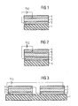
- FIG. 2 shows a component which has a layer structure comparable to that of FIG. 1 concerning the layers 2 to 4 and the substrate 1, but between the primary electrode 2 and the semiconducting layer 3 and between the semiconducting layer 3 and the secondary electrode 4 each an intermediate layer (5,6) is installed, through which the threshold voltage is displaceable.
- the intermediate layers 5, 6 may be made of a wide variety of materials, e.g. organic material such as polythiophene, polyfluorene (both materials doped or undoped), pani, pedot or oxidic material such as metal oxide or silicon oxide.
- FIG. 3 shows two components connected in series, the layer structure according to this embodiment being identical to that of the individual component of FIG.
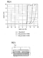
- Figure 4 shows the current-voltage characteristics of series connected devices. It can be seen how by the series connection of several components ( Figure 3) and a threshold voltage, which corresponds to the multiple of the threshold voltage of a single component, can be achieved.
- FIG. 5 shows the lateral structure of a component as is basically known from FIG. A substrate 1, a primary electrode 2, a semiconducting layer 3 and a secondary electrode 4 can again be seen.
- the threshold voltage can be set very well. Likewise, by one or two additional intermediate layers of other semiconductor materials such as thin insulating layers or oxides, the threshold voltage can be shifted.
- the series connection of several components also allows a rough adaptation to the respective requirements.
- the capacitance of the component is dependent on the layer thickness and the material-specific dielectric constant of the organic semiconductor. By means of correspondingly thick layers, the capacity can be kept small.
- the production of the device by means of known methods.
- the individual layers are formed by sputtering and / or evaporation or by soluble materials such as e.g. Polymers applied by spin coating and / or other coating methods and / or printing method.
- the structuring can be done on the one hand by conventional methods such as etching and lift-off in connection with lithography or on the other hand by printing techniques.
- the device e.g. 1, as follows: On a flexible polyester film 1, a metal layer 2 (for example gold) is sputtered, which is patterned by means of lithography and etching. Subsequently, a solubilized semiconducting polymer (e.g., polythiophene) is spin-coated. After evaporation of the solvent, a homogeneous semiconductive layer 3 is formed on top of which a secondary electrode 4 (e.g., aluminum) patterned by a shadow mask is sputtered onto.
- a metal layer 2 for example gold
- a solubilized semiconducting polymer e.g., polythiophene
- a homogeneous semiconductive layer 3 is formed on top of which a secondary electrode 4 (e.g., aluminum) patterned by a shadow mask is sputtered onto.
- organic includes all types of organic, organometallic and / or organic-inorganic plastics (hybrids), in particular those which are referred to in English as “plastics” , These are all types of materials, with the exception of semiconductors, which form the classical diodes (germanium, silicon), and the typical metallic conductor.
- a restriction in the dogmatic sense to organic material as carbon-containing Material is therefore not provided, but is also thought of the widespread use of eg silicones.
- the term should not be restricted in terms of molecular size, in particular to polymeric and / or oligomeric materials, but it is also quite possible to use "small molecules”.
- the word component "polymer” in the functional polymer is historically conditioned and thus contains no statement about the presence of an actual polymeric compound.
- an organic device is presented for the first time, which works as overvoltage protection and can be integrated into organic circuits.
Landscapes
- Engineering & Computer Science (AREA)
- Microelectronics & Electronic Packaging (AREA)
- Physics & Mathematics (AREA)
- Electromagnetism (AREA)
- Artificial Intelligence (AREA)
- Computer Vision & Pattern Recognition (AREA)
- General Physics & Mathematics (AREA)
- Theoretical Computer Science (AREA)
- Thin Film Transistor (AREA)
- Semiconductor Integrated Circuits (AREA)
- Emergency Protection Circuit Devices (AREA)
- Protection Of Static Devices (AREA)
Description
- Die Erfindung betrifft ein Bauelement aus vorwiegend organischem Material, das einen Überspannungsschutz für elektronische Schaltungen bietet.
- Es sind elektronische Bauelemente zum Überspannungsschutz basierend auf anorganischen, auf herkömmlicher Siliziumhalbleitertechnologie aufbauenden Schaltungen bekannt. Beispielhaft genannt seien Zener-Dioden und Tunnel-Dioden.
- Aus der Wo 96/02924 ist ein Element zum Überspannungsschutz bekannt, in dem organisches Material eingesetzt wird. Dort wird eine Dielektrikumsschicht aus polymerem Kunststoff oder Glas oder Keramik vorgeschlagen, die einerseits mit einer geerdeten Platte und andererseits mit einer leitfähigen Schicht in Kontakt ist. Die Dielektrikumsschicht kann verschiedene Füllstoffe enthalten, die ihr verschiedene Eigenschaften verleihen können. Es wird jedoch nicht im Hinblick auf low-cost products eine Verwendung halbleitender oder gar halbleitender organischer Materialien zum Überspannungsschutz vorgeschlagen.
- Organische elektronische Bauelemente und daraus aufgebaute Schaltungen werden im Hinblick auf lowest-cost Anwendungen wie RFID-Tags (Radio Frequency Identification), Tickets, Wearable electronics (elektronische Schaltungen, die in Textilien eingearbeitet sind), etc. entwickelt. Sie sind kostengünstig und durch einfache Druckprozesse großflächig herstellbar. Diese Schaltungen brauchen eine konstante Spannungsversorgung, wobei Schäden durch Spannungsspitzen, beispielsweise wenn die Schaltung der Sende-Antenne zu nahe kommt oder wenn man das RFID Tag zu schnell durch ein elektromagnetisches Wechselfeld bewegt, vermieden werden müssen. Es ist bislang noch kein elektronisches Bauelement bekannt, das - vergleichbar zum organischen Feld-Effekt-Transistor - vorwiegend organisches Material umfasst.
- Aufgabe der vorliegenden Erfindung ist es daher, ein elektronisches Bauelement zu schaffen, das vorwiegend organisches Material umfasst und das einen Überspannungsschutz bietet, das heißt bei Unter- oder Überschreiten einer einstellbaren Schwellwertspannung wirkt das Bauelement als Widerstand, der den Stromfluss unterbricht und umgekehrt, wobei die elektrische Kapazität des Bauteils gering ist.
- Gegenstand der Erfindung ist ein elektronisches Bauelement zum Überspannungschutz, zumindest eine organische halbleitende Funktionsschicht umfassend, zumindest folgende Schichten aufweisend:
- ein Substrat, darauf
- eine primäre Elektrode, dann
- eine organische halbleitende Funktionsschicht und darauf eine sekundäre Elektrode, wobei sich durch die Wahl der Elektrodenmaterialien und/oder des Materials für die halbleitende Schicht die Schwellwertspannung einstellen lässt. Außerdem ist Gegenstand der Erfindung eine Schaltung, zumindest zwei Bauelemente, die vorwiegend organische Materialien umfassen, zum Überspannungsschutz in Reihe geschaltet umfassend, wobei durch die Reihenschaltung eine Schwellwertspannung realisiert wird, die einem Mehrfachen der Schwellwertspannung der einzelnen Bauelemente entspricht.
- Nach einer Ausführungsform umfasst das Bauelement zumindest eine Zwischenschicht zwischen einer der Elektroden und der organischen Halbleiterschicht. Die Zwischenschicht kann beispielsweise vorwiegend aus organischem und/oder oxidischem Material sein. Durch das Einfügen der zumindest einen Zwischenschicht lässt sich die Schwellwertspannung innerhalb einiger Volt einstellen.
- Das Bauelement wird in Vorwärtsrichtung betrieben, das heißt, dass bis zu der Schwellwertspannung kein Strom (oder nur ein vernachlässigbar kleiner Strom) fließt, oberhalb der Schwellwertspannung hingegen ein sehr hoher Strom, so dass die Spannung einer leistungsbegrenzten Stromquelle zusammenbricht. In Sperrrichtung fließt kein Strom (oder nur ein vernachlässigbar kleiner Strom).
- Nach einer Ausführungsform werden zumindest zwei Bauelemente in Reihe geschaltet. Dadurch kann eine gewünschte Schwellwertspannung, welche dem Vielfachen der Schwellwertspannung der einzelnen Bauelemente entspricht, erreicht werden.
- Der einfache Aufbau des Bauelements aus leitenden und halbleitenden Schichten erlaubt eine Integration in organische Schaltungen. Die leitenden und/oder die halbleitenden Schichten können dabei durch ein Verfahren und/oder durch gemeinsame Prozessschritte, beispielsweise Druckverfahren, hergestellt werden.
- Im folgenden wird die Erfindung noch anhand von Ausführungsformen näher erläutert.
- Figur 1
- zeigt den einfachen Aufbau des erfindungsgemäßen Bauteils ohne Zwischenschichten.
- Figur 2
- zeigt ein Ausführungsbeispiel mit zwei Zwischenschichten,
- Figur 3
- zeigt zwei Bauelemente, die in Reihe geschaltet sind,
- Figur 4
- zeigt die entsprechenden Strom-Spannungskurven zu Figur 3 und
- Figur 5
- zeigt schließlich ein Bauelement mit einem lateralen Aufbau.
- In Figur 1 ist das Substrat 1, beispielsweise aus einer flexiblen Folie wie einer Polyester-Folie, zu sehen, darauf liegend (Realisierung des vertikalen Aufbaus) die primäre Elektrode 2, die beispielsweise aus organischem Material wie Pani, PEDOT oder aus Metallen oder Legierungen wie Gold, Kupfer, Aluminium, Titan ist, darauf befindlich die halbleitende Schicht 3, die auf organischer Basis aus beispielsweise Polythiophen und/oder Polyfluoren ist, darauf die sekundäre Elektrode 4, deren Material wieder beispielsweise Pani, Pedot oder ein Metall oder eine Legierung wie Gold, Kupfer, Aluminium, Titan ist. Im Gegensatz zu herkömmlichen Bauelementen hat dieses Bauelement eine hohe Schwellwertspannung, welche sich durch die Wahl der Elektrodenmaterialien und des Halbleitermaterials einstellen lässt.
- In Figur 2 ist ein Bauelement gezeigt, das einen mit der Figur 1 vergleichbaren Schichtaufbau betreffend die Schichten 2 bis 4 und das Substrat 1 hat, wobei jedoch zwischen der primären Elektrode 2 und der halbleitenden Schicht 3 sowie zwischen der halbleitenden Schicht 3 und der sekundären Elektrode 4 jeweils eine Zwischenschicht (5,6) eingebaut ist, durch die die Schwellwertspannung verschiebbar ist. Die Zwischenschichten 5,6 können aus verschiedensten Materialien sein, wie z.B. organischem Material wie Polythiophen, Polyfluoren (beide Materialien dotiert oder undotiert), Pani, Pedot oder aus oxidischem Material wie Metalloxid oder Siliziumoxid.
- Figur 3 zeigt zwei Bauelemente in Reihe geschaltet, wobei der Schichtaufbau nach dieser Ausführungsform dem des Einzelbauelements der Figur 1 gleicht.
- Figur 4 zeigt die Strom-Spannungskennlinien von in Reihe geschalteten Bauelementen. Dabei ist zu erkennen, wie durch die Reihenschaltung mehrerer Bauelemente (Figur 3) auch eine Schwellwertspannung, welche dem Vielfachen der Schwellwertspannung eines einzelnen Bauelements entspricht, erreicht werden kann.
- Schließlich zeigt Figur 5 den lateralen Aufbau eines Bauelements wie es grundsätzlich aus Figur 1 bekannt ist. Zu erkennen ist wieder ein Substrat 1, eine primäre Elektrode 2, eine halbleitende Schicht 3 und eine sekundäre Elektrode 4.
- Durch die Wahl geeigneter Elektroden und/oder Halbleitermaterialien lässt sich die Schwellwertspannung sehr gut einstellen. Ebenso kann durch ein oder zwei zusätzliche Zwischenschichten aus anderen Halbleitermaterialien wie z.B. dünnen Isolationsschichten oder Oxiden die Schwellwertspannung verschoben werden. Die Reihenschaltung mehrerer Bauelemente ermöglicht zudem eine grobe Anpassung an die jeweiligen Anforderungen.
- Die Kapazität des Bauelements ist abhängig von der Schichtdicke und der materialspezifischen Dielektrizitätszahl des organischen Halbleiters. Mittels entsprechend dicker Schichten kann die Kapazität klein gehalten werden.
- Die Herstellung des Bauelements erfolgt mittels bekannter Verfahren. Die einzelnen Schichten werden durch Sputtern und/oder Verdampfen oder aber bei löslichen Materialien wie z.B. Polymeren durch Spincoating und/oder anderen Beschichtungsverfahren und/oder Druckverfahren aufgebracht. Die Strukturierung kann einerseits durch herkömmliche Verfahren wie Ätzen und Lift-Off in Verbindung mit Lithographie vorgenommen werden oder andererseits durch Drucktechniken.
- Konkret kann das Bauelement, z.B. aus Figur 1, wie folgt hergestellt werden: Auf einer flexiblen Polyester Folie 1 wird eine Metallschicht 2 (z.B. Gold) aufgesputtert, welche mittels Lithographie und Ätzen strukturiert wird. Anschließend wird ein in Lösung gebrachtes halbleitendes Polymer (z.B. Polythiophen) durch Spincoating aufgeschleudert. Nach dem Verdampfen des Lösungsmittels entsteht eine homogene halbleitende Schicht 3. Auf diese wird eine sekundäre Elektrode 4 (z.B. Aluminium) - durch eine Schattenmaske strukturiert - aufgesputtert.
- Der Begriff "organisch", "organisches Material" oder "Funktionspolymer" oder "Polymer" umfasst hier alle Arten von organischen, metallorganischen und/oder organisch-anorganischen Kunststoffen (Hybride), insbesondere die, die im Englischen z.B. mit "plastics" bezeichnet werden. Es handelt sich um alle Arten von Stoffen mit Ausnahme der Halbleiter, die die klassischen Dioden bilden (Germanium, Silizium), und der typischen metallischen Leiter. Eine Beschränkung im dogmatischen Sinn auf organisches Material als Kohlenstoffenthaltendes Material ist demnach nicht vorgesehen, vielmehr ist auch an den breiten Einsatz von z.B. Siliconen gedacht. Weiterhin soll der Term keiner Beschränkung im Hinblick auf die Molekülgröße, insbesondere auf polymere und/oder oligomere Materialien unterliegen, sondern es ist durchaus auch der Einsatz von "small molecules" möglich. Der Wortbestandteil "polymer" im Funktionspolymer ist historisch bedingt und enthält insofern keine Aussage über das Vorliegen einer tatsächlich polymeren Verbindung.
- Mit dieser Erfindung wird erstmals ein organisches Bauelement vorgestellt, das als Überspannungsschutz funktioniert und in organische Schaltungen integriert werden kann.
Claims (3)
- Elektronisches Bauelement zum Überspannungsschutz, zumindest eine Schicht aus einem organischen halbleitenden Funktionspolymer und zwei leitfähige Schichten umfassend, wobei folgender Schichtaufbau realisiert ist:ein Substrat, daraufeine primäre Elektrode, daraufdie organische halbleitende Funktionsschicht und darauf eine sekundäre Elektrode, wobei sich durch die Wahl der Elektrodenmaterialien und/oder des Materials für die halbleitende Schicht die Schwellwertspannung einstellen lässt.
- Bauelement nach Anspruch 1, das zumindest eine Zwischenschicht zwischen einer der Elektroden und der organischen Halbleiterschicht hat.
- Schaltung, zumindest zwei Bauelemente nach einem der Ansprüche 1 oder 2, zum Überspannungsschutz in Reihe geschaltet umfassend, wobei durch die Reihenschaltung eine Schwellwertspannung realisiert wird, die einem Mehrfachen der Schwellwertspannung der einzelnen Bauelemente entspricht.
Applications Claiming Priority (3)
| Application Number | Priority Date | Filing Date | Title |
|---|---|---|---|
| DE10238800 | 2002-08-23 | ||
| DE10238800 | 2002-08-23 | ||
| PCT/DE2003/002612 WO2004021256A1 (de) | 2002-08-23 | 2003-08-04 | Organisches bauelement zum überspannungsschutz und dazugehörige schaltung |
Publications (2)
| Publication Number | Publication Date |
|---|---|
| EP1532570A1 EP1532570A1 (de) | 2005-05-25 |
| EP1532570B1 true EP1532570B1 (de) | 2007-02-28 |
Family
ID=31968990
Family Applications (1)
| Application Number | Title | Priority Date | Filing Date |
|---|---|---|---|
| EP03790673A Expired - Lifetime EP1532570B1 (de) | 2002-08-23 | 2003-08-04 | Organisches bauelement zum überspannungsschutz und dazugehörige schaltung |
Country Status (8)
| Country | Link |
|---|---|
| US (1) | US7414513B2 (de) |
| EP (1) | EP1532570B1 (de) |
| JP (1) | JP2005537637A (de) |
| CN (1) | CN100338791C (de) |
| AT (1) | ATE355566T1 (de) |
| DE (1) | DE50306683D1 (de) |
| ES (1) | ES2282722T3 (de) |
| WO (1) | WO2004021256A1 (de) |
Families Citing this family (5)
| Publication number | Priority date | Publication date | Assignee | Title |
|---|---|---|---|---|
| DE10043204A1 (de) * | 2000-09-01 | 2002-04-04 | Siemens Ag | Organischer Feld-Effekt-Transistor, Verfahren zur Strukturierung eines OFETs und integrierte Schaltung |
| US20080055086A1 (en) * | 2004-09-14 | 2008-03-06 | Koninklijke Philips Electronics, N.V. | Overvoltage Protection Device and Radio Frequency Receiver and Radio Frequency Identification Tag Comprising such a Device |
| DE102005031448A1 (de) | 2005-07-04 | 2007-01-11 | Polyic Gmbh & Co. Kg | Aktivierbare optische Schicht |
| KR20100037964A (ko) * | 2008-10-02 | 2010-04-12 | 삼성전자주식회사 | 트랜지스터, 그 제조 방법 및 트랜지스터의 문턱전압 조절방법 |
| DE102009013685B4 (de) * | 2009-03-20 | 2013-01-31 | Novaled Ag | Verwendung einer organischen Diode als organische Zenerdiode und Verfahren zum Betreiben |
Family Cites Families (169)
| Publication number | Priority date | Publication date | Assignee | Title |
|---|---|---|---|---|
| GB723598A (en) | 1951-09-07 | 1955-02-09 | Philips Nv | Improvements in or relating to methods of producing electrically conductive mouldings from plastics |
| US3512052A (en) | 1968-01-11 | 1970-05-12 | Gen Motors Corp | Metal-insulator-semiconductor voltage variable capacitor with controlled resistivity dielectric |
| US3769096A (en) | 1971-03-12 | 1973-10-30 | Bell Telephone Labor Inc | Pyroelectric devices |
| US3668483A (en) * | 1971-08-19 | 1972-06-06 | Us Navy | Direct current solid state circuit breaker |
| JPS543594B2 (de) | 1973-10-12 | 1979-02-24 | ||
| US3939363A (en) * | 1974-02-25 | 1976-02-17 | Westinghouse Electric Corporation | Circuitry with zener diode voltage surge suppressor connected to serve as half wave rectifier |
| JPS54101176A (en) | 1978-01-26 | 1979-08-09 | Shinetsu Polymer Co | Contact member for push switch |
| US4442019A (en) | 1978-05-26 | 1984-04-10 | Marks Alvin M | Electroordered dipole suspension |
| JPS5641938U (de) | 1979-09-10 | 1981-04-17 | ||
| US4340657A (en) | 1980-02-19 | 1982-07-20 | Polychrome Corporation | Novel radiation-sensitive articles |
| JPS5910554A (ja) | 1982-07-09 | 1984-01-20 | Dainippon Ink & Chem Inc | 新規ネマチツク液晶化合物 |
| JPS59145576A (ja) | 1982-11-09 | 1984-08-21 | ザイトレツクス・コ−ポレ−シヨン | プログラム可能なmosトランジスタ |
| JPS60117769A (ja) | 1983-11-30 | 1985-06-25 | Fujitsu Ltd | 半導体メモリ装置 |
| US4573099A (en) * | 1984-06-29 | 1986-02-25 | At&T Bell Laboratories | CMOS Circuit overvoltage protection |
| US4598331A (en) * | 1984-07-30 | 1986-07-01 | Technology Research Corporation | Ground fault current interrupter circuit with open neutral and ground lead protection |
| JPS61167854U (de) | 1985-04-10 | 1986-10-17 | ||
| DE3768112D1 (de) | 1986-03-03 | 1991-04-04 | Toshiba Kawasaki Kk | Strahlungsdetektor. |
| US4797773A (en) * | 1986-05-09 | 1989-01-10 | Transtector Systems, Inc. | Spatial array filtering system for electrical devices |
| DE3751376T2 (de) | 1986-10-13 | 1995-11-16 | Canon Kk | Schaltungselement. |
| JP2728412B2 (ja) | 1987-12-25 | 1998-03-18 | 株式会社日立製作所 | 半導体装置 |
| US5068634A (en) * | 1988-01-11 | 1991-11-26 | Electromer Corporation | Overvoltage protection device and material |
| US4977357A (en) * | 1988-01-11 | 1990-12-11 | Shrier Karen P | Overvoltage protection device and material |
| GB2215307B (en) | 1988-03-04 | 1991-10-09 | Unisys Corp | Electronic component transportation container |
| US4910389A (en) * | 1988-06-03 | 1990-03-20 | Raychem Corporation | Conductive polymer compositions |
| ATE100616T1 (de) | 1988-06-21 | 1994-02-15 | Gec Avery Ltd | Herstellung von tragbaren elektronischen karten. |
| US5364735A (en) | 1988-07-01 | 1994-11-15 | Sony Corporation | Multiple layer optical record medium with protective layers and method for producing same |
| US4937119A (en) | 1988-12-15 | 1990-06-26 | Hoechst Celanese Corp. | Textured organic optical data storage media and methods of preparation |
| US5892244A (en) | 1989-01-10 | 1999-04-06 | Mitsubishi Denki Kabushiki Kaisha | Field effect transistor including πconjugate polymer and liquid crystal display including the field effect transistor |
| US6331356B1 (en) | 1989-05-26 | 2001-12-18 | International Business Machines Corporation | Patterns of electrically conducting polymers and their application as electrodes or electrical contacts |
| DE69018348T2 (de) | 1989-07-25 | 1995-08-03 | Matsushita Electric Ind Co Ltd | Speicherbauelement aus organischem Halbleiter mit einer MISFET-Struktur und sein Kontrollverfahren. |
| US5206525A (en) | 1989-12-27 | 1993-04-27 | Nippon Petrochemicals Co., Ltd. | Electric element capable of controlling the electric conductivity of π-conjugated macromolecular materials |
| US5099380A (en) * | 1990-04-19 | 1992-03-24 | Electromer Corporation | Electrical connector with overvoltage protection feature |
| FR2664430B1 (fr) | 1990-07-04 | 1992-09-18 | Centre Nat Rech Scient | Transistor a effet de champ en couche mince de structure mis, dont l'isolant et le semiconducteur sont realises en materiaux organiques. |
| US5260848A (en) * | 1990-07-27 | 1993-11-09 | Electromer Corporation | Foldback switching material and devices |
| US5376561A (en) | 1990-12-31 | 1994-12-27 | Kopin Corporation | High density electronic circuit modules |
| US5142263A (en) * | 1991-02-13 | 1992-08-25 | Electromer Corporation | Surface mount device with overvoltage protection feature |
| FR2673041A1 (fr) | 1991-02-19 | 1992-08-21 | Gemplus Card Int | Procede de fabrication de micromodules de circuit integre et micromodule correspondant. |
| EP0501456A3 (de) | 1991-02-26 | 1992-09-09 | Sony Corporation | Mit eine optischen Plattenantrieb ausgerüsteter Videospielcomputer |
| US5408109A (en) | 1991-02-27 | 1995-04-18 | The Regents Of The University Of California | Visible light emitting diodes fabricated from soluble semiconducting polymers |
| JP3522771B2 (ja) | 1991-03-22 | 2004-04-26 | 三菱電機株式会社 | インバータ |
| US5332315A (en) | 1991-04-27 | 1994-07-26 | Gec Avery Limited | Apparatus and sensor unit for monitoring changes in a physical quantity with time |
| FR2676870B1 (fr) * | 1991-05-24 | 1994-12-23 | Sgs Thomson Microelectronics | Structure de protection dans un circuit cmos contre le verrouillage. |
| JPH0580530A (ja) | 1991-09-24 | 1993-04-02 | Hitachi Ltd | 薄膜パターン製造方法 |
| US5173835A (en) | 1991-10-15 | 1992-12-22 | Motorola, Inc. | Voltage variable capacitor |
| DE59105477D1 (de) | 1991-10-30 | 1995-06-14 | Fraunhofer Ges Forschung | Belichtungsvorrichtung. |
| JP2709223B2 (ja) | 1992-01-30 | 1998-02-04 | 三菱電機株式会社 | 非接触形携帯記憶装置 |
| JP3150750B2 (ja) | 1992-03-13 | 2001-03-26 | 日本写真印刷株式会社 | 有機整流素子 |
| JPH05347422A (ja) | 1992-06-16 | 1993-12-27 | Fujitsu Ltd | 二安定ダイオード |
| JP3457348B2 (ja) | 1993-01-15 | 2003-10-14 | 株式会社東芝 | 半導体装置の製造方法 |
| WO1994017556A1 (en) | 1993-01-26 | 1994-08-04 | Fci-Fiberchem, Inc. | Optical sensor with electroluminescent light source and polymer light detector |
| FR2701117B1 (fr) | 1993-02-04 | 1995-03-10 | Asulab Sa | Système de mesures électrochimiques à capteur multizones, et son application au dosage du glucose. |
| US5567550A (en) | 1993-03-25 | 1996-10-22 | Texas Instruments Incorporated | Method of making a mask for making integrated circuits |
| JPH0722669A (ja) | 1993-07-01 | 1995-01-24 | Mitsubishi Electric Corp | 可塑性機能素子 |
| JP3035352B2 (ja) | 1993-08-24 | 2000-04-24 | メトリカ・インコーポレーテッド | 新規な使い捨て電子検定ディバイス |
| JP3460863B2 (ja) | 1993-09-17 | 2003-10-27 | 三菱電機株式会社 | 半導体装置の製造方法 |
| FR2710413B1 (fr) | 1993-09-21 | 1995-11-03 | Asulab Sa | Dispositif de mesure pour capteurs amovibles. |
| US5556706A (en) | 1993-10-06 | 1996-09-17 | Matsushita Electric Industrial Co., Ltd. | Conductive layered product and method of manufacturing the same |
| DE69531477T2 (de) | 1994-05-16 | 2004-07-15 | Koninklijke Philips Electronics N.V. | Halbleiteranordnung aus halbleitendem, organischem material |
| WO1995031831A1 (en) | 1994-05-18 | 1995-11-23 | Philips Electronics N.V. | Method of providing a film of conjugated, substituted or unsubstituted poly(p-phenylene vinylene) on a substrate by chemical vapour deposition (cvd), as well as a method of manufacturing an electroluminescent (el) device |
| US5684884A (en) | 1994-05-31 | 1997-11-04 | Hitachi Metals, Ltd. | Piezoelectric loudspeaker and a method for manufacturing the same |
| JP3246189B2 (ja) | 1994-06-28 | 2002-01-15 | 株式会社日立製作所 | 半導体表示装置 |
| ATE227881T1 (de) | 1994-07-14 | 2002-11-15 | Surgx Corp | Verfahren zur herstellung von ein- und mehrschicht-schutzvorrichtungen gegen veränderliche spannung |
| DE4426307C2 (de) * | 1994-07-25 | 2003-05-28 | Bosch Gmbh Robert | Integrierte Schaltung mit einem Gate Oxid und Testmöglichkeit für dieses bei der Herstellung |
| EP0709944A1 (de) * | 1994-10-31 | 1996-05-01 | STMicroelectronics S.r.l. | Spannungsregler für ein Batterieladesystem |
| US5574291A (en) | 1994-12-09 | 1996-11-12 | Lucent Technologies Inc. | Article comprising a thin film transistor with low conductivity organic layer |
| US5630986A (en) | 1995-01-13 | 1997-05-20 | Bayer Corporation | Dispensing instrument for fluid monitoring sensors |
| JPH08197788A (ja) | 1995-01-27 | 1996-08-06 | Hitachi Koki Co Ltd | プリンタ制御装置の画像データ読出し回路 |
| JP3068430B2 (ja) | 1995-04-25 | 2000-07-24 | 富山日本電気株式会社 | 固体電解コンデンサ及びその製造方法 |
| US5652645A (en) | 1995-07-24 | 1997-07-29 | Anvik Corporation | High-throughput, high-resolution, projection patterning system for large, flexible, roll-fed, electronic-module substrates |
| GB9519698D0 (en) | 1995-09-27 | 1995-11-29 | Rivaz Antony C De | Educational toys and games |
| WO1997018944A1 (en) | 1995-11-22 | 1997-05-29 | The Government Of The United States Of America, Represented By The Secretary Of The Navy | Patterned conducting polymer surfaces and process for preparing the same and devices containing the same |
| US5625199A (en) | 1996-01-16 | 1997-04-29 | Lucent Technologies Inc. | Article comprising complementary circuit with inorganic n-channel and organic p-channel thin film transistors |
| US6326640B1 (en) | 1996-01-29 | 2001-12-04 | Motorola, Inc. | Organic thin film transistor with enhanced carrier mobility |
| GB2310493B (en) | 1996-02-26 | 2000-08-02 | Unilever Plc | Determination of the characteristics of fluid |
| DE19629656A1 (de) | 1996-07-23 | 1998-01-29 | Boehringer Mannheim Gmbh | Diagnostischer Testträger mit mehrschichtigem Testfeld und Verfahren zur Bestimmung von Analyt mit dessen Hilfe |
| JP3724589B2 (ja) * | 1996-07-29 | 2005-12-07 | ケンブリッジ ディスプレイ テクノロジー リミテッド | エレクトロルミネセンス素子 |
| AUPO307296A0 (en) * | 1996-10-18 | 1996-11-14 | Erico Lightning Technologies Pty Ltd | An improved lightning conductor |
| WO1998040930A1 (en) | 1997-03-10 | 1998-09-17 | Precision Dynamics Corporation | Reactively coupled elements in circuits on flexible substrates |
| US5946551A (en) | 1997-03-25 | 1999-08-31 | Dimitrakopoulos; Christos Dimitrios | Fabrication of thin film effect transistor comprising an organic semiconductor and chemical solution deposited metal oxide gate dielectric |
| US6344662B1 (en) * | 1997-03-25 | 2002-02-05 | International Business Machines Corporation | Thin-film field-effect transistor with organic-inorganic hybrid semiconductor requiring low operating voltages |
| KR100248392B1 (ko) | 1997-05-15 | 2000-09-01 | 정선종 | 유기물전계효과트랜지스터와결합된유기물능동구동전기발광소자및그소자의제작방법 |
| GB9715907D0 (en) | 1997-07-29 | 1997-10-01 | Cambridge Consultants | Electroluminescent device production process |
| EP0968537B1 (de) | 1997-08-22 | 2012-05-02 | Creator Technology B.V. | Feld-effekt-transistor, der im wesentlichen aus organischen materialien besteht |
| WO1999010929A2 (en) | 1997-08-22 | 1999-03-04 | Koninklijke Philips Electronics N.V. | A method of providing a vertical interconnect between thin film microelectronic devices |
| AU764920B2 (en) | 1997-09-11 | 2003-09-04 | Precision Dynamics Corporation | Radio frequency identification tag on flexible substrate |
| WO1999021233A1 (en) | 1997-10-17 | 1999-04-29 | The Regents Of The University Of California | Process for fabricating organic semiconductor devices using ink-jet printing technology and device and system employing same |
| US6251513B1 (en) | 1997-11-08 | 2001-06-26 | Littlefuse, Inc. | Polymer composites for overvoltage protection |
| US5997817A (en) | 1997-12-05 | 1999-12-07 | Roche Diagnostics Corporation | Electrochemical biosensor test strip |
| JP2001510670A (ja) | 1997-12-05 | 2001-07-31 | コーニンクレッカ フィリップス エレクトロニクス エヌ ヴィ | 識別トランスポンダ |
| US5998805A (en) | 1997-12-11 | 1999-12-07 | Motorola, Inc. | Active matrix OED array with improved OED cathode |
| NO306529B1 (no) | 1998-01-16 | 1999-11-15 | Opticom As | Transistor |
| US6083104A (en) | 1998-01-16 | 2000-07-04 | Silverlit Toys (U.S.A.), Inc. | Programmable toy with an independent game cartridge |
| JP3911566B2 (ja) * | 1998-01-27 | 2007-05-09 | 富士電機デバイステクノロジー株式会社 | Mos型半導体装置 |
| AU739848B2 (en) | 1998-01-28 | 2001-10-18 | Thin Film Electronics Asa | A method for generation of electrical conducting or semiconducting structures in three dimensions and methods for erasure of the same structures |
| US6087196A (en) | 1998-01-30 | 2000-07-11 | The Trustees Of Princeton University | Fabrication of organic semiconductor devices using ink jet printing |
| US6045977A (en) | 1998-02-19 | 2000-04-04 | Lucent Technologies Inc. | Process for patterning conductive polyaniline films |
| US6033202A (en) | 1998-03-27 | 2000-03-07 | Lucent Technologies Inc. | Mold for non - photolithographic fabrication of microstructures |
| GB9808061D0 (en) | 1998-04-16 | 1998-06-17 | Cambridge Display Tech Ltd | Polymer devices |
| TW410478B (en) | 1998-05-29 | 2000-11-01 | Lucent Technologies Inc | Thin-film transistor monolithically integrated with an organic light-emitting diode |
| US5967048A (en) | 1998-06-12 | 1999-10-19 | Howard A. Fromson | Method and apparatus for the multiple imaging of a continuous web |
| KR100282393B1 (ko) | 1998-06-17 | 2001-02-15 | 구자홍 | 유기이엘(el)디스플레이소자제조방법 |
| US6528816B1 (en) | 1998-06-19 | 2003-03-04 | Thomas Jackson | Integrated inorganic/organic complementary thin-film transistor circuit and a method for its production |
| US6215130B1 (en) | 1998-08-20 | 2001-04-10 | Lucent Technologies Inc. | Thin film transistors |
| JP4689825B2 (ja) | 1998-08-26 | 2011-05-25 | センサーズ・フォー・メデセン・アンド・サイエンス・インコーポレーテッド | 光学式検知装置 |
| JP4493741B2 (ja) | 1998-09-04 | 2010-06-30 | 株式会社半導体エネルギー研究所 | 半導体装置の作製方法 |
| US6384804B1 (en) | 1998-11-25 | 2002-05-07 | Lucent Techonologies Inc. | Display comprising organic smart pixels |
| GB9825992D0 (en) | 1998-11-28 | 1999-01-20 | Moorlodge Biotech Ventures Lim | Electrochemical sensor |
| US6506438B2 (en) | 1998-12-15 | 2003-01-14 | E Ink Corporation | Method for printing of transistor arrays on plastic substrates |
| US6321571B1 (en) | 1998-12-21 | 2001-11-27 | Corning Incorporated | Method of making glass structures for flat panel displays |
| US6114088A (en) | 1999-01-15 | 2000-09-05 | 3M Innovative Properties Company | Thermal transfer element for forming multilayer devices |
| GB2347013A (en) | 1999-02-16 | 2000-08-23 | Sharp Kk | Charge-transport structures |
| US6300141B1 (en) | 1999-03-02 | 2001-10-09 | Helix Biopharma Corporation | Card-based biosensor device |
| US6207472B1 (en) | 1999-03-09 | 2001-03-27 | International Business Machines Corporation | Low temperature thin film transistor fabrication |
| US6498114B1 (en) | 1999-04-09 | 2002-12-24 | E Ink Corporation | Method for forming a patterned semiconductor film |
| US6072716A (en) | 1999-04-14 | 2000-06-06 | Massachusetts Institute Of Technology | Memory structures and methods of making same |
| US6383664B2 (en) | 1999-05-11 | 2002-05-07 | The Dow Chemical Company | Electroluminescent or photocell device having protective packaging |
| CN1139137C (zh) * | 1999-06-16 | 2004-02-18 | 复旦大学 | 一种有机电双稳器件 |
| CA2374236C (en) | 1999-06-21 | 2014-12-23 | Cambridge University Technical Services Limited | Aligned polymers for an organic tft |
| TW556357B (en) | 1999-06-28 | 2003-10-01 | Semiconductor Energy Lab | Method of manufacturing an electro-optical device |
| CA2377671C (en) | 1999-07-01 | 2011-01-04 | David F. Bocian | High density non-volatile memory device |
| JP2001085272A (ja) | 1999-07-14 | 2001-03-30 | Matsushita Electric Ind Co Ltd | 可変容量コンデンサ |
| AU6174700A (en) | 1999-07-20 | 2001-02-05 | Alvin Wai Lun Yip | Carrier tray for integrated circuits such as microprocessors |
| ATE549753T1 (de) | 1999-07-21 | 2012-03-15 | E Ink Corp | Reaktive herstellung von dielektrischen schichten und schutz von organischen schichten in organischen halbleiteranordnungen |
| CN1183595C (zh) | 1999-08-24 | 2005-01-05 | 皇家菲利浦电子有限公司 | 显示装置 |
| JP4972260B2 (ja) | 1999-08-31 | 2012-07-11 | イー インク コーポレイション | パターニングされた半導体膜を形成する方法 |
| US6545291B1 (en) | 1999-08-31 | 2003-04-08 | E Ink Corporation | Transistor design for use in the construction of an electronically driven display |
| US6593690B1 (en) | 1999-09-03 | 2003-07-15 | 3M Innovative Properties Company | Large area organic electronic devices having conducting polymer buffer layers and methods of making same |
| US6517995B1 (en) | 1999-09-14 | 2003-02-11 | Massachusetts Institute Of Technology | Fabrication of finely featured devices by liquid embossing |
| US6340822B1 (en) | 1999-10-05 | 2002-01-22 | Agere Systems Guardian Corp. | Article comprising vertically nano-interconnected circuit devices and method for making the same |
| JP2004538618A (ja) | 1999-10-11 | 2004-12-24 | コーニンクレッカ フィリップス エレクトロニクス エヌ ヴィ | 集積回路 |
| US6335539B1 (en) | 1999-11-05 | 2002-01-01 | International Business Machines Corporation | Method for improving performance of organic semiconductors in bottom electrode structure |
| US6284562B1 (en) | 1999-11-17 | 2001-09-04 | Agere Systems Guardian Corp. | Thin film transistors |
| US6621098B1 (en) | 1999-11-29 | 2003-09-16 | The Penn State Research Foundation | Thin-film transistor and methods of manufacturing and incorporating a semiconducting organic material |
| US6136702A (en) | 1999-11-29 | 2000-10-24 | Lucent Technologies Inc. | Thin film transistors |
| US6197663B1 (en) | 1999-12-07 | 2001-03-06 | Lucent Technologies Inc. | Process for fabricating integrated circuit devices having thin film transistors |
| AU2015901A (en) | 1999-12-21 | 2001-07-03 | Plastic Logic Limited | Inkjet-fabricated integrated circuits |
| CN1245769C (zh) | 1999-12-21 | 2006-03-15 | 造型逻辑有限公司 | 溶液加工 |
| AU779878B2 (en) | 1999-12-21 | 2005-02-17 | Flexenable Limited | Forming interconnects |
| US6706159B2 (en) | 2000-03-02 | 2004-03-16 | Diabetes Diagnostics | Combined lancet and electrochemical analyte-testing apparatus |
| HK1053151B (en) | 2000-03-28 | 2006-05-26 | Diabetes Diagnostics, Inc. | Continuous process for manufacture of disposable electro-chemical sensor |
| US6329226B1 (en) | 2000-06-01 | 2001-12-11 | Agere Systems Guardian Corp. | Method for fabricating a thin-film transistor |
| DE10033112C2 (de) | 2000-07-07 | 2002-11-14 | Siemens Ag | Verfahren zur Herstellung und Strukturierung organischer Feldeffekt-Transistoren (OFET), hiernach gefertigter OFET und seine Verwendung |
| US6867539B1 (en) | 2000-07-12 | 2005-03-15 | 3M Innovative Properties Company | Encapsulated organic electronic devices and method for making same |
| WO2002015264A2 (de) | 2000-08-18 | 2002-02-21 | Siemens Aktiengesellschaft | Verkapseltes organisch-elektronisches bauteil, verfahren zu seiner herstellung und seine verwendung |
| DE10043204A1 (de) | 2000-09-01 | 2002-04-04 | Siemens Ag | Organischer Feld-Effekt-Transistor, Verfahren zur Strukturierung eines OFETs und integrierte Schaltung |
| DE10045192A1 (de) | 2000-09-13 | 2002-04-04 | Siemens Ag | Organischer Datenspeicher, RFID-Tag mit organischem Datenspeicher, Verwendung eines organischen Datenspeichers |
| GB0024294D0 (en) | 2000-10-04 | 2000-11-15 | Univ Cambridge Tech | Solid state embossing of polymer devices |
| KR20020036916A (ko) | 2000-11-11 | 2002-05-17 | 주승기 | 실리콘 박막의 결정화 방법 및 이에 의해 제조된 반도체소자 |
| NO20005980L (no) | 2000-11-27 | 2002-05-28 | Thin Film Electronics Ab | Ferroelektrisk minnekrets og fremgangsmåte ved dens fremstilling |
| KR100390522B1 (ko) | 2000-12-01 | 2003-07-07 | 피티플러스(주) | 결정질 실리콘 활성층을 포함하는 박막트랜지스터 제조 방법 |
| DE10061297C2 (de) | 2000-12-08 | 2003-05-28 | Siemens Ag | Verfahren zur Sturkturierung eines OFETs |
| DE10105914C1 (de) | 2001-02-09 | 2002-10-10 | Siemens Ag | Organischer Feldeffekt-Transistor mit fotostrukturiertem Gate-Dielektrikum und ein Verfahren zu dessen Erzeugung |
| EP1237207B1 (de) | 2001-03-02 | 2012-01-04 | FUJIFILM Corporation | Herstellungsverfahren einer organischen Dünnschicht-Vorrichtung |
| SE520339C2 (sv) | 2001-03-07 | 2003-06-24 | Acreo Ab | Elektrokemisk transistoranordning och dess tillverkningsförfarande |
| WO2002071139A1 (en) | 2001-03-07 | 2002-09-12 | Acreo Ab | Electrochemical pixel device |
| AU2002340793A1 (en) | 2001-05-07 | 2002-11-18 | Coatue Corporation | Molecular memory device |
| US20020170897A1 (en) | 2001-05-21 | 2002-11-21 | Hall Frank L. | Methods for preparing ball grid array substrates via use of a laser |
| EP1393389B1 (de) | 2001-05-23 | 2018-12-05 | Flexenable Limited | Musterung von anordnungen mittels laser |
| DE10126860C2 (de) | 2001-06-01 | 2003-05-28 | Siemens Ag | Organischer Feldeffekt-Transistor, Verfahren zu seiner Herstellung und Verwendung zum Aufbau integrierter Schaltungen |
| US6870180B2 (en) | 2001-06-08 | 2005-03-22 | Lucent Technologies Inc. | Organic polarizable gate transistor apparatus and method |
| JP2003089259A (ja) | 2001-09-18 | 2003-03-25 | Hitachi Ltd | パターン形成方法およびパターン形成装置 |
| US7351660B2 (en) | 2001-09-28 | 2008-04-01 | Hrl Laboratories, Llc | Process for producing high performance interconnects |
| CN1173978C (zh) * | 2001-10-11 | 2004-11-03 | 复旦大学 | 一种具有硫杂螺环结构的有机分子电子材料及其制备方法 |
| JP2003234473A (ja) | 2002-02-06 | 2003-08-22 | Canon Inc | 有機半導体素子の製造方法 |
| FI20020296A7 (fi) | 2002-02-14 | 2003-08-15 | Rafsec Oy | Älytarra |
| US6946332B2 (en) | 2002-03-15 | 2005-09-20 | Lucent Technologies Inc. | Forming nanoscale patterned thin film metal layers |
| US6812509B2 (en) | 2002-06-28 | 2004-11-02 | Palo Alto Research Center Inc. | Organic ferroelectric memory cells |
| US6870183B2 (en) | 2002-11-04 | 2005-03-22 | Advanced Micro Devices, Inc. | Stacked organic memory devices and methods of operating and fabricating |
| EP1559148A2 (de) | 2002-11-05 | 2005-08-03 | Siemens Aktiengesellschaft | ORGANISCHES ELEKTRONISCHES BAUTEIL MIT HOCHAUFGELöSTER STRUKTURIERUNG UND HERSTELLUNGSVERFAHREN DAZU |
-
2003
- 2003-08-04 CN CNB038200430A patent/CN100338791C/zh not_active Expired - Fee Related
- 2003-08-04 DE DE50306683T patent/DE50306683D1/de not_active Expired - Lifetime
- 2003-08-04 US US10/524,646 patent/US7414513B2/en not_active Expired - Fee Related
- 2003-08-04 ES ES03790673T patent/ES2282722T3/es not_active Expired - Lifetime
- 2003-08-04 AT AT03790673T patent/ATE355566T1/de active
- 2003-08-04 JP JP2004531439A patent/JP2005537637A/ja active Pending
- 2003-08-04 WO PCT/DE2003/002612 patent/WO2004021256A1/de not_active Ceased
- 2003-08-04 EP EP03790673A patent/EP1532570B1/de not_active Expired - Lifetime
Also Published As
| Publication number | Publication date |
|---|---|
| CN1679043A (zh) | 2005-10-05 |
| US20060098362A1 (en) | 2006-05-11 |
| ATE355566T1 (de) | 2006-03-15 |
| DE50306683D1 (de) | 2007-04-12 |
| HK1075524A1 (en) | 2005-12-16 |
| JP2005537637A (ja) | 2005-12-08 |
| ES2282722T3 (es) | 2007-10-16 |
| EP1532570A1 (de) | 2005-05-25 |
| WO2004021256A1 (de) | 2004-03-11 |
| CN100338791C (zh) | 2007-09-19 |
| US7414513B2 (en) | 2008-08-19 |
Similar Documents
| Publication | Publication Date | Title |
|---|---|---|
| WO2002015293A2 (de) | Organischer feldeffekt-transistor (ofet), herstellungsverfahren dazu und daraus gebaute integrierte schaltung sowie verwendungen | |
| EP1636826B1 (de) | Verbindung zur bildung einer selbstorganisierenden monolage, schichtstruktur, halbleiterbauelement mit einer schichtstruktur und verfahren zur herstellung einer schichtstruktur | |
| WO2002021612A1 (de) | Organischer gleichrichter, schaltung, rfid-tag und verwendung eines organischen gleichrichters | |
| DE10045192A1 (de) | Organischer Datenspeicher, RFID-Tag mit organischem Datenspeicher, Verwendung eines organischen Datenspeichers | |
| DE602004005824T2 (de) | Elektronische vorrichtung | |
| EP1825516A2 (de) | Gatter aus organischen feldeffekttransistoren | |
| WO2005020257A2 (de) | Organischer kondensator mit spannungsgesteuerter kapazität | |
| DE10209400A1 (de) | Transponderschaltung mit einer Gleichrichterschaltung sowie Verfahren zur Herstellung einer Transponderschaltung mit einer Gleichrichterschaltung | |
| EP1928037A2 (de) | Verfahren zur Herstellung eines organischen Dünnfilmtransistors durch Oxidation und selektive Reduktion von organischem Halbleitermaterial | |
| EP1436850A1 (de) | Isolator für ein organisches elektronikbauteil | |
| WO2004021256A1 (de) | Organisches bauelement zum überspannungsschutz und dazugehörige schaltung | |
| DE102008026216A1 (de) | Elektronische Schaltung | |
| WO2004093002A1 (de) | Transponder und verfahren zu dessen herstellung | |
| DE10226370B4 (de) | Substrat für ein elektronisches Bauteil, Verwendung des Substrates, Verfahren zur Erhöhung der Ladungsträgermobilität und Organischer Feld-Effekt Transistor (OFET) | |
| WO2006108514A2 (de) | Mehrschichtiger verbundkörper mit elektronischer funktion | |
| EP1704606B1 (de) | Verfahren zur Herstellung eines organischen Transistors mit selbstjustierender Gate-Elektrode | |
| DE19843956C1 (de) | Randstruktur für eine Halbleitervorrichtung | |
| DE102008036736B4 (de) | Elektrisches Installationsschaltgerät mit einer elektronischen Baugruppe | |
| DE10057502A1 (de) | Organischer Feld-Effekt-Transistor | |
| HK1075524B (en) | Organic component for overvoltage protection and associated circuit | |
| DE202005017580U1 (de) | Nano-elektronische Bauelemente |
Legal Events
| Date | Code | Title | Description |
|---|---|---|---|
| PUAI | Public reference made under article 153(3) epc to a published international application that has entered the european phase |
Free format text: ORIGINAL CODE: 0009012 |
|
| 17P | Request for examination filed |
Effective date: 20050212 |
|
| AK | Designated contracting states |
Kind code of ref document: A1 Designated state(s): AT BE BG CH CY CZ DE DK EE ES FI FR GB GR HU IE IT LI LU MC NL PT RO SE SI SK TR |
|
| RAP1 | Party data changed (applicant data changed or rights of an application transferred) |
Owner name: POLYIC GMBH & CO. KG |
|
| REG | Reference to a national code |
Ref country code: HK Ref legal event code: DE Ref document number: 1075524 Country of ref document: HK |
|
| GRAP | Despatch of communication of intention to grant a patent |
Free format text: ORIGINAL CODE: EPIDOSNIGR1 |
|
| GRAS | Grant fee paid |
Free format text: ORIGINAL CODE: EPIDOSNIGR3 |
|
| GRAA | (expected) grant |
Free format text: ORIGINAL CODE: 0009210 |
|
| RAP1 | Party data changed (applicant data changed or rights of an application transferred) |
Owner name: POLYIC GMBH & CO. KG |
|
| AK | Designated contracting states |
Kind code of ref document: B1 Designated state(s): AT BE BG CH CY CZ DE DK EE ES FI FR GB GR HU IE IT LI LU MC NL PT RO SE SI SK TR |
|
| PG25 | Lapsed in a contracting state [announced via postgrant information from national office to epo] |
Ref country code: FI Free format text: LAPSE BECAUSE OF FAILURE TO SUBMIT A TRANSLATION OF THE DESCRIPTION OR TO PAY THE FEE WITHIN THE PRESCRIBED TIME-LIMIT Effective date: 20070228 Ref country code: DK Free format text: LAPSE BECAUSE OF FAILURE TO SUBMIT A TRANSLATION OF THE DESCRIPTION OR TO PAY THE FEE WITHIN THE PRESCRIBED TIME-LIMIT Effective date: 20070228 Ref country code: SI Free format text: LAPSE BECAUSE OF FAILURE TO SUBMIT A TRANSLATION OF THE DESCRIPTION OR TO PAY THE FEE WITHIN THE PRESCRIBED TIME-LIMIT Effective date: 20070228 |
|
| REG | Reference to a national code |
Ref country code: GB Ref legal event code: FG4D Free format text: NOT ENGLISH |
|
| REG | Reference to a national code |
Ref country code: CH Ref legal event code: EP |
|
| REF | Corresponds to: |
Ref document number: 50306683 Country of ref document: DE Date of ref document: 20070412 Kind code of ref document: P |
|
| REG | Reference to a national code |
Ref country code: IE Ref legal event code: FG4D Free format text: LANGUAGE OF EP DOCUMENT: GERMAN |
|
| PG25 | Lapsed in a contracting state [announced via postgrant information from national office to epo] |
Ref country code: BG Free format text: LAPSE BECAUSE OF EXPIRATION OF PROTECTION Effective date: 20070529 |
|
| PG25 | Lapsed in a contracting state [announced via postgrant information from national office to epo] |
Ref country code: SE Free format text: LAPSE BECAUSE OF FAILURE TO SUBMIT A TRANSLATION OF THE DESCRIPTION OR TO PAY THE FEE WITHIN THE PRESCRIBED TIME-LIMIT Effective date: 20070531 |
|
| REG | Reference to a national code |
Ref country code: CH Ref legal event code: NV Representative=s name: FIAMMENGHI-FIAMMENGHI |
|
| REG | Reference to a national code |
Ref country code: HK Ref legal event code: GR Ref document number: 1075524 Country of ref document: HK |
|
| GBT | Gb: translation of ep patent filed (gb section 77(6)(a)/1977) |
Effective date: 20070627 |
|
| PG25 | Lapsed in a contracting state [announced via postgrant information from national office to epo] |
Ref country code: PT Free format text: LAPSE BECAUSE OF FAILURE TO SUBMIT A TRANSLATION OF THE DESCRIPTION OR TO PAY THE FEE WITHIN THE PRESCRIBED TIME-LIMIT Effective date: 20070730 |
|
| ET | Fr: translation filed | ||
| REG | Reference to a national code |
Ref country code: ES Ref legal event code: FG2A Ref document number: 2282722 Country of ref document: ES Kind code of ref document: T3 |
|
| PG25 | Lapsed in a contracting state [announced via postgrant information from national office to epo] |
Ref country code: SK Free format text: LAPSE BECAUSE OF FAILURE TO SUBMIT A TRANSLATION OF THE DESCRIPTION OR TO PAY THE FEE WITHIN THE PRESCRIBED TIME-LIMIT Effective date: 20070228 |
|
| REG | Reference to a national code |
Ref country code: IE Ref legal event code: FD4D |
|
| PG25 | Lapsed in a contracting state [announced via postgrant information from national office to epo] |
Ref country code: RO Free format text: LAPSE BECAUSE OF FAILURE TO SUBMIT A TRANSLATION OF THE DESCRIPTION OR TO PAY THE FEE WITHIN THE PRESCRIBED TIME-LIMIT Effective date: 20070228 Ref country code: CZ Free format text: LAPSE BECAUSE OF FAILURE TO SUBMIT A TRANSLATION OF THE DESCRIPTION OR TO PAY THE FEE WITHIN THE PRESCRIBED TIME-LIMIT Effective date: 20070228 |
|
| PLBE | No opposition filed within time limit |
Free format text: ORIGINAL CODE: 0009261 |
|
| STAA | Information on the status of an ep patent application or granted ep patent |
Free format text: STATUS: NO OPPOSITION FILED WITHIN TIME LIMIT |
|
| PG25 | Lapsed in a contracting state [announced via postgrant information from national office to epo] |
Ref country code: IE Free format text: LAPSE BECAUSE OF FAILURE TO SUBMIT A TRANSLATION OF THE DESCRIPTION OR TO PAY THE FEE WITHIN THE PRESCRIBED TIME-LIMIT Effective date: 20070228 |
|
| 26N | No opposition filed |
Effective date: 20071129 |
|
| BERE | Be: lapsed |
Owner name: POLYIC G.M.B.H. & CO. KG Effective date: 20070831 |
|
| PG25 | Lapsed in a contracting state [announced via postgrant information from national office to epo] |
Ref country code: GR Free format text: LAPSE BECAUSE OF FAILURE TO SUBMIT A TRANSLATION OF THE DESCRIPTION OR TO PAY THE FEE WITHIN THE PRESCRIBED TIME-LIMIT Effective date: 20070529 Ref country code: MC Free format text: LAPSE BECAUSE OF NON-PAYMENT OF DUE FEES Effective date: 20070831 |
|
| PG25 | Lapsed in a contracting state [announced via postgrant information from national office to epo] |
Ref country code: BE Free format text: LAPSE BECAUSE OF NON-PAYMENT OF DUE FEES Effective date: 20070831 |
|
| PG25 | Lapsed in a contracting state [announced via postgrant information from national office to epo] |
Ref country code: EE Free format text: LAPSE BECAUSE OF FAILURE TO SUBMIT A TRANSLATION OF THE DESCRIPTION OR TO PAY THE FEE WITHIN THE PRESCRIBED TIME-LIMIT Effective date: 20070228 |
|
| PG25 | Lapsed in a contracting state [announced via postgrant information from national office to epo] |
Ref country code: CY Free format text: LAPSE BECAUSE OF FAILURE TO SUBMIT A TRANSLATION OF THE DESCRIPTION OR TO PAY THE FEE WITHIN THE PRESCRIBED TIME-LIMIT Effective date: 20070228 |
|
| PG25 | Lapsed in a contracting state [announced via postgrant information from national office to epo] |
Ref country code: LU Free format text: LAPSE BECAUSE OF NON-PAYMENT OF DUE FEES Effective date: 20070804 |
|
| PG25 | Lapsed in a contracting state [announced via postgrant information from national office to epo] |
Ref country code: HU Free format text: LAPSE BECAUSE OF FAILURE TO SUBMIT A TRANSLATION OF THE DESCRIPTION OR TO PAY THE FEE WITHIN THE PRESCRIBED TIME-LIMIT Effective date: 20070901 Ref country code: TR Free format text: LAPSE BECAUSE OF FAILURE TO SUBMIT A TRANSLATION OF THE DESCRIPTION OR TO PAY THE FEE WITHIN THE PRESCRIBED TIME-LIMIT Effective date: 20070228 |
|
| PGFP | Annual fee paid to national office [announced via postgrant information from national office to epo] |
Ref country code: CH Payment date: 20110824 Year of fee payment: 9 |
|
| PGFP | Annual fee paid to national office [announced via postgrant information from national office to epo] |
Ref country code: ES Payment date: 20120824 Year of fee payment: 10 Ref country code: IT Payment date: 20120824 Year of fee payment: 10 |
|
| PGFP | Annual fee paid to national office [announced via postgrant information from national office to epo] |
Ref country code: AT Payment date: 20120822 Year of fee payment: 10 |
|
| PGFP | Annual fee paid to national office [announced via postgrant information from national office to epo] |
Ref country code: NL Payment date: 20130822 Year of fee payment: 11 Ref country code: DE Payment date: 20130803 Year of fee payment: 11 |
|
| PGFP | Annual fee paid to national office [announced via postgrant information from national office to epo] |
Ref country code: FR Payment date: 20130820 Year of fee payment: 11 Ref country code: GB Payment date: 20130823 Year of fee payment: 11 |
|
| REG | Reference to a national code |
Ref country code: CH Ref legal event code: PL |
|
| REG | Reference to a national code |
Ref country code: AT Ref legal event code: MM01 Ref document number: 355566 Country of ref document: AT Kind code of ref document: T Effective date: 20130804 |
|
| PG25 | Lapsed in a contracting state [announced via postgrant information from national office to epo] |
Ref country code: LI Free format text: LAPSE BECAUSE OF NON-PAYMENT OF DUE FEES Effective date: 20130831 Ref country code: CH Free format text: LAPSE BECAUSE OF NON-PAYMENT OF DUE FEES Effective date: 20130831 |
|
| PG25 | Lapsed in a contracting state [announced via postgrant information from national office to epo] |
Ref country code: AT Free format text: LAPSE BECAUSE OF NON-PAYMENT OF DUE FEES Effective date: 20130804 Ref country code: IT Free format text: LAPSE BECAUSE OF NON-PAYMENT OF DUE FEES Effective date: 20130804 |
|
| REG | Reference to a national code |
Ref country code: DE Ref legal event code: R119 Ref document number: 50306683 Country of ref document: DE |
|
| REG | Reference to a national code |
Ref country code: NL Ref legal event code: V1 Effective date: 20150301 |
|
| GBPC | Gb: european patent ceased through non-payment of renewal fee |
Effective date: 20140804 |
|
| PG25 | Lapsed in a contracting state [announced via postgrant information from national office to epo] |
Ref country code: NL Free format text: LAPSE BECAUSE OF NON-PAYMENT OF DUE FEES Effective date: 20150301 |
|
| REG | Reference to a national code |
Ref country code: DE Ref legal event code: R119 Ref document number: 50306683 Country of ref document: DE Effective date: 20150303 |
|
| REG | Reference to a national code |
Ref country code: FR Ref legal event code: ST Effective date: 20150430 |
|
| REG | Reference to a national code |
Ref country code: ES Ref legal event code: FD2A Effective date: 20150709 |
|
| PG25 | Lapsed in a contracting state [announced via postgrant information from national office to epo] |
Ref country code: ES Free format text: LAPSE BECAUSE OF NON-PAYMENT OF DUE FEES Effective date: 20130805 Ref country code: GB Free format text: LAPSE BECAUSE OF NON-PAYMENT OF DUE FEES Effective date: 20140804 Ref country code: DE Free format text: LAPSE BECAUSE OF NON-PAYMENT OF DUE FEES Effective date: 20150303 |
|
| PG25 | Lapsed in a contracting state [announced via postgrant information from national office to epo] |
Ref country code: FR Free format text: LAPSE BECAUSE OF NON-PAYMENT OF DUE FEES Effective date: 20140901 |