EP1530801B1 - Halbleiterbauelement mit csp-gehäuse - Google Patents
Halbleiterbauelement mit csp-gehäuse Download PDFInfo
- Publication number
- EP1530801B1 EP1530801B1 EP03792392A EP03792392A EP1530801B1 EP 1530801 B1 EP1530801 B1 EP 1530801B1 EP 03792392 A EP03792392 A EP 03792392A EP 03792392 A EP03792392 A EP 03792392A EP 1530801 B1 EP1530801 B1 EP 1530801B1
- Authority
- EP
- European Patent Office
- Prior art keywords
- housing
- semiconductor component
- semiconductor chip
- buffer layer
- component according
- Prior art date
- Legal status (The legal status is an assumption and is not a legal conclusion. Google has not performed a legal analysis and makes no representation as to the accuracy of the status listed.)
- Expired - Lifetime
Links
Images


Classifications
-
- H—ELECTRICITY
- H10—SEMICONDUCTOR DEVICES; ELECTRIC SOLID-STATE DEVICES NOT OTHERWISE PROVIDED FOR
- H10W—GENERIC PACKAGES, INTERCONNECTIONS, CONNECTORS OR OTHER CONSTRUCTIONAL DETAILS OF DEVICES COVERED BY CLASS H10
- H10W72/00—Interconnections or connectors in packages
- H10W72/20—Bump connectors, e.g. solder bumps or copper pillars; Dummy bumps; Thermal bumps
-
- H—ELECTRICITY
- H10—SEMICONDUCTOR DEVICES; ELECTRIC SOLID-STATE DEVICES NOT OTHERWISE PROVIDED FOR
- H10W—GENERIC PACKAGES, INTERCONNECTIONS, CONNECTORS OR OTHER CONSTRUCTIONAL DETAILS OF DEVICES COVERED BY CLASS H10
- H10W74/00—Encapsulations, e.g. protective coatings
- H10W74/10—Encapsulations, e.g. protective coatings characterised by their shape or disposition
- H10W74/111—Encapsulations, e.g. protective coatings characterised by their shape or disposition the semiconductor body being completely enclosed
-
- H—ELECTRICITY
- H10—SEMICONDUCTOR DEVICES; ELECTRIC SOLID-STATE DEVICES NOT OTHERWISE PROVIDED FOR
- H10W—GENERIC PACKAGES, INTERCONNECTIONS, CONNECTORS OR OTHER CONSTRUCTIONAL DETAILS OF DEVICES COVERED BY CLASS H10
- H10W74/00—Encapsulations, e.g. protective coatings
- H10W74/10—Encapsulations, e.g. protective coatings characterised by their shape or disposition
- H10W74/111—Encapsulations, e.g. protective coatings characterised by their shape or disposition the semiconductor body being completely enclosed
- H10W74/121—Encapsulations, e.g. protective coatings characterised by their shape or disposition the semiconductor body being completely enclosed by multiple encapsulations, e.g. by a thin protective coating and a thick encapsulation
-
- H—ELECTRICITY
- H10—SEMICONDUCTOR DEVICES; ELECTRIC SOLID-STATE DEVICES NOT OTHERWISE PROVIDED FOR
- H10W—GENERIC PACKAGES, INTERCONNECTIONS, CONNECTORS OR OTHER CONSTRUCTIONAL DETAILS OF DEVICES COVERED BY CLASS H10
- H10W74/00—Encapsulations, e.g. protective coatings
- H10W74/10—Encapsulations, e.g. protective coatings characterised by their shape or disposition
- H10W74/111—Encapsulations, e.g. protective coatings characterised by their shape or disposition the semiconductor body being completely enclosed
- H10W74/129—Encapsulations, e.g. protective coatings characterised by their shape or disposition the semiconductor body being completely enclosed forming a chip-scale package [CSP]
-
- H—ELECTRICITY
- H10—SEMICONDUCTOR DEVICES; ELECTRIC SOLID-STATE DEVICES NOT OTHERWISE PROVIDED FOR
- H10W—GENERIC PACKAGES, INTERCONNECTIONS, CONNECTORS OR OTHER CONSTRUCTIONAL DETAILS OF DEVICES COVERED BY CLASS H10
- H10W72/00—Interconnections or connectors in packages
- H10W72/071—Connecting or disconnecting
- H10W72/072—Connecting or disconnecting of bump connectors
- H10W72/07251—Connecting or disconnecting of bump connectors characterised by changes in properties of the bump connectors during connecting
-
- H—ELECTRICITY
- H10—SEMICONDUCTOR DEVICES; ELECTRIC SOLID-STATE DEVICES NOT OTHERWISE PROVIDED FOR
- H10W—GENERIC PACKAGES, INTERCONNECTIONS, CONNECTORS OR OTHER CONSTRUCTIONAL DETAILS OF DEVICES COVERED BY CLASS H10
- H10W72/00—Interconnections or connectors in packages
- H10W72/20—Bump connectors, e.g. solder bumps or copper pillars; Dummy bumps; Thermal bumps
- H10W72/251—Materials
-
- H—ELECTRICITY
- H10—SEMICONDUCTOR DEVICES; ELECTRIC SOLID-STATE DEVICES NOT OTHERWISE PROVIDED FOR
- H10W—GENERIC PACKAGES, INTERCONNECTIONS, CONNECTORS OR OTHER CONSTRUCTIONAL DETAILS OF DEVICES COVERED BY CLASS H10
- H10W72/00—Interconnections or connectors in packages
- H10W72/90—Bond pads, in general
- H10W72/921—Structures or relative sizes of bond pads
- H10W72/922—Bond pads being integral with underlying chip-level interconnections
- H10W72/9223—Bond pads being integral with underlying chip-level interconnections with redistribution layers [RDL]
-
- H—ELECTRICITY
- H10—SEMICONDUCTOR DEVICES; ELECTRIC SOLID-STATE DEVICES NOT OTHERWISE PROVIDED FOR
- H10W—GENERIC PACKAGES, INTERCONNECTIONS, CONNECTORS OR OTHER CONSTRUCTIONAL DETAILS OF DEVICES COVERED BY CLASS H10
- H10W72/00—Interconnections or connectors in packages
- H10W72/90—Bond pads, in general
- H10W72/921—Structures or relative sizes of bond pads
- H10W72/923—Bond pads having multiple stacked layers
-
- H—ELECTRICITY
- H10—SEMICONDUCTOR DEVICES; ELECTRIC SOLID-STATE DEVICES NOT OTHERWISE PROVIDED FOR
- H10W—GENERIC PACKAGES, INTERCONNECTIONS, CONNECTORS OR OTHER CONSTRUCTIONAL DETAILS OF DEVICES COVERED BY CLASS H10
- H10W72/00—Interconnections or connectors in packages
- H10W72/90—Bond pads, in general
- H10W72/941—Dispositions of bond pads
- H10W72/9415—Dispositions of bond pads relative to the surface, e.g. recessed, protruding
-
- H—ELECTRICITY
- H10—SEMICONDUCTOR DEVICES; ELECTRIC SOLID-STATE DEVICES NOT OTHERWISE PROVIDED FOR
- H10W—GENERIC PACKAGES, INTERCONNECTIONS, CONNECTORS OR OTHER CONSTRUCTIONAL DETAILS OF DEVICES COVERED BY CLASS H10
- H10W72/00—Interconnections or connectors in packages
- H10W72/90—Bond pads, in general
- H10W72/941—Dispositions of bond pads
- H10W72/942—Dispositions of bond pads relative to underlying supporting features, e.g. bond pads, RDLs or vias
-
- H—ELECTRICITY
- H10—SEMICONDUCTOR DEVICES; ELECTRIC SOLID-STATE DEVICES NOT OTHERWISE PROVIDED FOR
- H10W—GENERIC PACKAGES, INTERCONNECTIONS, CONNECTORS OR OTHER CONSTRUCTIONAL DETAILS OF DEVICES COVERED BY CLASS H10
- H10W74/00—Encapsulations, e.g. protective coatings
- H10W74/10—Encapsulations, e.g. protective coatings characterised by their shape or disposition
- H10W74/15—Encapsulations, e.g. protective coatings characterised by their shape or disposition on active surfaces of flip-chip devices, e.g. underfills
-
- H—ELECTRICITY
- H10—SEMICONDUCTOR DEVICES; ELECTRIC SOLID-STATE DEVICES NOT OTHERWISE PROVIDED FOR
- H10W—GENERIC PACKAGES, INTERCONNECTIONS, CONNECTORS OR OTHER CONSTRUCTIONAL DETAILS OF DEVICES COVERED BY CLASS H10
- H10W90/00—Package configurations
- H10W90/701—Package configurations characterised by the relative positions of pads or connectors relative to package parts
- H10W90/721—Package configurations characterised by the relative positions of pads or connectors relative to package parts of bump connectors
- H10W90/724—Package configurations characterised by the relative positions of pads or connectors relative to package parts of bump connectors between a chip and a stacked insulating package substrate, interposer or RDL
-
- H—ELECTRICITY
- H10—SEMICONDUCTOR DEVICES; ELECTRIC SOLID-STATE DEVICES NOT OTHERWISE PROVIDED FOR
- H10W—GENERIC PACKAGES, INTERCONNECTIONS, CONNECTORS OR OTHER CONSTRUCTIONAL DETAILS OF DEVICES COVERED BY CLASS H10
- H10W90/00—Package configurations
- H10W90/701—Package configurations characterised by the relative positions of pads or connectors relative to package parts
- H10W90/731—Package configurations characterised by the relative positions of pads or connectors relative to package parts of die-attach connectors
- H10W90/734—Package configurations characterised by the relative positions of pads or connectors relative to package parts of die-attach connectors between a chip and a stacked insulating package substrate, interposer or RDL
Definitions
- the invention relates to a semiconductor component for mounting on a printed circuit board, wherein the semiconductor component comprises a housing which surrounds housing at least partially, wherein the semiconductor chip electrical contacts are assigned, by means of which an electrical connection with provided on the circuit board electrodes or electrode surfaces to be produced.
- US 2002/034872 A1 is a semiconductor device with a housing, an internal chip having contacts on a contact surface and a support surface is known. Furthermore, a buffer layer is provided between the housing and the chip.
- Other semiconductor devices of this form are from the publications US 2002/038890 A1 and JP 2001 210760 A known.
- FIG. 4 shows a conventional design of such a miniaturized semiconductor device.
- the semiconductor device 1 is connected with its electrical contacts 5 to the circuit board 2.
- the semiconductor chip 3 in turn is connected by means of electrical contacts 14 with the intermediate piece 12 ("interposer"), wherein the semiconductor chip is glued by means of an underfill 13 (“underfiller”) with the intermediate piece for mechanical stabilization.
- the semiconductor chip 3 is further provided with a cladding 1 shed.
- the intermediate piece 12 is often completely encapsulated as a carrier.
- FIG. 5 clarifies this in more detail.
- the semiconductor chip 3 has a lower coefficient of thermal expansion ⁇ than the intermediate piece 12, which is made of a different material. Due to the different Expansion of the semiconductor chip and of the intermediate piece is transmitted via the necessary for mechanical fixation and stabilization underfill 13, a strong mechanical stress 16 and generated in the intermediate piece 12. So that a connection break of the electrical contacts 14 does not arise here, the temperature expansion coefficient of the intermediate piece must already be adapted to the semiconductor chip. However, conventionally using printed circuit boards 2 have a very different temperature expansion coefficients of semiconductor chips.
- a strong mechanical stress 17 is exerted on the printed circuit board 2 by the intermediate piece 12, which is already under mechanical tension, via the electrical contacts 5 which are thus stressed.
- this strong mechanical stress can lead to deformation of the printed circuit board, which in particular can lead to the rupture of electrical contacts 5 and thus to the destruction of the electronic device in a double-sided assembly of printed circuit boards. Does the deformation not equal to the break, but then in the course of many relaxations and relaxation to the fatigue of the material of the electrical contacts 5, which then ultimately leads to the breakage of the same and limits the life.
- the object of the invention is therefore to provide a semiconductor device in which the abovementioned disadvantages do not occur and in which nevertheless the very compact design is made possible.
- the planar semiconductor chip has a mounting side surface, wherein electrical contact surfaces for contact with the electrical contacts are provided on the mounting side surface, wherein the semiconductor chip is surrounded by a buffer layer, except for a support surface arranged on the mounting side surface, which is located between the housing and the semiconductor chip is located, which support surface is substantially smaller than the mounting side surface.
- the invention proposes, so to speak, to decouple the semiconductor chip by means of the small support surface and thus the little spatial contact with materials having an unfavorable coefficient of thermal expansion, whereby the semiconductor chip can expand less or more within the housing than does the surrounding housing or circuit board on which the semiconductor device is mounted without causing mechanical stress.
- a mechanical stabilization of the chip is ensured in its position on the circuit board through the housing. This allows adaptation to the thermo-mechanical properties of printed circuit board material, allowing for a permanent, stress-free connection between the printed circuit board (eg printed circuit) and the semiconductor device.
- a preferred embodiment of the invention provides that the semiconductor chip is mechanically supported on a support base formed from the housing on the supporting surface arranged on the mounting side surface.
- the semiconductor chip is mechanically, fixedly connected to a formed from the housing support base on the arranged on the mounting side surface supporting surface.
- the support surface is arranged centrally in the mounting side surface.
- a preferred embodiment of the invention provides that the semiconductor device in WLP ("wafer level package”), in flip-chip or in CSP construction ("chip scale package”) is made.
- the electrical contacts are formed by bumps.
- G is the diameter of the buffer layer between the housing and a side surface of the semiconductor chip
- C is the length of the solder from the side surface to the center of the semiconductor chip
- ⁇ C is the temperature expansion coefficient of the semiconductor chip
- ⁇ G is the temperature expansion coefficient of the buffer layer
- ⁇ F is the temperature coefficient of expansion of the housing.
- the material of the buffer layer is selected so that the temperature expansion coefficient of the buffer layer is greater than the coefficient of thermal expansion of such printed circuit board material on which the semiconductor device is to be attached. Accordingly, the material is chosen such that the buffer layer corresponds to the lower coefficient of thermal expansion of the semiconductor material, for example silicon of the semiconductor chip, that together correspond to the temperature coefficient of expansion of the housing or printed circuit board.
- the buffer layer is highly elastic.
- the material of the housing is chosen according to a preferred embodiment of the invention is such that the temperature coefficient of expansion of the housing is equal to that of such printed circuit board material on which the semiconductor device is to be attached.
- the material of the housing is selected such that the temperature expansion coefficient of the housing is greater than that of the semiconductor chip.
- the material of the buffer layer and of the semiconductor chip is selected such that its temperature expansion coefficient is equal to that of the housing and / or of such printed circuit board material on which the semiconductor component is to be mounted.
- the FIG. 1 schematically shows a semiconductor device 1 according to the invention for mounting on a printed circuit board.
- the semiconductor chip 3 is completely enveloped by the housing 8 for protection against external influences.
- the semiconductor chip 3 is surrounded with a buffer layer 7 to the region of the support surface 31.
- the semiconductor chip 3 is connected via electrical contact surfaces 32 via cable feeds to the electrical contacts 5 in the form of bumps 6 (solder bumps), via which the electrical contact with the electrode surfaces provided for this purpose on the circuit board surface of the circuit board (not shown).
- the semiconductor chip 3 itself is mechanically connected to the housing 8 only by the support surface 31. Otherwise, the semiconductor chip is soft-bedded in the elastic buffer layer, so that a strain with the housing and consequent deformation of the outer dimensions of the semiconductor device can not occur.
- the different coefficients of thermal expansion ⁇ of the semiconductor chip and the printed circuit board therefore do not lead to tension since the different expansion between the printed circuit board and the semiconductor chip 3 is absorbed by the sufficiently flexible buffer layer 7.
- the different expansion between the semiconductor chip 3 and the housing 8 also no longer stresses the inner cotters 32, since a temperature-related expansion relative to the housing no longer leads to dislocations due to the central arrangement of the cotters in a narrow area of the total area of the chip. Fatigue of the electrical contacts in the interior of the semiconductor device as well as outside of the semiconductor device is thereby no longer caused. The life is significantly increased.
- FIG. 2 shows another embodiment of a semiconductor device 1, wherein the electrical contacts are formed by so-called “compliant bumps” 61, so as yielding bumps.
- the actual bumps 61 are formed by silicone formations, which in the example for contacting are coated with a thin, highly flexible metal strip 6a to allow the electrical contacts.
- FIG. 3 shows a view in the direction of III FIGS. 1 and 2 ,
- the support surface 31, within which the electrical contact surfaces 32 are located, is significantly smaller than the mounting side surface 33 and is located in the middle.
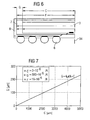
- FIG. 7 shows by way of example a diagram in which the thickness G of the buffer layer over the half semiconductor chip diameter C is plotted.
Landscapes
- Structures For Mounting Electric Components On Printed Circuit Boards (AREA)
- Wire Bonding (AREA)
- Structures Or Materials For Encapsulating Or Coating Semiconductor Devices Or Solid State Devices (AREA)
Description
- Die Erfindung betrifft ein Halbleiterbauelement zur Montage auf einer Leiterplatte, wobei das Halbleiterbauelement ein Gehäuse umfasst, welches Gehäuse wenigstens teilweise umgibt, wobei dem Halbleiterchip elektrische Kontakte zugeordnet sind, vermittels welcher eine elektrische Verbindung mit auf der Leiterplatte vorgesehenen Elektroden oder Elektrodenflächen hergestellt werden soll.
- Aus
US 2002/034872 A1 ist ein Halbleiterbauelement mit einem Gehäuse, einem innenliegenden Chip, der Kontakte an einer Kontaktfläche und eine Abstützfläche aufweist, bekannt. Ferner ist eine Pufferschicht zwischen dem Gehäuse und dem Chip vorgesehen. Weitere Halbleiterbauelemente dieser Gestalt sind aus den DruckschriftenUS 2002/038890 A1 undJP 2001 210760 A - Unter anderem aus der
US 2002/027298 A1 ist es bekannt Halbleiterchips vollständig in ein Gehäuse einzubetten. - Bei hochintegrierten und stark miniaturisierten Halbleiterbauelementen tritt nach deren Montage auf gedruckten Schaltungen (Leiterplatten) verstärkt das Problem auf, dass bei Temperaturschwankungen aufgrund der unterschiedlichen Temperaturausdehnungskoeffizienten der beteiligten Materialen starke mechanische Spannungen innerhalb des Bauelements und zwischen dem Bauelement und der Leiterplatte auftreten.
Figur 4 zeigt eine übliche Bauform eines solchen miniaturisierten Halbleiterbausteins. Das Halbleiterbauelement 1 ist mit seinen elektrischen Kontakten 5 mit der Leiterplatte 2 verbunden. Das Halbleiterchip 3 wiederum ist mittels elektrischer Kontakte 14 mit dem Zwischenstück 12 ("interposer") verbunden, wobei das Halbleiterchip mittels einer Unterfüllung 13 ("underfiller") mit dem Zwischenstück zur mechanischen Stabilisierung verklebt ist. Das Halbleiterchip 3 ist weiterhin mit einer Umhüllung 1 vergossen. Das Zwischenstück 12 ist als Träger auch oftmals vollständig mit vergossen. - Infolge von Temperaturschwankungen oder -veränderungen treten in den bekannten Bauelementformen mechanische Spannungen auf Grund der unterschiedlichen Temperaturausdehnungskoeffizienten der verschiedenen Materialien auf.
Figur 5 verdeutlicht dies näher. Das Halbleiterchip 3 hat einen geringeren Temperaturausdehnungskoeffizienten α als das Zwischenstück 12, das aus einem anderen Material gefertigt ist. Aufgrund der unterschiedlichen Ausdehnung des Halbleiterchips und des Zwischenstücks wird über die zur mechanischen Fixierung und Stabilisierung notwendige Unterfüllung 13 eine starke mechanische Spannung 16 übertragen und in dem Zwischenstück 12 erzeugt. Damit hier nicht ein Verbindungsbruch der elektrischen Kontakte 14 entsteht, muss der Temperaturausdehnungskoeffizient des Zwischenstücks schon an das Halbleiterchip angepasst sein. Üblicherweise Verwendung findende Leiterplatten 2 haben jedoch einen von Halbleiterchips stark unterschiedlichen Temperaturausdehnungskoeffizienten. Daher wird vom, schon unter mechanischer Spannung stehenden, Zwischenstück 12 über die damit strapazierten elektrischen Kontakte 5 eine starke mechanische Spannung 17 auf die Leiterplatte 2 ausgeübt. Im Extremfall kann diese starke mechanische Verspannung zu einer Verformung der Leiterplatte führen, was insbesondere bei einer doppelseitigen Bestückung von Leiterplatten zum Bruch von elektrischen Kontakten 5 und damit zur Zerstörung des elektronischen Gerätes führen kann. Führt die Verformung nicht gleich zum Bruch, dann jedoch im Verlauf von vielen Ver- und Entspannungen zur Ermüdung des Materials der elektrischen Kontakte 5, was dann wieder letztendlich zum Bruch derselben führt und die Lebensdauer begrenzt. Auch führt die starke unterschiedliche Ausdehnung, und damit die mechanische Verspannung, des Halbleiterbauelements in sich selber, also einerseits zwischen Halbleiterchip und Zwischenstück, und Halbleiterchip und Umhüllung - in welcher wieder eine Verspannung 18 induziert wird - andererseits, zur Ermüdung der elektrischen Kontakte 14, wodurch auch eine Zerstörung der elektrischen Kontakte innerhalb der Halbleiterbauelemente 1 erfolgen kann. - Ein direktes Aufsetzen eines Halbleiterchips lediglich über Bumps auf eine Leiterplatte, um mechanische Spannungen oder Übertragungen derselben von dazwischen gelagerten Schichten zu verhindern, führt auch nicht zum Ziel, da hierdurch keine dauerhaft stabile mechanische Verbindung zwischen dem Halbleiterchip und der Leiterplatte erzeugt werden kann. Auch ein Aufkleben eines Chips über Bumps mit einer Unterfüllung ("underfiller"), beispielsweise in Form eines Epoxy-Klebstoffes, würde hier nur die direkten Verspannungen vom Halbleiterchip zur Leiterplatte führen. Hierdurch würde sich die Leiterplatte wiederum verformen, mit den oben genannten Schwierigkeiten. Insbesondere würde es, bei beidseitig bestückten Leiterplatten, zu einer Zerstörung von auf einer Seite einer Leiterplatte befindlichen Schaltungen oder deren elektrischer Kontakte führen.
- Damit dennoch ausreichend langlebige elektronische Schaltungen hergestellt werden können, sind aufwendige und damit teure Gehäusekonstruktionen für Halbleiterbauelemente notewendig.
- Aufgabe der Erfindung ist es daher, ein Halbleiterbauelement zur Verfügung zu stellen, bei denen die oben genannten Nachteile nicht auftreten und bei dem dennoch die sehr kompakte Bauform ermöglicht ist.
- Diese Aufgabe wird durch die kennzeichnenden Merkmale des Anspruchs 1 gelöst.
- Erfindungsgemäß ist vorgesehen, dass das flächige Halbleiterchip eine Montageseitenfläche aufweist, wobei an der Montageseitenfläche elektrische Kontaktflächen zum Kontakt mit den elektrischen Kontakten vorgesehen sind, wobei das Halbleiterchip bis auf eine auf der Montageseitenfläche angeordnete Abstützfläche von einer Pufferschicht umgeben ist, welche sich zwischen dem Gehäuse und der Halbleiterchip befindet, welche Abstützfläche wesentlich kleiner als die Montageseitenfläche ist.
- Die Erfindung schlägt vor, das Halbleiterchip mittels der kleinen Abstützfläche und dem damit geringem räumlichen Kontakt zu Materialien mit ungünstigem Temperaturausdehnungskoeffizienten sozusagen zu entkoppeln, wodurch das Halbleiterchip sich innerhalb des Gehäuses geringer oder mehr ausdehnen kann, als es das umgebende Gehäuse oder die Leiterplatte tut, auf der das Halbleiterbauelement befestigt ist, ohne mechanische Spannungen hervorzurufen. Eine mechanische Stabilisierung des Chips ist dabei in seiner Position auf der Leiterplatte durch das Gehäuse sicher gestellt. Hierdurch wird eine Anpassung an die thermomechanischen Eigenschaften von Leiterplattenmaterial ermöglicht, was eine dauerhafte, verspannungsfreie Verbindung zwischen Leiterplatte (beispielsweise gedruckte Schaltung) und Halbleiterbauelement ermöglicht.
- Eine bevorzugte Ausgestaltung der Erfindung sieht vor, dass das Halbleiterchip sich mechanisch auf einem aus dem Gehäuse ausgeformten Stützsockel auf der auf der Montageseitenfläche angeordneten Abstützfläche abstützt.
- Bevorzugterweise ist das Halbleiterchip mechanisch, fest mit einem aus dem Gehäuse ausgeformten Stützsockel an der auf der Montageseitenfläche angeordneten Abstützfläche verbunden.
- Von Vorteil ist die Abstützfläche zentral in der Montageseitenfläche angeordnet.
- Eine bevorzugte Ausgestaltung der Erfindung sieht vor, das Halbleiterbauelement in WLP- ("wafer level package"), in Flip-Chip- oder in CSP-Bauweise ("chip scale package") gefertigt ist.
- Von Vorteil sind die elektrischen Kontakte durch Bumps ausgebildet.
- Erfindungsgemäß beträgt der Durchmesser G der Pufferschicht zwischen dem Gehäuse einer Seitenfläche des Halbleiterchips

wobei G der Durchmesser der Pufferschicht zwischen dem Gehäuse und einer Seitenfläche des Halbleiterchips ist, C die Länge des Lotes von der Seitenfläche zum Mittelpunkt des Halbleiterchips ist, αC der Temperatur-Ausdehnungskoeffizient des Halbleiterchips ist, αG der Temperatur-Ausdehnungskoeffizient der Pufferschicht ist und αF der Temperatur-Ausdehnungskoeffizient des Gehäuses ist. - Ebenso von Vorteil ist gemäß einer Ausgestaltung der Erfindung vorgesehen, dass das Material der Pufferschicht so gewählt ist, dass der Temperatur-Ausdehnungskoeffizient der Pufferschicht größer als der Temperatur-Ausdehnungskoeffizient von solchem Leiterplattenmaterial ist, auf dem das Halbleiterbauelement befestigt werden soll. Dem folgend ist das Material so gewählt, dass die Pufferschicht den niedrigeren Temperatur-Ausdehnungskoeffizienten vom Halbleitermaterial, beispielsweise Silizium des Halbleiterchips so entspricht, dass beide zusammen dem Temperatur-Ausdehnungskoeffizienten vom Gehäuse bzw. der Leiterplatte entsprechen.
- Dem folgend, ist nach einer Ausgestaltung der Erfindung vorgesehen, dass die Pufferschicht hochelastisch ist.
- Das Material des Gehäuses ist nach einer bevorzugten Ausgestaltung der Erfindung so gewählt ist, dass der Temperatur-Ausdehnungskoeffizient des Gehäuses gleich dem von solchem Leiterplattenmaterial ist, auf dem das Halbleiterbauelement befestigt werden soll.
- Gemäß einer besonders bevorzugten Ausgestaltung der Erfindung ist vorgesehen, dass das Material des Gehäuses so gewählt ist, dass der Temperatur-Ausdehnungskoeffizient des Gehäuses größer als der des Halbleiterchips ist.
- Dem folgend ist gemäß einer Ausgestaltung der Erfindung vorgesehen, dass das Material der Pufferschicht und des Halbleiterchips so gewählt ist, dass deren Temperatur-Ausdehnungskoeffizient zusammen gleich dem des Gehäuses und/oder dem von solchem Leiterplattenmaterial ist, auf dem das Halbleiterbauelement befestigt werden soll.
- Weitere Vorteile, Besonderheiten und zweckmäßige Weiterbildungen der Erfindung ergeben sich aus den weiteren Unteransprüchen oder deren Unterkombinationen.
- Nachfolgend wird die Erfindung anhand der Zeichnung weiter erläutert.
- Dabei zeigt:
- Fig. 1
- ein erfindungsgemäßes Halbleiterbauelement zur Monta- ge auf einer Leiterplatte,
- Fig. 2
- ein erfindungsgemäßes Halbleiterbauelement nach einer zweiten Ausführung,
- Fig. 3
- das Halbleiterbauelement aus
Figur 1 und 2 in Blick- richtung III - Fig. 4
- ein herkömmliches Halbleiterbauelement auf einer Lei- terplatte montiert,
- Fig. 5
- eine schematische Darstellung von Verspannungen eines herkömmlichen Halbleiterbauelements auf einer Leiter- platte,
- Fig. 6
- eine Detailansicht des Halbleiterbauelements aus Fi- gur 1, und
- Fig. 7
- ein Diagramm der Dimensionierung der Elemente der Halbleiterbauelements.
- In den Figuren gleiche Bezugszeichen bezeichnen gleiche oder gleich wirkende Elemente.
- Die
Figur 1 zeigt schematisch ein erfindungsgemäßes Halbleiterbauelement 1 zur Montage auf einer Leiterplatte. Das Halbleiterchip 3 wird dabei vollständig durch das Gehäuse 8 zum Schutz vor Außeneinwirkungen umhüllt. Innerhalb der Gehäuses 8 ist das Halbleiterchip 3 mit einer Pufferschicht 7 bis auf den Bereich der Abstützfläche 31 umgeben. Innerhalb der Abstützfläche 31 ist das Halbleiterchip 3 über elektrische Kontaktflächen 32 über Leitungszuführungen mit den elektrischen Kontakten 5 in Form von Bumps 6 (Lotbällchen, "solder bumps") verbunden, über welche die elektrische Kontaktierung mit den hierzu vorgesehenen Elektrodenflächen auf der Leiterplattenoberfläche der Leiterplatte (nicht dargestellt) erfolgt. - Das Halbleiterchip 3 selbst ist mit dem Gehäuse 8 mechanisch nur durch an der Abstützfläche 31 verbunden. Ansonsten ist das Halbleiterchip weich in der elastischen Pufferschicht gebettet, sodass eine Verspannung mit dem Gehäuse und dadurch bedingte Verformung der Außenmaße des Halbleiterbauelements nicht vorkommen kann.
- Die unterschiedlichen Temperaturausdehnungskoeffizienten α von Halbleiterchip und Leiterplatte führen daher nicht zu Verspannungen, da die unterschiedliche Ausdehnung zwischen Leiterplatte und Halbleiterchip 3 über die ausreichend nachgiebige Pufferschicht 7 abgefangen wird. Die unterschiedliche Ausdehnung zwischen Halbleiterchip 3 und Gehäuse 8 belastet auch nicht mehr die inneren Kotakte 32, da durch die zentrale Anordnung der Kotakte in einem engen Bereich der Gesamtfläche des Chips eine temperaturbedingte Ausdehnung gegenüber dem Gehäuse nicht mehr zu Versetzungen führt. Eine Ermüdung der elektrischen Kontakte im Innern des Halbleiterbauelements wie auch Außen am Halbleiterbauelement wird hierdurch nicht mehr hervorgerufen. Die Lebensdauer ist deutlich erhöht.
-
Figur 2 zeigt ein anderes Ausführungsbeispiel eines Halbleiterbauelements 1, bei dem die elektrischen Kontakte durch sogenannte "Compliant Bumps" 61, also als nachgiebige Bumps ausgebildet sind. Dabei sind die eigentlichen Bumps 61 durch Silikon-Ausformungen gebildet, die im Beispiel zur Kontaktierung mit einem dünnen, hochflexiblen Metallstreifen 6a überzogen sind, um die elektrischen Kontakte zu ermöglichen. -
Figur 3 zeigt eine Ansicht in Blickrichtung III ausFigur 1 und 2 . Die Abstützfläche 31, innerhalb derer sich auch die elektrische Kontaktflächen 32 befinden, ist deutlich kleiner als die Montageseitenfläche 33 und befindet sich in deren Mitte. -
Figur 6 zeigt nochmals detaillierter einen Ausschnitt ausFigur 1 , wobei die Dimensionierung der Schichtdicken nach der Beziehung
bestimmt ist, wobei αC der Temperatur-Ausdehnungskoeffizient des Halbleiterchips ist, αG der Temperatur-Ausdehnungskoeffizient der Pufferschicht 7 ist und αF der Temperatur-Ausdehnungskoeffizient des Gehäuses ist. C ist der Abstand von der Seitenfläche zur Mittelachse 34. Dabei stellt G den minimalen Wert dar. -
Figur 7 zeigt beispielhaft ein Diagramm, in dem die Dicke G der Pufferschicht über dem halben Halbleiterchipdurchmesser C aufgetragen ist. Die Steigung von 4,6 % ergibt sich dabei aus den angenommenen Werten für die Temperatur-Ausdehnungskoeffizienten zu:


-
- 1
- Halbleiterbauelement
- 2
- Leiterplatte
- 3
- Halbleiterchip
- 31
- Abstützfläche
- 32
- elektrische Kontaktfläche
- 33
- Montageseitenfläche
- 34
- Mittelachse
- 4, 8
- Gehäuse
- 5
- elektrische Kontakte
- 6
- Bumps
- 61
- Compliant-Bumps
- 6a
- Metallstreifen
- 7
- Pufferschicht
- 9
- Stützsockel
- 91
- Leitungszuführungen
- 10
- Oberfläche der Leiterplatte
- 12
- Zwischenstück
- 13
- Unterfüllung
- 14
- elektrische Kontakte
- 15
- Umhüllung
- 16 bis 18
- mechanische Spannung
Claims (14)
- Halbleiterbauelement (1) zur Montage auf einer Leiterplatte, wobei das Halbleiterbauelement ein flächig ausgebildetes Halbleiterchip (3) aufweist,
wobei dem Halbleiterchip elektrische Kontakte (5) zugeordnet sind, mittels welcher eine elektrische Verbindung mit auf der Leiterplatte vorgesehenen Elektroden oder Elektrodenflächen hergestellt werden soll,
wobei das flächige Halbleiterchip (3) eine Montageseitenfläche (33) aufweist, wobei auf der Montageseitenfläche (33) eine Abstützfläche (31) angeordnet ist, die wesentlich kleiner als die Montageseitenfläche (33) ist, und innerhalb der Abstützfläche (31) an der Montageseitenfläche (33) elektrische Kontaktflächen (32) zum Kontakt mit den elektrischen Kontakten (5) vorgesehen sind,
wobei das Halbleiterbauelement (1) ein Gehäuse (8) aufweist, wobei das Halbleiterbauelement (1) eine Pufferschicht (7) zwischen dem Gehäuse (8) und dem Halbleiterchip (3) aufweist,
dadurch gekennzeichnet,
dass das Gehäuse (8) das Halbleiterchip (3) vollständig umgibt und die Pufferschicht (7) das Halbleiterchip (3) bis auf den Bereich der Abstützfläche (31) umgibt und
ein Durchmesser G der Pufferschicht (7) zwischen dem Gehäuse (8) einer Seitenfläche des Halbleiterchips (3)
beträgt, wobei G der Durchmesser der Pufferschicht (7) zwischen dem Gehäuse (8) und einer Seitenfläche des Halbleiterchips (3), C die Länge des Lotes von der Seitenfläche zum Mittelpunkt des Halbleiterchips (3), αC der Temperatur-Ausdehnungskoeffizient des Halbleiterchips (3), αG der Temperatur-Ausdehnungskoeffizient der Pufferschicht (7) und αF der Temperatur-Ausdehnungskoeffizient des Gehäuses (8) ist. - Halbleiterbauelement nach Anspruch 1,
dadurch gekennzeichnet,
dass das Halbleiterchip (3) sich mechanisch auf einem aus dem Gehäuse (8) ausgeformten Stützsockel (9) auf der auf der Montageseitenfläche (33) angeordneten Abstützfläche (31) abstützt. - Halbleiterbauelement nach Anspruch 1 oder 2,
dadurch gekennzeichnet,
dass das Halbleiterchip (3) mechanisch fest mit einem aus dem Gehäuse (8) ausgeformten Stützsockel (9) an der auf der Montageseitenfläche (33) angeordneten Abstützfläche (31) verbunden ist und der Sockel zur Zuführung von Leitungszuführungen (91) von den elektrischen Kontakten (5, 6, 61) zu den elektrischen Kontaktflächen (32) dient. - Halbleiterbauelement nach einem der Ansprüche 1 bis 3,
dadurch gekennzeichnet,
dass die Abstützfläche (31) zentral in der Montageseitenfläche (33) angeordnet ist. - Halbleiterbauelement nach einem der Ansprüche 1 bis 3,
dadurch gekennzeichnet,
dass die Abstützfläche (31) am geometrischen Schwerpunkt der Montageseitenfläche (33) angeordnet ist. - Halbleiterbauelement nach einem der vorhergehenden Ansprüche,
dadurch gekennzeichnet,
dass die elektrischen Kontakte (5) durch Bumps (6) ausgebildet sind. - Halbleiterbauelement nach einem der vorhergehenden Ansprüche,
dadurch gekennzeichnet,
dass die Bumps (6) Lotbällchen sind. - Halbleiterbauelement nach einem der Ansprüche 1 bis 6,
dadurch gekennzeichnet,
dass die Bumps (6) Silikonkügelchen mit darüber geführten elektrischen Leitflächen (6a) zur Kontaktierung oder elektrisch leitende im wesentlichen aus Silikon bestehende Kügelchen sind. - Halbleiterbauelement nach einem der vorhergehenden Ansprüche in Verbindung mit einer Leiterplatte,
dadurch gekennzeichnet,
dass das Material der Pufferschicht (7) so gewählt ist, dass der Temperatur-Ausdehnungskoeffizient der Pufferschicht größer als der Temperatur-Ausdehnungskoeffizient von solchem Leiterplattenmaterial ist, auf dem das Halbleiterbauelement (1) befestigt verden soll. - Halbleiterbauelement nach einem der vorhergehenden Ansprüche,
dadurch gekennzeichnet,
dass die Pufferschicht (7) hochelastisch ist. - Halbleiterbauelement nach einem der Ansprüche 9 oder 10, wenn Anspruch 10 sich auf Anspruch 9 rückbezieht,
dadurch gekennzeichnet,
dass das Material des Gehäuses (8) so gewählt ist, dass der Temperatur-Ausdehnungskoeffizient des Gehäuses gleich dem von solchem Leiterplattenmaterial ist, auf dem das Halbleiterbauelement (1) befestigt worden soll. - Halbleiterbauelement nach einem der vorhergehenden Ansprüche,
dadurch gekennzeichnet,
dass das Material des Gehäuses (8) so gewählt ist, dass der Temperatur-Ausdehnungskoeffizient des Gehäuses größer als der des Halbleiterchips (3) ist. - Halbleiterbauelement nach einem der vorhergehenden Ansprüche,
dadurch gekennzeichnet,
dass die Pufferschicht (7) aus einem Polymer, insbesondere Silikon oder Polyurethan besteht. - Halbleiterbauelement nach Anspruch 13,
dadurch gekennzeichnet,
dass die Pufferschicht (7) aus einem aufgeschäumten Material besteht.
Applications Claiming Priority (3)
| Application Number | Priority Date | Filing Date | Title |
|---|---|---|---|
| DE10238581 | 2002-08-22 | ||
| DE10238581A DE10238581B4 (de) | 2002-08-22 | 2002-08-22 | Halbleiterbauelement |
| PCT/EP2003/009227 WO2004019405A1 (de) | 2002-08-22 | 2003-08-20 | Halbleiterbauelement mit csp-gen use |
Publications (2)
| Publication Number | Publication Date |
|---|---|
| EP1530801A1 EP1530801A1 (de) | 2005-05-18 |
| EP1530801B1 true EP1530801B1 (de) | 2010-02-03 |
Family
ID=31501859
Family Applications (1)
| Application Number | Title | Priority Date | Filing Date |
|---|---|---|---|
| EP03792392A Expired - Lifetime EP1530801B1 (de) | 2002-08-22 | 2003-08-20 | Halbleiterbauelement mit csp-gehäuse |
Country Status (5)
| Country | Link |
|---|---|
| US (1) | US7274110B2 (de) |
| EP (1) | EP1530801B1 (de) |
| CN (1) | CN100565852C (de) |
| DE (2) | DE10238581B4 (de) |
| WO (1) | WO2004019405A1 (de) |
Families Citing this family (9)
| Publication number | Priority date | Publication date | Assignee | Title |
|---|---|---|---|---|
| JP3945483B2 (ja) | 2004-01-27 | 2007-07-18 | カシオ計算機株式会社 | 半導体装置の製造方法 |
| DE102004043663B4 (de) * | 2004-09-07 | 2006-06-08 | Infineon Technologies Ag | Halbleitersensorbauteil mit Hohlraumgehäuse und Sensorchip und Verfahren zur Herstellung eines Halbleitersensorbauteils mit Hohlraumgehäuse und Sensorchip |
| DE102006062473A1 (de) | 2006-12-28 | 2008-07-03 | Qimonda Ag | Halbleiterbauelement mit auf einem Substrat montiertem Chip |
| ITMI20070099A1 (it) * | 2007-01-24 | 2008-07-25 | St Microelectronics Srl | Dispositivo elettronico comprendente dispositivi sensori differenziali mems e substrati bucati |
| JP2009049218A (ja) * | 2007-08-21 | 2009-03-05 | Nec Electronics Corp | 半導体装置及び半導体装置の製造方法 |
| CN101488482B (zh) * | 2008-01-18 | 2011-09-14 | 南茂科技股份有限公司 | 半导体封装结构及其制造方法 |
| US7910404B2 (en) * | 2008-09-05 | 2011-03-22 | Infineon Technologies Ag | Method of manufacturing a stacked die module |
| US20160064299A1 (en) * | 2014-08-29 | 2016-03-03 | Nishant Lakhera | Structure and method to minimize warpage of packaged semiconductor devices |
| EP4318564A4 (de) * | 2021-04-29 | 2024-05-22 | Huawei Technologies Co., Ltd. | Leiterplattenbauteil und elektronische vorrichtung |
Family Cites Families (35)
| Publication number | Priority date | Publication date | Assignee | Title |
|---|---|---|---|---|
| JP3105089B2 (ja) * | 1992-09-11 | 2000-10-30 | 株式会社東芝 | 半導体装置 |
| JP2570628B2 (ja) * | 1994-09-21 | 1997-01-08 | 日本電気株式会社 | 半導体パッケージおよびその製造方法 |
| US5783870A (en) * | 1995-03-16 | 1998-07-21 | National Semiconductor Corporation | Method for connecting packages of a stacked ball grid array structure |
| JP3332308B2 (ja) * | 1995-11-07 | 2002-10-07 | 新光電気工業株式会社 | 半導体装置及びその製造方法 |
| US6667560B2 (en) * | 1996-05-29 | 2003-12-23 | Texas Instruments Incorporated | Board on chip ball grid array |
| DE19649798A1 (de) * | 1996-12-02 | 1998-06-04 | Abb Research Ltd | Leistungshalbleitermodul |
| JP3695893B2 (ja) * | 1996-12-03 | 2005-09-14 | 沖電気工業株式会社 | 半導体装置とその製造方法および実装方法 |
| KR100248792B1 (ko) * | 1996-12-18 | 2000-03-15 | 김영환 | 단일층 세라믹 기판을 이용한 칩사이즈 패키지 반도체 |
| KR100237328B1 (ko) * | 1997-02-26 | 2000-01-15 | 김규현 | 반도체 패키지의 구조 및 제조방법 |
| US6235471B1 (en) * | 1997-04-04 | 2001-05-22 | Caliper Technologies Corp. | Closed-loop biochemical analyzers |
| US5881945A (en) * | 1997-04-30 | 1999-03-16 | International Business Machines Corporation | Multi-layer solder seal band for semiconductor substrates and process |
| JP3335575B2 (ja) * | 1997-06-06 | 2002-10-21 | 松下電器産業株式会社 | 半導体装置およびその製造方法 |
| US6014316A (en) * | 1997-06-13 | 2000-01-11 | Irvine Sensors Corporation | IC stack utilizing BGA contacts |
| US6150719A (en) * | 1997-07-28 | 2000-11-21 | General Electric Company | Amorphous hydrogenated carbon hermetic structure and fabrication method |
| DE19803020C2 (de) * | 1998-01-27 | 1999-12-02 | Siemens Ag | Chipkartenmodul für biometrische Sensoren |
| JP2000156435A (ja) * | 1998-06-22 | 2000-06-06 | Fujitsu Ltd | 半導体装置及びその製造方法 |
| JP3602000B2 (ja) * | 1999-04-26 | 2004-12-15 | 沖電気工業株式会社 | 半導体装置および半導体モジュール |
| US6376769B1 (en) * | 1999-05-18 | 2002-04-23 | Amerasia International Technology, Inc. | High-density electronic package, and method for making same |
| DE19931004C2 (de) * | 1999-07-05 | 2002-02-07 | Tyco Electronics Logistics Ag | Chipmodul, insbesondere BGA-Package, mit einem Interconnect zur stressfreien Lötverbindung mit einer Leiterplatte |
| US6441476B1 (en) * | 2000-10-18 | 2002-08-27 | Seiko Epson Corporation | Flexible tape carrier with external terminals formed on interposers |
| DE19954888C2 (de) * | 1999-11-15 | 2002-01-10 | Infineon Technologies Ag | Verpackung für einen Halbleiterchip |
| US6384487B1 (en) * | 1999-12-06 | 2002-05-07 | Micron Technology, Inc. | Bow resistant plastic semiconductor package and method of fabrication |
| JP4374691B2 (ja) * | 2000-01-28 | 2009-12-02 | 凸版印刷株式会社 | チップサイズ型半導体装置 |
| JP2001237351A (ja) * | 2000-02-22 | 2001-08-31 | Hitachi Maxell Ltd | 半導体装置 |
| DE10016132A1 (de) * | 2000-03-31 | 2001-10-18 | Infineon Technologies Ag | Elektronisches Bauelement mit flexiblen Kontaktierungsstellen und Verfahren zu dessen Herstellung |
| US6560117B2 (en) * | 2000-06-28 | 2003-05-06 | Micron Technology, Inc. | Packaged microelectronic die assemblies and methods of manufacture |
| US6326700B1 (en) * | 2000-08-15 | 2001-12-04 | United Test Center, Inc. | Low profile semiconductor package and process for making the same |
| JP2002083904A (ja) * | 2000-09-06 | 2002-03-22 | Sanyo Electric Co Ltd | 半導体装置およびその製造方法 |
| JP3640876B2 (ja) * | 2000-09-19 | 2005-04-20 | 株式会社ルネサステクノロジ | 半導体装置及び半導体装置の実装構造体 |
| JP4183375B2 (ja) * | 2000-10-04 | 2008-11-19 | 沖電気工業株式会社 | 半導体装置及びその製造方法 |
| US6388322B1 (en) * | 2001-01-17 | 2002-05-14 | Aralight, Inc. | Article comprising a mechanically compliant bump |
| DE10133361C2 (de) * | 2001-07-10 | 2003-05-28 | Infineon Technologies Ag | Verfahren zur Herstellung einer Verpackung für Halbleiterchips |
| DE10138278C1 (de) * | 2001-08-10 | 2003-04-03 | Infineon Technologies Ag | Elektronisches Bauteil mit aufeinander gestapelten elektronischen Bauelementen und Verfahren zur Herstellung derselben |
| KR20030029743A (ko) * | 2001-10-10 | 2003-04-16 | 삼성전자주식회사 | 플랙서블한 이중 배선기판을 이용한 적층 패키지 |
| JP4085788B2 (ja) * | 2002-08-30 | 2008-05-14 | 日本電気株式会社 | 半導体装置及びその製造方法、回路基板、電子機器 |
-
2002
- 2002-08-22 DE DE10238581A patent/DE10238581B4/de not_active Expired - Fee Related
-
2003
- 2003-08-20 WO PCT/EP2003/009227 patent/WO2004019405A1/de not_active Ceased
- 2003-08-20 DE DE50312399T patent/DE50312399D1/de not_active Expired - Lifetime
- 2003-08-20 EP EP03792392A patent/EP1530801B1/de not_active Expired - Lifetime
- 2003-08-20 CN CNB038187248A patent/CN100565852C/zh not_active Expired - Fee Related
-
2005
- 2005-02-22 US US11/061,762 patent/US7274110B2/en not_active Expired - Fee Related
Also Published As
| Publication number | Publication date |
|---|---|
| DE50312399D1 (de) | 2010-03-25 |
| CN100565852C (zh) | 2009-12-02 |
| US7274110B2 (en) | 2007-09-25 |
| DE10238581A1 (de) | 2004-03-11 |
| WO2004019405A1 (de) | 2004-03-04 |
| CN1675761A (zh) | 2005-09-28 |
| US20060022338A1 (en) | 2006-02-02 |
| DE10238581B4 (de) | 2008-11-27 |
| EP1530801A1 (de) | 2005-05-18 |
Similar Documents
| Publication | Publication Date | Title |
|---|---|---|
| DE60035667T2 (de) | Kontaktor mit Kontaktelement auf der LSI-Schaltungsseite, Kontaktelement auf der Testplattinenseite zum Testen von Halbleitergeräten und Herstellungsverfahren dafür | |
| DE102007010711B4 (de) | Schaltanordnung, Messvorrichtung damit und Verfahren zu deren Herstellung | |
| DE10131697A1 (de) | Durch eine Basis mit Führung gehaltener Sensor | |
| DE69411535T2 (de) | Bandtest von kontaktmatrix-verbundenen chips | |
| WO2002099845A2 (de) | Elektronischer chip und elektronische chip-anordnung | |
| EP3066722B1 (de) | Elektrische verbindungsanordnung | |
| DE102009001930A1 (de) | Sensorbaustein | |
| EP0237598A1 (de) | Piezoresistives Kraftmesselement sowie dessen Verwendung zur Ermittlung von auf ein Bauteil einwirkenden Kräften | |
| EP2040295A2 (de) | Anordnung mit einer Verbindungseinrichtung und mindestens einem Halbleiterbauelement | |
| DE10238581B4 (de) | Halbleiterbauelement | |
| DE69802146T2 (de) | Umarbeitungsfähige Leiterplattenbestückung mit einem Flip-Chip | |
| DE102004003275B4 (de) | Halbleiterbauteil mit Verbindungselementen auf Halbleiterchips und Verfahren zur Herstellung derselben | |
| DE69517657T2 (de) | Schwingkreisel | |
| DE10297047B4 (de) | Lötfreie Leiterplatten-Baugruppe | |
| DE202004021510U1 (de) | Gehäusestruktur | |
| JP2009222680A (ja) | プローブカード及びプローブカードの製造方法 | |
| DE102004015597B4 (de) | Halbleitervorrichtung mit schützender Gehäusestruktur | |
| EP0383974A1 (de) | Plattenförmiges Sensorelement sowie damit versehener Druck-, Kraft- oder Beschleunigungsaufnehmer | |
| DE102006024652B4 (de) | Bauelement mit TAB-Packung und zugehöriges Herstellungsverfahren | |
| WO2007031298A1 (de) | Flip-chip-modul und verfahren zum erzeugen eines flip-chip-moduls | |
| DE10345395B4 (de) | Halbleitermodul und Verfahren zur Herstellung eines Halbleitermoduls | |
| DE102020119141B4 (de) | Leistungselektronische Schalteinrichtung mit einem Anschlusselement und einer Verbindungseinrichtung | |
| DE102024121567A1 (de) | Elektrischer verbinder montiert auf einem zerbrechlichen substrat | |
| DE102008018793B3 (de) | Anordnung in Druckkontaktausführung mit einem Leistungshalbleitermodul | |
| EP3796373A1 (de) | Platinenanordnung eines implantierbaren medizinischen geräts |
Legal Events
| Date | Code | Title | Description |
|---|---|---|---|
| PUAI | Public reference made under article 153(3) epc to a published international application that has entered the european phase |
Free format text: ORIGINAL CODE: 0009012 |
|
| 17P | Request for examination filed |
Effective date: 20050120 |
|
| AK | Designated contracting states |
Kind code of ref document: A1 Designated state(s): DE FR GB IE IT |
|
| RIN1 | Information on inventor provided before grant (corrected) |
Inventor name: HEDLER, HARRY Inventor name: VASQUEZ, BARBARA Inventor name: MEYER, THORSTEN |
|
| 17Q | First examination report despatched |
Effective date: 20080515 |
|
| RTI1 | Title (correction) |
Free format text: SEMICONDUCTOR COMPONENT HAVING A CSP HOUSING |
|
| GRAJ | Information related to disapproval of communication of intention to grant by the applicant or resumption of examination proceedings by the epo deleted |
Free format text: ORIGINAL CODE: EPIDOSDIGR1 |
|
| GRAP | Despatch of communication of intention to grant a patent |
Free format text: ORIGINAL CODE: EPIDOSNIGR1 |
|
| GRAP | Despatch of communication of intention to grant a patent |
Free format text: ORIGINAL CODE: EPIDOSNIGR1 |
|
| 19U | Interruption of proceedings before grant |
Effective date: 20090903 |
|
| RAP1 | Party data changed (applicant data changed or rights of an application transferred) |
Owner name: QIMONDA AG |
|
| GRAS | Grant fee paid |
Free format text: ORIGINAL CODE: EPIDOSNIGR3 |
|
| 19U | Interruption of proceedings before grant |
Effective date: 20090903 |
|
| 19W | Proceedings resumed before grant after interruption of proceedings |
Effective date: 20091207 |
|
| GRAA | (expected) grant |
Free format text: ORIGINAL CODE: 0009210 |
|
| AK | Designated contracting states |
Kind code of ref document: B1 Designated state(s): DE FR GB IE IT |
|
| REG | Reference to a national code |
Ref country code: GB Ref legal event code: FG4D Free format text: NOT ENGLISH |
|
| REG | Reference to a national code |
Ref country code: IE Ref legal event code: FG4D |
|
| REF | Corresponds to: |
Ref document number: 50312399 Country of ref document: DE Date of ref document: 20100325 Kind code of ref document: P |
|
| REG | Reference to a national code |
Ref country code: IE Ref legal event code: FD4D |
|
| PG25 | Lapsed in a contracting state [announced via postgrant information from national office to epo] |
Ref country code: IE Free format text: LAPSE BECAUSE OF FAILURE TO SUBMIT A TRANSLATION OF THE DESCRIPTION OR TO PAY THE FEE WITHIN THE PRESCRIBED TIME-LIMIT Effective date: 20100203 |
|
| PLBE | No opposition filed within time limit |
Free format text: ORIGINAL CODE: 0009261 |
|
| STAA | Information on the status of an ep patent application or granted ep patent |
Free format text: STATUS: NO OPPOSITION FILED WITHIN TIME LIMIT |
|
| 26N | No opposition filed |
Effective date: 20101104 |
|
| PG25 | Lapsed in a contracting state [announced via postgrant information from national office to epo] |
Ref country code: IT Free format text: LAPSE BECAUSE OF FAILURE TO SUBMIT A TRANSLATION OF THE DESCRIPTION OR TO PAY THE FEE WITHIN THE PRESCRIBED TIME-LIMIT Effective date: 20100203 |
|
| REG | Reference to a national code |
Ref country code: DE Ref legal event code: R081 Ref document number: 50312399 Country of ref document: DE Owner name: INFINEON TECHNOLOGIES AG, DE Free format text: FORMER OWNER: QIMONDA AG, 81739 MUENCHEN, DE Ref country code: DE Ref legal event code: R081 Ref document number: 50312399 Country of ref document: DE Owner name: POLARIS INNOVATIONS LTD., IE Free format text: FORMER OWNER: QIMONDA AG, 81739 MUENCHEN, DE |
|
| REG | Reference to a national code |
Ref country code: GB Ref legal event code: 732E Free format text: REGISTERED BETWEEN 20150827 AND 20150902 |
|
| REG | Reference to a national code |
Ref country code: FR Ref legal event code: PLFP Year of fee payment: 13 |
|
| REG | Reference to a national code |
Ref country code: DE Ref legal event code: R081 Ref document number: 50312399 Country of ref document: DE Owner name: POLARIS INNOVATIONS LTD., IE Free format text: FORMER OWNER: INFINEON TECHNOLOGIES AG, 85579 NEUBIBERG, DE |
|
| PGFP | Annual fee paid to national office [announced via postgrant information from national office to epo] |
Ref country code: GB Payment date: 20150923 Year of fee payment: 13 |
|
| PGFP | Annual fee paid to national office [announced via postgrant information from national office to epo] |
Ref country code: FR Payment date: 20151008 Year of fee payment: 13 |
|
| REG | Reference to a national code |
Ref country code: FR Ref legal event code: TP Owner name: INFINEON TECHNOLOGIES AG, DE Effective date: 20160212 |
|
| GBPC | Gb: european patent ceased through non-payment of renewal fee |
Effective date: 20160820 |
|
| REG | Reference to a national code |
Ref country code: FR Ref legal event code: ST Effective date: 20170428 |
|
| PG25 | Lapsed in a contracting state [announced via postgrant information from national office to epo] |
Ref country code: GB Free format text: LAPSE BECAUSE OF NON-PAYMENT OF DUE FEES Effective date: 20160820 Ref country code: FR Free format text: LAPSE BECAUSE OF NON-PAYMENT OF DUE FEES Effective date: 20160831 |
|
| PGFP | Annual fee paid to national office [announced via postgrant information from national office to epo] |
Ref country code: DE Payment date: 20170815 Year of fee payment: 15 |
|
| REG | Reference to a national code |
Ref country code: DE Ref legal event code: R119 Ref document number: 50312399 Country of ref document: DE |
|
| PG25 | Lapsed in a contracting state [announced via postgrant information from national office to epo] |
Ref country code: DE Free format text: LAPSE BECAUSE OF NON-PAYMENT OF DUE FEES Effective date: 20190301 |