EP1528402A1 - Magnetischer sensor - Google Patents
Magnetischer sensor Download PDFInfo
- Publication number
- EP1528402A1 EP1528402A1 EP04771810A EP04771810A EP1528402A1 EP 1528402 A1 EP1528402 A1 EP 1528402A1 EP 04771810 A EP04771810 A EP 04771810A EP 04771810 A EP04771810 A EP 04771810A EP 1528402 A1 EP1528402 A1 EP 1528402A1
- Authority
- EP
- European Patent Office
- Prior art keywords
- current
- sensitive member
- magnetic
- detection coil
- magnetic sensor
- Prior art date
- Legal status (The legal status is an assumption and is not a legal conclusion. Google has not performed a legal analysis and makes no representation as to the accuracy of the status listed.)
- Granted
Links
Images


Classifications
-
- G—PHYSICS
- G01—MEASURING; TESTING
- G01R—MEASURING ELECTRIC VARIABLES; MEASURING MAGNETIC VARIABLES
- G01R33/00—Arrangements or instruments for measuring magnetic variables
- G01R33/02—Measuring direction or magnitude of magnetic fields or magnetic flux
- G01R33/06—Measuring direction or magnitude of magnetic fields or magnetic flux using galvano-magnetic devices
- G01R33/09—Magnetoresistive devices
-
- G—PHYSICS
- G01—MEASURING; TESTING
- G01R—MEASURING ELECTRIC VARIABLES; MEASURING MAGNETIC VARIABLES
- G01R33/00—Arrangements or instruments for measuring magnetic variables
- G01R33/02—Measuring direction or magnitude of magnetic fields or magnetic flux
-
- G—PHYSICS
- G01—MEASURING; TESTING
- G01R—MEASURING ELECTRIC VARIABLES; MEASURING MAGNETIC VARIABLES
- G01R33/00—Arrangements or instruments for measuring magnetic variables
- G01R33/02—Measuring direction or magnitude of magnetic fields or magnetic flux
- G01R33/06—Measuring direction or magnitude of magnetic fields or magnetic flux using galvano-magnetic devices
- G01R33/063—Magneto-impedance sensors; Nanocristallin sensors
Definitions
- the present invention relates to magnetic sensors for measuring weak magnetic fields with high precision.
- a magnetic sensor having a coil wound around an amorphous wire is known as one conventional magnetic sensor including a magneto-impedance element.
- a method of extracting the first pulse of an oscillation waveform induced in a coil when a pulse current with a rise time of 5 nanoseconds is passed through an amorphous wire is used in order to obtain a voltage that sensitively varies in proportion to an external magnetic field H ex (see, for example, Patent Document 1).
- Patent Document 1 discloses that a feedback coil is wound around an amorphous wire, a feedback circuit is provided, and a negative-feedback current proportional to a sensor output voltage is continuously passed through the feedback coil so as to perform a negative feedback, so that a magnetic sensor exhibiting high-precision characteristics with high linearity and no hysteresis is realized.
- Patent Document 1 Japanese Unexamined Patent Application Publication No. 2000-258517
- the known magnetic sensor has the following problems: that is, in order to improve the precision of the magnetic sensor, the feedback circuit, as previously mentioned, is required, for example. Therefore, the circuitry becomes complex and the magnetic sensor may be large. On the other hand, if the feedback circuit is omitted, for example, the magnetic sensor may lack precision.
- a magnetic sensor includes a magnetic sensitive member whose electromagnetic characteristics vary by the action of an external magnetic field; a driving circuit for supplying a current to the magnetic sensitive member; a detection coil wound around the magnetic sensitive member; and a sample-and-hold circuit for measuring an induced voltage value which is the magnitude of voltage induced in the detection coil, wherein the sample-and-hold circuit is configured to measure the induced voltage value in synchronization with an interruption of the current performed by the driving circuit.
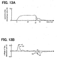
- FIGs. 13A and 13B show how a magnetic detection unit, in which a detection coil is wound around an amorphous wire, operates when an external magnetic field is +2 gauss (G).
- Fig. 13A illustrates one example of a current waveform used to drive the amorphous wire, in which a current-carrying time of 35 nanoseconds (ns) is repeated at predetermined intervals.
- Fig. 13B illustrates voltages induced in the detection coil. For example, when a pulse current rises as shown in Fig. 13A, a positive damped oscillation voltage Q1 as shown in Fig. 13B is present in the detection coil, whereas when a pulse current falls, a negative damped oscillation voltage Q2 is present.
- the magnitude and polarity of the damped oscillation voltage are determined vectorially depending on the relationship between the magnitude of the external magnetic field and the angle between the direction of the external magnetic field and the axial direction of the amorphous wire. As a result, the magnitude of the external magnetic field can be determined from the damped oscillation voltage.
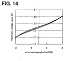
- a peak voltage value p1 which is the maximum value of the damped oscillation voltage induced in the detection coil when the pulse current rises, varies as shown in Fig. 14.
- a method for measuring an external magnetic field by measuring the voltage p1 when the pulse current rises is unsuitable for direction measurement requiring high precision.
- the inventors of the present invention have carried out intensive research on the relationship in magnitude (see Figs. 13A and 13B) between the voltage induced in the detection coil and the external magnetic field when the amorphous wire is driven by the pulse current, and based on the results obtained, the inventors have conceived the invention described below.
- the present invention is characterized by comprising a magnetic sensitive member including an amorphous wire through which a pulse current can pass; a detection coil wound around the magnetic sensitive member; and a sample-and-hold circuit for detecting a voltage induced in the detection coil in synchronization with an interruption of the pulse current.
- the damped oscillation voltage Q2 which is induced in the detection coil by the change in current when the pulse current passing through the amorphous wire falls by an interruption, is detected by the sample-and-hold circuit.
- the circuitry can be simplified, so that the magnetic sensor can be miniaturized and reduced in profile.
- omitting the feedback circuit, which requires a current continuously passing therethrough, can suppress power consumption.
- the sample-and-hold circuit may be configured to measure the first peak value in time in a damped oscillation waveform of the induced voltage value, the damped oscillation waveform varying with time in response to the interruption of the current.
- a peak value p2 in the damped oscillation voltage Q2 can be detected, so that the magnetic sensor can have high precision.
- the sample-and-hold circuit may comprise timing-retaining means for retaining a predetermined timing in response to the interruption of the current performed by the driving circuit, and the sample-and-hold circuit is configured to measure the induced voltage value in synchronization with the interruption of the current with the predetermined timing, wherein the predetermined timing is equal to a timing at which the induced voltage value in damped oscillation exhibits the first zero-crossing in time in the interruption of the current passing through the magnetic sensitive member held in the external magnetic field whose intensity is substantially zero.
- the zero crossing herein refers to polarity inversion, in which a positive (negative) value is inverted to a negative (positive) value in the induced voltage value in damped oscillation.
- the timing at which the induced voltage value in damped oscillation exhibits a zero crossing is the timing at which the induced voltage value generated in the detection coil independently of the external magnetic field becomes zero.
- the timing at which the induced voltage value in damped oscillation exhibits the first zero-crossing in time is retained as the predetermined timing and the external magnetic field is measured by operating the sample-and-hold circuit in synchronization with interruption at this the predetermined timing.
- a voltage component generated independently of the external magnetic field due to electromagnetic induction between the detection coil and the magnetic sensitive member or the like is less prone to being contained as an error component. Therefore, according to the magnetic sensor, the induced voltage value generated by the action of the external magnetic field can be measured with high precision.
- the timing-retaining means may be, for example, a delay circuit in which a coil, a resistor, and a capacitor are selectively combined.
- the timing-retaining means may use a timer capability of a microcomputer.
- the driving circuit may comprise voltage-retaining means for retaining a minimum voltage value being the induced voltage value measured by the sample-and-hold circuit when the external magnetic field having a minimum magnetic field intensity detected by the magnetic sensor acts on the magnetic sensitive member; and the driving circuit is configured to interrupt the current in a state in which the induced voltage value converges within a voltage range equal to or less than 5% of the minimum voltage value.
- the induced voltage value In a state in which the induced voltage value converges in the voltage range, when the current is interrupted, the induced voltage value can be measured afterwards with high precision by using the sample-and-hold circuit.
- the state in which the induced voltage value converges in the voltage range refers to a state in which the damped oscillation voltage induced in the detection coil in response to a rise of the current stays within the voltage range.
- the voltage-retaining means may be such that the induced voltage value is input to an envelope detecting circuit in which a diode and a CR circuit are combined and the convergence is measured by comparing an output voltage value from the envelope detecting circuit with a threshold value.
- the voltage-retaining means may be such that a second sample-and-hold circuit for sampling and holding a peak value of the induced voltage value is added and the convergence is measured by comparing a voltage measured by the second sample-and-hold circuit and a threshold value.
- the driving circuit may be configure so that a pulse current variation serving as the current acts on the magnetic sensitive member; and a rise time required to raise the magnitude of the current up to a predetermined current value is set to be from 3 to 30 times an interruption time to interrupt the current at the predetermined current value.
- setting the rise time to be 3 or more times the interruption time can strongly suppress the induced voltage value resulting from the rise of the current, as compared with the induced voltage value resulting from the interruption of the current. Suppressing the induced voltage value during this rise can control relative effects on the induced voltage value to be measured, and thus, the measurement precision of the magnetic sensor can be improved.
- the rise time refers to the time required for the current to rise from 10% to 90% of a predetermined current value.
- the interruption time refers to the time required for the current to fall from 90% to 10% of the predetermined current value.
- the predetermined current value refers to the magnitude of the current when interrupted.
- the driving circuit may comprise a capacitor storing electric energy serving as a supply source of the current and an electronic switch arranged in an electrical path between the capacitor and the magnetic sensitive member; and the current supplied from the capacitor to the magnetic sensitive member is interrupted by the use of the electronic switch.
- the use of the driving circuit including the capacitor and the electronic switch allows the rate of change of current to become large, so that the detectivity of the magnetic sensor can be further improved.
- the magnetic sensor may further comprises an electrode wiring board having a groove extending in one direction, the groove filled with an insulator having an electrical insulating property, wherein the magnetic sensitive member is an amorphous wire arranged so as to pass through the insulator along the groove direction of the groove; and the detection coil has a spiral electrical path in which a first coil unit arranged on a groove surface being an inner surface of the groove and a second coil unit arranged on a groove top being an outer surface of the insulator are combined.
- the magnetic sensor has the structure in which the detection coil, which has the first coil unit formed on the inner surface of the groove and the second coil unit formed on the top face of the groove in combination, and the amorphous wire, which passes through the insulator in the groove, are combined. Therefore, the miniaturization of the magnetic sensor can be realized.
- a magnetic sensor used to measure direction in, for example, a small electronic device, such as a cellular phone or personal digital assistant be miniaturized and reduced in profile.
- the magnetic sensor described above sufficiently meets the requirements and specifications with respect to size required for the miniaturization or the reduction in profile.
- the magnetic sensitive member may be an amorphous wire having a diameter from 1 ⁇ m to 30 ⁇ m; and the detection coil has a winding inner diameter equal to or less than 200 ⁇ m.
- winding inner diameter is set to be equal to or less than 200 ⁇ m. If the gap is reduced, excitation obtained from the skin effect in the magnetic sensitive member including the amorphous wire can be effectively utilized. As a consequence, the induced voltage value in the detection coil can be large, so that a high-sensitivity magnetic sensor can be realized.
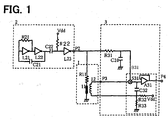
- Embodiment 1 of the present invention will be described with reference to Figs. 1, 2, 13A, and 13B.
- Fig. 1 is a schematic circuit diagram of a magnetic sensor according to this embodiment.
- a magnetic detection unit 1 is composed of a zero-magnetostriction amorphous wire 11 having a length of 2.5 mm and a diameter of 30 ⁇ m, serving as a magnetic sensitive member, and being made out of a CoFeSiB-based alloy; a detection coil 12 consisting of 40 turns wound around the amorphous wire 11; and a current controlling resistor R11.
- the amorphous wire 11 is connected to an output terminal P2 of a pulse generator 2 via the resistor R11 so as to allow a pulse current to pass therethrough.
- the detection coil 12 is connected to an input terminal P3 of an electronic switch of a sample-and-hold circuit 3 so as to output a voltage based on an induced voltage generated in accordance with an external magnetic field when the pulse current is interrupted.
- the pulse generator 2 is composed of a multivibrator including complementary MOS (CMOS) inverter elements L21 and L22, a resistor R21, and a capacitor C21; and a wave-shaping circuit including a CMOS inverter element L23 and a differentiating circuit having a capacitor C22 and a resistor R22.
- CMOS complementary MOS
- the wave-shaping circuit is electrically connected to the multivibrator.
- the wave-shaping circuit repeatedly generates a pulse voltage in which a time period of a logic level "1" is 35 nanoseconds (ns) at 1 MHz when the multivibrator generates a rectangular wave having a frequency of 1 MHz, and outputs the pulse voltages to the output terminal P2.
- the sample-and-hold circuit 3 is composed of a sample-and-hold unit B31 including an electronic switch S31, a capacitor C32, a resistor R32, a resistor R33, and a high-input-resistance amplifier A31; and a delay circuit including a resistor R31 and a capacitor C31 connected to a control terminal of the electronic switch S31.
- the other terminal of the delay circuit is connected to the output terminal P2 of the pulse generator.
- the delay circuit sets a logic level of the control terminal of the electronic switch S31 at "1" with a predetermined delay time determined by the resistor R31 and the capacitor C31.
- the electronic switch S31 is changed to the "closed” state and the induced voltage in the detection coil 12 is applied to the capacitor C32. Then, when the pulse in the output terminal P2 falls, the current passing through the amorphous wire 11 is interrupted and the electronic switch S31 is changed to the "open” state after a predetermined time interval ⁇ t determined by the resistor R31 and the capacitor C31.
- this delay time ⁇ t is adjusted to the time from when the current passing through the amorphous wire 11 is interrupted (time t1) to when the peak value p2, which is the maximum value of the damped oscillation voltage Q2, appears in the detection coil 12 (time t2). Therefore, the electronic switch S31 is changed to the "open” state substantially in synchronization with the timing of the appearance of the peak value p2.
- the capacitor C32 holds a voltage that is applied to the detection coil immediately before the electronic switch S31 is changed to the "open" state.
- the high-input-resistance amplifier A31 converts the voltage in the detection coil into a direct-current voltage so as to output a voltage that corresponds to the magnitude of the external magnetic field to an output terminal P4, and continues outputting until the next pulse in repeated pulses at 1 MHz updates it.
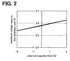
- Fig. 2 shows results obtained when the magnetic field applied to the magnetic detection unit is varied in the range of ⁇ 3G.
- This drawing illustrates results obtained when a voltage of the peak value p2, which is the maximum value of the damped oscillation voltage Q2 induced in the detection coil 12 when the pulse current is interrupted, is converted to a direct-current voltage by the sample-and-hold circuit.
- the nonlinearity and hysteresis are both equal to or less than 2%, and therefore, the precision reaches practical levels for direction measurement.
- the magnetic sensor circuit according to this embodiment it is not necessary for the magnetic sensor circuit according to this embodiment to have a negative-feedback circuit. This eliminates the need for continuously passing a negative-feedback current through the negative-feedback circuit, so that low power consumption can be realized.
- the magnetic sensor according to this embodiment achieves the following advantages:
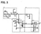
- Embodiment 2 of the present invention will now be described with reference to Figs. 3 to 5, 13A, and 13B.
- Fig. 3 is a schematic circuit diagram of the magnetic sensor according to this embodiment.
- a driving circuit 4 for supplying a pulse current to the amorphous wire 11 is added to the circuit diagram of Fig. 1.
- Other circuits shown in Fig. 3 are the same as those in Fig. 1, so the driving circuit 4 will be described below.
- the driving circuit 4 is composed of a capacitor C41 charged by a voltage Vdd (connected to an unshown stabilized power supply circuit); an electronic switch S41; and a delay circuit including a resistor R41 and a capacitor C42.
- the driving circuit 4 supplies a current to the resistor R11 and the amorphous wire 11 of the magnetic detection unit 1 from the capacitor C41 when the electronic switch S41 is in the "closed" state.
- the delay circuit including the resistor R41 and the capacitor C42 is used to adjust the operation timing of the electronic switch S31 in response to an interruption of the current passing through the amorphous wire 11.
- the delay time in the delay circuit is set such that the electronic switch S31 of the sample-and-hold circuit is changed to the "open" state at the timing at which the damped oscillation voltage induced in the detection coil 12 becomes a peak value.
- the operation of switching between "closed” and “open” states performed by the electronic switch S41 is quicker than that by a CMOS inverter element, and moreover, the electronic switch S41 allows a large current to pass. Therefore, the rate of change of current with respect to the rise time and the fall time of a pulse current passing through the amorphous wire 11 can be large.
- Fig. 4A shows current movements in the amorphous wire 11 when a pulse current (35 ns) is passed through the amorphous wire 11.
- Fig. 4B shows voltage movements in the detection coil.
- a gradient k2 which expresses the rate of change of current when the pulse current in the amorphous wire 11 is interrupted, is nearly twice as much as a gradient k1 shown in Fig. 13A, in which the CMOS inverter element performs driving. Therefore, the magnitude of a peak value p3 of the damped oscillation voltage induced in the detection coil 12 is nearly twice the peak value p2 as shown in Fig. 13B.
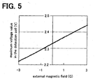
- Fig. 5 shows the peak value p3 of the damped oscillation voltage induced in the detection coil when an external magnetic field acting on the magnetic detection unit 1 varies in the range of ⁇ 3G.
- the sensitivity i.e., the output voltage per unit magnetic field intensity is 0.037 V/G. This is approximately 2.5 times a sensitivity of 0.015 V/G in embodiment 1, as shown in Fig. 2.
- the driving circuit 4 to supply a pulse current to the amorphous wire 11 is added.
- the driving circuit 4 passes and interrupts a current supplied from the charged capacitor to the magnetic sensitive member by the use of its electronic switch. Therefore, the rate of change of a pulse current passing through the amorphous wire can be large, so that the precision of the magnetic sensor can be further improved.
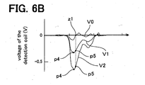
- Fig. 6A shows variations in pulse current supplied to the amorphous wire 11 when the pulse current is interrupted.
- Fig. 6B shows variations in voltage induced in the detection coil of the magnetic detection unit (the reference numeral 1 in Fig. 1).
- the reference numeral V0 represents the variations in voltage when an external magnetic field acting on the magnetic detection unit is substantially zero.
- the reference numeral V1 represents the variations in voltage when the magnetic field intensity of the external magnetic field acting in the axial direction of the amorphous wire of the magnetic detection unit is 1 G.
- the reference numeral V2 represents the variations in voltage when the magnetic field intensity of the external magnetic field acting in the axial direction of the amorphous wire of the magnetic detection unit is 2 G.
- the voltage induced in the detection coil would be constantly zero.
- V0 a damped oscillation voltage having a small amplitude is produced in the detection coil due to electromagnetic induction between the amorphous wire and the detection coil or the like.
- This damped oscillation voltage V0 induced in the detection coil due to electromagnetic induction between the amorphous wire and the detection coil or the like is likely to be superimposed on the damped oscillation voltage V1 or V2 used to measure the external magnetic field.
- the voltage produced resulting from the electromagnetic induction between the amorphous wire and the detection coil or the like is likely to be a cause of measurement error in the magnetic sensor.
- the delay time in the delay circuit according to embodiment 1 is set to the time from when the current passing through the amorphous wire 11 is interrupted to when the first zero-crossing z1 in the damped oscillation voltage V0 appears in the detection coil, as shown in Figs. 1 and 6B. Therefore, the electronic switch S31 is changed to the "open” state at the timing at which this first zero-crossing z1 appears.
- the capacitor C32 holds a voltage that is applied to the detection coil immediately before the electronic switch S31 is changed to the "open" state.
- the high-input-resistance amplifier converts the voltage in the detection coil into a direct-current voltage, thereby outputting a voltage corresponding to the magnitude of the external magnetic field to the output terminal P4.
- the delay time in the delay circuit matches the timing at which the zero-crossing z1 (see Fig. 6B) of the damped oscillation voltage in the detection coil appears where the external magnetic field is substantially zero. Therefore, in the measurement of the external magnetic field by the magnetic sensor in this embodiment, an error due to electromagnetic induction between the amorphous wire and the detection coil or the like can be suppressed. Additionally, the delay time matches the first zero-crossing z1 in time. Therefore, when this delay time is set, a voltage value p5 whose magnitude is close to the peak voltage p4 can be measured as a voltage in the detection coil, as shown in Fig. 6B.
- an error due to electromagnetic induction between the amorphous wire and the detection coil or the like can be suppressed. This results in high-precision measurement.
- an inductance L41 is connected between the capacitor C41 and the electronic switch S41.
- This driving circuit 4 can generate a sawtooth current due to the first-order lag characteristics resulting from a time constant determined by the inductance L41 and the resistor R11 when the electronic switch S41 is changed to the "closed" state.
- a diode D41 is connected in parallel with the inductance L41. The diode D41 absorbs a surge voltage when the electronic switch S41 is changed to the "open" state.
- the driving circuit 4 can generate a sawtooth current having a gentle rise when the electronic switch S41 is changed to the "closed” state, i.e., when a current passing through the amorphous wire rises.
- the electronic switch S41 is changed to the "open” state, i.e., when the current passing through the amorphous wire is interrupted, the current can fall sharply, as compared with the rise described above.
- a pulse current that is close to a sawtooth current is supplied to the amorphous wire.
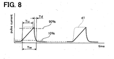
- the rise time, Tu is set to 20 ns and the interruption time, Td, is set to 3 ns.
- the rise time Tu in this embodiment is approximately 7 times the interruption time Td.
- the passage time, Tw, from the rise to the interruption is set to about 25 ns.
- the rise time Tu refers to the time required for the current to rise from 10% to 90% of its steady-state value.
- the interruption time Td refers to the time required for the current to fall from 90% to 10% of its steady-state value.
- the passage time Tw is determined so as to satisfy the following requirement: that is, the requirement is that the magnitude of the damped oscillation voltage induced in the detection coil associated with the rise of the current converges in a voltage range equal to or less than 5% of a minimum voltage value, which will be described later.
- the minimum voltage value refers to the magnitude of the induced voltage value measured by the sample-and-hold circuit when the external magnetic field having the minimum magnetic field intensity detected by the magnetic sensor acts on the magnetic sensitive member.
- the driving circuit 4 passes a current rising gently at the time of passing the pulse current through the amorphous wire. Therefore, as compared with when a pulse current that is close to perfect is supplied (shown by a dotted line d1), power consumption can be reduced and the energy-saving effects can be achieved. Moreover, when the rate of change of current at the time of the current passing through the amorphous wire to rise is made smaller (the current rises gently), the amplitude of the oscillation voltage produced in the detection coil can be suppressed. If the current passing through the amorphous wire is interrupted in a state in which the amplitude of the oscillation voltage in the detection coil is small, the voltage generated in accordance with the external magnetic field can be measured with high precision. In other words, since the oscillation voltage resulting from the rise of the current converges promptly, interrupting the current immediately so as to measure the external magnetic field is allowed. As a result, the passage time can be reduced and the energy-saving effects can be achieved.
- the sawtooth current is used.
- an imperfect pulse current having a longer rise time relative to the interruption time may be used.
- This imperfect pulse current can be realized by adjusting the time constant in the driving circuit 4 of this embodiment. For example, if the rise time is set to be from 3 to 30 times the interruption time, the advantages in this embodiment are achieved.
- a magneto-impedance element including the magnetic detection unit having an amorphous wire through which a pulse current can be passed and a detection coil wound around the magnetic sensitive member will now be described with reference to Figs. 9 to 12.
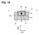
- an insulating member 40 is disposed between a magnetic sensitive member 20 for detecting a magnetic field and a detection coil 30 on an electrode wiring board 10.
- the detection coil 30 having a winding inner diameter equal to or less than 200 ⁇ m is arranged around the insulating member 40. Terminals of the magnetic sensitive member 20 and the detection coil 30 are connected to their respective electrodes 51 and 52 on the electrode wiring board 10.
- the magneto-impedance element passes a pulse current through the magnetic sensitive member 20 via the electrodes 51 and 52 and outputs a voltage generated at that time in the detection coil 30.
- the winding inner diameter of the detection coil 30 is reduced to 200 ⁇ m or less.
- the winding inner diameter herein refers to a circle-equivalent diameter, which is equal to a diameter of a circle having the same area as a cross-sectional area defined by the height and width of a groove shown in Fig. 10. If the winding inner diameter is enlarged, a gap between the magnetic sensitive member and the detection coil is increased, thus failing to realize high sensitivity. It is desired that the magneto-impedance element be miniaturized. In view of these circumstances, the winding inner diameter is 200 ⁇ m or less in this embodiment.
- the magnetic sensitive member 20 is a conductive magnetic amorphous wire made out of a CoFeSiB-based alloy and having a diameter of 10 to 30 ⁇ m. It is preferable that the diameter of the magnetic amorphous wire be 10 to 30 ⁇ m in terms of manufacturability.
- the electrode wiring board 10 has a groove 90 having a depth of 40 to 200 ⁇ m.
- a detection coil portion 31 (a first coil unit 31) is arranged on a groove surface 91, and a detection coil portion 32 (a second coil unit 32) is arranged on a groove top 92 of the groove.
- the detection coil 30 has a two-tier structure consisting of the first coil unit 31 and the second coil unit 32.
- the dimensions of the electrode wiring board 10 in this embodiment are 0.5 mm wide by 0.5 mm high by 1.5 mm long.
- the magnetic sensitive member is the amorphous wire 20 made out of a CoFeSiB-based alloy and having a diameter of 20 ⁇ m.
- the dimensions of the groove 90 are 50 ⁇ m deep by 70 ⁇ m wide by 1.5 mm long.
- the detection coil 30 has a two-tier structure consisting of the first coil unit 31 formed on the groove surface 91 and the second coil unit 32 formed on the groove top 92.
- the first coil unit 31 formed on the groove surface 91 is formed by selectively removing a thin conductive metal layer formed by vapor deposition over the entire area of the groove surface 91 of the groove 90 and the adjacent area to the groove 90 on the top surface of the electrode wiring board 10. Specifically, the first coil unit 31 has interstices in spaces in the spiral thin metal layer by the use of selective etching so that the thin metal layer in the shape of a spiral remains.
- a plurality of coil strips 311 which are vertically arranged, are disposed in the groove direction.
- Each of the coil strips 312 connect a first segment of the coil strip 311 to a third segment of the coil strip 311 facing a second segment of the coil strip 311 adjacent to the first segment of the coil strip 311 in the groove direction. Therefore, the first coil unit 31 having the coil strips 311 and 312 in combination takes the form of a spiral as a whole.
- the second coil unit 32 formed on the groove top 92 (the second coil unit 32 formed on a top face 41 of the insulating resin member 40) comprises a thin conductive metal layer formed by vapor deposition over a wide area including the groove top 92 in the longitudinal direction of the electrode wiring board 10.
- the second coil unit 32 is formed by the application of selective etching to this thin metal layer. Specifically, portions of the metal thin layer are removed by selective etching so that a plurality of thin metal layer strips arranged along the width direction of the groove 90 is formed.
- the second coil unit 32 is formed so as to connect the coil strips 311 facing each other together.
- a protective layer may be formed if needed.
- the winding inner diameter of the detection coil 30 in this embodiment is 66 ⁇ m in circle-equivalent diameter.
- the detection coil has a winding spacing of 50 ⁇ m and has 20 turns.
- a gap between the amorphous wire 20 and the detection coil 30 is filled with the insulating resin member 40, so that the conductive magnetic amorphous wire 20 is kept electrically insulated from the detection coil 30.
- the size of the magneto-impedance element in this embodiment is substantially the same as that of the electrode wiring board.
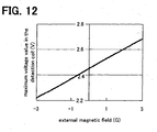
- the magneto-impedance element is evaluated by the use of the circuit diagram (see Fig. 3) in embodiment 2.
- Fig. 12 shows the results. As is apparent from Fig. 12, a sensitivity of 0.076 V/G, superior to the sensitivity (see Fig. 5) realized in embodiment 2, is achieved.
- the average gap between the amorphous wire and the detection coil in the magneto-impedance element is 23 ⁇ m, whereas that used in the magneto-impedance element of a known type according to embodiment 2 is approximately 1 mm.
- Fig. 15 shows one example thereof.
- the dimensions of a substrate 110 are 1.0 mm wide by 0.5 mm high by 2.5 mm long.
- an amorphous wire 120 made out of a CoFeSiB-based alloy and having a diameter of 30 ⁇ m is protected by a gelling resin member.
- a detection coil 130 is wound around the amorphous wire 120.
- An insulating winding frame 160 and electrodes 150 are provided. Accordingly, the high sensitivity (0.076 V/G) is realized by a reduction in gap between the amorphous wire serving as the magnetic sensitive member and the detection coil for detecting the output.
- the miniaturized magneto-impedance element allows the magnetic sensor to be miniaturized and reduced in profile.
Landscapes
- Physics & Mathematics (AREA)
- Condensed Matter Physics & Semiconductors (AREA)
- General Physics & Mathematics (AREA)
- Chemical & Material Sciences (AREA)
- Engineering & Computer Science (AREA)
- Nanotechnology (AREA)
- Measuring Magnetic Variables (AREA)
- Hall/Mr Elements (AREA)
Applications Claiming Priority (3)
| Application Number | Priority Date | Filing Date | Title |
|---|---|---|---|
| JP2003208682 | 2003-08-25 | ||
| JP2003208682 | 2003-08-25 | ||
| PCT/JP2004/011849 WO2005019851A1 (ja) | 2003-08-25 | 2004-08-18 | 磁気センサ |
Publications (3)
| Publication Number | Publication Date |
|---|---|
| EP1528402A1 true EP1528402A1 (de) | 2005-05-04 |
| EP1528402A4 EP1528402A4 (de) | 2008-07-16 |
| EP1528402B1 EP1528402B1 (de) | 2011-08-10 |
Family
ID=34208996
Family Applications (1)
| Application Number | Title | Priority Date | Filing Date |
|---|---|---|---|
| EP04771810A Expired - Lifetime EP1528402B1 (de) | 2003-08-25 | 2004-08-18 | Magnetischer sensor |
Country Status (7)
| Country | Link |
|---|---|
| US (1) | US7026812B2 (de) |
| EP (1) | EP1528402B1 (de) |
| JP (1) | JP3801194B2 (de) |
| KR (1) | KR100666292B1 (de) |
| CN (1) | CN1697980B (de) |
| TW (1) | TWI285747B (de) |
| WO (1) | WO2005019851A1 (de) |
Cited By (2)
| Publication number | Priority date | Publication date | Assignee | Title |
|---|---|---|---|---|
| EP2276082A4 (de) * | 2008-03-28 | 2012-01-25 | Aichi Steel Corp | Magnetempfindlicher draht, magnetimpedanzelement und magnetimpedanzsensor |
| EP2725375A4 (de) * | 2011-06-22 | 2016-01-13 | Canon Denshi Kk | Magnetfelderkennungsverfahren und magnetfelderkennungsschaltung |
Families Citing this family (42)
| Publication number | Priority date | Publication date | Assignee | Title |
|---|---|---|---|---|
| KR100825762B1 (ko) | 2006-08-07 | 2008-04-29 | 한국전자통신연구원 | 금속-절연체 전이(mit) 소자의 불연속 mit를연속적으로 측정하는 회로 및 그 회로를 이용한 mit센서 |
| EP1901421A1 (de) * | 2006-09-13 | 2008-03-19 | ABB Schweiz AG | Verfahren zum Bestimmen der Rotorwinkelposition einer rotierenden elektrischen Maschine |
| US7755352B1 (en) | 2007-01-26 | 2010-07-13 | Northrop Grumman Systems Corporation | Built-in testing and transient avoidance for magnetic sensors |
| EP2199814B1 (de) * | 2007-10-02 | 2012-12-12 | Aichi Steel Corporation | Magnetimpedanzelement und magnetimpedanzsensor |
| JP4979554B2 (ja) * | 2007-11-30 | 2012-07-18 | 株式会社フジクラ | 磁気センサを用いた外部磁界の測定方法 |
| JP4725600B2 (ja) * | 2008-06-10 | 2011-07-13 | 愛知製鋼株式会社 | マグネトインピーダンスセンサ素子 |
| CN101674085B (zh) * | 2008-09-10 | 2011-12-21 | 中国科学院半导体研究所 | 一种应用于模数转换器的采样保持电路 |
| TWI383155B (zh) * | 2009-04-21 | 2013-01-21 | China Steel Corp | Measurement device for non - sine wave electromagnetic properties |
| JP5429717B2 (ja) | 2011-03-07 | 2014-02-26 | 国立大学法人名古屋大学 | 磁気検出装置 |
| CN102155968B (zh) * | 2011-03-08 | 2012-02-22 | 陈益华 | 电磁推敲式物体检测装置 |
| US9817078B2 (en) * | 2012-05-10 | 2017-11-14 | Allegro Microsystems Llc | Methods and apparatus for magnetic sensor having integrated coil |
| WO2014115765A1 (ja) | 2013-01-25 | 2014-07-31 | マグネデザイン株式会社 | 磁気検出装置 |
| JP6281677B2 (ja) | 2013-03-08 | 2018-02-21 | 国立大学法人名古屋大学 | 磁気計測装置 |
| US10725100B2 (en) | 2013-03-15 | 2020-07-28 | Allegro Microsystems, Llc | Methods and apparatus for magnetic sensor having an externally accessible coil |
| US10495699B2 (en) | 2013-07-19 | 2019-12-03 | Allegro Microsystems, Llc | Methods and apparatus for magnetic sensor having an integrated coil or magnet to detect a non-ferromagnetic target |
| US10145908B2 (en) | 2013-07-19 | 2018-12-04 | Allegro Microsystems, Llc | Method and apparatus for magnetic sensor producing a changing magnetic field |
| JP2016057190A (ja) | 2014-09-10 | 2016-04-21 | 愛知製鋼株式会社 | 磁界測定装置 |
| US9823092B2 (en) | 2014-10-31 | 2017-11-21 | Allegro Microsystems, Llc | Magnetic field sensor providing a movement detector |
| JP5839527B1 (ja) | 2015-02-16 | 2016-01-06 | マグネデザイン株式会社 | 超高感度マイクロ磁気センサ |
| JP6398830B2 (ja) | 2015-03-26 | 2018-10-03 | 愛知製鋼株式会社 | 磁気インピーダンスセンサ |
| JP6210084B2 (ja) | 2015-04-21 | 2017-10-11 | 愛知製鋼株式会社 | 高精度測定可能な磁気インピーダンスセンサ用感磁ワイヤの製造方法 |
| CN105425008B (zh) * | 2015-10-30 | 2018-06-12 | 张良 | 物联网高灵敏度磁性传感器采样电路 |
| JP5991634B1 (ja) * | 2015-12-18 | 2016-09-14 | マグネデザイン株式会社 | 磁気検出装置 |
| CN112609605A (zh) | 2016-02-10 | 2021-04-06 | 爱知制钢株式会社 | 辊体 |
| SG11201806864UA (en) | 2016-02-16 | 2018-09-27 | Aichi Steel Corp | Work vehicle system and magnetic marker work method |
| US10012518B2 (en) | 2016-06-08 | 2018-07-03 | Allegro Microsystems, Llc | Magnetic field sensor for sensing a proximity of an object |
| JP7012421B2 (ja) | 2016-06-17 | 2022-01-28 | 愛知製鋼株式会社 | 磁気マーカ及びマーカシステム |
| US11428755B2 (en) | 2017-05-26 | 2022-08-30 | Allegro Microsystems, Llc | Coil actuated sensor with sensitivity detection |
| US10837943B2 (en) | 2017-05-26 | 2020-11-17 | Allegro Microsystems, Llc | Magnetic field sensor with error calculation |
| US10996289B2 (en) | 2017-05-26 | 2021-05-04 | Allegro Microsystems, Llc | Coil actuated position sensor with reflected magnetic field |
| US10823586B2 (en) | 2018-12-26 | 2020-11-03 | Allegro Microsystems, Llc | Magnetic field sensor having unequally spaced magnetic field sensing elements |
| US20200256930A1 (en) * | 2019-02-11 | 2020-08-13 | Spincoil Systems, Inc. | Current-sensing method of gmi magnetic field measurement |
| US11237020B2 (en) | 2019-11-14 | 2022-02-01 | Allegro Microsystems, Llc | Magnetic field sensor having two rows of magnetic field sensing elements for measuring an angle of rotation of a magnet |
| US11280637B2 (en) | 2019-11-14 | 2022-03-22 | Allegro Microsystems, Llc | High performance magnetic angle sensor |
| US11262422B2 (en) | 2020-05-08 | 2022-03-01 | Allegro Microsystems, Llc | Stray-field-immune coil-activated position sensor |
| JP7295516B2 (ja) | 2020-12-23 | 2023-06-21 | 国立研究開発法人産業技術総合研究所 | 磁気センサ及び生体磁気計測装置 |
| US11493361B2 (en) | 2021-02-26 | 2022-11-08 | Allegro Microsystems, Llc | Stray field immune coil-activated sensor |
| JP7476829B2 (ja) | 2021-03-19 | 2024-05-01 | 株式会社デンソー | 磁気検出システム |
| US11578997B1 (en) | 2021-08-24 | 2023-02-14 | Allegro Microsystems, Llc | Angle sensor using eddy currents |
| JP7740300B2 (ja) * | 2023-05-26 | 2025-09-17 | 株式会社豊田中央研究所 | 磁気計測装置の製造方法及び磁気計測装置 |
| WO2025134776A1 (ja) * | 2023-12-21 | 2025-06-26 | 愛知製鋼株式会社 | 磁気センサ装置 |
| US12523717B2 (en) | 2024-02-15 | 2026-01-13 | Allegro Microsystems, Llc | Closed loop magnetic field sensor with current control |
Family Cites Families (17)
| Publication number | Priority date | Publication date | Assignee | Title |
|---|---|---|---|---|
| US3991361A (en) * | 1975-03-27 | 1976-11-09 | Westinghouse Electric Corporation | Semi-automatic compass calibrator apparatus for a vehicle mounted flux gate compass system to cancel out effect of local magnetic disturbances |
| EP0074219B1 (de) * | 1981-09-09 | 1985-11-27 | EMI Limited | Anordnung zum Auflösen magnetischer Feldkomponenten |
| DE3843087C2 (de) * | 1987-12-21 | 2001-09-13 | Tdk Corp | Magnetfeldsensor |
| JP3126642B2 (ja) * | 1995-11-09 | 2001-01-22 | 科学技術振興事業団 | 磁界センサ |
| JP3091413B2 (ja) * | 1996-06-11 | 2000-09-25 | 科学技術振興事業団 | 磁気センサ |
| JPH1164473A (ja) * | 1997-08-22 | 1999-03-05 | Sumitomo Metal Mining Co Ltd | 磁気センサ及び磁気方位センサ |
| US6229307B1 (en) * | 1998-08-12 | 2001-05-08 | Minebea Co., Ltd. | Magnetic sensor |
| JP4418040B2 (ja) * | 1998-10-01 | 2010-02-17 | アルプス電気株式会社 | 磁気センサ |
| JP3645116B2 (ja) | 1999-03-10 | 2005-05-11 | 独立行政法人科学技術振興機構 | 磁気インピーダンス効果マイクロ磁気センサ |
| JP2001133529A (ja) * | 1999-11-05 | 2001-05-18 | Aichi Steel Works Ltd | 磁気インピーダンスセンサの感磁アモルファス体支持構造 |
| JP2001296127A (ja) * | 2000-04-13 | 2001-10-26 | Aichi Steel Works Ltd | 磁場検出装置 |
| JP2002247749A (ja) * | 2001-02-16 | 2002-08-30 | Fuji Electric Co Ltd | 過負荷電流保安装置 |
| JP2002318250A (ja) * | 2001-02-16 | 2002-10-31 | Fuji Electric Co Ltd | 電流検出装置およびこれを用いた過負荷電流保安装置 |
| JP3572457B2 (ja) * | 2001-10-12 | 2004-10-06 | アイチ・マイクロ・インテリジェント株式会社 | 磁気検出装置 |
| EP1336858A3 (de) * | 2002-02-19 | 2005-03-23 | Aichi Micro Intelligent Corporation | Zweidimensionaler Magnetfeldsensor |
| WO2003071299A1 (en) * | 2002-02-19 | 2003-08-28 | Aichi Steel Corporation | Magnet with electromagnetic coil/impedance/sensor element |
| JP3786887B2 (ja) * | 2002-03-04 | 2006-06-14 | アイチ・マイクロ・インテリジェント株式会社 | 磁気検出器 |
-
2004
- 2004-08-18 JP JP2005513288A patent/JP3801194B2/ja not_active Expired - Fee Related
- 2004-08-18 WO PCT/JP2004/011849 patent/WO2005019851A1/ja not_active Ceased
- 2004-08-18 EP EP04771810A patent/EP1528402B1/de not_active Expired - Lifetime
- 2004-08-18 US US10/522,753 patent/US7026812B2/en not_active Expired - Lifetime
- 2004-08-18 CN CN2004800004469A patent/CN1697980B/zh not_active Expired - Lifetime
- 2004-08-18 KR KR1020047020438A patent/KR100666292B1/ko not_active Expired - Fee Related
- 2004-08-26 TW TW093125575A patent/TWI285747B/zh not_active IP Right Cessation
Cited By (4)
| Publication number | Priority date | Publication date | Assignee | Title |
|---|---|---|---|---|
| EP2276082A4 (de) * | 2008-03-28 | 2012-01-25 | Aichi Steel Corp | Magnetempfindlicher draht, magnetimpedanzelement und magnetimpedanzsensor |
| US8610427B2 (en) | 2008-03-28 | 2013-12-17 | Aichi Steel Corporation | Magneto-sensitive wire, magneto-impedance element and magneto-impedance sensor |
| CN103454601B (zh) * | 2008-03-28 | 2016-05-18 | 爱知制钢株式会社 | 磁敏线、磁阻抗元件及磁阻抗传感器 |
| EP2725375A4 (de) * | 2011-06-22 | 2016-01-13 | Canon Denshi Kk | Magnetfelderkennungsverfahren und magnetfelderkennungsschaltung |
Also Published As
| Publication number | Publication date |
|---|---|
| US20060038561A1 (en) | 2006-02-23 |
| EP1528402A4 (de) | 2008-07-16 |
| JP3801194B2 (ja) | 2006-07-26 |
| CN1697980A (zh) | 2005-11-16 |
| KR100666292B1 (ko) | 2007-01-11 |
| TWI285747B (en) | 2007-08-21 |
| CN1697980B (zh) | 2010-04-28 |
| JPWO2005019851A1 (ja) | 2006-10-19 |
| KR20060025113A (ko) | 2006-03-20 |
| US7026812B2 (en) | 2006-04-11 |
| EP1528402B1 (de) | 2011-08-10 |
| TW200510749A (en) | 2005-03-16 |
| WO2005019851A1 (ja) | 2005-03-03 |
Similar Documents
| Publication | Publication Date | Title |
|---|---|---|
| EP1528402B1 (de) | Magnetischer sensor | |
| US9543947B2 (en) | Semiconductor device | |
| JP3078843B2 (ja) | 低電力磁力計回路 | |
| JP4319970B2 (ja) | 静電容量式近接センサ | |
| CN111585244B (zh) | 漏电保护电路、集成电路、电子设备以及方法 | |
| JP2018087782A (ja) | 直流漏電検出装置、漏電検出装置 | |
| JP5991634B1 (ja) | 磁気検出装置 | |
| US6384596B1 (en) | Variable inductance transducer circuit producing an electrical current and voltage output | |
| JP2025032272A (ja) | 磁気抵抗弛張発振器磁力計 | |
| JP2001116814A (ja) | 磁気インピーダンス素子 | |
| JP2018200242A (ja) | 電流センサ | |
| TWI297777B (en) | Voltage-frequency conversion device and reference voltage changing method of the same | |
| JP5685102B2 (ja) | チャージアンプ | |
| WO2012176451A1 (ja) | 磁界検出方法及び磁界検出回路 | |
| US6768296B2 (en) | Circuit arrangement for generating square pulses and improved compensation current sensor using same | |
| WO2007138791A1 (ja) | アナログ絶縁マルチプレクサ | |
| JP2001343402A (ja) | 直流電流検出器 | |
| JP2014219488A (ja) | セラミックデバイス及びその動作方法 | |
| Jobling | New open-loop current transducers with near closed-loop performance | |
| JP4090829B2 (ja) | 周波数変調形磁界センサー | |
| JPH1151975A (ja) | ロゴスキーコイル用積分回路 | |
| JP2611631B2 (ja) | ピークホールド回路 | |
| JP5806604B2 (ja) | 磁場検出回路 | |
| RU2310271C1 (ru) | Преобразователь тока в частоту импульсов | |
| JPH03117912A (ja) | パルス発生回路 |
Legal Events
| Date | Code | Title | Description |
|---|---|---|---|
| PUAI | Public reference made under article 153(3) epc to a published international application that has entered the european phase |
Free format text: ORIGINAL CODE: 0009012 |
|
| 17P | Request for examination filed |
Effective date: 20050228 |
|
| AK | Designated contracting states |
Kind code of ref document: A1 Designated state(s): AT BE BG CH CY CZ DE DK EE ES FI FR GB GR HU IE IT LI LU MC NL PL PT RO SE SI SK TR |
|
| AX | Request for extension of the european patent |
Extension state: AL HR LT LV MK |
|
| DAX | Request for extension of the european patent (deleted) | ||
| RBV | Designated contracting states (corrected) |
Designated state(s): DE GB |
|
| A4 | Supplementary search report drawn up and despatched |
Effective date: 20080612 |
|
| RIC1 | Information provided on ipc code assigned before grant |
Ipc: G01R 33/09 20060101ALI20080606BHEP Ipc: G01R 33/02 20060101AFI20050308BHEP |
|
| 17Q | First examination report despatched |
Effective date: 20081030 |
|
| GRAP | Despatch of communication of intention to grant a patent |
Free format text: ORIGINAL CODE: EPIDOSNIGR1 |
|
| GRAS | Grant fee paid |
Free format text: ORIGINAL CODE: EPIDOSNIGR3 |
|
| GRAA | (expected) grant |
Free format text: ORIGINAL CODE: 0009210 |
|
| RAP1 | Party data changed (applicant data changed or rights of an application transferred) |
Owner name: AICHI STEEL CORPORATION |
|
| RIN1 | Information on inventor provided before grant (corrected) |
Inventor name: SUMI, KAZUMASA,C/O AICHI STEEL CORPORATION Inventor name: YAMAMOTO, MICHIHARU,C/O AICHI STEEL CORPORATION Inventor name: MORI, MASAKI,C/O AICHI STEEL CORPORATION Inventor name: KOUTANI, YOSHIAKI,C/O AICHI STEEL CORPORATION Inventor name: HONKURA, YOSHINOBU,C/O AICHI STEEL CORPORATION |
|
| AK | Designated contracting states |
Kind code of ref document: B1 Designated state(s): DE GB |
|
| REG | Reference to a national code |
Ref country code: GB Ref legal event code: FG4D |
|
| REG | Reference to a national code |
Ref country code: DE Ref legal event code: R096 Ref document number: 602004033895 Country of ref document: DE Effective date: 20111006 |
|
| PLBE | No opposition filed within time limit |
Free format text: ORIGINAL CODE: 0009261 |
|
| STAA | Information on the status of an ep patent application or granted ep patent |
Free format text: STATUS: NO OPPOSITION FILED WITHIN TIME LIMIT |
|
| 26N | No opposition filed |
Effective date: 20120511 |
|
| REG | Reference to a national code |
Ref country code: DE Ref legal event code: R097 Ref document number: 602004033895 Country of ref document: DE Effective date: 20120511 |
|
| P01 | Opt-out of the competence of the unified patent court (upc) registered |
Effective date: 20230413 |
|
| PGFP | Annual fee paid to national office [announced via postgrant information from national office to epo] |
Ref country code: GB Payment date: 20230824 Year of fee payment: 20 |
|
| PGFP | Annual fee paid to national office [announced via postgrant information from national office to epo] |
Ref country code: DE Payment date: 20230821 Year of fee payment: 20 |
|
| REG | Reference to a national code |
Ref country code: DE Ref legal event code: R071 Ref document number: 602004033895 Country of ref document: DE |
|
| REG | Reference to a national code |
Ref country code: GB Ref legal event code: PE20 Expiry date: 20240817 |
|
| PG25 | Lapsed in a contracting state [announced via postgrant information from national office to epo] |
Ref country code: GB Free format text: LAPSE BECAUSE OF EXPIRATION OF PROTECTION Effective date: 20240817 |
|
| PG25 | Lapsed in a contracting state [announced via postgrant information from national office to epo] |
Ref country code: GB Free format text: LAPSE BECAUSE OF EXPIRATION OF PROTECTION Effective date: 20240817 |