EP1524706B1 - Methode zum Herstellen einer organischen elektrolumineszenten Vorrichtung - Google Patents
Methode zum Herstellen einer organischen elektrolumineszenten Vorrichtung Download PDFInfo
- Publication number
- EP1524706B1 EP1524706B1 EP04024610.0A EP04024610A EP1524706B1 EP 1524706 B1 EP1524706 B1 EP 1524706B1 EP 04024610 A EP04024610 A EP 04024610A EP 1524706 B1 EP1524706 B1 EP 1524706B1
- Authority
- EP
- European Patent Office
- Prior art keywords
- layer
- organic
- electrode layer
- anode electrode
- light
- Prior art date
- Legal status (The legal status is an assumption and is not a legal conclusion. Google has not performed a legal analysis and makes no representation as to the accuracy of the status listed.)
- Active
Links
- 238000004519 manufacturing process Methods 0.000 title claims description 12
- 238000002347 injection Methods 0.000 claims description 125
- 239000007924 injection Substances 0.000 claims description 125
- GNTDGMZSJNCJKK-UHFFFAOYSA-N divanadium pentaoxide Chemical compound O=[V](=O)O[V](=O)=O GNTDGMZSJNCJKK-UHFFFAOYSA-N 0.000 claims description 58
- 150000002894 organic compounds Chemical class 0.000 claims description 50
- 238000000034 method Methods 0.000 claims description 47
- -1 arylamine compound Chemical class 0.000 claims description 36
- 229910044991 metal oxide Inorganic materials 0.000 claims description 34
- 150000004706 metal oxides Chemical class 0.000 claims description 33
- IBHBKWKFFTZAHE-UHFFFAOYSA-N n-[4-[4-(n-naphthalen-1-ylanilino)phenyl]phenyl]-n-phenylnaphthalen-1-amine Chemical compound C1=CC=CC=C1N(C=1C2=CC=CC=C2C=CC=1)C1=CC=C(C=2C=CC(=CC=2)N(C=2C=CC=CC=2)C=2C3=CC=CC=C3C=CC=2)C=C1 IBHBKWKFFTZAHE-UHFFFAOYSA-N 0.000 claims description 32
- 238000000151 deposition Methods 0.000 claims description 28
- 239000000758 substrate Substances 0.000 claims description 26
- 238000004544 sputter deposition Methods 0.000 claims description 16
- 238000003475 lamination Methods 0.000 claims description 14
- 238000007740 vapor deposition Methods 0.000 claims description 12
- 238000012546 transfer Methods 0.000 claims description 11
- 238000006479 redox reaction Methods 0.000 claims description 10
- 150000005839 radical cations Chemical class 0.000 claims description 8
- 150000005838 radical anions Chemical class 0.000 claims description 4
- MQRCTQVBZYBPQE-UHFFFAOYSA-N 189363-47-1 Chemical compound C1=CC=CC=C1N(C=1C=C2C3(C4=CC(=CC=C4C2=CC=1)N(C=1C=CC=CC=1)C=1C=CC=CC=1)C1=CC(=CC=C1C1=CC=C(C=C13)N(C=1C=CC=CC=1)C=1C=CC=CC=1)N(C=1C=CC=CC=1)C=1C=CC=CC=1)C1=CC=CC=C1 MQRCTQVBZYBPQE-UHFFFAOYSA-N 0.000 claims description 3
- 230000009477 glass transition Effects 0.000 claims description 3
- 238000010438 heat treatment Methods 0.000 claims description 3
- ZDAWFMCVTXSZTC-UHFFFAOYSA-N 2-n',7-n'-dinaphthalen-1-yl-2-n',7-n'-diphenyl-9,9'-spirobi[fluorene]-2',7'-diamine Chemical compound C1=CC=CC=C1N(C=1C2=CC=CC=C2C=CC=1)C1=CC=C(C=2C(=CC(=CC=2)N(C=2C=CC=CC=2)C=2C3=CC=CC=C3C=CC=2)C23C4=CC=CC=C4C4=CC=CC=C43)C2=C1 ZDAWFMCVTXSZTC-UHFFFAOYSA-N 0.000 claims description 2
- 229910019571 Re2O7 Inorganic materials 0.000 claims description 2
- 125000002029 aromatic hydrocarbon group Chemical group 0.000 claims description 2
- IEQIEDJGQAUEQZ-UHFFFAOYSA-N phthalocyanine Chemical class N1C(N=C2C3=CC=CC=C3C(N=C3C4=CC=CC=C4C(=N4)N3)=N2)=C(C=CC=C2)C2=C1N=C1C2=CC=CC=C2C4=N1 IEQIEDJGQAUEQZ-UHFFFAOYSA-N 0.000 claims description 2
- 230000002093 peripheral effect Effects 0.000 claims 3
- 238000010894 electron beam technology Methods 0.000 claims 1
- 239000010410 layer Substances 0.000 description 392
- 229910052751 metal Inorganic materials 0.000 description 41
- 239000002184 metal Substances 0.000 description 41
- 230000015572 biosynthetic process Effects 0.000 description 31
- 150000001875 compounds Chemical class 0.000 description 19
- 229910052782 aluminium Inorganic materials 0.000 description 18
- XAGFODPZIPBFFR-UHFFFAOYSA-N aluminium Chemical compound [Al] XAGFODPZIPBFFR-UHFFFAOYSA-N 0.000 description 16
- 239000011521 glass Substances 0.000 description 16
- 238000000295 emission spectrum Methods 0.000 description 15
- 238000012360 testing method Methods 0.000 description 14
- 238000000862 absorption spectrum Methods 0.000 description 11
- 230000004888 barrier function Effects 0.000 description 11
- 230000008021 deposition Effects 0.000 description 10
- 239000012044 organic layer Substances 0.000 description 10
- 239000007772 electrode material Substances 0.000 description 9
- 230000008569 process Effects 0.000 description 9
- 239000000523 sample Substances 0.000 description 8
- 239000011777 magnesium Substances 0.000 description 7
- 150000002739 metals Chemical class 0.000 description 7
- 239000002841 Lewis acid Substances 0.000 description 6
- AMGQUBHHOARCQH-UHFFFAOYSA-N indium;oxotin Chemical compound [In].[Sn]=O AMGQUBHHOARCQH-UHFFFAOYSA-N 0.000 description 6
- 238000005259 measurement Methods 0.000 description 6
- 229910021645 metal ion Inorganic materials 0.000 description 6
- 238000006722 reduction reaction Methods 0.000 description 6
- 229910052709 silver Inorganic materials 0.000 description 6
- 238000011156 evaluation Methods 0.000 description 5
- 229910052749 magnesium Inorganic materials 0.000 description 5
- 230000003287 optical effect Effects 0.000 description 5
- 230000009467 reduction Effects 0.000 description 5
- WHXSMMKQMYFTQS-UHFFFAOYSA-N Lithium Chemical compound [Li] WHXSMMKQMYFTQS-UHFFFAOYSA-N 0.000 description 4
- FYYHWMGAXLPEAU-UHFFFAOYSA-N Magnesium Chemical compound [Mg] FYYHWMGAXLPEAU-UHFFFAOYSA-N 0.000 description 4
- BQCADISMDOOEFD-UHFFFAOYSA-N Silver Chemical compound [Ag] BQCADISMDOOEFD-UHFFFAOYSA-N 0.000 description 4
- 230000000694 effects Effects 0.000 description 4
- 230000005684 electric field Effects 0.000 description 4
- 238000005516 engineering process Methods 0.000 description 4
- 229910052744 lithium Inorganic materials 0.000 description 4
- 125000002524 organometallic group Chemical group 0.000 description 4
- 239000004332 silver Substances 0.000 description 4
- UHOVQNZJYSORNB-UHFFFAOYSA-N Benzene Chemical compound C1=CC=CC=C1 UHOVQNZJYSORNB-UHFFFAOYSA-N 0.000 description 3
- 229910045601 alloy Inorganic materials 0.000 description 3
- 239000000956 alloy Substances 0.000 description 3
- 238000011161 development Methods 0.000 description 3
- 230000003467 diminishing effect Effects 0.000 description 3
- 239000000463 material Substances 0.000 description 3
- 239000000203 mixture Substances 0.000 description 3
- 239000002245 particle Substances 0.000 description 3
- 229910052761 rare earth metal Inorganic materials 0.000 description 3
- 239000000126 substance Substances 0.000 description 3
- TVIVIEFSHFOWTE-UHFFFAOYSA-K tri(quinolin-8-yloxy)alumane Chemical compound [Al+3].C1=CN=C2C([O-])=CC=CC2=C1.C1=CN=C2C([O-])=CC=CC2=C1.C1=CN=C2C([O-])=CC=CC2=C1 TVIVIEFSHFOWTE-UHFFFAOYSA-K 0.000 description 3
- 241000284156 Clerodendrum quadriloculare Species 0.000 description 2
- KWYHDKDOAIKMQN-UHFFFAOYSA-N N,N,N',N'-tetramethylethylenediamine Chemical compound CN(C)CCN(C)C KWYHDKDOAIKMQN-UHFFFAOYSA-N 0.000 description 2
- 229910001420 alkaline earth metal ion Inorganic materials 0.000 description 2
- 150000004982 aromatic amines Chemical class 0.000 description 2
- 239000000872 buffer Substances 0.000 description 2
- XCJYREBRNVKWGJ-UHFFFAOYSA-N copper(II) phthalocyanine Chemical compound [Cu+2].C12=CC=CC=C2C(N=C2[N-]C(C3=CC=CC=C32)=N2)=NC1=NC([C]1C=CC=CC1=1)=NC=1N=C1[C]3C=CC=CC3=C2[N-]1 XCJYREBRNVKWGJ-UHFFFAOYSA-N 0.000 description 2
- ZUOUZKKEUPVFJK-UHFFFAOYSA-N diphenyl Chemical compound C1=CC=CC=C1C1=CC=CC=C1 ZUOUZKKEUPVFJK-UHFFFAOYSA-N 0.000 description 2
- 229910052745 lead Inorganic materials 0.000 description 2
- 229910000476 molybdenum oxide Inorganic materials 0.000 description 2
- UHVLDCDWBKWDDN-UHFFFAOYSA-N n-phenyl-n-[4-[4-(n-pyren-2-ylanilino)phenyl]phenyl]pyren-2-amine Chemical group C1=CC=CC=C1N(C=1C=C2C=CC3=CC=CC4=CC=C(C2=C43)C=1)C1=CC=C(C=2C=CC(=CC=2)N(C=2C=CC=CC=2)C=2C=C3C=CC4=CC=CC5=CC=C(C3=C54)C=2)C=C1 UHVLDCDWBKWDDN-UHFFFAOYSA-N 0.000 description 2
- 239000011368 organic material Substances 0.000 description 2
- 230000027756 respiratory electron transport chain Effects 0.000 description 2
- 229910001925 ruthenium oxide Inorganic materials 0.000 description 2
- WOCIAKWEIIZHES-UHFFFAOYSA-N ruthenium(iv) oxide Chemical compound O=[Ru]=O WOCIAKWEIIZHES-UHFFFAOYSA-N 0.000 description 2
- 238000001228 spectrum Methods 0.000 description 2
- 229910052718 tin Inorganic materials 0.000 description 2
- 229910001935 vanadium oxide Inorganic materials 0.000 description 2
- LQRAULANJCQXAM-UHFFFAOYSA-N 1-n,5-n-dinaphthalen-1-yl-1-n,5-n-diphenylnaphthalene-1,5-diamine Chemical compound C1=CC=CC=C1N(C=1C2=CC=CC(=C2C=CC=1)N(C=1C=CC=CC=1)C=1C2=CC=CC=C2C=CC=1)C1=CC=CC2=CC=CC=C12 LQRAULANJCQXAM-UHFFFAOYSA-N 0.000 description 1
- STTGYIUESPWXOW-UHFFFAOYSA-N 2,9-dimethyl-4,7-diphenyl-1,10-phenanthroline Chemical compound C=12C=CC3=C(C=4C=CC=CC=4)C=C(C)N=C3C2=NC(C)=CC=1C1=CC=CC=C1 STTGYIUESPWXOW-UHFFFAOYSA-N 0.000 description 1
- MVLOINQUZSPUJS-UHFFFAOYSA-N 2-n,2-n,6-n,6-n-tetrakis(4-methylphenyl)naphthalene-2,6-diamine Chemical compound C1=CC(C)=CC=C1N(C=1C=C2C=CC(=CC2=CC=1)N(C=1C=CC(C)=CC=1)C=1C=CC(C)=CC=1)C1=CC=C(C)C=C1 MVLOINQUZSPUJS-UHFFFAOYSA-N 0.000 description 1
- MATLFWDVOBGZFG-UHFFFAOYSA-N 2-n,2-n,6-n,6-n-tetranaphthalen-1-ylnaphthalene-2,6-diamine Chemical compound C1=CC=C2C(N(C=3C=C4C=CC(=CC4=CC=3)N(C=3C4=CC=CC=C4C=CC=3)C=3C4=CC=CC=C4C=CC=3)C=3C4=CC=CC=C4C=CC=3)=CC=CC2=C1 MATLFWDVOBGZFG-UHFFFAOYSA-N 0.000 description 1
- DJIXFCSAUCLVLK-UHFFFAOYSA-N 2-n,2-n,6-n,6-n-tetranaphthalen-2-yl-9h-fluorene-2,6-diamine Chemical compound C1=CC=CC2=CC(N(C=3C=C4C=CC=CC4=CC=3)C3=CC=C4CC5=CC(=CC=C5C4=C3)N(C=3C=C4C=CC=CC4=CC=3)C=3C=C4C=CC=CC4=CC=3)=CC=C21 DJIXFCSAUCLVLK-UHFFFAOYSA-N 0.000 description 1
- VXJRNCUNIBHMKV-UHFFFAOYSA-N 2-n,6-n-dinaphthalen-1-yl-2-n,6-n-dinaphthalen-2-ylnaphthalene-2,6-diamine Chemical compound C1=CC=C2C(N(C=3C=C4C=CC(=CC4=CC=3)N(C=3C=C4C=CC=CC4=CC=3)C=3C4=CC=CC=C4C=CC=3)C3=CC4=CC=CC=C4C=C3)=CC=CC2=C1 VXJRNCUNIBHMKV-UHFFFAOYSA-N 0.000 description 1
- OGGKVJMNFFSDEV-UHFFFAOYSA-N 3-methyl-n-[4-[4-(n-(3-methylphenyl)anilino)phenyl]phenyl]-n-phenylaniline Chemical group CC1=CC=CC(N(C=2C=CC=CC=2)C=2C=CC(=CC=2)C=2C=CC(=CC=2)N(C=2C=CC=CC=2)C=2C=C(C)C=CC=2)=C1 OGGKVJMNFFSDEV-UHFFFAOYSA-N 0.000 description 1
- AHDTYXOIJHCGKH-UHFFFAOYSA-N 4-[[4-(dimethylamino)-2-methylphenyl]-phenylmethyl]-n,n,3-trimethylaniline Chemical compound CC1=CC(N(C)C)=CC=C1C(C=1C(=CC(=CC=1)N(C)C)C)C1=CC=CC=C1 AHDTYXOIJHCGKH-UHFFFAOYSA-N 0.000 description 1
- YXYUIABODWXVIK-UHFFFAOYSA-N 4-methyl-n,n-bis(4-methylphenyl)aniline Chemical compound C1=CC(C)=CC=C1N(C=1C=CC(C)=CC=1)C1=CC=C(C)C=C1 YXYUIABODWXVIK-UHFFFAOYSA-N 0.000 description 1
- QAJLHLOIAMGZLW-UHFFFAOYSA-N 4-methyl-n-[4-[2-[4-(4-methyl-n-(4-methylphenyl)anilino)phenyl]phenyl]phenyl]-n-(4-methylphenyl)aniline Chemical group C1=CC(C)=CC=C1N(C=1C=CC(=CC=1)C=1C(=CC=CC=1)C=1C=CC(=CC=1)N(C=1C=CC(C)=CC=1)C=1C=CC(C)=CC=1)C1=CC=C(C)C=C1 QAJLHLOIAMGZLW-UHFFFAOYSA-N 0.000 description 1
- DUSWRTUHJVJVRY-UHFFFAOYSA-N 4-methyl-n-[4-[2-[4-(4-methyl-n-(4-methylphenyl)anilino)phenyl]propan-2-yl]phenyl]-n-(4-methylphenyl)aniline Chemical compound C1=CC(C)=CC=C1N(C=1C=CC(=CC=1)C(C)(C)C=1C=CC(=CC=1)N(C=1C=CC(C)=CC=1)C=1C=CC(C)=CC=1)C1=CC=C(C)C=C1 DUSWRTUHJVJVRY-UHFFFAOYSA-N 0.000 description 1
- LQYYDWJDEVKDGB-UHFFFAOYSA-N 4-methyl-n-[4-[2-[4-[2-[4-(4-methyl-n-(4-methylphenyl)anilino)phenyl]ethenyl]phenyl]ethenyl]phenyl]-n-(4-methylphenyl)aniline Chemical compound C1=CC(C)=CC=C1N(C=1C=CC(C=CC=2C=CC(C=CC=3C=CC(=CC=3)N(C=3C=CC(C)=CC=3)C=3C=CC(C)=CC=3)=CC=2)=CC=1)C1=CC=C(C)C=C1 LQYYDWJDEVKDGB-UHFFFAOYSA-N 0.000 description 1
- MVIXNQZIMMIGEL-UHFFFAOYSA-N 4-methyl-n-[4-[4-(4-methyl-n-(4-methylphenyl)anilino)phenyl]phenyl]-n-(4-methylphenyl)aniline Chemical group C1=CC(C)=CC=C1N(C=1C=CC(=CC=1)C=1C=CC(=CC=1)N(C=1C=CC(C)=CC=1)C=1C=CC(C)=CC=1)C1=CC=C(C)C=C1 MVIXNQZIMMIGEL-UHFFFAOYSA-N 0.000 description 1
- XIQGFRHAIQHZBD-UHFFFAOYSA-N 4-methyl-n-[4-[[4-(4-methyl-n-(4-methylphenyl)anilino)phenyl]-phenylmethyl]phenyl]-n-(4-methylphenyl)aniline Chemical compound C1=CC(C)=CC=C1N(C=1C=CC(=CC=1)C(C=1C=CC=CC=1)C=1C=CC(=CC=1)N(C=1C=CC(C)=CC=1)C=1C=CC(C)=CC=1)C1=CC=C(C)C=C1 XIQGFRHAIQHZBD-UHFFFAOYSA-N 0.000 description 1
- VIJYEGDOKCKUOL-UHFFFAOYSA-N 9-phenylcarbazole Chemical compound C1=CC=CC=C1N1C2=CC=CC=C2C2=CC=CC=C21 VIJYEGDOKCKUOL-UHFFFAOYSA-N 0.000 description 1
- XDTMQSROBMDMFD-UHFFFAOYSA-N Cyclohexane Chemical compound C1CCCCC1 XDTMQSROBMDMFD-UHFFFAOYSA-N 0.000 description 1
- 229910000861 Mg alloy Inorganic materials 0.000 description 1
- 229910019015 Mg-Ag Inorganic materials 0.000 description 1
- DWHUCVHMSFNQFI-UHFFFAOYSA-N N-[4-[4-(N-coronen-1-ylanilino)phenyl]phenyl]-N-phenylcoronen-1-amine Chemical group C1=CC=CC=C1N(C=1C2=CC=C3C=CC4=CC=C5C=CC6=CC=C(C7=C6C5=C4C3=C72)C=1)C1=CC=C(C=2C=CC(=CC=2)N(C=2C=CC=CC=2)C=2C3=CC=C4C=CC5=CC=C6C=CC7=CC=C(C8=C7C6=C5C4=C83)C=2)C=C1 DWHUCVHMSFNQFI-UHFFFAOYSA-N 0.000 description 1
- 229910052772 Samarium Inorganic materials 0.000 description 1
- 239000007983 Tris buffer Substances 0.000 description 1
- QCWXUUIWCKQGHC-UHFFFAOYSA-N Zirconium Chemical compound [Zr] QCWXUUIWCKQGHC-UHFFFAOYSA-N 0.000 description 1
- XHCLAFWTIXFWPH-UHFFFAOYSA-N [O-2].[O-2].[O-2].[O-2].[O-2].[V+5].[V+5] Chemical compound [O-2].[O-2].[O-2].[O-2].[O-2].[V+5].[V+5] XHCLAFWTIXFWPH-UHFFFAOYSA-N 0.000 description 1
- 238000009825 accumulation Methods 0.000 description 1
- 229910052784 alkaline earth metal Inorganic materials 0.000 description 1
- 150000001342 alkaline earth metals Chemical class 0.000 description 1
- 150000001412 amines Chemical class 0.000 description 1
- 238000004458 analytical method Methods 0.000 description 1
- 235000010290 biphenyl Nutrition 0.000 description 1
- 239000004305 biphenyl Substances 0.000 description 1
- 229910052792 caesium Inorganic materials 0.000 description 1
- TVFDJXOCXUVLDH-UHFFFAOYSA-N caesium atom Chemical compound [Cs] TVFDJXOCXUVLDH-UHFFFAOYSA-N 0.000 description 1
- 239000010406 cathode material Substances 0.000 description 1
- 239000003795 chemical substances by application Substances 0.000 description 1
- 238000010276 construction Methods 0.000 description 1
- 238000007796 conventional method Methods 0.000 description 1
- 238000005137 deposition process Methods 0.000 description 1
- 238000013461 design Methods 0.000 description 1
- 230000003292 diminished effect Effects 0.000 description 1
- 239000012777 electrically insulating material Substances 0.000 description 1
- 238000005401 electroluminescence Methods 0.000 description 1
- RBTKNAXYKSUFRK-UHFFFAOYSA-N heliogen blue Chemical compound [Cu].[N-]1C2=C(C=CC=C3)C3=C1N=C([N-]1)C3=CC=CC=C3C1=NC([N-]1)=C(C=CC=C3)C3=C1N=C([N-]1)C3=CC=CC=C3C1=N2 RBTKNAXYKSUFRK-UHFFFAOYSA-N 0.000 description 1
- 238000011065 in-situ storage Methods 0.000 description 1
- 229910052738 indium Inorganic materials 0.000 description 1
- 150000002484 inorganic compounds Chemical class 0.000 description 1
- 229910010272 inorganic material Inorganic materials 0.000 description 1
- 229930192419 itoside Natural products 0.000 description 1
- 238000010030 laminating Methods 0.000 description 1
- 239000004973 liquid crystal related substance Substances 0.000 description 1
- 238000012423 maintenance Methods 0.000 description 1
- 229910052748 manganese Inorganic materials 0.000 description 1
- WLDXVGCMDLRPHA-UHFFFAOYSA-N n,n-diphenyl-4-[4-(n-phenylanilino)phenyl]aniline;9-phenylcarbazole Chemical compound C1=CC=CC=C1N1C2=CC=CC=C2C2=CC=CC=C21.C1=CC=CC=C1N(C=1C=CC(=CC=1)C=1C=CC(=CC=1)N(C=1C=CC=CC=1)C=1C=CC=CC=1)C1=CC=CC=C1 WLDXVGCMDLRPHA-UHFFFAOYSA-N 0.000 description 1
- BBDFECYVDQCSCN-UHFFFAOYSA-N n-(4-methoxyphenyl)-4-[4-(n-(4-methoxyphenyl)anilino)phenyl]-n-phenylaniline Chemical group C1=CC(OC)=CC=C1N(C=1C=CC(=CC=1)C=1C=CC(=CC=1)N(C=1C=CC=CC=1)C=1C=CC(OC)=CC=1)C1=CC=CC=C1 BBDFECYVDQCSCN-UHFFFAOYSA-N 0.000 description 1
- PNDZMQXAYSNTMT-UHFFFAOYSA-N n-(4-naphthalen-1-ylphenyl)-4-[4-(n-(4-naphthalen-1-ylphenyl)anilino)phenyl]-n-phenylaniline Chemical group C1=CC=CC=C1N(C=1C=CC(=CC=1)C=1C2=CC=CC=C2C=CC=1)C1=CC=C(C=2C=CC(=CC=2)N(C=2C=CC=CC=2)C=2C=CC(=CC=2)C=2C3=CC=CC=C3C=CC=2)C=C1 PNDZMQXAYSNTMT-UHFFFAOYSA-N 0.000 description 1
- IZHOUWVKTGDGGS-UHFFFAOYSA-N n-[4-[2-[4-(dinaphthalen-2-ylamino)phenyl]phenyl]phenyl]-n-naphthalen-2-ylnaphthalen-2-amine Chemical group C1=CC=CC2=CC(N(C=3C=C4C=CC=CC4=CC=3)C3=CC=C(C=C3)C=3C(C=4C=CC(=CC=4)N(C=4C=C5C=CC=CC5=CC=4)C=4C=C5C=CC=CC5=CC=4)=CC=CC=3)=CC=C21 IZHOUWVKTGDGGS-UHFFFAOYSA-N 0.000 description 1
- TXDKXSVLBIJODL-UHFFFAOYSA-N n-[4-[4-(n-anthracen-9-ylanilino)phenyl]phenyl]-n-phenylanthracen-9-amine Chemical group C1=CC=CC=C1N(C=1C2=CC=CC=C2C=C2C=CC=CC2=1)C1=CC=C(C=2C=CC(=CC=2)N(C=2C=CC=CC=2)C=2C3=CC=CC=C3C=C3C=CC=CC3=2)C=C1 TXDKXSVLBIJODL-UHFFFAOYSA-N 0.000 description 1
- OMQCLPPEEURTMR-UHFFFAOYSA-N n-[4-[4-(n-fluoranthen-8-ylanilino)phenyl]phenyl]-n-phenylfluoranthen-8-amine Chemical group C1=CC=CC=C1N(C=1C=C2C(C=3C=CC=C4C=CC=C2C=34)=CC=1)C1=CC=C(C=2C=CC(=CC=2)N(C=2C=CC=CC=2)C=2C=C3C(C=4C=CC=C5C=CC=C3C=45)=CC=2)C=C1 OMQCLPPEEURTMR-UHFFFAOYSA-N 0.000 description 1
- BLFVVZKSHYCRDR-UHFFFAOYSA-N n-[4-[4-(n-naphthalen-2-ylanilino)phenyl]phenyl]-n-phenylnaphthalen-2-amine Chemical group C1=CC=CC=C1N(C=1C=C2C=CC=CC2=CC=1)C1=CC=C(C=2C=CC(=CC=2)N(C=2C=CC=CC=2)C=2C=C3C=CC=CC3=CC=2)C=C1 BLFVVZKSHYCRDR-UHFFFAOYSA-N 0.000 description 1
- LUBWJINDFCNHLI-UHFFFAOYSA-N n-[4-[4-(n-perylen-2-ylanilino)phenyl]phenyl]-n-phenylperylen-2-amine Chemical group C1=CC=CC=C1N(C=1C=C2C=3C=CC=C4C=CC=C(C=34)C=3C=CC=C(C2=3)C=1)C1=CC=C(C=2C=CC(=CC=2)N(C=2C=CC=CC=2)C=2C=C3C=4C=CC=C5C=CC=C(C=45)C=4C=CC=C(C3=4)C=2)C=C1 LUBWJINDFCNHLI-UHFFFAOYSA-N 0.000 description 1
- TUPXWIUQIGEYST-UHFFFAOYSA-N n-[4-[4-(n-phenanthren-2-ylanilino)phenyl]phenyl]-n-phenylphenanthren-2-amine Chemical group C1=CC=CC=C1N(C=1C=C2C(C3=CC=CC=C3C=C2)=CC=1)C1=CC=C(C=2C=CC(=CC=2)N(C=2C=CC=CC=2)C=2C=C3C(C4=CC=CC=C4C=C3)=CC=2)C=C1 TUPXWIUQIGEYST-UHFFFAOYSA-N 0.000 description 1
- QCILFNGBMCSVTF-UHFFFAOYSA-N n-[4-[4-[4-(n-anthracen-1-ylanilino)phenyl]phenyl]phenyl]-n-phenylanthracen-1-amine Chemical group C1=CC=CC=C1N(C=1C2=CC3=CC=CC=C3C=C2C=CC=1)C1=CC=C(C=2C=CC(=CC=2)C=2C=CC(=CC=2)N(C=2C=CC=CC=2)C=2C3=CC4=CC=CC=C4C=C3C=CC=2)C=C1 QCILFNGBMCSVTF-UHFFFAOYSA-N 0.000 description 1
- NBHXGUASDDSHGV-UHFFFAOYSA-N n-[4-[4-[4-(n-naphthalen-1-ylanilino)phenyl]phenyl]phenyl]-n-phenylnaphthalen-1-amine Chemical group C1=CC=CC=C1N(C=1C2=CC=CC=C2C=CC=1)C1=CC=C(C=2C=CC(=CC=2)C=2C=CC(=CC=2)N(C=2C=CC=CC=2)C=2C3=CC=CC=C3C=CC=2)C=C1 NBHXGUASDDSHGV-UHFFFAOYSA-N 0.000 description 1
- RJSTZCQRFUSBJV-UHFFFAOYSA-N n-[4-[4-[n-(1,2-dihydroacenaphthylen-3-yl)anilino]phenyl]phenyl]-n-phenyl-1,2-dihydroacenaphthylen-3-amine Chemical group C1=CC(C2=3)=CC=CC=3CCC2=C1N(C=1C=CC(=CC=1)C=1C=CC(=CC=1)N(C=1C=CC=CC=1)C=1C=2CCC3=CC=CC(C=23)=CC=1)C1=CC=CC=C1 RJSTZCQRFUSBJV-UHFFFAOYSA-N 0.000 description 1
- 230000003647 oxidation Effects 0.000 description 1
- 238000007254 oxidation reaction Methods 0.000 description 1
- PQQKPALAQIIWST-UHFFFAOYSA-N oxomolybdenum Chemical compound [Mo]=O PQQKPALAQIIWST-UHFFFAOYSA-N 0.000 description 1
- GPRIERYVMZVKTC-UHFFFAOYSA-N p-quaterphenyl Chemical group C1=CC=CC=C1C1=CC=C(C=2C=CC(=CC=2)C=2C=CC=CC=2)C=C1 GPRIERYVMZVKTC-UHFFFAOYSA-N 0.000 description 1
- 229920000642 polymer Polymers 0.000 description 1
- 239000010453 quartz Substances 0.000 description 1
- 150000002910 rare earth metals Chemical class 0.000 description 1
- 230000009257 reactivity Effects 0.000 description 1
- 230000000717 retained effect Effects 0.000 description 1
- KZUNJOHGWZRPMI-UHFFFAOYSA-N samarium atom Chemical compound [Sm] KZUNJOHGWZRPMI-UHFFFAOYSA-N 0.000 description 1
- VYPSYNLAJGMNEJ-UHFFFAOYSA-N silicon dioxide Inorganic materials O=[Si]=O VYPSYNLAJGMNEJ-UHFFFAOYSA-N 0.000 description 1
- 230000000087 stabilizing effect Effects 0.000 description 1
- 238000003860 storage Methods 0.000 description 1
- 229910052712 strontium Inorganic materials 0.000 description 1
- CIOAGBVUUVVLOB-UHFFFAOYSA-N strontium atom Chemical compound [Sr] CIOAGBVUUVVLOB-UHFFFAOYSA-N 0.000 description 1
- 125000001424 substituent group Chemical group 0.000 description 1
- 238000002834 transmittance Methods 0.000 description 1
- 229910052726 zirconium Inorganic materials 0.000 description 1
Images


Classifications
-
- H—ELECTRICITY
- H10—SEMICONDUCTOR DEVICES; ELECTRIC SOLID-STATE DEVICES NOT OTHERWISE PROVIDED FOR
- H10K—ORGANIC ELECTRIC SOLID-STATE DEVICES
- H10K50/00—Organic light-emitting devices
- H10K50/10—OLEDs or polymer light-emitting diodes [PLED]
- H10K50/17—Carrier injection layers
-
- C—CHEMISTRY; METALLURGY
- C09—DYES; PAINTS; POLISHES; NATURAL RESINS; ADHESIVES; COMPOSITIONS NOT OTHERWISE PROVIDED FOR; APPLICATIONS OF MATERIALS NOT OTHERWISE PROVIDED FOR
- C09K—MATERIALS FOR MISCELLANEOUS APPLICATIONS, NOT PROVIDED FOR ELSEWHERE
- C09K11/00—Luminescent, e.g. electroluminescent, chemiluminescent materials
- C09K11/06—Luminescent, e.g. electroluminescent, chemiluminescent materials containing organic luminescent materials
-
- H—ELECTRICITY
- H05—ELECTRIC TECHNIQUES NOT OTHERWISE PROVIDED FOR
- H05B—ELECTRIC HEATING; ELECTRIC LIGHT SOURCES NOT OTHERWISE PROVIDED FOR; CIRCUIT ARRANGEMENTS FOR ELECTRIC LIGHT SOURCES, IN GENERAL
- H05B33/00—Electroluminescent light sources
- H05B33/12—Light sources with substantially two-dimensional radiating surfaces
- H05B33/14—Light sources with substantially two-dimensional radiating surfaces characterised by the chemical or physical composition or the arrangement of the electroluminescent material, or by the simultaneous addition of the electroluminescent material in or onto the light source
-
- H—ELECTRICITY
- H10—SEMICONDUCTOR DEVICES; ELECTRIC SOLID-STATE DEVICES NOT OTHERWISE PROVIDED FOR
- H10K—ORGANIC ELECTRIC SOLID-STATE DEVICES
- H10K85/00—Organic materials used in the body or electrodes of devices covered by this subclass
- H10K85/30—Coordination compounds
-
- H—ELECTRICITY
- H10—SEMICONDUCTOR DEVICES; ELECTRIC SOLID-STATE DEVICES NOT OTHERWISE PROVIDED FOR
- H10K—ORGANIC ELECTRIC SOLID-STATE DEVICES
- H10K85/00—Organic materials used in the body or electrodes of devices covered by this subclass
- H10K85/30—Coordination compounds
- H10K85/321—Metal complexes comprising a group IIIA element, e.g. Tris (8-hydroxyquinoline) gallium [Gaq3]
- H10K85/324—Metal complexes comprising a group IIIA element, e.g. Tris (8-hydroxyquinoline) gallium [Gaq3] comprising aluminium, e.g. Alq3
-
- H—ELECTRICITY
- H10—SEMICONDUCTOR DEVICES; ELECTRIC SOLID-STATE DEVICES NOT OTHERWISE PROVIDED FOR
- H10K—ORGANIC ELECTRIC SOLID-STATE DEVICES
- H10K85/00—Organic materials used in the body or electrodes of devices covered by this subclass
- H10K85/60—Organic compounds having low molecular weight
- H10K85/615—Polycyclic condensed aromatic hydrocarbons, e.g. anthracene
-
- H—ELECTRICITY
- H10—SEMICONDUCTOR DEVICES; ELECTRIC SOLID-STATE DEVICES NOT OTHERWISE PROVIDED FOR
- H10K—ORGANIC ELECTRIC SOLID-STATE DEVICES
- H10K85/00—Organic materials used in the body or electrodes of devices covered by this subclass
- H10K85/60—Organic compounds having low molecular weight
- H10K85/631—Amine compounds having at least two aryl rest on at least one amine-nitrogen atom, e.g. triphenylamine
-
- H—ELECTRICITY
- H10—SEMICONDUCTOR DEVICES; ELECTRIC SOLID-STATE DEVICES NOT OTHERWISE PROVIDED FOR
- H10K—ORGANIC ELECTRIC SOLID-STATE DEVICES
- H10K85/00—Organic materials used in the body or electrodes of devices covered by this subclass
- H10K85/60—Organic compounds having low molecular weight
- H10K85/649—Aromatic compounds comprising a hetero atom
Definitions
- the present invention relates to a method for producing an organic electroluminescent device (hereinafter, abbreviated as an "organic EL device”) which can be used as a planar light source or as a display device.
- organic EL device organic electroluminescent device
- the initially issued Kodak patents such as US Patents Nos. 4,356,429 and 4,539,507 teach that the low work function metal useful in the formation of a cathode electrode layer of the organic EL devices includes Al, In, Ag, Sn, Pb, Mg, Mn, and the like. Namely, the low work function metal is not defined with reference to its work function values in these patents.
- Recently issued Kodak patents such as US Patents Nos. 4,885,211 , 4,720,432 and 5,059,862 teach that the required driving voltage can be lowered with reduction of the work function of the metal used in the cathode electrode layer.
- the low work function metal is defined as a metal having a work function of less than 4.0 eV and any metal having a work function greater than 4.0 eV can be used as a mixture with the low work function metal having a work function of less than 4.0 eV which is rather chemically instable, to form their alloy, thereby giving a chemical stability to the resulting alloyed cathode electrode layer.
- the stabilizing metal is referred to as a higher work function second metal, and candidate examples thereof include Al, Ag, Sn and Pb which are described as the low work function metal in the initial Kodak patents cited above.
- candidate examples thereof include Al, Ag, Sn and Pb which are described as the low work function metal in the initial Kodak patents cited above.
- the inconsistencies in the disclosures between the initial and later patents show that the Kodak patents have been invented as a result of repeated trial and error at the initial stage of development.
- the alkaline metals having the lowest work function should be removed from the candidate examples of the cathode metal, even though they can exhibit excellent function in principle, because they have an excessively high reactivity for achieving the stable driving of the EL devices.
- organic EL devices in Japanese Unexamined Patent Publication (Kokai) Nos. 11-233262 and 2000-182774 .
- These EL devices are characterized in that an organic layer in a portion adjacent to the cathode electrode layer is formed from an organometallic complex compound containing at least one metal ion of an alkaline metal ion, an alkaline earth metal ion and a rare earth metal ion or is formed from a mixed layer of the organometallic complex compound and an electron-transporting organic compound and the cathode electrode layer is formed from the electrode material which includes a thermally reducible metal capable of reducing an alkaline metal ion, an alkaline earth metal ion and a rare earth metal ion, contained in the organometallic complex compound in the mixed layer, in vacuum, to the corresponding metal (cf.
- the thermally reducible metals such as aluminum and zirconium under a vacuum
- the thermally reducible metals can be vaporized in atomized state, i.e., in highly reactive conditions, and be deposited onto the organometallic complex compound, thereby reducing metal ions in the complex compound to the corresponding metal state and liberating the reduced metals therein.
- the reduced and liberated metals can cause an in-situ doping and reduction of the electron-transporting organic compound existing near the reduced and liberated metals (the reduction caused herein means the reduction defined by Lewis and thus acceptance of electrons).
- the electron-transporting organic compound can be changed to radical anions.
- aluminum is selected, not by its level of the work function as in the conventional methods, but by the thermally reducible ability under vacuum conditions.
- inorganic compounds containing a low work function metal ion such as alkaline metal ions (cf. Appl. Phys. Lett., Vol. 70, p.152 (1997 ); and IEEE Trans. Electron Devices, Vol. 44, No. 8, p.1245 (1997 )).
- ITO indium-tin-oxide
- LCD industry uses ITO coated glass substrate in its mass production scale.
- Tang et al. of Eastman Kodak Company have further improved compatibility of organic layer with an anode electrode layer by inserting a layer of copper phthalocyanine (hereinafter, CuPc) having a thickness of not more than 200 ⁇ between the anode electrode layer and the hole-transporting organic compound, thereby enabling the operation of the EL devices at a low voltage and at a more stable state (cf. Kodak patents, cited above).
- a group of researchers of Pioneer Co., Ltd. have obtained similar effects by using star-burst type arylamine compounds proposed by Shirota et al., of Osaka University (cf. Appl. Phys. Lett., 64, 807(1994 )).
- Both of the CuPc and the star-burst arylamine compounds have the characteristic of having an ionization potential (Ip) smaller than that of ITO and their hole mobility is relatively large, and thus they can improve stability of the EL device during continuous driving, as a function of improved interfacial compatibility, in addition to low-voltage driven property.
- Ip ionization potential
- a group of the researchers of Toyota CRDL, Inc. have proposed an organic EL device in which a metal oxide such as vanadium oxide (VO x ), ruthenium oxide (RuO x ) or molybdenum oxide (MoO x ), which have a larger work function than ITO, is deposited at a thickness of 50 to 300 ⁇ by sputtering on an ITO layer to thereby reduce an energy barrier generated during hole injection from the ITO layer (anode electrode layer) to the organic layer (cf. Japanese Patent No. 2824411 ).
- the driving voltage can be considerably reduced in comparison with the sole use of ITO.
- the above-described Lewis acid-doping layer may be used to adjust an optical path length of the EL device to thereby enable the layer to act as a controlling layer of an emission spectrum profile which can be utilized to improve a color purity of the display image.
- the hole injection layer having mixed therein a Lewis acid compound suggested by the assignee of the present invention, has characteristics which could not be observed in other hole injection layers such as the characteristic that a driving voltage of the EL devices is not substantially increased along with the increase of the thickness of the hole injection layer because of the low resistivity of the hole injection layer, and the layer is considered to be the most effective hole injection layer among the available hole injection layers.
- the Lewis acid compounds are chemically instable and therefore they suffer from poor storage stability. Further, the inventors of the present invention have found that the Lewis acid compounds may slightly deteriorate the current efficiency (or quantum efficiency) of the EL devices.
- the hole injection layer cannot act as a buffer layer for reducing a process damage during formation of the electrode layers.
- the hole injection layer using an organic compound having a small ionization potential suggested by Tang et al. and Shirota et al., can improve a compatibility with the anode electrode layer, however, due to the upper limit of the applicable layer thickness, a layer design (including layer thickness) of the EL devices cannot be unlimitedly changed.
- the lamination of a metal oxide having a large work function on the anode electrode layer suffers from limitation in the applicable layer thickness due to low light transmittance of the metal oxide, and the limitation that substantially all of the exemplified compounds can only be deposited with a sputtering method.
- Tokito et al developed an organic electroluminescent device comprising a transparent anode, a cathode, a hole injection layer adjacent to the anode including a metal oxide and organic compound deposited on top of the hole injection layer.
- EP-A-1 351 558 discloses a so called multi-photon type electroluminescent device.
- This device includes at least two light-emissive units provided between a cathode electrode and an anode electrode.
- Each of the light-emissive units includes at least one light-emissive layer.
- the light-emissive units are partitioned from each other by at least one charge generation layer.
- the charge generation layer is an electrically insulated layer having a resistivity of not less than 1.0 x 10 2 ⁇ cm.
- the hole injection layer of the present invention has not yet been suggested which is characterized by having no layer thickness dependency of the driving voltage because of a low resistivity of the hole injection layer, enabling a maintenance of the high current efficiency (quantum efficiency) and having a property or function as a process damage-diminishing layer during formation of the electrode layers, in addition to the function as the hole injection layer.
- the present invention is devised in view of the above-described problems of the prior art organic EL devices and relates to a method for producing an organic EL device as described in claim 1.
- the object of the present invention is to lower a driving voltage of the EL device by reducing an energy barrier generated during injection of holes from an anode electrode layer to an organic compound layer in the EL device, and at the same time, by utilizing the much lower resistivity of the hole injection layer, newly introduced into the EL device in accordance with the present invention, on different scales than that of other available organic layers, to control a layer thickness of the hole injection layer without being substantially restrained by its upper limit, thereby largely diminishing a risk of the electrical short circuit between the cathode electrode layer and the anode electrode layer without increasing a driving voltage.
- This EL device is characterized in that two or more light-emissive units, which correspond to a portion of the layers sandwiched by the cathode electrode layer and the anode electrode layer in the prior art devices, are partitioned with a layer called a "charge-generation layer", and the charge-generation layer can act as a layer for generating holes and electrons during application of the voltage, thereby resulting in multiple and simultaneous light emission in the EL device as is observed when two or more prior art EL devices are connected in series.
- the charge-generation layer can act as an electron injection layer or a hole injection layer when it is disposed in adjacent to the cathode electrode layer or the anode electrode layer, because the charge-generation layer can act as a hole injection layer to the light-emissive unit adjacent and disposed on a side of the cathode electrode layer thereof, and also the charge-generation layer can act as an electron injection layer to the light-emissive unit adjacent and disposed on a side of the anode electrode layer thereof. Accordingly, the present invention uses this structure of the charge-generation layer in a layer adjacent to the anode electrode layer, thereby enabling low voltage driving and stable driving of the EL devices.
- the present invention also provides an organic EL device without considering the work function of the electrodes (the anode electrode layer for the present invention), though such a work function was considered to be an important factor for controlling a driving voltage and a light emission efficiency in prior art EL devices.
- the present invention can widen a range of the selectivity of the electrode material in the formation of the anode electrode layer in the EL devices. Accordingly, in the EL devices of the present invention, any electrode materials can be used in the formation of the anode electrode layer as long as they have electrical conductivity.
- the electrode is formed from a metal having a lower work function than that of ITO (about 5.0 eV), such as aluminum having a work function of about 4.2 eV, a driving voltage can be increased in the EL device, and also a driving stability of the EL devices can be deteriorated.
- the above-described mixed layer is used as a hole injection layer adjacent to the anode electrode layer in the EL device of the present invention
- holes can be introduced into an organic structure including a light-emissive layer, in the absence of an energy barrier and regardless of the types of the electrode material used, during application of the voltage, because arylamines and other organic molecules are already in a radical cation state in the mixed layer.
- the present invention is also devised in view of these circumstances, and thus the present invention disposes, adjacent to the anode electrode layer, a hole injection layer having a novel structure capable of diminishing an energy barrier generated during injection of holes from the anode electrode layer, thereby achieving an organic EL device having a low voltage drivability and a driving stability.
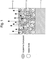
- FIG. 1 is a schematic view showing the structure of the organic EL device according to an embodiment of the present invention.
- the illustrated EL device is characterized in that a hole injection layer 3 sandwiched between an anode electrode layer (anode) 1 and an organic structure 2 including a light-emissive layer has a mixed layer of a metal oxide and an organic compound, and these two compounds react with each other to make an oxidation-reduction reaction, thereby forming a charge transfer complex which has radical cations and radical anions.
- the mixed layer can act as a hole injection layer, because radical cations (holes) in the mixed layer are moved in the direction of an cathode electrode layer (cathode) of the EL device upon voltage application to the EL device.
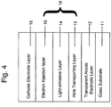
- the hole injection layer 3 includes:
- the electron-donating organic compound (a) has an ionization potential of less than 5.7 eV, because such a small ionization potential enables the organic compound to be easily changed to the radical cation state.
- the ionization potential of the organic compound is 5.7 eV or more, it becomes difficult to cause an oxidation-reduction reaction between the compound (a) and the metal oxide (b) and form a charge transfer complex of the present invention.
- the organic compound (a) is an arylamine compound
- the arylamine compound is preferably the arylamine compound represented by the following general formula (I): wherein Ar 1 , Ar 2 and Ar 3 each independently represents an aromatic hydrocarbon group which may be substituted with any substituent group.
- arylamine compound examples include, but not restricted to, the arylamine compounds disclosed in, for example, Japanese Unexamined Patent Publication (Kokai) Nos. 6-25659 , 6-203963 , 6-215874 , 7-145116 , 7-224012 , 7-157473 , 8-48656 , 7-126226 , 7-188130 , 8-40995 , 8-40996 , 8-40997 , 7-126225 , 7-101911 and 7-97355 .
- Japanese Unexamined Patent Publication (Kokai) Nos. 6-25659 , 6-203963 , 6-215874 , 7-145116 , 7-224012 , 7-157473 , 8-48656 , 7-126226 , 7-188130 , 8-40995 , 8-40996 , 8-40997 , 7-126225 , 7-101911 and 7-97355 examples include, but not restricted to, the arylamine compounds disclosed in, for example
- Suitable arylamine compounds include N,N,N',N'-tetraphenyl-4,4'-diaminophenyl, N,N'-diphenyl-N,N'-di(3-methylphenyl)-4,4'-diaminobiphenyl, 2,2-bis(4-di-p-tolylaminophenyl)propane, N,N,N',N'-tetra-p-tolyl-4,4'-diaminobiphenyl, bis(4-di-p-tolylaminophenyl)phenylmethane, N,N'-diphenyl-N,N'-di(4-methoxyphenyl)-4,4'-diaminobiphenyl, N,N,N',N'-tetraphenyl-4,4'-diaminodiphenylether, 4,4'-bis(diphenylamino)quadriphenyl,
- the arylamine compound used herein is an arylamine compound having a glass transition temperature of not lower than 90°C.
- arylamine compounds described above with reference to the formulae (II) to (V) are suitable examples of the arylamine compound having a glass transition temperature of not lower than 90°C.
- porphyrin compound including a phthalocyanine derivative can be used as an organic compound that can be mixed with the metal oxide of the present invention.
- the most suitable example of the hole injection layer to be disposed adjacent to the anode electrode layer includes a mixed layer formed from an arylamine compound (a) and (b) a metal oxide capable of forming a charge transfer complex upon an oxidation-reduction reaction of this metal oxide with the arylamine compound (a).
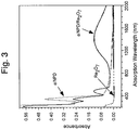
- the absorption spectrum of each of the mixed layers is not a product of the simple accumulation of the spectrum of each of the compounds constituting the mixed layer, and the absorption spectrums of each mixture exhibit a third and/or new peak in a near IR region of about 800 to 2,000nm.
- the inventors of the present invention have studied and found that the oxidation-reduction reaction generated in the mixed layer can facilitate a charge injection from the electrode in the EL devices upon the voltage application, and as a result, a driving voltage of the EL devices can be lowered.
- the layers constituting the EL device are laminated in accordance with layer formation sequence which is similar to that of conventional organic EL devices. Namely, on a glass substrate, an anode electrode layer, a hole injection layer, an organic structure including a light-emissive layer and a cathode electrode layer are laminated in this order.
- the cathode electrode layer may be formed from the metal or ITO using a layer formation method such as resistive heating vapor deposition or sputtering.
- Example 3 aluminum is deposited on the substrate to form an anode electrode layer, followed by forming the mixed layer of the present invention as a hole injection layer, and finally ITO is deposited to form a transparent cathode electrode, thereby achieving an organic EL device having a top emission structure in which light is extracted from a layered surface side (ITO side) of the EL device.
- Al aluminum
- the proposed mixed layer is used as a hole injection layer, it becomes unexpectedly possible to eliminate the above limitation concerning use of low work function metals like Al.
- the layers constituting the organic EL device can be laminated in accordance with layer formation sequence which is reverse to that of the conventional organic EL devices. Namely, on a substrate, a cathode electrode layer, an organic structure including a light-emissive layer, a hole injection layer and an anode electrode layer are laminated in this order.
- the anode electrode layer can be formed from the metal or ITO using a layer formation method such as resistive heating vapor deposition or sputtering, after formation of the hole injection layer.
- hole injection layer (mixed layer) of the present invention can act as a damage-diminishing layer during formation of the anode electrode layer, particularly when the anode electrode layer is formed as a transparent ITO layer using a sputtering process.
- the effective function as the damage-diminishing layer of the hole injection layer is evidenced in Example 5, described below.
- a transparent and electrically conducting ITO layer acting as a cathode electrode layer can be formed on the metal-doped electron injection layer by using a sputtering method which is introduced for reducing a damage of the organic layer.
- the present invention will be further described with reference to the working examples thereof. Note, however, that the present invention is not be restricted to these working examples.
- the layer formation of the organic compound, the metal oxide, the metal and the transparent ITO electrode were carried out by using the vapor deposition apparatus of Anelva Co., and the sputtering apparatus of FTS Corp.
- the control in the deposition rate of the vapor deposition material and in the thickness of the deposited layers were carried out by using a thickness monitor with a quartz oscillator, attached to the vapor deposition apparatus, "CRTM-8000" of ULVAC.
- a stylus step meter, "P10" of Tencor Co. was used.
- the characteristics of the organic EL device were evaluated with the source meter "2400" of KEITHLEY and the luminance meter “BM-8" of TOPCON.
- a DC voltage was stepwise applied at an increasing rate of 0.2 volts per 2 seconds to the EL device to determine the luminance and the electric current after lapse of one second from the completion of each increase of the voltage.
- the spectrum of the EL device was determined by using the optical multi-channel analyzer, "PMA-11" of HAMAMATSU PHOTONICS, driven at a constant electric current.
- a glass substrate 11 has coated thereon an ITO (indium-tin oxide; Nippon Sheet Glass Co., Ltd.) having a sheet resistance of about 10 ⁇ / ⁇ as a transparent anode electrode layer 12.
- ITO indium-tin oxide
- Alq tris(8-quinolinolato)
- bathocuproine (hereinafter, referred to as "BCP") represented by the following formula (VII): and alkaline metal, cesium (Cs), are co-deposited in a molar ratio of BCP : Cs of about 4 : 1 to form an electron injection layer (metal doping layer/low resistance electron-transporting layer) 15 having a thickness of about 300 ⁇ on the light-emissive layer 14.
- BCP bathocuproine
- Cs alkaline metal, cesium
- cathode electrode layer (cathode/cathode electrode) 16 having a thickness of about 1,000 ⁇ .
- the organic EL device having a square light-emissive area of 0.2 cm (length) by 0.2 cm (width) is thus obtained.
- a DC voltage was applied to between the transparent anode electrode layer (ITO) 12 and the cathode electrode layer (Al) 16, and the luminance of the green light emitted from the light-emissive layer (Alq) 14 was measured.
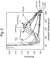
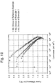
- Figures 7 to 10 The results were plotted with white circle symbols ( ⁇ ) in Figures 7 to 10 , in which Figure 7 represents a graph of current density (mA/cm 2 ) - voltage (V) characteristic curve of the EL device, Figure 8 represents a graph of luminance (cd/m 2 ) - voltage (V) characteristic curve of the EL device, Figure 9 represents a graph of current efficiency (cd/A) - current density (mA/cm 2 ) characteristic curve of the EL device and Figure 10 represents a graph of power efficiency (lm/W) - and luminance (cd/m 2 ) characteristic curve of the EL device.
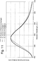
- Figures 7 to 10 each contains the results obtained in the following examples (Examples 1 and 2) in addition to the results of this reference example. Furthermore, the light emission spectrum of the EL device produced in this reference example was plotted with a thick line in Figure 11 .
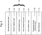
- the organic EL device having the lamination structure of Figure 5 is fabricated.
- a glass substrate 21 is coated thereon with an ITO (indium-tin oxide; Nippon Sheet Glass Co., Ltd.) having a sheet resistance of about 10 ⁇ / ⁇ as a transparent anode electrode layer (anode electrode layer) 22.
- ITO indium-tin oxide
- anode electrode layer anode electrode layer 22.
- a metal oxide, V 2 O 5 , and an organic compound having a hole transporting property, ⁇ -NPD are co-deposited at a molar ratio of V 2 O 5 : ⁇ -NPD of about 4 : 1 on the ITO-coated glass substrate 21 to form a mixed layer 27 having a thickness of about 100 ⁇ acting as a hole injection layer.
- a hole transportation layer ( ⁇ -NPD) 23 a hole transportation layer ( ⁇ -NPD) 23, a light-emissive layer (Alq) 24, an electron injection layer (metal doping layer, low resistance electron transportation layer) 25 and a cathode electrode layer (cathode) 26 are sequentially laminated as in the production of the EL device of the above-described Reference Example.
- a hole transportation layer ( ⁇ -NPD) 23 a light-emissive layer (Alq) 24, an electron injection layer (metal doping layer, low resistance electron transportation layer) 25 and a cathode electrode layer (cathode) 26 are sequentially laminated as in the production of the EL device of the above-described Reference Example.
- an organic structure 28 including a light-emissive layer is constituted from the hole transportation layer 23, the light-emissive layer 24 and the electron injection layer 25.
- the organic EL device having the lamination structure of Figure 6 is fabricated.
- a glass substrate 31 is coated thereon with an ITO (indium-tin oxide; Nippon Sheet Glass Co., Ltd.) having a sheet resistance of about 10 ⁇ / ⁇ as a transparent anode electrode layer 32.
- ITO indium-tin oxide
- a metal oxide, V 2 O 5 , and an organic compound having a hole transporting property, ⁇ -NPD are co-deposited at a molar ratio of about 4 : 1 on the ITO-coated glass substrate 31 to form a mixed layer 37 having a thickness of about 1,000 ⁇ acting as a hole injection layer of the present invention.
- a hole transportation layer ( ⁇ -NPD) 33, a light-emissive layer (Alq) 34, an electron injection layer (metal doping layer) 35 and a cathode electrode layer 36 are sequentially laminated as in the fabrication of the EL device of the above-described Reference Example.
- an organic structure 38 including a light-emissive layer is formed from the hole transportation layer 33, the light-emissive layer 34 and the electron injection layer 35.
- a DC voltage was applied to between the transparent anode electrode layer (ITO) 32 and the cathode electrode layer (Al) 36, and the luminance of the green light emitted from the light-emissive layer (Alq) 34 was measured. The results were plotted with white triangle symbols ( ⁇ ) in Figures 7 to 10 . Furthermore, the light emission spectrum of the EL device produced in this example was plotted with a thin line in Figure 11 .
- the organic EL device having the top emission structure of Figure 12 is fabricated.
- a metal oxide, V 2 O 5 , and an organic compound having a hole transporting property, ⁇ -NPD are co-deposited at a molar ratio of about 4:1 on an anode electrode layer 42 to form a mixed layer 47 having a thickness of about 100 ⁇ acting as a hole injection layer of the present invention.
- ⁇ -NPD is deposited at the deposition rate of about 2 ⁇ /sec on the hole injection layer 47 to form a hole transporting layer 43 having a thickness of about 600 ⁇ .
- Alq is deposited on the hole transportation layer 43 under the same vapor deposition conditions as in the formation of the hole transportation layer 43 to form a light-emissive layer 44 having a thickness of about 600 ⁇ .
- an electron injection layer 45 which was disclosed by the inventors of the present invention in Japanese Unexamined Patent Publication (Kokai) No. 11-233262 , (8-quinolinato) lithium complex (hereinafter, briefly referred to as "Liq") represented by the following formula (VIII): is deposited at a thickness of about 10 ⁇ , followed by depositing aluminum (Al) at the thickness of about 15 ⁇ to form an electron injection layer 15 by generating the thermal reduction reaction.
- an organic structure 48 including a light-emissive layer is formed from the hole transportation layer 43, the light-emissive layer 44 and the electron injection layer 45.
- ITO is deposited at the deposition rate of about 4 ⁇ /sec by using the sputtering method disclosed by the inventors of the present invention in Japanese Unexamined Patent Publication (Kokai) No. 2001-142627 to form a transparent cathode electrode layer 46 having a thickness of about 1,000 ⁇ .
- the EL device thus obtained has the square light-emissive area of 0.2 cm (length) by 0.2 cm (width).
- a DC voltage was applied to between the anode electrode layer (Al) 42 and the transparent cathode electrode layer (ITO) 46, and the luminance of the green light emitted from the light-emissive layer (Alq) 44 was measured.
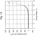
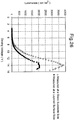
- Figure 13 represents a graph of current density (mA/cm 2 ) - voltage (V) characteristic curve of the EL device
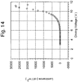
- Figure 14 represents a graph of luminance (cd/m 2 ) - voltage (V) characteristic curve of the EL device
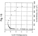
- Figure 15 represents a graph of current efficiency (cd/A) - current density (mA/cm 2 ) characteristic curve of the EL device
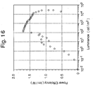
- Figure 16 represents a graph of power efficiency (lm/W) - and luminance (cd/m 2 ) characteristic curve of the EL device.
- the light emission spectrum of the EL device produced in this example was plotted in Figure 17 .
- the maximum luminance observed in the EL device of this example was above about 25,000 cd/m 2 , and also its current efficiency was comparable to the results observed in the EL devices of Reference Example and Example 1 ( Figures 15 and 16 ). Accordingly, it was found that the hole injection layer of the present invention can effectively act as such a layer, even if the anode electrode layer is formed from a lower work function metal such as Al (4.2eV) compared to ITO (5.0eV).
- a lower work function metal such as Al (4.2eV) compared to ITO (5.0eV).
- the organic EL device having the lamination structure of Figure 18 is produced.
- the EL device produced in this example has the layer structure which is in reverse to that of the conventional organic EL devices, i.e., a transparent cathode electrode layer, an organic structure including a light-emissive layer, a hole injection layer and an anode electrode layer are laminated in this order on a substrate.
- a glass substrate 51 has coated thereon an ITO (indium-tin oxide; Nippon Sheet Glass Co., Ltd.) having a sheet resistance of about 10 ⁇ / ⁇ as a transparent cathode electrode layer 56.
- BCP and Cs are co-deposited at molar ratio of about 4:1 on the ITO-coated glass substrate 51 to form a mixed layer having a thickness of about 100 ⁇ as an electron injection layer (metal doping layer) 55.
- Alq is vapor deposited on the electron injection layer 55 to form a light-emissive layer 54 having a thickness of about 600 ⁇ .
- ⁇ -NPD is deposited on the layer 54 to form a hole transporting layer 53 having a thickness of about 600 ⁇ .
- a metal oxide, V 2 O 5 , and an organic compound having a hole transporting property, ⁇ -NPD are co-deposited at a molar ratio of about 4:1 on the hole transporting layer 53 to form a hole injection layer 57 having a thickness of about 100 ⁇ .
- the EL device thus obtained has the square light-emissive area of 0.2 cm (length) by 0.2 cm (width). Note that in the EL device an organic structure 58 including a light-emissive layer is formed from the hole transporting layer 53, the light-emissive layer 54 and the electron injection layer 55.
- a DC voltage was applied to between the transparent cathode electrode layer (ITO) 56 and the anode electrode layer (Al) 52, and the luminance of the green light emitted from the light-emissive layer (Alq) 54 was measured.
- Figure 19 represents a graph of current density (mA/cm 2 ) - voltage (V) characteristic curve of the EL device
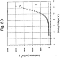
- Figure 20 represents a graph of luminance (cd/m 2 ) - voltage (V) characteristic curve of the EL device
- Figure 21 represents a graph of current efficiency (cd/A) - current density (mA/cm 2 ) characteristic curve of the EL device
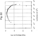
- Figure 22 represents a graph of power efficiency (lm/W) - and luminance (cd/m 2 ) characteristic curve of the EL device.
- the light emission spectrum of the EL device produced in this example was plotted in Figure 23 .
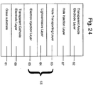
- the organic EL device having the lamination structure of Figure 24 is produced.
- the EL device produced in this example has the layer structure which is in reverse to that of the conventional organic EL devices, i.e., a transparent cathode electrode layer, an organic structure including a light-emissive layer, a hole injection layer and a transparent anode electrode layer are laminated in this order on a substrate.
- a glass substrate 61 has coated thereon an ITO (indium-tin oxide; Nippon Sheet Glass Co., Ltd.) having a sheet resistance of about 10 ⁇ / ⁇ as a transparent cathode electrode layer 66.
- BCP and Cs are co-deposited at molar ratio of about 4:1 on the ITO-coated glass substrate 61 to form a mixed layer having a thickness of about 100 ⁇ as an electron injection layer 65.
- Alq is vapor deposited on the electron injection layer 65 to form a light-emissive layer 64 having a thickness of about 600 ⁇ .
- ⁇ -NPD is deposited on the layer 64 to form a hole transporting layer 63 having a thickness of about 600 ⁇ .
- a metal oxide, V 2 O 5 , and an organic compound having a hole transporting property, ⁇ -NPD are co-deposited at a molar ratio of about 4:1 on the hole transporting layer 63 to form a hole injection layer 57 having a thickness of about 100 ⁇ .
- an organic structure 68 including a light-emissive layer is constituted from the hole transporting layer 63, the light-emissive layer 64 and the electron injection layer 65. Then, ITO is deposited at the deposition rate of about 4 ⁇ /sec by using the sputtering method to form a transparent anode electrode layer (anode layer) 62 having a thickness of about 1,000 ⁇ .
- the EL device thus obtained has the square light-emissive area of 0.2 cm (length) by 0.2 cm (width).
- a DC voltage was applied to between the transparent cathode electrode layer (ITO) 66 and the transparent anode electrode layer (ITO) 62, and the luminance of the green light emitted from the light-emissive layer (Alq) 64 was measured.
- Figure 25 represents a graph of current density (mA/cm 2 ) - voltage (V) characteristic curve of the EL device
- Figure 26 represents a graph of luminance (cd/m 2 ) - voltage (V) characteristic curve of the EL device
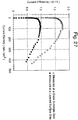
- Figure 27 represents a graph of current efficiency (cd/A) - current density (mA/cm 2 ) characteristic curve of the EL device
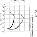
- Figure 28 represents a graph of power efficiency (lm/W) - and luminance (cd/m 2 ) characteristic curve of the EL device.
- the results measured at a side of the glass substrate (substrate) of the EL device were plotted with white circle symbols ( ⁇ ), and the results measured at a side of the layered surface of the EL device were plotted with black circle symbols ( ⁇ ).
- the emission spectrums measured at a side of the glass substrate (substrate) of the EL device were indicated with a solid line, and the emission spectrums measured at a side of the layered surface of the EL device were indicated with a dotted line.
- the organic EL device produced in this example is a transparent light-emissive device in which the light emission can be observed on both of the glass substrate side and the layered surface side (side of the transparent anode electrode layer) of the EL device.
- the emission spectrums of the light emitted from these sides of the EL device are different from each other because of the optical interference effect described above.
- the layers constituting the EL device are laminated in the reverse order to the conventional EL devices, and a hole injection layer is formed before the final formation of the anode electrode layer. Accordingly, an organic structure 68 including a light-emissive layer is protected with the hole injection layer 67 from the high energy particles induced process such as the ITO-sputtering process used in the formation of the transparent anode electrode layer 62, and thus any damage caused in the organic structure 68 due to such process can be reduced. Therefore, it was found that the hole injection layer 67 can effectively act as a damage-diminishing layer.
- the EL device may have the layer structure that two or more light-emissive units (a layered portion sandwiched between the cathode electrode layer and the anode electrode layer; when the EL device includes a layer structure of, for example, "(anode) / hole injection layer / hole transportation layer / light-emissive layer / electron injection layer / (cathode)", the "hole injection layer / hole transportation layer / light-emissive layer / electron injection layer" corresponds to the "light-emissive unit”) are partitioned with a charge-generation layer.
- the charge-generation layer can act as a hole-generating layer and an electron-generating layer during application of voltage, and as a result, the light-emissive units can simultaneously emit light as in operation of two or more organic EL devices connected in series.
- the charge-generation layer can act as a hole injection layer with regard to the light-emissive unit adjacent and disposed on a cathode electrode layer side thereof, and also it can act as an electron injection layer with regard to the light-emissive unit adjacent and disposed on an anode electrode layer side thereof.
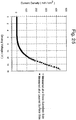
- the resistivity ( ⁇ cm) of the hole injection layer according to the present invention is measured for the reference.
- the measurement is carried out with two different methods depending on the values (range) of the resistivity of the test samples.
- the first measuring method is a method suitable for the test samples having a relatively large resistivity, and the measurement process is carried out by sandwiching a vapor deposition layer of the test sample with electrodes (the resistivity evaluation device having a sandwich structure shown in Figures 30 and 31 ).
- the resistivity evaluation device used in this test example is produced by depositing a test sample (a material to be measured) 103 at a desired thickness on an ITO electrode 101 or, if necessary, an aluminum electrode having a width of about 2 mm, followed by finally depositing an aluminum electrode 102 (having a width of about 2 mm as in the above aluminum electrode) in such a manner that the aluminum electrode 102 is crossed with the ITO electrode 101.
- the second measuring method is a method suitable for the test samples having a relatively small resistivity, and the measurement process is carried out by using a resistivity evaluation device having a co-planar arrangement structure. Namely, as shown in Figures 32 and 33 , a substrate 200 having previously deposited as layers on the same plane surface thereof electrodes which are used as an anode electrode layer 201 and a cathode electrode layer 202 are prepared. The anode electrode layer 201 and the cathode electrode layer 202 are disposed at a certain distance of L (cm).
- a test sample material is deposited, through a metal mask of defining a deposition area and having an opening with the certain width W (cm), on the substrate 200 to form a deposited layer 203 of the test sample having a predetermined thickness t (cm).
- an electric field E(V/cm) of the test sample is calculated by dividing an applied voltage (V) with a distance L (cm) between the electrodes, and a current density (A/cm 2 ) is calculated by dividing a measured current value (A) by a cross-sectional area of the current flowing region [in this example, W x t (cm 2 )].
- the resistivity ( ⁇ cm) of the test sample can be calculated from the equation described above with regard to the first measuring method (sandwich method).
- the resistivity of each of ITO, the co-deposition layer of V 2 O 5 and ⁇ -NPD and the co-deposition layer of V 2 O 5 and 2-TNATA is measured using the measuring device having a co-planar arrangement structure.
- the resistivity of each of the co-deposition layer of Cs and BCP, ⁇ -NPD and Alq 3 is measured using the measuring device having a sandwich structure.
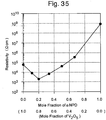
- the measurement of the resistivity is carried out after forming the co-deposition layer of V 2 O 5 and ⁇ -NPD, i.e., the hole injection layer of the present invention, at a relatively thin thickness of 50 ⁇ in a portion adjacent to each of the electrodes, followed by sandwiching a 1,000 ⁇ -thick ⁇ -NPD layer with the electrodes. Furthermore, the resistivity of V 2 O 5 is measured using both of the co-planar arrangement method and the sandwich method to confirm that substantially same resistivities can be obtained regardless of the measuring methods used.
- the resistivities of the hole injection layer including V 2 O 5 are within the range of not less than 1.0 x 10 2 ⁇ cm and less than 1.0 x 10 10 ⁇ cm.
- the hole injection layer As is shown in Figure 35 , the hole injection layer according the above-described embodiments has a mixed layer of the metal oxide and the organic compound, and because of mixing of these two compounds, the hole injection layer shows a low resistivity which cannot be obtained with a sole use of each of the compounds. Furthermore, this fact indicates that the hole injection layer includes an oxidation-reduction reaction as a result of electron transfer therein, and thus basically evidences that the hole injection layer is effective in lowering a driving voltage and increasing an efficiency in the EL devices.
- a thickness of the hole injection layer is not specifically restricted to, but it is desirable that the thickness is 5 ⁇ or more.
- its thickness has no upper limit because the arylamine compound is contained in a state of radical cations which can act as an internal charge in the hole injection layer even when no electric field is applied to the device.
- the hole injection layer does not cause an increase of the voltage of the EL device, and therefore, when a distance between the electrodes is extended to be larger than that of conventional organic EL devices, the hole injection layer is useful for largely reducing a risk of the short-circuit in EL devices. Accordingly, the organic EL devices of the present invention can be operated at a low voltage as in the conventional organic EL devices, even if a total thickness of the layers between the electrodes is increased to not less than about 2.000 ⁇ .
- a driving voltage of the organic EL devices can be reduced by lowering an energy barrier during hole injection from the anode electrode layer to the organic compound layer, and at the same time, a risk of the electrical short-circuit between the cathode electrode layer and the anode electrode layer can be considerably diminished by controlling the thickness of the hole injection layer. Furthermore, it becomes possible for the hole injection layer, which is a mixed layer of the metal oxide compound and the organic compound, to act as a buffer layer for reducing damages due to high energy particles caused in the formation of the electrodes using the sputtering method.
- the mixed layer is used as a hole injection layer in adjacent to the anode electrode layer, since the organic molecules used in the formation of the mixed layer such as arylamines have been already in the state of radical cations, it becomes possible to inject holes into the organic structure including a light-emissive layer without suffering from an energy barrier during application of the voltage, regardless of the types of the anode electrode material used.
Landscapes
- Physics & Mathematics (AREA)
- Optics & Photonics (AREA)
- Chemical & Material Sciences (AREA)
- Engineering & Computer Science (AREA)
- Materials Engineering (AREA)
- Organic Chemistry (AREA)
- Electroluminescent Light Sources (AREA)
Claims (16)
- Verfahren zum Herstellen einer organischen Elektrolumineszenzvorrichtung durch Vorsehen einer Schichtstruktur, umfassend:eine Anodenschicht (1);eine Kathodenschicht, die entgegengesetzt zu der Anodenschicht (1) angeordnet ist; undSchichten, die zwischen der Anodenschicht (1) und der Kathodenschicht vorgesehen sind, wobei die genannten Schichten eine Löcherinjektionsschicht (3), die an die Anodenschicht (1) angrenzend vorgesehen ist, und eine organische Struktur (2) beinhalten, die mindestens eine lichtemittierende Schicht oder mindestens eine lichtemittierende Einheit mit mindestens einer lichtemittierenden Schicht enthält;wobei mindestens eine der Anodenschicht (1) und der Kathodenschicht transparent ist;dadurch gekennzeichnet, dassdie Löcherinjektionsschicht (3) eine gemischte Schicht aus Metalloxid und einer organischen Verbindung enthält;wobei die gemischte Schicht durch eine gemischte Ablagerung des Metalloxids und der organischen Verbindung gebildet wird; undwobei das Metalloxid nach einem Widerstandsheiz-Aufdampfverfahren oder einem Elektronenstrahl-Aufdampfverfahren oder einem Laserstrahl-Aufdampfverfahren aufgedampft wird.
- Verfahren nach Anspruch 1, bei dem die organische Verbindung in der gemischten Schicht eine lonisierungspotential von weniger als 5,7 eV hat und eine Löchertransporteigenschaft aufweist,
wobei die gemischte Schicht einen Ladungstransferkomplex mit einem radikalen Kation der organischen Verbindung und einem radikalen Anion des Metalloxids enthält, wobei der Ladungstransferkomplex mittels einer Oxidationsreduktionsreaktion zwischen dem Metalloxid und der organischen Verbindung hergestellt wird; und
wobei das radikale Kation in dem Ladungstransferkomplex während des Anlegens der Spannung an die EL-Vorrichtung in Richtung der Kathodenschicht bewegt wird, wodurch Löcher in die lichtemittierende Schicht injiziert werden. - Verfahren nach Anspruch 2, bei dem die organische Verbindung eine Arylamin-Verbindung enthält, die durch die allgemeine Formel (I) dargestellt ist:

- Verfahren nach Anspruch 2, wobei die organische Verbindung eine Porphyrin-Verbindung ist, die ein Phtalocyanin-Derivat enthält.
- Verfahren nach Anspruch 3, bei dem die organische Verbindung eine Arylamin-Verbindung ist, die eine Glasübergangstemperatur von nicht weniger als 90°C hat.
- Verfahren nach Anspruch 5, bei dem die als organische Verbindung verwendete Arylamin-Verbindung eine der Substanzen α-NPD, 2-TNATA, Spiro-TAD und Spiro-NPB enthält.
- Verfahren nach einem der Ansprüche 1 bis 6, bei dem das Metalloxid eine der Substanzen V2O5 und Re2O7 enthält.
- Verfahren nach einem der Ansprüche 1 bis 7, bei dem die EL-Vorrichtung ein Substrat enthält, auf das die Anodenschicht (1), die Löcherinjektionsschicht (3) und eine organische Struktur, welche die lichtemittierende Schicht und die Kathodenschicht enthält, in dieser Reihenfolge geschichtet werden.
- Verfahren nach einem der Ansprüche 1 bis 7, bei dem die EL-Vorrichtung ein Substrat enthält, auf das die Kathodenschicht, eine organische Struktur, welche die lichtemittierende Schicht enthält, die Löcherinjektionsschicht (3) und die Anodenschicht (1) in dieser Reihenfolge geschichtet werden.
- Verfahren nach Anspruch 8, bei dem ein Mischungsverhältnis des Metalloxids und der organischen Verbindung in der Löcherinjektionsschicht (3) von der Anodenschicht (1) zu der die lichtemittierenden Schicht enthaltenden organischen Struktur kontinuierlich variiert wird.
- Verfahren nach Anspruch 9, bei dem ein Mischungsverhältnis des Metalloxids und der organischen Verbindung in der Löcherinjektionsschicht (3) von der Anodenschicht (1) zu der die lichtemittierende Schicht enthaltenden organischen Struktur kontinuierlich variiert wird.
- Verfahren nach Anspruch 8, bei dem ein Mischungsverhältnis des Metalloxids und der organischen Verbindung in der Löcherinjektionsschicht (3) ausgehend von der Anodenschicht (1) bis zu der die lichtemittierenden Schicht enthaltenden organischen Struktur diskontinuierlich variiert wird.
- Verfahren nach Anspruch 9, bei dem ein Mischungsverhältnis des Metalloxids und der organischen Verbindung in der Löcherinjektionsschicht (3) von der Anodenschicht (1) zu der die lichtemittierende Schicht enthaltenden organischen Struktur diskontinuierlich variiert wird.
- Verfahren nach Anspruch 9, bei dem die Anodenschicht nach einem Sputter-Verfahren ausgebildet wird.
- Verfahren nach Anspruch 14, bei dem eine in dem Sputter-Verfahren verwendete Sputter-Einrichtung ein Sputter-System mit zugewandten Targets umfasst, das ein Paar einander gegenüberliegender, in einem vorbestimmten Abstand voneinander vorgesehener Targets, eine Reflexionselektrode, die imstande ist, Elektronen auf einen vorderen Randbereich des jeweiligen Targets zu reflektieren, und ein Magnetfeld-Erzeugungsmedium enthält, das imstande ist, ein paralleles Magnetfeld in der Nähe des Randteils des jeweiligen Targets zu erzeugen, wobei das Magnetfeld einen zu dem Randteil des Targets parallelen Abschnitt hat.
- Verfahren nach einem der Ansprüche 1 bis 15, bei dem die Löcherinjektionsschicht (3), die eine gemischte Schicht aus dem Metalloxid der organischen Verbindung ist, einen spezifischen elektrischen Widerstand von nicht weniger als 1,0 x 10² Ω cm und weniger als 1,0 x 10¹⁰ Ω cm hat.
Applications Claiming Priority (2)
| Application Number | Priority Date | Filing Date | Title |
|---|---|---|---|
| JP2003358402A JP4476594B2 (ja) | 2003-10-17 | 2003-10-17 | 有機エレクトロルミネッセント素子 |
| JP2003358402 | 2003-10-17 |
Publications (3)
| Publication Number | Publication Date |
|---|---|
| EP1524706A2 EP1524706A2 (de) | 2005-04-20 |
| EP1524706A3 EP1524706A3 (de) | 2006-05-10 |
| EP1524706B1 true EP1524706B1 (de) | 2017-05-03 |
Family
ID=34373644
Family Applications (1)
| Application Number | Title | Priority Date | Filing Date |
|---|---|---|---|
| EP04024610.0A Active EP1524706B1 (de) | 2003-10-17 | 2004-10-15 | Methode zum Herstellen einer organischen elektrolumineszenten Vorrichtung |
Country Status (7)
| Country | Link |
|---|---|
| US (1) | US8558451B2 (de) |
| EP (1) | EP1524706B1 (de) |
| JP (1) | JP4476594B2 (de) |
| KR (1) | KR100894306B1 (de) |
| CN (1) | CN100466331C (de) |
| ES (1) | ES2636486T3 (de) |
| TW (1) | TWI367048B (de) |
Families Citing this family (127)
| Publication number | Priority date | Publication date | Assignee | Title |
|---|---|---|---|---|
| JPWO2005002010A1 (ja) * | 2003-06-27 | 2006-08-10 | 株式会社半導体エネルギー研究所 | 有機レーザー装置 |
| US20050008052A1 (en) * | 2003-07-01 | 2005-01-13 | Ryoji Nomura | Light-emitting device |
| WO2005031798A2 (en) | 2003-09-26 | 2005-04-07 | Semiconductor Energy Laboratory Co., Ltd. | Light-emitting device and method for manufacturing the same |
| US7605534B2 (en) * | 2003-12-02 | 2009-10-20 | Semiconductor Energy Laboratory Co., Ltd. | Light-emitting element having metal oxide and light-emitting device using the same |
| WO2005064995A1 (en) | 2003-12-26 | 2005-07-14 | Semiconductor Energy Laboratory Co., Ltd. | Light-emitting element |
| CN100531497C (zh) * | 2004-05-21 | 2009-08-19 | 株式会社半导体能源研究所 | 发光元件和发光设备 |
| JP4925569B2 (ja) * | 2004-07-08 | 2012-04-25 | ローム株式会社 | 有機エレクトロルミネッセント素子 |
| JP2006295104A (ja) | 2004-07-23 | 2006-10-26 | Semiconductor Energy Lab Co Ltd | 発光素子およびそれを用いた発光装置 |
| EP1624502B1 (de) * | 2004-08-04 | 2015-11-18 | Semiconductor Energy Laboratory Co., Ltd. | Lichtemittierende Vorrichtung, Anzeigevorrichtung und elektronisches Gerät |
| CN101841002B (zh) | 2004-09-24 | 2011-11-16 | 株式会社半导体能源研究所 | 发光器件 |
| WO2006035958A1 (en) * | 2004-09-30 | 2006-04-06 | Semiconductor Energy Laboratory Co., Ltd. | Light emitting element |
| US20070262693A1 (en) * | 2004-10-29 | 2007-11-15 | Satoshi Seo | Composite Material, Light-Emitting Element, Light-Emitting Device and Manufacturing Method Thereof |
| US7683532B2 (en) | 2004-11-02 | 2010-03-23 | Semiconductor Energy Laboratory Co., Ltd. | Semiconductor device and light emitting device |
| WO2006059736A1 (en) * | 2004-11-30 | 2006-06-08 | Semiconductor Energy Laboratory Co., Ltd. | Light emitting element, light emitting device, and electronic device |
| KR101326286B1 (ko) * | 2004-11-30 | 2013-11-11 | 가부시키가이샤 한도오따이 에네루기 켄큐쇼 | 발광 소자 및 발광 장치 |
| CN101116197B (zh) * | 2004-12-06 | 2010-05-12 | 株式会社半导体能源研究所 | 包含有机化合物和无机化合物的复合材料、使用所述复合化合物的发光元件和发光器件以及所述发光元件的制造方法 |
| JP4789598B2 (ja) * | 2004-12-06 | 2011-10-12 | 株式会社半導体エネルギー研究所 | 発光素子及び電子機器 |
| JP2006164708A (ja) | 2004-12-06 | 2006-06-22 | Semiconductor Energy Lab Co Ltd | 電子機器および発光装置 |
| US7989694B2 (en) * | 2004-12-06 | 2011-08-02 | Semiconductor Energy Laboratory Co., Ltd. | Photoelectric conversion element, solar battery, and photo sensor |
| US8569742B2 (en) * | 2004-12-06 | 2013-10-29 | Semiconductor Energy Laboratory Co., Ltd. | Organic field-effect transistor and semiconductor device including the same |
| JP2006190995A (ja) * | 2004-12-06 | 2006-07-20 | Semiconductor Energy Lab Co Ltd | 有機化合物と無機化合物とを含む複合材料、前記複合材料を用いた発光素子および発光装置、並びに前記発光素子の作製方法 |
| WO2006062218A1 (en) * | 2004-12-06 | 2006-06-15 | Semiconductor Energy Laboratory Co., Ltd. | Light-emitting element and light-emitting device using the same |
| US7919772B2 (en) * | 2004-12-14 | 2011-04-05 | Semiconductor Energy Laboratory Co., Ltd. | Semiconductor device and manufacturing method thereof |
| US8217569B2 (en) | 2004-12-28 | 2012-07-10 | Semiconductor Energy Laboratory Co., Ltd. | Low drive voltage light emitting element |
| WO2006080553A1 (en) * | 2005-01-31 | 2006-08-03 | Semiconductor Energy Laboratory Co., Ltd. | Hole-injecting material, material for light-emitting element, light-emitting element, organic compound, monomer, and monomer mixture |
| US8426034B2 (en) | 2005-02-08 | 2013-04-23 | Semiconductor Energy Laboratory Co., Ltd. | Light-emitting element, light-emitting device, and electronic appliance |
| JP5159042B2 (ja) * | 2005-02-08 | 2013-03-06 | 株式会社半導体エネルギー研究所 | 発光素子、発光装置及び電子機器 |
| US9530968B2 (en) * | 2005-02-15 | 2016-12-27 | Semiconductor Energy Laboratory Co., Ltd. | Light emitting element and light emitting device |
| WO2006093171A1 (en) * | 2005-02-28 | 2006-09-08 | Semiconductor Energy Laboratory Co., Ltd. | Composite material, light emitting element, light emitting device and electronic appliance using the composite material |
| JP5707013B2 (ja) * | 2005-02-28 | 2015-04-22 | 株式会社半導体エネルギー研究所 | 複合材料、並びに前記複合材料を用いた発光素子、発光装置及び電気機器 |
| US7626198B2 (en) * | 2005-03-22 | 2009-12-01 | Semiconductor Energy Laboratory Co., Ltd. | Nonlinear element, element substrate including the nonlinear element, and display device |
| US7649197B2 (en) | 2005-03-23 | 2010-01-19 | Semiconductor Energy Laboratory Co., Ltd. | Composite material, and light emitting element and light emitting device using the composite material |
| WO2006101016A1 (en) | 2005-03-23 | 2006-09-28 | Semiconductor Energy Laboratory Co., Ltd. | Composite material, light emitting element and light emitting device |
| US7977865B2 (en) * | 2005-03-23 | 2011-07-12 | Semiconductor Energy Laboratory Co., Ltd. | Composite material, material for light-emitting element, light-emitting element, light-emitting device and electronic device |
| JP5072243B2 (ja) * | 2005-03-25 | 2012-11-14 | 株式会社半導体エネルギー研究所 | 発光装置 |
| US7851989B2 (en) | 2005-03-25 | 2010-12-14 | Semiconductor Energy Laboratory Co., Ltd. | Light emitting device |
| US7777232B2 (en) * | 2005-04-11 | 2010-08-17 | Semiconductor Energy Laboratory Co., Ltd. | Display device and electronic device using the same |
| US8125144B2 (en) * | 2005-04-11 | 2012-02-28 | Semiconductor Energy Laboratory Co., Ltd. | Light-emitting element, light-emitting device, and vapor deposition apparatus |
| JP5314834B2 (ja) * | 2005-04-21 | 2013-10-16 | 株式会社半導体エネルギー研究所 | 発光素子、発光装置、照明装置および電子機器 |
| US20090026922A1 (en) * | 2005-04-21 | 2009-01-29 | Semiconductor Energy Laboratory Co., Ltd. | Light emitting element, light emitting device, and electronic device |
| KR101182263B1 (ko) * | 2005-04-22 | 2012-09-17 | 가부시키가이샤 한도오따이 에네루기 켄큐쇼 | 유기 트랜지스터용 전극, 유기 트랜지스터, 및 반도체장치 |
| US7745019B2 (en) * | 2005-04-28 | 2010-06-29 | Semiconductor Energy Laboratory Co., Ltd. | Light emitting element and light emitting device and method of manufacturing light emitting element |
| US20060250078A1 (en) * | 2005-05-09 | 2006-11-09 | City University Of Hong Kong | Organic electroluminescent devices incorporating UV-illuminated fluorocarbon layers |
| EP1724852A3 (de) | 2005-05-20 | 2010-01-27 | Semiconductor Energy Laboratory Co., Ltd. | Lichtemittierendes Bauelement, lichtemittierende Vorrichtung, und elektronische Vorrichtung |
| JP4596976B2 (ja) * | 2005-05-20 | 2010-12-15 | 株式会社 日立ディスプレイズ | 有機発光表示装置 |
| JP2006324537A (ja) * | 2005-05-20 | 2006-11-30 | Hitachi Displays Ltd | 表示装置 |
| US7687986B2 (en) | 2005-05-27 | 2010-03-30 | Fujifilm Corporation | Organic EL device having hole-injection layer doped with metallic oxide |
| JP5116992B2 (ja) * | 2005-05-27 | 2013-01-09 | 富士フイルム株式会社 | 有機el素子 |
| US8334057B2 (en) | 2005-06-08 | 2012-12-18 | Semiconductor Energy Laboratory Co., Ltd. | Light-emitting element, light-emitting device, and electronic device |
| JP2006344774A (ja) * | 2005-06-09 | 2006-12-21 | Rohm Co Ltd | 有機el素子、これを用いた有機el表示装置、および有機el素子の製造方法 |
| US8269227B2 (en) | 2005-06-09 | 2012-09-18 | Semiconductor Energy Laboratory Co., Ltd. | Light emitting device and electronic device |
| JP2007019487A (ja) * | 2005-06-09 | 2007-01-25 | Semiconductor Energy Lab Co Ltd | 発光装置及び電子機器 |
| US8395313B2 (en) | 2005-06-10 | 2013-03-12 | Thomson Licensing | Light-emitting organic diode comprising not more than two layers of different organic materials |
| US8017252B2 (en) | 2005-06-22 | 2011-09-13 | Semiconductor Energy Laboratory Co., Ltd. | Light emitting device and electronic appliance using the same |
| JP5072271B2 (ja) * | 2005-06-22 | 2012-11-14 | 株式会社半導体エネルギー研究所 | 発光装置、及びそれを用いた電子機器 |
| US8729795B2 (en) * | 2005-06-30 | 2014-05-20 | Semiconductor Energy Laboratory Co., Ltd. | Light emitting device and electronic device |
| JP4890117B2 (ja) * | 2005-06-30 | 2012-03-07 | 株式会社半導体エネルギー研究所 | 発光装置及びその作製方法 |
| US7745989B2 (en) | 2005-06-30 | 2010-06-29 | Semiconductor Energy Laboratory Co., Ltd | Light emitting element, light emitting device, and electronic apparatus |
| JP5132092B2 (ja) * | 2005-06-30 | 2013-01-30 | 株式会社半導体エネルギー研究所 | 発光素子の製造方法 |
| US8288180B2 (en) | 2005-07-04 | 2012-10-16 | Semiconductor Energy Laboratory Co., Ltd. | Method for manufacturing light emitting device |
| US8415878B2 (en) * | 2005-07-06 | 2013-04-09 | Semiconductor Energy Laboratory Co., Ltd. | Light-emitting element, light-emitting device, and electronic device |
| US8659008B2 (en) | 2005-07-08 | 2014-02-25 | Semiconductor Energy Laboratory Co., Ltd. | Composite material and light emitting element, light emitting device, and electronic device using the composite material |
| JP4954623B2 (ja) * | 2005-07-08 | 2012-06-20 | 株式会社半導体エネルギー研究所 | 発光装置 |
| WO2007013478A1 (en) | 2005-07-25 | 2007-02-01 | Semiconductor Energy Laboratory Co., Ltd. | Light-emitting element, light-emitting device, and electronic appliance |
| KR101288588B1 (ko) * | 2005-08-12 | 2013-07-22 | 가부시키가이샤 한도오따이 에네루기 켄큐쇼 | 아릴아민 화합물 및 그의 합성 방법 |
| WO2007032258A1 (en) * | 2005-09-12 | 2007-03-22 | Semiconductor Energy Laboratory Co., Ltd. | Quinoxaline derivative, and light emitting element, light emitting device, and electronic appliance using the same |
| US20070108894A1 (en) * | 2005-11-17 | 2007-05-17 | Idemitsu Kosan Co., Ltd. | Organic electroluminescent device |
| JP5078329B2 (ja) * | 2005-11-30 | 2012-11-21 | 株式会社半導体エネルギー研究所 | 発光素子、発光装置並びに電子機器 |
| JP2007227907A (ja) * | 2006-01-26 | 2007-09-06 | Semiconductor Energy Lab Co Ltd | 有機電界効果トランジスタ及び半導体装置 |
| KR101381365B1 (ko) | 2006-01-26 | 2014-04-04 | 가부시키가이샤 한도오따이 에네루기 켄큐쇼 | 유기 전계효과 트랜지스터 및 반도체장치 |
| EP1821579A3 (de) * | 2006-02-17 | 2008-04-02 | Semiconductor Energy Laboratory Co., Ltd. | Lichtemittierendes Element, lichtemittierende Vorrichtung und elektronisches Gerät |
| US20070194321A1 (en) * | 2006-02-17 | 2007-08-23 | Semiconductor Energy Laboratory Co., Ltd. | Light emitting element, light emitting device, and electronic device |
| TWI277367B (en) * | 2006-03-03 | 2007-03-21 | Au Optronics Corp | Hole injection structure of organic electroluminescence device and method for manufacturing the same |
| JP4975766B2 (ja) * | 2006-03-07 | 2012-07-11 | エルジー・ケム・リミテッド | 有機発光素子およびその製造方法 |
| KR100823443B1 (ko) | 2006-03-14 | 2008-04-18 | 주식회사 엘지화학 | 고효율 유기발광소자 및 이의 제조 방법 |
| US20070215889A1 (en) * | 2006-03-20 | 2007-09-20 | Semiconductor Energy Laboratory Co., Ltd. | Aromatic amine compound, and light-emitting element, light-emitting device, and electronic appliance using the aromatic amine compound |
| US9112170B2 (en) | 2006-03-21 | 2015-08-18 | Semiconductor Energy Laboratory Co., Ltd. | Light-emitting element, light-emitting device, and electronic device |
| JP2008034367A (ja) * | 2006-07-04 | 2008-02-14 | Semiconductor Energy Lab Co Ltd | 表示装置 |
| US8974918B2 (en) * | 2006-07-04 | 2015-03-10 | Semiconductor Energy Laboratory Co., Ltd. | Display device and electronic device |
| JP2008112904A (ja) * | 2006-10-31 | 2008-05-15 | Idemitsu Kosan Co Ltd | 有機エレクトロルミネッセンス素子 |
| US20080111131A1 (en) * | 2006-11-10 | 2008-05-15 | Nam-Choul Yang | Organic thin film transistor, method of fabricating the same, and display device including the same |
| TW200824497A (en) * | 2006-11-21 | 2008-06-01 | Au Optronics Corp | Organic electro-luminescent device |
| CN1976087B (zh) * | 2006-12-04 | 2010-09-08 | 友达光电股份有限公司 | 有机电激发光装置 |
| WO2008069259A1 (en) | 2006-12-05 | 2008-06-12 | Semiconductor Energy Laboratory Co., Ltd. | Film formation apparatus, film formation method, manufacturing apparatus, and method for manufacturing light-emitting device |
| WO2008075615A1 (en) | 2006-12-21 | 2008-06-26 | Semiconductor Energy Laboratory Co., Ltd. | Light-emitting element and light-emitting device |
| WO2008108254A1 (en) * | 2007-03-07 | 2008-09-12 | Semiconductor Energy Laboratory Co., Ltd. | Light-emitting element and light-emitting device |
| CN101271869B (zh) * | 2007-03-22 | 2015-11-25 | 株式会社半导体能源研究所 | 发光器件的制造方法 |
| JP2008251626A (ja) * | 2007-03-29 | 2008-10-16 | Kyocera Corp | 有機el素子および有機el素子の製造方法、並びに有機elディスプレイ |
| PL1986473T3 (pl) * | 2007-04-03 | 2017-07-31 | Tsinghua University | Organiczne urządzenie elektroluminescencyjne |
| US7875881B2 (en) * | 2007-04-03 | 2011-01-25 | Semiconductor Energy Laboratory Co., Ltd. | Memory device and semiconductor device |
| KR101482760B1 (ko) * | 2007-06-14 | 2015-01-15 | 가부시키가이샤 한도오따이 에네루기 켄큐쇼 | 발광장치 및 전자기기, 및 발광장치의 제조 방법 |
| US8093806B2 (en) | 2007-06-20 | 2012-01-10 | Semiconductor Energy Laboratory Co., Ltd. | Light-emitting device, method for manufacturing the same, and electronic apparatus |
| JP5208591B2 (ja) | 2007-06-28 | 2013-06-12 | 株式会社半導体エネルギー研究所 | 発光装置、及び照明装置 |
| KR102340209B1 (ko) * | 2007-12-03 | 2021-12-17 | 가부시키가이샤 한도오따이 에네루기 켄큐쇼 | 카바졸 유도체, 및 카바졸 유도체를 사용하는 발광 소자, 발광 장치 및 전자 기기 |
| EP2075850A3 (de) * | 2007-12-28 | 2011-08-24 | Semiconductor Energy Laboratory Co, Ltd. | Photoelektrische Umwandlungsvorrichtung und Verfahren zu ihrer Herstellung |
| JP5603254B2 (ja) * | 2008-01-23 | 2014-10-08 | エルジー・ケム・リミテッド | 有機発光素子およびその製作方法 |
| JP2010153365A (ja) | 2008-11-19 | 2010-07-08 | Semiconductor Energy Lab Co Ltd | 発光素子、発光装置、電子機器及び照明装置 |
| JP5717944B2 (ja) * | 2008-11-21 | 2015-05-13 | ユー・ディー・シー アイルランド リミテッド | 有機電界発光素子及びその製造方法 |
| KR101707430B1 (ko) * | 2009-05-29 | 2017-02-16 | 가부시키가이샤 한도오따이 에네루기 켄큐쇼 | 발광 소자, 발광 장치, 조명 장치 및 전자기기 |
| US9741955B2 (en) | 2009-05-29 | 2017-08-22 | Semiconductor Energy Laboratory Co., Ltd. | Light-emitting element, light-emitting device, and method for manufacturing the same |
| CN102484923B (zh) * | 2009-09-04 | 2016-05-04 | 株式会社半导体能源研究所 | 发光元件、发光装置及其制造方法 |
| DE102009047883A1 (de) * | 2009-09-30 | 2011-03-31 | Osram Opto Semiconductors Gmbh | Optoelektronisches organisches Bauelement und Verfahren zu dessen Herstellung |
| US8404500B2 (en) | 2009-11-02 | 2013-03-26 | Semiconductor Energy Laboratory Co., Ltd. | Method for manufacturing light-emitting element, light-emitting element, light-emitting device, lighting device, and electronic appliance |
| JP2011139044A (ja) | 2009-12-01 | 2011-07-14 | Semiconductor Energy Lab Co Ltd | 発光素子、発光装置、電子機器、および照明装置 |
| KR101912675B1 (ko) | 2010-10-04 | 2018-10-29 | 가부시키가이샤 한도오따이 에네루기 켄큐쇼 | 복합 재료, 발광 소자, 발광 장치, 전자 기기, 및 조명 장치 |
| JP2012182443A (ja) | 2011-02-11 | 2012-09-20 | Semiconductor Energy Lab Co Ltd | 発光素子及び発光装置 |
| JP5969216B2 (ja) | 2011-02-11 | 2016-08-17 | 株式会社半導体エネルギー研究所 | 発光素子、表示装置、照明装置、及びこれらの作製方法 |
| KR101894898B1 (ko) * | 2011-02-11 | 2018-09-04 | 가부시키가이샤 한도오따이 에네루기 켄큐쇼 | 발광 장치 및 발광 장치를 사용한 전자 기기 |
| US20120234392A1 (en) * | 2011-03-17 | 2012-09-20 | Semiconductor Energy Laboratory Co., Ltd. | Photoelectric conversion device |
| EP2503618B1 (de) | 2011-03-23 | 2014-01-01 | Semiconductor Energy Laboratory Co., Ltd. | Verbundmaterial, lichtemittierendes Element, lichtemittierende Vorrichtung, elektronische Vorrichtung und Beleuchtungsvorrichtung |
| KR101960759B1 (ko) * | 2011-04-08 | 2019-03-21 | 가부시키가이샤 한도오따이 에네루기 켄큐쇼 | 발광 장치, 전자 기기, 및 조명 장치 |
| JP6023461B2 (ja) | 2011-05-13 | 2016-11-09 | 株式会社半導体エネルギー研究所 | 発光素子、発光装置 |
| US9419239B2 (en) * | 2011-07-08 | 2016-08-16 | Semiconductor Energy Laboratory Co., Ltd. | Composite material, light-emitting element, light-emitting device, electronic device, lighting device, and organic compound |
| US9159939B2 (en) | 2011-07-21 | 2015-10-13 | Semiconductor Energy Laboratory Co., Ltd. | Photoelectric conversion device |
| JP2013058562A (ja) | 2011-09-07 | 2013-03-28 | Semiconductor Energy Lab Co Ltd | 光電変換装置 |
| CN103050641B (zh) * | 2011-10-14 | 2016-03-02 | 乐金显示有限公司 | 有机发光器件和使用该器件的显示板 |
| DE102012200084B4 (de) | 2012-01-04 | 2021-05-12 | Pictiva Displays International Limited | Strahlungsemittierendes organisches bauteil |
| JP5892924B2 (ja) * | 2012-12-28 | 2016-03-23 | エルジー ディスプレイ カンパニー リミテッド | 有機el素子および有機el素子の製造方法、並びに有機elディスプレイ |
| CN104051632A (zh) * | 2013-03-11 | 2014-09-17 | 海洋王照明科技股份有限公司 | 有机电致发光器件及其制备方法 |
| JP6114592B2 (ja) | 2013-03-21 | 2017-04-12 | 株式会社半導体エネルギー研究所 | 表示装置およびその製造方法、電子機器 |
| JP6174877B2 (ja) | 2013-03-21 | 2017-08-02 | 株式会社半導体エネルギー研究所 | 表示装置及び電子機器 |
| PT2978845T (pt) * | 2013-03-27 | 2020-08-03 | Isarna Therapeutics Gmbh | Oligonucleótidos de tgf-beta modificados |
| CN103500801B (zh) * | 2013-10-12 | 2016-08-24 | 上海和辉光电有限公司 | 顶发光蓝光有机发光二极管及其制造方法 |
| KR102377360B1 (ko) | 2014-08-08 | 2022-03-21 | 가부시키가이샤 한도오따이 에네루기 켄큐쇼 | 발광 소자, 발광 장치, 조명 장치, 표시 장치, 디스플레이 패널, 전자 기기 |
| KR101774900B1 (ko) | 2015-03-25 | 2017-09-05 | (주)부흥산업사 | 유기 전계발광 소자용 방향족 트리아진 유도체의 제조방법 |
| WO2019220283A1 (ja) | 2018-05-18 | 2019-11-21 | 株式会社半導体エネルギー研究所 | 発光素子、発光装置、電子機器および照明装置 |
| US11903232B2 (en) | 2019-03-07 | 2024-02-13 | Semiconductor Energy Laboratory Co., Ltd. | Light-emitting device comprising charge-generation layer between light-emitting units |
Citations (1)
| Publication number | Priority date | Publication date | Assignee | Title |
|---|---|---|---|---|
| EP1776846A2 (de) * | 2003-09-26 | 2007-04-25 | Semiconductor Energy Laboratory Co., Ltd. | Lichtemittierendes bauelement und verfahren zu seiner herstellung |
Family Cites Families (70)
| Publication number | Priority date | Publication date | Assignee | Title |
|---|---|---|---|---|
| US4356429A (en) * | 1980-07-17 | 1982-10-26 | Eastman Kodak Company | Organic electroluminescent cell |
| US4539507A (en) * | 1983-03-25 | 1985-09-03 | Eastman Kodak Company | Organic electroluminescent devices having improved power conversion efficiencies |
| US5089862A (en) * | 1986-05-12 | 1992-02-18 | Warner Jr Raymond M | Monocrystalline three-dimensional integrated circuit |
| US4847749A (en) * | 1986-06-13 | 1989-07-11 | International Business Machines Corporation | Job interrupt at predetermined boundary for enhanced recovery |
| US4720432A (en) * | 1987-02-11 | 1988-01-19 | Eastman Kodak Company | Electroluminescent device with organic luminescent medium |
| US4885211A (en) * | 1987-02-11 | 1989-12-05 | Eastman Kodak Company | Electroluminescent device with improved cathode |
| JPS6449771A (en) | 1987-08-20 | 1989-02-27 | Mitsubishi Electric Corp | Mechanical seal |
| US5218672A (en) * | 1990-01-19 | 1993-06-08 | Sony Corporation Of America | Offline editing system with user interface for controlling edit list generation |
| US5059862A (en) | 1990-07-26 | 1991-10-22 | Eastman Kodak Company | Electroluminescent device with improved cathode |
| JPH0625659A (ja) | 1992-07-07 | 1994-02-01 | Idemitsu Kosan Co Ltd | ホスファミン誘導体、その製造方法およびそれを用いたエレクトロルミネッセンス素子 |
| WO1994014115A2 (en) * | 1992-12-01 | 1994-06-23 | Microsoft Corporation | A method and system for in-place interaction with embedded objects |
| JPH06203963A (ja) | 1993-01-08 | 1994-07-22 | Idemitsu Kosan Co Ltd | 有機エレクトロルミネッセンス素子 |
| JPH06215874A (ja) | 1993-01-20 | 1994-08-05 | Idemitsu Kosan Co Ltd | 有機エレクトロルミネッセンス素子 |
| JP3419534B2 (ja) | 1993-02-10 | 2003-06-23 | 靖彦 城田 | トリスアリールアミノベンゼン誘導体、有機el素子用化合物および有機el素子 |
| JP3549555B2 (ja) | 1993-10-04 | 2004-08-04 | 株式会社リコー | 新規なピレン誘導体ならびにその製造方法 |
| JP3220950B2 (ja) | 1993-11-01 | 2001-10-22 | 保土谷化学工業株式会社 | ベンジジン化合物 |
| JP3574860B2 (ja) | 1993-11-01 | 2004-10-06 | 保土谷化学工業株式会社 | テトラフェニルベンジジン化合物 |
| JPH07145116A (ja) | 1993-11-25 | 1995-06-06 | Nisshinbo Ind Inc | 芳香族ジアミン化合物 |
| JPH07157473A (ja) | 1993-12-06 | 1995-06-20 | Chisso Corp | トリアジン誘導体、その製造法及びそれを用いた電界発光素子 |
| JP3594642B2 (ja) | 1993-12-24 | 2004-12-02 | 保土谷化学工業株式会社 | ジアミノジフェニル化合物及び該化合物を用いた有機電界発光素子 |
| JP3579746B2 (ja) | 1994-02-07 | 2004-10-20 | チッソ株式会社 | ジフェニルアミン誘導体 |
| JP3828595B2 (ja) | 1994-02-08 | 2006-10-04 | Tdk株式会社 | 有機el素子 |
| JP3593719B2 (ja) | 1994-08-04 | 2004-11-24 | 東洋インキ製造株式会社 | 新規なトリフェニルアミン誘導体、その製造方法及び用途 |
| JP3593718B2 (ja) | 1994-08-04 | 2004-11-24 | 東洋インキ製造株式会社 | 新規なトリフェニルアミン誘導体、その製造方法及び用途 |
| JP3593717B2 (ja) | 1994-08-04 | 2004-11-24 | 東洋インキ製造株式会社 | 新規なトリフェニルアミン誘導体、その製造方法及び用途 |
| US5862372A (en) * | 1994-11-16 | 1999-01-19 | Morris; Robert M. | Visually oriented computer implemented application development system utilizing standardized objects and multiple views |
| JPH08278957A (ja) * | 1995-04-04 | 1996-10-22 | Fujitsu Ltd | 実行不可能解及び無限解の解析支援装置 |
| JP2824411B2 (ja) * | 1995-08-25 | 1998-11-11 | 株式会社豊田中央研究所 | 有機薄膜発光素子 |
| US6195142B1 (en) * | 1995-12-28 | 2001-02-27 | Matsushita Electrical Industrial Company, Ltd. | Organic electroluminescence element, its manufacturing method, and display device using organic electroluminescence element |
| EP0821309A4 (de) * | 1996-02-09 | 2008-02-27 | Sony Corp | Informationsprozessor, veränderungsverfahren für dateinamen und aufzeichnungsmedium auf dem ein programm zur veränderung von dateinamen gespeichert ist |
| JPH10270171A (ja) * | 1997-01-27 | 1998-10-09 | Junji Kido | 有機エレクトロルミネッセント素子 |
| US5956481A (en) * | 1997-02-06 | 1999-09-21 | Microsoft Corporation | Method and apparatus for protecting data files on a computer from virus infection |
| US5925980A (en) * | 1997-05-01 | 1999-07-20 | Motorola, Inc. | Organic electroluminescent device with graded region |
| US6658417B1 (en) * | 1997-12-31 | 2003-12-02 | International Business Machines Corporation | Term-based methods and apparatus for access to files on shared storage devices |
| JP4514841B2 (ja) | 1998-02-17 | 2010-07-28 | 淳二 城戸 | 有機エレクトロルミネッセント素子 |
| JPH11251067A (ja) * | 1998-03-02 | 1999-09-17 | Junji Kido | 有機エレクトロルミネッセント素子 |
| US6442755B1 (en) * | 1998-07-07 | 2002-08-27 | United Video Properties, Inc. | Electronic program guide using markup language |
| JP4069505B2 (ja) * | 1998-07-27 | 2008-04-02 | チッソ株式会社 | トリナフチルベンゼン誘導体、及びそれを用いた有機電界発光素子 |
| JP3978757B2 (ja) | 1998-08-05 | 2007-09-19 | 株式会社ジーエス・ユアサコーポレーション | 燃料電池用ガス拡散電極−電解質膜接合体およびその製造方法 |
| US6487566B1 (en) * | 1998-10-05 | 2002-11-26 | International Business Machines Corporation | Transforming documents using pattern matching and a replacement language |
| US6192367B1 (en) * | 1998-11-23 | 2001-02-20 | International Business Machines Corporation | Data file editor presenting semi-formatted view |
| CA2255017A1 (en) * | 1998-11-30 | 2000-05-30 | Christina P. Lau | Method and mechanism for a task oriented xml data model |
| JP4505067B2 (ja) | 1998-12-16 | 2010-07-14 | 淳二 城戸 | 有機エレクトロルミネッセント素子 |
| JP3440991B2 (ja) * | 1999-03-05 | 2003-08-25 | 日本電気株式会社 | ファイルリビジョン管理システム |
| US6476828B1 (en) * | 1999-05-28 | 2002-11-05 | International Business Machines Corporation | Systems, methods and computer program products for building and displaying dynamic graphical user interfaces |
| US7086002B2 (en) * | 1999-09-27 | 2006-08-01 | International Business Machines Corporation | System and method for creating and editing, an on-line publication |
| JP4824848B2 (ja) | 2000-02-29 | 2011-11-30 | 淳二 城戸 | 有機エレクトロルミネッセント素子、有機エレクトロルミネッセント素子群及びその発光スペクトルの特定方法 |
| TW474114B (en) * | 1999-09-29 | 2002-01-21 | Junji Kido | Organic electroluminescent device, organic electroluminescent device assembly and method of controlling the emission spectrum in the device |
| US6549922B1 (en) * | 1999-10-01 | 2003-04-15 | Alok Srivastava | System for collecting, transforming and managing media metadata |
| JP2001142627A (ja) | 1999-11-15 | 2001-05-25 | Brother Ind Ltd | 座標読取装置 |
| KR100377321B1 (ko) * | 1999-12-31 | 2003-03-26 | 주식회사 엘지화학 | 피-형 반도체 성질을 갖는 유기 화합물을 포함하는 전기소자 |
| US20040205473A1 (en) * | 2000-01-27 | 2004-10-14 | Gwyn Fisher | Method and system for implementing an enterprise information portal |
| US6760723B2 (en) * | 2000-01-31 | 2004-07-06 | Commvault Systems Inc. | Storage management across multiple time zones |
| US6874130B1 (en) * | 2000-02-17 | 2005-03-29 | International Business Machines Corporation | Copy/move graphical user interface apparatus and method |
| US6901403B1 (en) * | 2000-03-02 | 2005-05-31 | Quovadx, Inc. | XML presentation of general-purpose data sources |
| JP4617019B2 (ja) * | 2000-04-25 | 2011-01-19 | 大日本印刷株式会社 | 光触媒含有層を有するel素子とその製造方法 |
| US6654737B1 (en) * | 2000-05-23 | 2003-11-25 | Centor Software Corp. | Hypertext-based database architecture |
| JP4076769B2 (ja) * | 2000-12-28 | 2008-04-16 | 株式会社半導体エネルギー研究所 | 発光装置及び電気器具 |
| US6968505B2 (en) * | 2001-04-27 | 2005-11-22 | International Business Machines Corporation | Use of conceptual diagrams to support relationships between launchpads and its wizards |
| JP3955744B2 (ja) | 2001-05-14 | 2007-08-08 | 淳二 城戸 | 有機薄膜素子の製造方法 |
| JP4154869B2 (ja) * | 2001-06-21 | 2008-09-24 | 株式会社豊田中央研究所 | 有機電界発光素子 |
| JP3825395B2 (ja) * | 2001-10-30 | 2006-09-27 | 株式会社半導体エネルギー研究所 | 発光装置および電気器具 |
| US7080083B2 (en) * | 2001-12-21 | 2006-07-18 | Kim Hong J | Extensible stylesheet designs in visual graphic environments |
| US7188160B2 (en) * | 2002-01-22 | 2007-03-06 | Ericsson Ab | Method and apparatus for updating network device configuration information in a network management system |
| JP4032783B2 (ja) * | 2002-03-15 | 2008-01-16 | 株式会社デンソー | 有機el素子 |
| JP3933591B2 (ja) * | 2002-03-26 | 2007-06-20 | 淳二 城戸 | 有機エレクトロルミネッセント素子 |
| US7490167B2 (en) * | 2002-05-22 | 2009-02-10 | Sony Corporation | System and method for platform and language-independent development and delivery of page-based content |
| US7143344B2 (en) * | 2002-06-12 | 2006-11-28 | Microsoft Corporation | Transformation stylesheet editor |
| CA2414479A1 (en) * | 2002-12-16 | 2004-06-16 | Ibm Canada Limited - Ibm Canada Limitee | A visual debugger for stylesheets |
| US7441011B2 (en) * | 2003-10-23 | 2008-10-21 | Microsoft Corporation | Truth on client persistent caching |
-
2003
- 2003-10-17 JP JP2003358402A patent/JP4476594B2/ja not_active Expired - Lifetime
-
2004
- 2004-09-30 CN CNB2004100805030A patent/CN100466331C/zh active Active
- 2004-10-08 TW TW093130520A patent/TWI367048B/zh active
- 2004-10-15 KR KR1020040082844A patent/KR100894306B1/ko active IP Right Grant
- 2004-10-15 EP EP04024610.0A patent/EP1524706B1/de active Active
- 2004-10-15 US US10/966,251 patent/US8558451B2/en active Active
- 2004-10-15 ES ES04024610.0T patent/ES2636486T3/es active Active
Patent Citations (1)
| Publication number | Priority date | Publication date | Assignee | Title |
|---|---|---|---|---|
| EP1776846A2 (de) * | 2003-09-26 | 2007-04-25 | Semiconductor Energy Laboratory Co., Ltd. | Lichtemittierendes bauelement und verfahren zu seiner herstellung |
Also Published As
| Publication number | Publication date |
|---|---|
| KR100894306B1 (ko) | 2009-04-24 |
| EP1524706A3 (de) | 2006-05-10 |
| CN100466331C (zh) | 2009-03-04 |
| US20050084712A1 (en) | 2005-04-21 |
| US8558451B2 (en) | 2013-10-15 |
| JP2005123095A (ja) | 2005-05-12 |
| CN1610470A (zh) | 2005-04-27 |
| TW200524477A (en) | 2005-07-16 |
| JP4476594B2 (ja) | 2010-06-09 |
| KR20050037390A (ko) | 2005-04-21 |
| EP1524706A2 (de) | 2005-04-20 |
| TWI367048B (en) | 2012-06-21 |
| ES2636486T3 (es) | 2017-10-05 |
Similar Documents
| Publication | Publication Date | Title |
|---|---|---|
| EP1524706B1 (de) | Methode zum Herstellen einer organischen elektrolumineszenten Vorrichtung | |
| US10312474B2 (en) | Organic electroluminescent device comprising a plurality of light emissive units | |
| EP1524707B1 (de) | Herstellungsverfahren für eine organische elektrolumineszente Vorrichtung | |
| EP1531501A2 (de) | Organische Elektrolumineszenzvorrichtungen | |
| EP1617493B1 (de) | Organische leuchtdiode | |
| JP4926229B2 (ja) | 有機エレクトロルミネッセント素子 |
Legal Events
| Date | Code | Title | Description |
|---|---|---|---|
| PUAI | Public reference made under article 153(3) epc to a published international application that has entered the european phase |
Free format text: ORIGINAL CODE: 0009012 |
|
| AK | Designated contracting states |
Kind code of ref document: A2 Designated state(s): AT BE BG CH CY CZ DE DK EE ES FI FR GB GR HU IE IT LI LU MC NL PL PT RO SE SI SK TR |
|
| AX | Request for extension of the european patent |
Extension state: AL HR LT LV MK |
|
| PUAL | Search report despatched |
Free format text: ORIGINAL CODE: 0009013 |
|
| RAP1 | Party data changed (applicant data changed or rights of an application transferred) |
Owner name: INTERNATIONAL MANUFACTURING AND ENGINEERING SERVIC Owner name: KIDO, JUNJI Owner name: MITSUBISHI HEAVY INDUSTRIES, LTD. |
|
| AK | Designated contracting states |
Kind code of ref document: A3 Designated state(s): AT BE BG CH CY CZ DE DK EE ES FI FR GB GR HU IE IT LI LU MC NL PL PT RO SE SI SK TR |
|
| AX | Request for extension of the european patent |
Extension state: AL HR LT LV MK |
|
| 17P | Request for examination filed |
Effective date: 20060614 |
|
| 17Q | First examination report despatched |
Effective date: 20060816 |
|
| AKX | Designation fees paid |
Designated state(s): AT BE BG CH CY CZ DE DK EE ES FI FR GB GR HU IE IT LI LU MC NL PL PT RO SE SI SK TR |
|
| RAP1 | Party data changed (applicant data changed or rights of an application transferred) |
Owner name: MITSUBISHI HEAVY INDUSTRIES, LTD. Owner name: KIDO, JUNJI Owner name: ROHM CO., LTD. |
|
| REG | Reference to a national code |
Ref country code: DE Ref legal event code: R079 Ref document number: 602004051178 Country of ref document: DE Free format text: PREVIOUS MAIN CLASS: H01L0051200000 Ipc: H01L0051560000 |
|
| GRAP | Despatch of communication of intention to grant a patent |
Free format text: ORIGINAL CODE: EPIDOSNIGR1 |
|
| STAA | Information on the status of an ep patent application or granted ep patent |
Free format text: STATUS: GRANT OF PATENT IS INTENDED |
|
| RIC1 | Information provided on ipc code assigned before grant |
Ipc: H01L 51/56 20060101AFI20161020BHEP Ipc: H01L 51/54 20060101ALI20161020BHEP |
|
| INTG | Intention to grant announced |
Effective date: 20161110 |
|
| GRAS | Grant fee paid |
Free format text: ORIGINAL CODE: EPIDOSNIGR3 |
|
| GRAA | (expected) grant |
Free format text: ORIGINAL CODE: 0009210 |
|
| STAA | Information on the status of an ep patent application or granted ep patent |
Free format text: STATUS: THE PATENT HAS BEEN GRANTED |
|
| AK | Designated contracting states |
Kind code of ref document: B1 Designated state(s): AT BE BG CH CY CZ DE DK EE ES FI FR GB GR HU IE IT LI LU MC NL PL PT RO SE SI SK TR |
|
| REG | Reference to a national code |
Ref country code: GB Ref legal event code: FG4D |
|
| REG | Reference to a national code |
Ref country code: AT Ref legal event code: REF Ref document number: 890883 Country of ref document: AT Kind code of ref document: T Effective date: 20170515 Ref country code: CH Ref legal event code: EP |
|
| REG | Reference to a national code |
Ref country code: IE Ref legal event code: FG4D |
|
| REG | Reference to a national code |
Ref country code: DE Ref legal event code: R096 Ref document number: 602004051178 Country of ref document: DE |
|
| REG | Reference to a national code |
Ref country code: NL Ref legal event code: FP |
|
| REG | Reference to a national code |
Ref country code: AT Ref legal event code: MK05 Ref document number: 890883 Country of ref document: AT Kind code of ref document: T Effective date: 20170503 |
|
| REG | Reference to a national code |
Ref country code: ES Ref legal event code: FG2A Ref document number: 2636486 Country of ref document: ES Kind code of ref document: T3 Effective date: 20171005 |
|
| REG | Reference to a national code |
Ref country code: FR Ref legal event code: PLFP Year of fee payment: 14 |
|
| PG25 | Lapsed in a contracting state [announced via postgrant information from national office to epo] |
Ref country code: FI Free format text: LAPSE BECAUSE OF FAILURE TO SUBMIT A TRANSLATION OF THE DESCRIPTION OR TO PAY THE FEE WITHIN THE PRESCRIBED TIME-LIMIT Effective date: 20170503 Ref country code: GR Free format text: LAPSE BECAUSE OF FAILURE TO SUBMIT A TRANSLATION OF THE DESCRIPTION OR TO PAY THE FEE WITHIN THE PRESCRIBED TIME-LIMIT Effective date: 20170804 Ref country code: AT Free format text: LAPSE BECAUSE OF FAILURE TO SUBMIT A TRANSLATION OF THE DESCRIPTION OR TO PAY THE FEE WITHIN THE PRESCRIBED TIME-LIMIT Effective date: 20170503 |
|
| PG25 | Lapsed in a contracting state [announced via postgrant information from national office to epo] |
Ref country code: BG Free format text: LAPSE BECAUSE OF FAILURE TO SUBMIT A TRANSLATION OF THE DESCRIPTION OR TO PAY THE FEE WITHIN THE PRESCRIBED TIME-LIMIT Effective date: 20170803 Ref country code: PL Free format text: LAPSE BECAUSE OF FAILURE TO SUBMIT A TRANSLATION OF THE DESCRIPTION OR TO PAY THE FEE WITHIN THE PRESCRIBED TIME-LIMIT Effective date: 20170503 Ref country code: SE Free format text: LAPSE BECAUSE OF FAILURE TO SUBMIT A TRANSLATION OF THE DESCRIPTION OR TO PAY THE FEE WITHIN THE PRESCRIBED TIME-LIMIT Effective date: 20170503 |
|
| PG25 | Lapsed in a contracting state [announced via postgrant information from national office to epo] |
Ref country code: EE Free format text: LAPSE BECAUSE OF FAILURE TO SUBMIT A TRANSLATION OF THE DESCRIPTION OR TO PAY THE FEE WITHIN THE PRESCRIBED TIME-LIMIT Effective date: 20170503 Ref country code: RO Free format text: LAPSE BECAUSE OF FAILURE TO SUBMIT A TRANSLATION OF THE DESCRIPTION OR TO PAY THE FEE WITHIN THE PRESCRIBED TIME-LIMIT Effective date: 20170503 Ref country code: SK Free format text: LAPSE BECAUSE OF FAILURE TO SUBMIT A TRANSLATION OF THE DESCRIPTION OR TO PAY THE FEE WITHIN THE PRESCRIBED TIME-LIMIT Effective date: 20170503 Ref country code: DK Free format text: LAPSE BECAUSE OF FAILURE TO SUBMIT A TRANSLATION OF THE DESCRIPTION OR TO PAY THE FEE WITHIN THE PRESCRIBED TIME-LIMIT Effective date: 20170503 Ref country code: CZ Free format text: LAPSE BECAUSE OF FAILURE TO SUBMIT A TRANSLATION OF THE DESCRIPTION OR TO PAY THE FEE WITHIN THE PRESCRIBED TIME-LIMIT Effective date: 20170503 |
|
| REG | Reference to a national code |
Ref country code: DE Ref legal event code: R097 Ref document number: 602004051178 Country of ref document: DE |
|
| PLBE | No opposition filed within time limit |
Free format text: ORIGINAL CODE: 0009261 |
|
| STAA | Information on the status of an ep patent application or granted ep patent |
Free format text: STATUS: NO OPPOSITION FILED WITHIN TIME LIMIT |
|
| 26N | No opposition filed |
Effective date: 20180206 |
|
| PG25 | Lapsed in a contracting state [announced via postgrant information from national office to epo] |
Ref country code: SI Free format text: LAPSE BECAUSE OF FAILURE TO SUBMIT A TRANSLATION OF THE DESCRIPTION OR TO PAY THE FEE WITHIN THE PRESCRIBED TIME-LIMIT Effective date: 20170503 Ref country code: MC Free format text: LAPSE BECAUSE OF FAILURE TO SUBMIT A TRANSLATION OF THE DESCRIPTION OR TO PAY THE FEE WITHIN THE PRESCRIBED TIME-LIMIT Effective date: 20170503 |
|
| REG | Reference to a national code |
Ref country code: CH Ref legal event code: PL |
|
| REG | Reference to a national code |
Ref country code: IE Ref legal event code: MM4A |
|
| PG25 | Lapsed in a contracting state [announced via postgrant information from national office to epo] |
Ref country code: LU Free format text: LAPSE BECAUSE OF NON-PAYMENT OF DUE FEES Effective date: 20171015 Ref country code: CH Free format text: LAPSE BECAUSE OF NON-PAYMENT OF DUE FEES Effective date: 20171031 Ref country code: LI Free format text: LAPSE BECAUSE OF NON-PAYMENT OF DUE FEES Effective date: 20171031 |
|
| REG | Reference to a national code |
Ref country code: BE Ref legal event code: MM Effective date: 20171031 |
|
| PG25 | Lapsed in a contracting state [announced via postgrant information from national office to epo] |
Ref country code: BE Free format text: LAPSE BECAUSE OF NON-PAYMENT OF DUE FEES Effective date: 20171031 |
|
| REG | Reference to a national code |
Ref country code: FR Ref legal event code: PLFP Year of fee payment: 15 |
|
| PG25 | Lapsed in a contracting state [announced via postgrant information from national office to epo] |
Ref country code: IE Free format text: LAPSE BECAUSE OF NON-PAYMENT OF DUE FEES Effective date: 20171015 |
|
| PG25 | Lapsed in a contracting state [announced via postgrant information from national office to epo] |
Ref country code: HU Free format text: LAPSE BECAUSE OF FAILURE TO SUBMIT A TRANSLATION OF THE DESCRIPTION OR TO PAY THE FEE WITHIN THE PRESCRIBED TIME-LIMIT; INVALID AB INITIO Effective date: 20041015 |
|
| PG25 | Lapsed in a contracting state [announced via postgrant information from national office to epo] |
Ref country code: CY Free format text: LAPSE BECAUSE OF NON-PAYMENT OF DUE FEES Effective date: 20170503 |
|
| PG25 | Lapsed in a contracting state [announced via postgrant information from national office to epo] |
Ref country code: TR Free format text: LAPSE BECAUSE OF FAILURE TO SUBMIT A TRANSLATION OF THE DESCRIPTION OR TO PAY THE FEE WITHIN THE PRESCRIBED TIME-LIMIT Effective date: 20170503 |
|
| PG25 | Lapsed in a contracting state [announced via postgrant information from national office to epo] |
Ref country code: PT Free format text: LAPSE BECAUSE OF FAILURE TO SUBMIT A TRANSLATION OF THE DESCRIPTION OR TO PAY THE FEE WITHIN THE PRESCRIBED TIME-LIMIT Effective date: 20170503 |
|
| REG | Reference to a national code |
Ref country code: DE Ref legal event code: R079 Ref document number: 602004051178 Country of ref document: DE Free format text: PREVIOUS MAIN CLASS: H01L0051560000 Ipc: H10K0050000000 |
|
| P01 | Opt-out of the competence of the unified patent court (upc) registered |
Effective date: 20230530 |
|
| PGFP | Annual fee paid to national office [announced via postgrant information from national office to epo] |
Ref country code: NL Payment date: 20231023 Year of fee payment: 20 |
|
| PGFP | Annual fee paid to national office [announced via postgrant information from national office to epo] |
Ref country code: GB Payment date: 20231025 Year of fee payment: 20 |
|
| PGFP | Annual fee paid to national office [announced via postgrant information from national office to epo] |
Ref country code: ES Payment date: 20231117 Year of fee payment: 20 |
|
| PGFP | Annual fee paid to national office [announced via postgrant information from national office to epo] |
Ref country code: IT Payment date: 20231031 Year of fee payment: 20 Ref country code: FR Payment date: 20231023 Year of fee payment: 20 Ref country code: DE Payment date: 20231027 Year of fee payment: 20 |