EP1519642B1 - Verfahren und Struktur zur Montierung eines elektronischen Bauteils - Google Patents
Verfahren und Struktur zur Montierung eines elektronischen Bauteils Download PDFInfo
- Publication number
- EP1519642B1 EP1519642B1 EP04022698A EP04022698A EP1519642B1 EP 1519642 B1 EP1519642 B1 EP 1519642B1 EP 04022698 A EP04022698 A EP 04022698A EP 04022698 A EP04022698 A EP 04022698A EP 1519642 B1 EP1519642 B1 EP 1519642B1
- Authority
- EP
- European Patent Office
- Prior art keywords
- pair
- electronic component
- terminal electrodes
- conductive adhesives
- circuit board
- Prior art date
- Legal status (The legal status is an assumption and is not a legal conclusion. Google has not performed a legal analysis and makes no representation as to the accuracy of the status listed.)
- Expired - Lifetime
Links
- 238000000034 method Methods 0.000 title claims description 9
- 239000000853 adhesive Substances 0.000 claims description 69
- 230000001070 adhesive effect Effects 0.000 claims description 69
- 239000004020 conductor Substances 0.000 claims description 27
- 239000000919 ceramic Substances 0.000 claims description 12
- 239000003985 ceramic capacitor Substances 0.000 claims description 7
- 239000011347 resin Substances 0.000 claims description 3
- 229920005989 resin Polymers 0.000 claims description 3
- 239000003990 capacitor Substances 0.000 description 33
- 230000000052 comparative effect Effects 0.000 description 31
- 238000012360 testing method Methods 0.000 description 12
- 238000013508 migration Methods 0.000 description 6
- 230000005012 migration Effects 0.000 description 6
- 238000011156 evaluation Methods 0.000 description 5
- 238000002474 experimental method Methods 0.000 description 2
- PQVHMOLNSYFXIJ-UHFFFAOYSA-N 4-[2-(2,3-dihydro-1H-inden-2-ylamino)pyrimidin-5-yl]-1-[2-oxo-2-(2,4,6,7-tetrahydrotriazolo[4,5-c]pyridin-5-yl)ethyl]pyrazole-3-carboxylic acid Chemical compound C1C(CC2=CC=CC=C12)NC1=NC=C(C=N1)C=1C(=NN(C=1)CC(N1CC2=C(CC1)NN=N2)=O)C(=O)O PQVHMOLNSYFXIJ-UHFFFAOYSA-N 0.000 description 1
- 238000005245 sintering Methods 0.000 description 1
- 229910000679 solder Inorganic materials 0.000 description 1
Images


Classifications
-
- H—ELECTRICITY
- H01—ELECTRIC ELEMENTS
- H01G—CAPACITORS; CAPACITORS, RECTIFIERS, DETECTORS, SWITCHING DEVICES, LIGHT-SENSITIVE OR TEMPERATURE-SENSITIVE DEVICES OF THE ELECTROLYTIC TYPE
- H01G2/00—Details of capacitors not covered by a single one of groups H01G4/00-H01G11/00
- H01G2/02—Mountings
- H01G2/06—Mountings specially adapted for mounting on a printed-circuit support
- H01G2/065—Mountings specially adapted for mounting on a printed-circuit support for surface mounting, e.g. chip capacitors
-
- H—ELECTRICITY
- H05—ELECTRIC TECHNIQUES NOT OTHERWISE PROVIDED FOR
- H05K—PRINTED CIRCUITS; CASINGS OR CONSTRUCTIONAL DETAILS OF ELECTRIC APPARATUS; MANUFACTURE OF ASSEMBLAGES OF ELECTRICAL COMPONENTS
- H05K3/00—Apparatus or processes for manufacturing printed circuits
- H05K3/30—Assembling printed circuits with electric components, e.g. with resistor
- H05K3/32—Assembling printed circuits with electric components, e.g. with resistor electrically connecting electric components or wires to printed circuits
- H05K3/321—Assembling printed circuits with electric components, e.g. with resistor electrically connecting electric components or wires to printed circuits by conductive adhesives
-
- H—ELECTRICITY
- H05—ELECTRIC TECHNIQUES NOT OTHERWISE PROVIDED FOR
- H05K—PRINTED CIRCUITS; CASINGS OR CONSTRUCTIONAL DETAILS OF ELECTRIC APPARATUS; MANUFACTURE OF ASSEMBLAGES OF ELECTRICAL COMPONENTS
- H05K2201/00—Indexing scheme relating to printed circuits covered by H05K1/00
- H05K2201/09—Shape and layout
- H05K2201/09009—Substrate related
- H05K2201/09036—Recesses or grooves in insulating substrate
-
- H—ELECTRICITY
- H05—ELECTRIC TECHNIQUES NOT OTHERWISE PROVIDED FOR
- H05K—PRINTED CIRCUITS; CASINGS OR CONSTRUCTIONAL DETAILS OF ELECTRIC APPARATUS; MANUFACTURE OF ASSEMBLAGES OF ELECTRICAL COMPONENTS
- H05K2201/00—Indexing scheme relating to printed circuits covered by H05K1/00
- H05K2201/10—Details of components or other objects attached to or integrated in a printed circuit board
- H05K2201/10431—Details of mounted components
- H05K2201/10568—Integral adaptations of a component or an auxiliary PCB for mounting, e.g. integral spacer element
-
- H—ELECTRICITY
- H05—ELECTRIC TECHNIQUES NOT OTHERWISE PROVIDED FOR
- H05K—PRINTED CIRCUITS; CASINGS OR CONSTRUCTIONAL DETAILS OF ELECTRIC APPARATUS; MANUFACTURE OF ASSEMBLAGES OF ELECTRICAL COMPONENTS
- H05K2201/00—Indexing scheme relating to printed circuits covered by H05K1/00
- H05K2201/10—Details of components or other objects attached to or integrated in a printed circuit board
- H05K2201/10613—Details of electrical connections of non-printed components, e.g. special leads
- H05K2201/10621—Components characterised by their electrical contacts
- H05K2201/10636—Leadless chip, e.g. chip capacitor or resistor
-
- H—ELECTRICITY
- H05—ELECTRIC TECHNIQUES NOT OTHERWISE PROVIDED FOR
- H05K—PRINTED CIRCUITS; CASINGS OR CONSTRUCTIONAL DETAILS OF ELECTRIC APPARATUS; MANUFACTURE OF ASSEMBLAGES OF ELECTRICAL COMPONENTS
- H05K2203/00—Indexing scheme relating to apparatus or processes for manufacturing printed circuits covered by H05K3/00
- H05K2203/05—Patterning and lithography; Masks; Details of resist
- H05K2203/0502—Patterning and lithography
- H05K2203/0545—Pattern for applying drops or paste; Applying a pattern made of drops or paste
-
- Y—GENERAL TAGGING OF NEW TECHNOLOGICAL DEVELOPMENTS; GENERAL TAGGING OF CROSS-SECTIONAL TECHNOLOGIES SPANNING OVER SEVERAL SECTIONS OF THE IPC; TECHNICAL SUBJECTS COVERED BY FORMER USPC CROSS-REFERENCE ART COLLECTIONS [XRACs] AND DIGESTS
- Y02—TECHNOLOGIES OR APPLICATIONS FOR MITIGATION OR ADAPTATION AGAINST CLIMATE CHANGE
- Y02P—CLIMATE CHANGE MITIGATION TECHNOLOGIES IN THE PRODUCTION OR PROCESSING OF GOODS
- Y02P70/00—Climate change mitigation technologies in the production process for final industrial or consumer products
- Y02P70/50—Manufacturing or production processes characterised by the final manufactured product
Definitions
- the present invention relates to an electronic component mounting method and an electronic component mounting structure that prevent the occurrence of short or ion migration even when a conductive adhesive is crushed between an electronic component and a circuit board, and more particularly, to those suitable for use in mounting a multilayer ceramic capacitor on the circuit board.
- This conductive adhesive unlike solder, do not have a self-aligning function of correcting the position of an electronic component when it cures after the electronic component is mounted on a circuit board. Therefore, if the electronic component is placed at a misaligned position on the circuit board for mounting, the conductive adhesive cures while this misaligned state is kept. Consequently, even when the conductive adhesive is crushed and spread by a pressure for mounting the electronic component on the circuit board, the conductive adhesive cures as it is.
- an object of the present invention to provide an electronic component mounting method and an electronic component mounting structure that prevent the occurrence of short or ion migration even when a conductive adhesive is crushed between an electronic component and a circuit board.
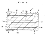
- FIG. 1 to FIG. 4 show a multilayer ceramic capacitor (hereinafter, referred to as a multilayer capacitor) 1 being an electronic component according to a first embodiment of the present invention.
- the multilayer capacitor 1 includes, as a major portion thereof, a dielectric element 3 which is a sintered compact in a rectangular parallelepiped shape obtained by sintering a multilayer body formed of a stack of a plurality of ceramic green sheets.
- the dielectric element 3 is formed of a stack of dielectric layers which are the sintered ceramic green sheets. Further, as shown in FIG. 3 and FIG. 4 , the dielectric element 3 has the internal structure such that a planar internal conductor 4 is disposed at a predetermined height position in this dielectric element 3. An internal conductor 5 similarly in a planar shape is disposed under the internal conductor 4 across a ceramic layer 3A which is the dielectric layer in the dielectric element 3. Thereafter, a plurality of layers (for example, about 100 layers) of the internal conductors 4 and the internal conductors 5 each similarly formed across the ceramic layer 3A are repeatedly arranged.
- two kinds of the internal conductors namely, the internal conductors 4 and the internal conductors 5, are arranged in the dielectric element 3 to face each other, being separated from each other by the ceramic layers 3A, as shown in FIG. 4 .
- the centers of the internal conductors 4 and the internal conductors 5 are substantially aligned with the centers of the respective ceramic layers 3A.
- the length and width dimensions of the internal conductors 4 and the internal conductors 5 are smaller than the lengths of corresponding sides of the ceramic layers 3A, respectively.
- a conductor with the same width dimension as the width dimension of the internal conductor 4 protrudes from a left side portion of each of the internal conductors 4 toward a left end of the ceramic layer 3A as shown in FIG. 3 .
- a conductor with the same width dimension as the width dimension of the internal conductor 5 protrudes from the right side portion of each of the internal conductor 5 toward the right end of the ceramic layer 3A.
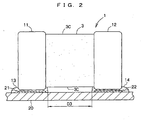
- a terminal electrode 11 connected to the left protruding portions of the internal conductors 4 is disposed on a left side face 3B that is an outer side of the dielectric element 3
- a terminal electrode 12 connected to the right protruding portions of the internal conductors 5 is disposed on a right side face 3B that is an outer side of the dielectric element 3.
- the multilayer capacitor 1 has the pair of terminal electrodes 11, 12, the pair of terminal electrodes 11, 12 being arranged on the two side faces 3B, respectively, out of four side faces of the dielectric element 3 in a rectangular parallelepiped shape of the multilayer capacitor 1. Note that when an interval dimension between the pair of terminal electrodes 11, 12 shown in FIG. 1 is defined as D, this interval dimension D is set to 500 ⁇ m or less.
- a pair of lands 21, 22 connected to the pair of terminal electrodes 11, 12 respectively are provided to face the pair of terminal electrodes 11, 12.
- a gap dimension between the pair of lands 21, 22 is defined as D1. Accordingly, the gap dimension D1 is set equal to the interval dimension D between the pair of terminal electrodes 11, 12 in this embodiment.
- the multilayer capacitor 1 When the multilayer capacitor 1 is mounted on the circuit board 20, it is necessary to connect the terminal electrode 11 to the land 21 and connect the terminal electrode 12 to the land 22. At this time, they are connected to each other in such a manner that a conductive adhesive 13 containing resin is used to bond the terminal electrode 11 to the land 21, and a conductive adhesive 14 similarly containing resin is used to bond the terminal electrode 12 to the land 22.
- the pair of conductive adhesives 13, 14 are printed on the pair of lands 21, 22 respectively, with a gap dimension D2 between the pair of conductive adhesives 13, 14 being set larger than the gap dimension D1 between the pair of lands 21, 22 by 100 ⁇ m or more.
- the multilayer capacitor 1 is mounted on the circuit board 20 while the pair of terminal electrodes 11, 12 are bonded to the pair of lands 21, 22 via the conductive adhesives 13, 14, respectively. Consequently, the structure in which the conductive adhesives 13, 14 connect therebetween is obtained.
- the multilayer capacitor 1 is structured such that the plural internal conductors 4 and the plural internal conductors 5 are arranged in the dielectric element 3 formed of a stack of the ceramic layers 3A, being separated from each other by the ceramic layers 3A.
- the pair of terminal electrodes 11, 12 are further provided on the outer sides of the dielectric element 3.
- the pair of conductive adhesives 13, 14 are printed on the pair of lands 21, 22 respectively, with the gap dimension D2 between the pair of conductive adhesives 13, 14 being wider than the gap dimension D1 between the pair of lands 21, 22 by 100 ⁇ m or more.
- the multilayer capacitor 1, which includes the pair of terminal electrodes 11, 12, with the interval dimension D therebetween being 500 ⁇ m or less, is placed on the circuit board 20, so that the multilayer capacitor 1 is mounted on the circuit board 20 while being bonded thereto via the conductive adhesives 13, 14. Therefore, the pair of terminal electrodes 11, 12 are bonded to the pair of lands 21, 22 via the conductive adhesives 13, 14 respectively, so that the multilayer capacitor 1 is mounted on the circuit board 20.
- an excessive amount of the conductive adhesives 13, 14 or an excessively high pressure for mounting the multilayer capacitor 1 on the circuit board 20 cause the conductive adhesives 13, 14 to be crushed and spread between the terminal electrodes 11, 12 of the multilayer capacitor 1 and the circuit board 20.
- the conductive adhesives 13, 14 spread toward outer sides of the pair of lands 21, 22 as shown in FIG. 2 since the conductive adhesives 13, 14 are not printed on portions of the pair of lands 21, 22 on a side where the pair of lands 21, 22 face each other as shown in FIG. 1 . Consequently, the occurrence of short or ion migration caused by the conductive adhesives 13, 14 is prevented in this embodiment.
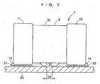
- FIG. 5 An electronic component mounting method and an electronic component mounting structure according to a second embodiment of the present invention will be described based on FIG. 5 .
- the same reference numerals and symbols are used to designate the same members as those described in the first embodiment, and repeated description thereof will be omitted.
- This embodiment is also structured, similarly to the first embodiment, such that a multilayer capacitor 1 includes a pair of terminal electrodes 11, 12, and an interval dimension D ⁇ m between the pair of terminal electrodes 11, 12 is set to 500 ⁇ m or less.
- the gap dimension D2 between the pair of conductive adhesives 13, 14 is made wider than the gap dimension D1 between the pair of lands 21, 22 by 100 ⁇ m or more.
- the pair of terminal electrodes 11, 12 are formed to satisfy the relation that H ⁇ D is 4000 or more, where H ⁇ m is a thickness dimension of portions of the terminal electrodes 11, 12 facing the lands 21, 22, and D ⁇ m is an interval dimension between the pair of terminal electrodes 11, 12.
- the conductive adhesives 13, 14 are first printed on the pair of lands 21, 22 respectively. After this printing, the multilayer capacitor 1 having the pair of terminal electrodes 11, 12 that are formed in the above-described manner is mounted on the circuit board 20 while being bonded thereto via the conductive adhesives 13, 14. Therefore, also in this embodiment, the pair of terminal electrodes 11, 12 are bonded to the pair lands 21, 22 via the conductive adhesives 13, 14 respectively, so that the multilayer capacitor 1 is mounted on the circuit board 20.
- this embodiment prevents the occurrence of the aforementioned problem of short or the like as a result of forming the pair of terminal electrodes 11, 12 such that H ⁇ D, which is a product of the thickness dimension H ⁇ m of the portions of the terminal electrodes 11, 12 facing the lands 21, 22 and the interval dimension D ⁇ m between the pair of terminal electrodes 11, 12, is 4000 or more.
- an interval dimension S between a portion sandwiched by the pair of terminal electrodes 11, 12 in the multilayer capacitor 1 and the circuit board 20 is widened, so that the conductive adhesives 13, 14 do not spread more than necessary even when the conductive adhesives 13, 14 are crushed between the terminal electrodes 11, 12 of the multilayer capacitor 1 and the circuit board 20. Consequently, this embodiment also prevents the occurrence of short or ion migration.
- the gap dimension D2 between the pair of conductive adhesives 13, 14 was made larger than the interval dimension D between the pair of terminal electrodes 11, 12 and the gap dimension D1 between the pair of lands 21, 22 by 100 ⁇ m or more and not more than 150 ⁇ m.
- Nine kinds of samples were also prepared as comparative examples 1 to 9. In these nine samples, the gap dimension D2 was not wider than the interval dimension D and the gap dimension D 1 by 100 ⁇ m or more.
- interval dimension D and gap dimension D1 were set equal to each other, and the interval dimension D and the gap dimension D1 were set to 500 ⁇ m or less in all the samples.
- the interval dimension D and the gap dimension D 1 were set to four different kinds of values, namely, 500 ⁇ m, 400 ⁇ m, 300 ⁇ m, and 200 ⁇ m, and the gap dimension D2 between the conductive adhesives 13, 14 after being printed was set to 600 ⁇ m to 200 ⁇ m. Further, the printed thickness of the conductive adhesives 13, 14 was 25 ⁇ 10 ⁇ m.
- evaluation items were defined as evaluation items in Table 1, namely, the gap dimension D3 between the conductive adhesives 13, 14 after mount (in Table 1, noted as conductive adhesive gap dimension D3 after mount), electric characteristic after mount, PCBT result, and moisture resistance cycle test result.
- the electric characteristic after mount among these evaluation items was the result of confirming the respective electric characteristics of Cp, tan ⁇ , and IR after mount.
- the PCBT result was obtained under a high-temperature, high humidity, and high pressure condition of 121°C, 95% RH, and 2 atmW.V./100 hr.
- OK represents that a predetermined standard was satisfied and NG represents that the predetermined standard was not satisfied.
- the gap dimension D3 between the conductive adhesives 13, 14 after mount in the examples 1 to 7 was substantially equal to the original gap dimension D2.
- the gap dimension D3 between the conductive adhesives 13, 14 after mount in the comparative examples 1 to 9 became significantly smaller than the original gap dimension D2. Accordingly, the comparative samples 7, 9 in which the gap dimension D3 became zero were evaluated as NG in the electric characteristic after mount.
- the comparative examples 2, 3, 5, 8 in which the gap dimension D3 between the conductive adhesives 13, 14 after mount was 150 ⁇ m or less were evaluated as NG in the PCBT result.
- the comparative examples 1 to 6 and 8 with a narrow gap dimension D3 were evaluated as NG. Note that no evaluation on the PCBT result and the moisture resistance cycle test result was made for the comparative examples 7, 9 that were evaluated as NG in the electric characteristic after mount.
- the examples 1 to 7 had no problem since they were all evaluated as OK as the results of the respective test items, but the comparative examples 1 to 9 were evaluated as NG in some test items. Therefore, from the results shown in Table 1, it was confirmed that the gap dimension D2 between the pair of conductive adhesives 13, 14 has to be larger than the gap dimension D1 between the pair of lands 21, 22 by 100 ⁇ m or more when they are printed.
- H ⁇ D which is the product of the thickness dimension H ⁇ m of the portions of the pair of terminal electrodes 11, 12 facing the pair of lands 21, 22 respectively and the interval dimension D ⁇ m between the pair of terminal electrodes 11, 12, was set to 4000 or more and not more than 5000. Eight samples in which H ⁇ D was set to less than 4000 were also prepared as comparative examples 10 to 17.
- interval dimension D and the gap dimension D1 were set equal to each other. Further, the interval dimension D and the gap dimension D1 were set to 500 ⁇ m or less in all the samples. Specifically, the interval dimension D and the gap dimension D 1 were set to four different kinds of values, namely, 500 ⁇ m, 400 ⁇ m, 300 ⁇ m, and 200 ⁇ m, and the thickness dimension H was set to 5 ⁇ m to 20 ⁇ m.
- the gap dimension D3 between the conductive adhesives 13, 14 after mount was 160 ⁇ m or less in all the comparative examples 10 to 17. Accordingly, the comparative examples 12, 16 in which the gap dimension D3 between the conductive adhesives 13, 14 after mount was zero were evaluated as NG in the electric characteristic after mount.
- the comparative examples 10, 13, 14 in which the gap dimension D3 between the conductive adhesives 13, 14 after mount was 150 ⁇ m or less were evaluated as NG in the PCBT result.
- the comparative examples 10, 11, 13 to 15, 17 each having a narrow gap dimension D3 were evaluated as NG also in the moisture resistance cycle test result. Note that no evaluation on the PCBT result and moisture resistance cycle test result was made for the comparative examples 12, 16 evaluated as NG in the electric characteristic after mount.
- H ⁇ D which is the product of the thickness dimension H ⁇ m of the portions of the pair of terminal electrodes 11, 12 facing the pair of lands 21, 22 respectively and the interval dimension D ⁇ m between the pair of terminal electrodes 11, 12, has to be set to 4000 or more.
- the conductive adhesives used in the above-described embodiments it is conceivable to adopt known conductive adhesives as the conductive adhesives used in the above-described embodiments. Further, viscosity of paste for terminal electrodes may be changed or the number of times of immersing the terminal electrodes in the paste may be increased in order to increase the thickness of the terminal electrodes. Moreover, the number of the internal conductors of the multilayer capacitor 1 is not limited to that in the multilayer capacitor 1 according to the above-described embodiments, but may be larger. Further, the order of the internal conductors in the layering direction may be arbitrarily changed.
- the present invention it is possible to obtain an electronic component mounting method and an electronic component mounting structure that prevent the occurrence of short or ion migration even when a conductive adhesive is crushed between an electronic component and a circuit board.
- the present invention is particularly suitable for use in mounting a multilayer ceramic capacitor on a circuit board.
Landscapes
- Engineering & Computer Science (AREA)
- Power Engineering (AREA)
- Microelectronics & Electronic Packaging (AREA)
- Manufacturing & Machinery (AREA)
- Electric Connection Of Electric Components To Printed Circuits (AREA)
- Ceramic Capacitors (AREA)
- Fixed Capacitors And Capacitor Manufacturing Machines (AREA)
- Structures For Mounting Electric Components On Printed Circuit Boards (AREA)
Claims (6)
- Elektronisches Bauteilmontierungsverfahren zum Montieren eines elektronischen Bauteils (1), welches ein Paar terminale Elektroden (11, 12) mit einer dazwischen liegenden Abstandsdimension auf einer Platine (20) durch Binden des Paares der terminalen Elektroden (11, 12) jeweils auf ein Paar von Anschlussflächen (21, 22) auf der Platine (20) über leitende Klebemittel (13, 14) beinhaltet,
dadurch gekennzeichnet, dass
das Paar leitende Klebemittel (13, 14) das Anschlussflächenpaar (21, 22) mit einer gedruckten Dickendimension von 25 ± 10 µm mit einer Abstandsdimension zwischen dem Paar der leitenden Klebemittel (13, 14), die größer sind als die Abstandsdimension zwischen dem Paar der Anschlussflächen (21, 22) von 100 bis 150 µm, und wobei das elektronische Bauteil (1) auf der Platine (20) anschließend montiert wird, während es auf die Platine (20) über die leitenden Klebemittel (13, 14) gebunden wird, und wobei die Abstandsdimension zwischen dem Paar der leitenden Klebemittel (13, 14) 200 µm oder mehr nach dem Montieren ist. - Elektronisches Bauteilmontierungsverfahren zum Montieren eines elektronischen Bauteils (1), welches ein Paar terminale Elektroden (11, 12) mit einer dazwischen liegenden Abstandsdimension auf einer Platine (20) durch Binden des Paares der terminalen Elektroden (11, 12) jeweils auf ein Paar von Anschlussflächen (21, 22) auf der Platine (20) über leitende Klebemittel (13, 14) beinhaltet,
dadurch gekennzeichnet, dass
das Paar der terminalen Elektroden (11, 12) so ausgebildet ist, um einer Beziehung zu genügen, in der H 10 bis 20 µm ist und H x D einen Wert in einem Bereich von 4000 bis 5000 ergibt, worin H µm eine Dickendimension der Abschnitte der terminalen Elektronen (11, 12) ist, die den Anschlussflächen (21, 22) zugewandt ist, und D µm eine Abstandsdimension zwischen dem Paar der terminalen Elektronen (11, 12) ist, und
nachdem die leitenden Klebemittel (13, 14) als nächstes auf das Paar der Anschlussflächen (21, 22) jeweils gedruckt worden sind, das elektronische Bauteil (1) auf der Platine montiert wird, während es auf der Platine (20) über die leitenden Klebemittel (13, 14) gebunden ist und worin die Abstandsdimension zwischen dem Paar der leitenden Klebemittel (13, 14) 180 µm oder mehr nach dem Montieren ist. - Elektronische Bauteilmontierstruktur, in welcher ein elektronisches Bauteil (1), welches jeweils ein Paar terminale Elektroden (11, 12) mit einer Abstandsdimension dazwischen auf eine Platine (20) durch Binden des Paares der terminalen Elektroden (11, 12) jeweils auf ein Paar von Anschlussflächen (21, 22) auf die Platine (20) über leitende Klebemittel (13, 14) beinhaltet,
dadurch gekennzeichnet, dass
das Paar der terminalen Elektroden (11, 12) so ausgebildet ist, um einer Beziehung zu genügen, in der H 10 bis 20 µm ist und H x D einen Wert in einem Bereich von 4000 bis 5000 ergibt, worin H µm eine Dickendimension der Abschnitte der terminalen Elektronen (11, 12) ist, die den Anschlussflächen (21, 22) zugewandt ist, und D µm die Abstandsdimension zwischen dem Paar der terminalen Elektronen (11, 12) ist, und
das elektronische Bauteil (1) auf der Platine (20) montiert ist, während es auf der Platine (20) über die leitenden Klebemittel (13, 14) gebunden ist und worin die Abstandsdimension zwischen dem Paar der leitenden Klebemittel (13, 14) 180 µm oder mehr nach dem Montieren ist. - Elektronische Bauteilmontierstruktur nach Anspruch 3,
dadurch gekennzeichnet, dass
das elektronische Bauteil (1) ein vielschichtiges Keramikkondensatorgehäuse ist, das zwei Arten interner Innenkondensatoren (4, 5) aufnimmt, wobei der Innenkondensator der einen Art mit einem Paar der terminalen Elektroden (11, 12) verbunden ist und der Innenkondensator der anderen Art mit der anderen terminalen Elektrode verbunden ist. - Elektronische Bauteilmontierstruktur nach Anspruch 3,
dadurch gekennzeichnet, dass
ein größerer Teil des elektronischen Bauteils (1) als ein Stapel dielektrischer Schichten, die keramische Schichten (3A) sind, und in Gestalt eines rechtwinkligen Parallelepipeds ausgebildet ist. - Elektronische Bauteilmontierstruktur nach Anspruch 3,
dadurch gekennzeichnet, dass
die leitenden Klebemittel (13, 14) Harz enthalten.
Applications Claiming Priority (2)
| Application Number | Priority Date | Filing Date | Title |
|---|---|---|---|
| JP2003337386 | 2003-09-29 | ||
| JP2003337386A JP2005108966A (ja) | 2003-09-29 | 2003-09-29 | 電子部品の実装方法 |
Publications (2)
| Publication Number | Publication Date |
|---|---|
| EP1519642A1 EP1519642A1 (de) | 2005-03-30 |
| EP1519642B1 true EP1519642B1 (de) | 2011-11-09 |
Family
ID=34191567
Family Applications (1)
| Application Number | Title | Priority Date | Filing Date |
|---|---|---|---|
| EP04022698A Expired - Lifetime EP1519642B1 (de) | 2003-09-29 | 2004-09-23 | Verfahren und Struktur zur Montierung eines elektronischen Bauteils |
Country Status (4)
| Country | Link |
|---|---|
| EP (1) | EP1519642B1 (de) |
| JP (1) | JP2005108966A (de) |
| CN (1) | CN100585760C (de) |
| TW (1) | TWI328414B (de) |
Families Citing this family (9)
| Publication number | Priority date | Publication date | Assignee | Title |
|---|---|---|---|---|
| JP2007005769A (ja) * | 2005-05-27 | 2007-01-11 | Tdk Corp | コイル部品及び電子機器 |
| WO2009001842A1 (ja) * | 2007-06-27 | 2008-12-31 | Murata Manufacturing Co., Ltd. | 積層セラミック電子部品及びその実装構造 |
| JP5402107B2 (ja) * | 2009-03-10 | 2014-01-29 | 日本電気株式会社 | 半導体装置及びその製造方法 |
| KR101548773B1 (ko) * | 2011-08-22 | 2015-08-31 | 삼성전기주식회사 | 적층 세라믹 커패시터의 회로 기판 실장 구조 |
| KR101862422B1 (ko) * | 2013-06-14 | 2018-05-29 | 삼성전기주식회사 | 적층 세라믹 커패시터 및 그 실장 기판 |
| JP6011574B2 (ja) * | 2013-06-27 | 2016-10-19 | 株式会社村田製作所 | 積層セラミックコンデンサ |
| JP5958479B2 (ja) * | 2014-01-31 | 2016-08-02 | 株式会社村田製作所 | 電子部品の実装構造体 |
| JP7292958B2 (ja) * | 2019-04-26 | 2023-06-19 | 株式会社村田製作所 | 電子部品の実装構造体 |
| JPWO2024062605A1 (de) * | 2022-09-22 | 2024-03-28 |
Family Cites Families (6)
| Publication number | Priority date | Publication date | Assignee | Title |
|---|---|---|---|---|
| JPH06177526A (ja) * | 1992-12-09 | 1994-06-24 | Toyota Autom Loom Works Ltd | 接合剤の印刷方法 |
| JPH06216509A (ja) * | 1993-01-12 | 1994-08-05 | Sony Corp | 電子部品 |
| JPH1154894A (ja) * | 1997-08-05 | 1999-02-26 | Fujitsu Ten Ltd | 電子部品の実装方法及び電子部品の実装構造並びに電子部品の構造 |
| US6012231A (en) * | 1997-12-08 | 2000-01-11 | Micron Technology, Inc. | Soldered integrated circuit connections |
| JP2001102715A (ja) * | 1999-09-30 | 2001-04-13 | Fujitsu General Ltd | 導電性接着剤用部品構造 |
| JP2002124748A (ja) * | 2000-10-12 | 2002-04-26 | Ngk Insulators Ltd | 回路素子実装基板及び回路素子実装方法 |
-
2003
- 2003-09-29 JP JP2003337386A patent/JP2005108966A/ja active Pending
-
2004
- 2004-09-23 EP EP04022698A patent/EP1519642B1/de not_active Expired - Lifetime
- 2004-09-27 TW TW093129172A patent/TWI328414B/zh not_active IP Right Cessation
- 2004-09-29 CN CN200410083153A patent/CN100585760C/zh not_active Expired - Lifetime
Also Published As
| Publication number | Publication date |
|---|---|
| JP2005108966A (ja) | 2005-04-21 |
| EP1519642A1 (de) | 2005-03-30 |
| TWI328414B (en) | 2010-08-01 |
| TW200528000A (en) | 2005-08-16 |
| CN1604244A (zh) | 2005-04-06 |
| CN100585760C (zh) | 2010-01-27 |
Similar Documents
| Publication | Publication Date | Title |
|---|---|---|
| EP1508905B1 (de) | Elektronisches Bauteil | |
| JP3322199B2 (ja) | 多層セラミック基板およびその製造方法 | |
| KR101963273B1 (ko) | 인터포저, 인터포저를 포함하는 전자 부품 및 인터포저를 포함하는 전자 부품의 실장 기판 | |
| US5495387A (en) | RC array | |
| US10141116B2 (en) | Composite electronic component and resistor device | |
| EP1519642B1 (de) | Verfahren und Struktur zur Montierung eines elektronischen Bauteils | |
| JPH0632378B2 (ja) | 電子部品内蔵多層セラミック基板 | |
| JPH0897070A (ja) | セラミックコンデンサ | |
| JPH1140459A (ja) | 複合電子部品 | |
| KR102145316B1 (ko) | 적층 세라믹 커패시터 및 그 실장 기판 | |
| JP2946261B2 (ja) | 積層電子部品の製造方法 | |
| JPH0878991A (ja) | チップ型lcフィルタ素子 | |
| JP2002343640A (ja) | 積層セラミック型電子部品 | |
| KR100672235B1 (ko) | 바리스터 및 그 제조 방법 | |
| JP4766292B2 (ja) | 非可逆回路素子 | |
| KR20140148157A (ko) | 적층 세라믹 전자 부품의 제조 방법 및 이를 이용하여 제조된 적층 세라믹 전자 부품 | |
| JPH04267317A (ja) | 積層セラミックコンデンサ | |
| JPH1155058A (ja) | 積層セラミック複合部品 | |
| JP3418874B2 (ja) | 積層複合電子部品 | |
| JP2607716Y2 (ja) | 積層lcフィルタと回路基板との実装構造 | |
| KR200408406Y1 (ko) | 칩 배리스터 | |
| JPH03266410A (ja) | Cr複合素子 | |
| KR20250134501A (ko) | 적층 세라믹 전자부품 | |
| JPH0214505A (ja) | コンデンサアレイ | |
| JP3005615U (ja) | コンデンサアレー |
Legal Events
| Date | Code | Title | Description |
|---|---|---|---|
| PUAI | Public reference made under article 153(3) epc to a published international application that has entered the european phase |
Free format text: ORIGINAL CODE: 0009012 |
|
| AK | Designated contracting states |
Kind code of ref document: A1 Designated state(s): AT BE BG CH CY CZ DE DK EE ES FI FR GB GR HU IE IT LI LU MC NL PL PT RO SE SI SK TR |
|
| AX | Request for extension of the european patent |
Extension state: AL HR LT LV MK |
|
| 17P | Request for examination filed |
Effective date: 20050530 |
|
| AKX | Designation fees paid |
Designated state(s): DE FR IT |
|
| 17Q | First examination report despatched |
Effective date: 20100607 |
|
| GRAP | Despatch of communication of intention to grant a patent |
Free format text: ORIGINAL CODE: EPIDOSNIGR1 |
|
| GRAS | Grant fee paid |
Free format text: ORIGINAL CODE: EPIDOSNIGR3 |
|
| GRAA | (expected) grant |
Free format text: ORIGINAL CODE: 0009210 |
|
| AK | Designated contracting states |
Kind code of ref document: B1 Designated state(s): DE FR IT |
|
| REG | Reference to a national code |
Ref country code: DE Ref legal event code: R096 Ref document number: 602004035199 Country of ref document: DE Effective date: 20120119 |
|
| PG25 | Lapsed in a contracting state [announced via postgrant information from national office to epo] |
Ref country code: IT Free format text: LAPSE BECAUSE OF FAILURE TO SUBMIT A TRANSLATION OF THE DESCRIPTION OR TO PAY THE FEE WITHIN THE PRESCRIBED TIME-LIMIT Effective date: 20111109 |
|
| PLBE | No opposition filed within time limit |
Free format text: ORIGINAL CODE: 0009261 |
|
| STAA | Information on the status of an ep patent application or granted ep patent |
Free format text: STATUS: NO OPPOSITION FILED WITHIN TIME LIMIT |
|
| 26N | No opposition filed |
Effective date: 20120810 |
|
| REG | Reference to a national code |
Ref country code: DE Ref legal event code: R097 Ref document number: 602004035199 Country of ref document: DE Effective date: 20120810 |
|
| REG | Reference to a national code |
Ref country code: FR Ref legal event code: ST Effective date: 20130531 |
|
| PG25 | Lapsed in a contracting state [announced via postgrant information from national office to epo] |
Ref country code: FR Free format text: LAPSE BECAUSE OF NON-PAYMENT OF DUE FEES Effective date: 20121001 |
|
| REG | Reference to a national code |
Ref country code: DE Ref legal event code: R082 Ref document number: 602004035199 Country of ref document: DE Representative=s name: PATENTANWAELTE WEICKMANN & WEICKMANN, DE Ref country code: DE Ref legal event code: R082 Ref document number: 602004035199 Country of ref document: DE Representative=s name: WEICKMANN & WEICKMANN PATENTANWAELTE - RECHTSA, DE Ref country code: DE Ref legal event code: R082 Ref document number: 602004035199 Country of ref document: DE Representative=s name: WEICKMANN & WEICKMANN PATENT- UND RECHTSANWAEL, DE |
|
| PGFP | Annual fee paid to national office [announced via postgrant information from national office to epo] |
Ref country code: DE Payment date: 20230802 Year of fee payment: 20 |
|
| REG | Reference to a national code |
Ref country code: DE Ref legal event code: R071 Ref document number: 602004035199 Country of ref document: DE |