EP1519231B1 - Appareil lithographique et procédé pour la production d'un dispositif - Google Patents
Appareil lithographique et procédé pour la production d'un dispositif Download PDFInfo
- Publication number
- EP1519231B1 EP1519231B1 EP03256096A EP03256096A EP1519231B1 EP 1519231 B1 EP1519231 B1 EP 1519231B1 EP 03256096 A EP03256096 A EP 03256096A EP 03256096 A EP03256096 A EP 03256096A EP 1519231 B1 EP1519231 B1 EP 1519231B1
- Authority
- EP
- European Patent Office
- Prior art keywords
- substrate
- time
- target portion
- immersion liquid
- projection
- Prior art date
- Legal status (The legal status is an assumption and is not a legal conclusion. Google has not performed a legal analysis and makes no representation as to the accuracy of the status listed.)
- Expired - Fee Related
Links
- 238000004519 manufacturing process Methods 0.000 title claims description 7
- 239000007788 liquid Substances 0.000 claims description 104
- 239000000758 substrate Substances 0.000 claims description 98
- 238000007654 immersion Methods 0.000 claims description 54
- 230000005855 radiation Effects 0.000 claims description 22
- 238000000059 patterning Methods 0.000 claims description 19
- 238000005286 illumination Methods 0.000 claims description 6
- 238000000034 method Methods 0.000 claims 3
- 229920002120 photoresistant polymer Polymers 0.000 description 18
- 238000003384 imaging method Methods 0.000 description 8
- 230000003287 optical effect Effects 0.000 description 7
- 238000004090 dissolution Methods 0.000 description 6
- 239000010410 layer Substances 0.000 description 5
- 230000000694 effects Effects 0.000 description 4
- 238000009792 diffusion process Methods 0.000 description 3
- 238000000671 immersion lithography Methods 0.000 description 3
- 238000004364 calculation method Methods 0.000 description 2
- 238000001459 lithography Methods 0.000 description 2
- 230000010363 phase shift Effects 0.000 description 2
- 230000003068 static effect Effects 0.000 description 2
- XUIMIQQOPSSXEZ-UHFFFAOYSA-N Silicon Chemical compound [Si] XUIMIQQOPSSXEZ-UHFFFAOYSA-N 0.000 description 1
- 238000004458 analytical method Methods 0.000 description 1
- 238000003491 array Methods 0.000 description 1
- 230000002238 attenuated effect Effects 0.000 description 1
- 230000001143 conditioned effect Effects 0.000 description 1
- 238000012937 correction Methods 0.000 description 1
- 230000003247 decreasing effect Effects 0.000 description 1
- 230000001419 dependent effect Effects 0.000 description 1
- 238000001514 detection method Methods 0.000 description 1
- 230000009977 dual effect Effects 0.000 description 1
- 230000005670 electromagnetic radiation Effects 0.000 description 1
- 239000012530 fluid Substances 0.000 description 1
- 230000006870 function Effects 0.000 description 1
- 238000001802 infusion Methods 0.000 description 1
- 238000007689 inspection Methods 0.000 description 1
- 239000002346 layers by function Substances 0.000 description 1
- 239000004973 liquid crystal related substance Substances 0.000 description 1
- 230000005381 magnetic domain Effects 0.000 description 1
- 239000000463 material Substances 0.000 description 1
- 239000011159 matrix material Substances 0.000 description 1
- 238000005259 measurement Methods 0.000 description 1
- 230000015654 memory Effects 0.000 description 1
- QSHDDOUJBYECFT-UHFFFAOYSA-N mercury Chemical compound [Hg] QSHDDOUJBYECFT-UHFFFAOYSA-N 0.000 description 1
- 229910052753 mercury Inorganic materials 0.000 description 1
- 238000012545 processing Methods 0.000 description 1
- 210000001747 pupil Anatomy 0.000 description 1
- 238000007493 shaping process Methods 0.000 description 1
- 229910052710 silicon Inorganic materials 0.000 description 1
- 239000010703 silicon Substances 0.000 description 1
- 239000010409 thin film Substances 0.000 description 1
- XLYOFNOQVPJJNP-UHFFFAOYSA-N water Substances O XLYOFNOQVPJJNP-UHFFFAOYSA-N 0.000 description 1
Images
Classifications
-
- G—PHYSICS
- G03—PHOTOGRAPHY; CINEMATOGRAPHY; ANALOGOUS TECHNIQUES USING WAVES OTHER THAN OPTICAL WAVES; ELECTROGRAPHY; HOLOGRAPHY
- G03F—PHOTOMECHANICAL PRODUCTION OF TEXTURED OR PATTERNED SURFACES, e.g. FOR PRINTING, FOR PROCESSING OF SEMICONDUCTOR DEVICES; MATERIALS THEREFOR; ORIGINALS THEREFOR; APPARATUS SPECIALLY ADAPTED THEREFOR
- G03F7/00—Photomechanical, e.g. photolithographic, production of textured or patterned surfaces, e.g. printing surfaces; Materials therefor, e.g. comprising photoresists; Apparatus specially adapted therefor
- G03F7/70—Microphotolithographic exposure; Apparatus therefor
- G03F7/70216—Mask projection systems
- G03F7/70341—Details of immersion lithography aspects, e.g. exposure media or control of immersion liquid supply
Definitions
- the present invention relates to a lithographic apparatus and a device manufacturing method.
- a lithographic apparatus is a machine that applies a desired pattern onto a target portion of a substrate.
- Lithographic apparatus can be used, for example, in the manufacture of integrated circuits (ICs).
- a patterning means such as a mask, may be used to generate a circuit pattern corresponding to an individual layer of the IC, and this pattern can be imaged onto a target portion (e.g. comprising part of, one or several dies) on a substrate (e.g. a silicon wafer) that has a layer of radiation-sensitive material (resist).
- a single substrate will contain a network of adjacent target portions that are successively exposed.
- lithographic apparatus include so-called steppers, in which each target portion is irradiated by exposing an entire pattern onto the target portion in one go, and so-called scanners, in which each target portion is irradiated by scanning the pattern through the projection beam in a given direction (the "scanning"-direction) while synchronously scanning the substrate parallel or anti-parallel to this direction.
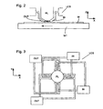
- liquid supply system to provide liquid on only a localized area of the substrate and in between the final element of the projection system and the substrate using a liquid confinement system LCS (the substrate generally has a larger surface area than the final element of the projection system).
- LCS liquid confinement system
- liquid is supplied by at least one inlet IN onto the substrate, preferably along the direction of movement of the substrate relative to the final element, and is removed by at least one outlet OUT after having passed under the projection system. That is, as the substrate is scanned beneath the element in a -X direction, liquid is supplied at the +X side of the element and taken up at the -X side.
- Figure 2 shows the arrangement schematically in which liquid is supplied via inlet IN and is taken up on the other side of the element by outlet OUT which is connected to a low pressure source.
- the liquid is supplied along the direction of movement of the substrate relative to the final element, though this does not need to be the case.
- Figure 3 shows the arrangement schematically in which liquid is supplied via inlet IN and is taken up on the other side of the element by outlet OUT which is connected to a low pressure source.
- Another localized area solution which has been proposed is to provide the liquid supply system with a seal member which extends along at least a part of a boundary of the space between the final element of the projection system and the substrate table.
- the seal member is substantially stationary relative to the projection system in the XY plane though there may be some relative movement in the Z direction (in the direction of the optical axis).
- a seal is formed between the seal member and the surface of the substrate.
- the seal is a contactless seal such as a gas seal.
- a lithographic apparatus comprising:
- the apparatus can account for dissolution of the photoresist on the surface of the substrate in the immersion liquid and/or diffusion of immersion liquid into the resist.
- the problem is that as the photoresist dissolves, the characteristics of the effect of impingement of the patterned beam on the target portion changes, so that there is a change in the critical dimension achievable with time of contact with immersion liquid.
- the apparatus of the present invention solves this problems in one of two ways; either the apparatus ensures that each part of the substrate which is to be imaged (i.e. each target portion) is immersed in immersion liquid for substantially the same amount of time or the apparatus takes into account how long the target portion of the substrate has been immersed in immersion liquid and applies a correction to the projected patterned beam to account for this.
- the intensity or duration of projection of the patterned beam on that target portion will need to be increased or decreased according to the particular circumstance (e.g. type of feature, type of immersion liquid, type of resist etc.). If the target portion has been immersed less than average, the projected patterned beam will also need to be adjusted.
- One way for the controller to ensure that the apparatus compensates for critical dimension changing due to immersion of the photoresist in immersion liquid is by operating the apparatus by moving the substrate such that each target portion on the substrate has immersion liquid provided by said liquid supply system on it for said substantially equal length of time.
- the path of the substrate under the projection system which is chosen ensures that the substrate meanders under the projection system PL such that each target portion is part of the localized area for the same amount of time as all other target portions.
- Another way of ensuring that each target portion is immersed for the same amount of time in immersion liquid is to provide a supplementary liquid supply system for providing immersion liquid to said substrate outside of the localized area and wherein said controller is for operating the apparatus by applying the immersion liquid outside of the localized area using the supplementary liquid supply system.
- target portions which, for some reason, are under the projection system and thereby immersed in immersion liquid by the liquid supply system less than average, can have their exposure to immersion liquid "topped up" to the required level by use of the supplementary liquid supply system.
- a device manufacturing method comprising the steps of:
- lithographic apparatus in the manufacture of ICs, it should be understood that the lithographic apparatus described herein may have other applications, such as the manufacture of integrated optical systems, guidance and detection patterns for magnetic domain memories, liquid-crystal displays (LCDs), thin-film magnetic heads, etc.
- LCDs liquid-crystal displays
- any use of the terms “wafer” or “die” herein may be considered as synonymous with the more general terms “substrate” or "target portion”, respectively.
- the substrate referred to herein may be processed, before or after exposure, in for example a track (a tool that typically applies a layer of resist to a substrate and develops the exposed resist) or a metrology or inspection tool.
- the disclosure herein may be applied to such and other substrate processing tools.
- the substrate may be processed more than once, for example in order to create a multi-layer IC, so that the term substrate used herein may also refer to a substrate that already contains multiple processed layers.
- UV radiation e.g. having a wavelength of 365, 248, 193, 157 or 126 nm.
- patterning means used herein should be broadly interpreted as referring to means that can be used to impart a projection beam with a pattern in its cross-section such as to create a pattern in a target portion of the substrate. It should be noted that the pattern imparted to the projection beam may not exactly correspond to the desired pattern in the target portion of the substrate. Generally, the pattern imparted to the projection beam will correspond to a particular functional layer in a device being created in the target portion, such as an integrated circuit.
- Patterning means may be transmissive or reflective.
- Examples of patterning means include masks, programmable mirror arrays, and programmable LCD panels.
- Masks are well known in lithography, and include mask types such as binary, alternating phase-shift, and attenuated phase-shift, as well as various hybrid mask types.
- An example of a programmable mirror array employs a matrix arrangement of small mirrors, each of which can be individually tilted so as to reflect an incoming radiation beam in different directions; in this manner, the reflected beam is patterned.
- the support structure may be a frame or table, for example, which may be fixed or movable as required and which may ensure that the patterning means is at a desired position, for example with respect to the projection system. Any use of the terms "reticle” or “mask” herein may be considered synonymous with the more general term "patterning means”.
- projection system used herein should be broadly interpreted as encompassing various types of projection system, including refractive optical systems, reflective optical systems, and catadioptric optical systems, as appropriate for example for the exposure radiation being used, or for other factors such as the use of an immersion fluid or the use of a vacuum. Any use of the term “lens” herein may be considered as synonymous with the more general term “projection system”.
- the illumination system may also encompass various types of optical components, including refractive, reflective, and catadioptric optical components for directing, shaping, or controlling the projection beam of radiation, and such components may also be referred to below, collectively or singularly, as a "lens”.
- the lithographic apparatus may be of a type having two (dual stage) or more substrate tables (and/or two or more mask tables). In such "multiple stage” machines the additional tables may be used in parallel, or preparatory steps may be carried out on one or more tables while one or more other tables are being used for exposure.
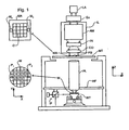
- Figure 1 schematically depicts a lithographic apparatus according to a particular embodiment of the invention.
- the apparatus comprises:
- the illuminator IL receives a beam of radiation from a radiation source SO.
- the source and the lithographic apparatus may be separate entities, for example when the source is an excimer laser. In such cases, the source is not considered to form part of the lithographic apparatus and the radiation beam is passed from the source SO to the illuminator IL with the aid of a beam delivery system BD comprising for example suitable directing mirrors and/or a beam expander. In other cases the source may be integral part of the apparatus, for example when the source is a mercury lamp.
- the source SO and the illuminator IL, together with the beam delivery system BD if required, may be referred to as a radiation system.
- the illuminator IL may comprise adjusting means AM for adjusting the angular intensity distribution of the beam.
- adjusting means AM for adjusting the angular intensity distribution of the beam.
- the illuminator IL generally comprises various other components, such as an integrator IN and a condenser CO.
- the illuminator provides a conditioned beam of radiation, referred to as the projection beam PB, having a desired uniformity and intensity distribution in its cross-section.
- the projection beam PB is incident on the mask MA, which is held on the mask table MT. Having traversed the mask MA, the projection beam PB passes through the lens PL, which focuses the beam onto a target portion C of the substrate W.
- the substrate table WT can be moved accurately, e.g. so as to position different target portions C in the path of the beam PB.
- the first positioning means PM and another position sensor can be used to accurately position the mask MA with respect to the path of the beam PB, e.g. after mechanical retrieval from a mask library, or during a scan.
- the mask table MT may be connected to a short stroke actuator only, or may be fixed.
- Mask MA and substrate W may be aligned using mask alignment marks M1, M2 and substrate alignment marks P1, P2.
- the present invention relates to immersion lithography in which a space between the final element of the projection system and the substrate is at least partly filled with immersion liquid.
- a unique problem with immersion lithography has been found by the present inventors to be present in the types of system which use a liquid supply system which supplies liquid to only a localized area of the substrate.
- Two examples of such localized liquid supply systems are described in WO99/ 49504 and European Patent Application No. 03252955.4 both hereby incorporated in their entirety by reference.
- the present invention is applied to any type of localized area liquid supply system.
- the present inventors have found that a problem occurs with localized liquid supply systems if areas of the substrate are in contact with the immersion liquid for different amounts of time. This problem results because the photoresist which covers the substrate W dissolves or reacts with the immersion liquid with time and immersion liquid diffuses into the photoresist with time so that the properties of the photoresist change with time of immersion. A target portion which has been in contact with immersion liquid for longer than another target portion will be patterned differently under the same exposure conditions. This has not been a problem with previous types of immersion apparatus such as those in which the whole substrate or substrate table are placed in a bath of liquid (see US 4,509,825 for example).
- One of the solutions of the present invention is to use a controller to ensure that all areas of the substrate W which are to be imaged (i.e. all target portions) are covered in immersion liquid for a substantially equal length of time. Dissolution of the photoresist occurs both during imaging as well as after imaging. Diffusion of immersion liquid into the photoresist occurs both before, during and after imaging.
- the controller needs to operate the apparatus such that all target portions of the substrate have the immersion liquid on them for substantially equal length of time, perhaps even equal amounts of time before, equal amounts of time during and equal amounts of time after imaging.
- One way of doing this is to choose a path of the substrate under the projection system PL to ensure that the criterion is met.
- This path is unlikely to be the optimal path which maximizes throughput of substrates but this disadvantage is more than offset by the fact that all target portions can have the same exposure dose of projection beam which can be chosen for the particular pattern to be imaged and type of photoresist, duration of immersion, pattern to be imaged, wavelength etc.
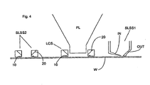
- a liquid supply system which has a liquid confinement system LCS is positioned around the final element of the projection system PL and forms a seal with the surface of the substrate W.
- the seal is preferably a gas seal 10 such as is described in European Patent Application No. 03252955.4.
- the liquid confinement system LCS is positioned stationary in the XY plane relative to the projection system PL and the substrate W moves underneath the projection system PL such that the target portions on the substrate W are moved under the projection system PL. Liquid is supplied to the space between the final element of the projection system PL and the substrate W through inlet 20 in the liquid confinement system LCS.
- the first of the supplementary liquid supply systems SLSS1 is a liquid supply system similar to that illustrated in Figures 2 and 3 and described in detail in WO99/49504, hereby incorporated in its entirety by reference.
- the second supplementary liquid supply system SLSS2 is similar to the liquid supply system positioned under the projection system PL in Figure 4.
- the apparatus may comprise any number of supplementary liquid supply systems SLSS1, SLSS2.
- the type of supplementary liquid supply system SLSS1, SLSS2 does not matter.
- the supplementary liquid supply systems SLSS1, SLSS2 are localized liquid supply systems with liquid confinement systems LCS as illustrated in Figure 4 which deposit and take up liquid thereby circulating the liquid and giving the opportunity to turn the liquid supply on and off. In this way the portions of the substrate W which are exposed to immersion liquid can easily be selected to achieve the desired result.
- the supplementary liquid supply system may be moveable in the XY plane and may turned on and off (i.e. so that they are either full of liquid or empty) under the control of the controller.
- a second way of accounting for the dissolution of the photoresist in the immersion liquid is for the controller to calculate the effect that the immersion liquid has had or will have on the photoresist based on data in a database (which may be experimental results) i.e. feed forward control.
- the controller based on these calculations, adjusts the exposure dose (imaging parameters) so that all target portions, once the photoresist has been developed, will be optimally exposed (i.e. compensated for degree of dissolution of photoresist). For a positive photoresist, longer immersion in immersion liquid is likely to require a higher exposure dose.
- the imaging parameters or exposure characteristics which is/are changed to vary the exposure dose is/are likely to be the exposure intensity and/or duration of exposure.
- the substrate can be moved under the projection system PL in a path which is optimum for throughput but which does not suffer from certain areas of the substrate being exposed more or less than average to the immersion liquid.
- the apparatus can be programmed in such a way that exposure doses are chosen as a function of location of the target portion on the substrate W. This data may be based on experimental such as CD measurements or modeling results so that the controller does not actually perform any calculation.
- the exposure dose might be controlled on another basis in a closed loop such as by analysis of the immersion liquid composition or pH for example which will be dependent on the amount of dissolution of the photoresist in or diffusion into the photoresist of immersion liquid.
Claims (8)
- Appareil lithographique comportant :un système d'éclairage pour fournir un faisceau de projection de rayonnement;une structure de support pour supporter des moyens de formation de motif, les moyens de formation de motif servant à munir d'un motif le faisceau de projection dans sa section transversale;une table de substrat pour porter un substrat;un système de projection pour projeter le faisceau muni d'un motif sur une partie cible du substrat en utilisant un système de projection, etun système d'alimentation en liquide pour fournir un liquide d'immersion sur une zone localisée dudit substrat dans un espace entre ledit substrat et un élément final dudit système de projection,caractérisé par un contrôleur pour actionner ledit appareil de telle sorte que toutes les parties cibles dudit substrat aient ledit liquide d'immersion sur elles pendant une durée sensiblement égale ou pour commander une dose d'exposition dudit faisceau muni d'un motif, sur une partie cible particulière sur la base d'une quantité de temps pendant laquelle ladite partie cible particulière a du liquide d'immersion sur elle.
- Appareil lithographique selon la revendication 1, dans lequel ledit contrôleur est destiné à actionner ledit appareil en déplaçant ledit substrat de telle sorte que chaque partie cible sur ledit substrat ait sur elle du liquide d'immersion fourni par ledit système d'alimentation en liquide pendant ladite quantité de temps sensiblement égale.
- Appareil lithographique selon la revendication 1 ou 2, comportant de plus un système d'alimentation en liquide supplémentaire pour fournir du liquide d'immersion sur ledit substrat à l'extérieur de ladite zone localisée et dans lequel ledit contrôleur est destiné à actionner ledit appareil en appliquant ledit liquide d'immersion à l'extérieur de ladite zone localisée en utilisant ledit système d'alimentation en liquide supplémentaire.
- Appareil lithographique selon l'une quelconque des revendications précédentes, dans lequel ladite durée sensiblement égale et ladite quantité de temps se situent avant, après ou à la fois avant et après la projection du faisceau muni d'un motif sur la partie cible.
- Procédé de fabrication de dispositif comportant les étapes consistant à :caractérisé en ce que ledit appareil est actionné de telle sorte que toutes les parties cibles dudit substrat aient ledit liquide d'immersion sur elles pendant une durée sensiblement égale ou qu'on commande une dose d'exposition dudit faisceau muni d'un motif sur une partie cible particulière sur la base d'une quantité de temps pendant laquelle ladite partie cible particulière a du liquide d'immersion sur elle.fournir un substrat;fournir un faisceau de projection de rayonnement en utilisant un système d'éclairage;utiliser des moyens de formation de motif pour munir d'un motif le faisceau de projection dans sa section transversale,fournir un liquide d'immersion sur une zone localisée dudit substrat dans un espace entre ledit substrat et un élément final d'un système de projection,projeter le faisceau de rayonnement muni d'un motif sur une partie cible du substrat en utilisant ledit système de projection,
- Procédé selon la revendication 5, dans lequel ledit substrat est déplacé de telle sorte que chaque partie cible sur ledit substrat ait sur elle du liquide d'immersion fourni par ledit système d'alimentation en liquide pendant ladite quantité de temps sensiblement égale.
- Procédé selon la revendication 5 ou 6, dans lequel un système d'alimentation en liquide supplémentaire applique du liquide d'immersion à l'extérieur de ladite surface localisée de sorte que toutes lesdites parties cible aient sur elles ledit liquide d'immersion pendant une durée sensiblement égale.
- Procédé selon l'une quelconque des revendications 5 à 7, dans lequel ladite durée sensiblement égale et ladite quantité de temps se situent avant, après ou à la fois avant et après la projection du faisceau muni d'un motif sur la partie cible.
Priority Applications (6)
| Application Number | Priority Date | Filing Date | Title |
|---|---|---|---|
| DE60302897T DE60302897T2 (de) | 2003-09-29 | 2003-09-29 | Lithographischer Apparat und Verfahren zur Herstellung einer Vorrichtung |
| EP03256096A EP1519231B1 (fr) | 2003-09-29 | 2003-09-29 | Appareil lithographique et procédé pour la production d'un dispositif |
| JP2004281188A JP4342412B2 (ja) | 2003-09-29 | 2004-09-28 | リソグラフィック装置及びデバイス製造方法 |
| US10/951,029 US20050094114A1 (en) | 2003-09-29 | 2004-09-28 | Lithographic apparatus and device manufacturing method |
| US11/984,060 US7817245B2 (en) | 2003-09-29 | 2007-11-13 | Lithographic apparatus and device manufacturing method |
| US12/881,960 US8400615B2 (en) | 2003-09-29 | 2010-09-14 | Lithographic apparatus and device manufacturing method |
Applications Claiming Priority (1)
| Application Number | Priority Date | Filing Date | Title |
|---|---|---|---|
| EP03256096A EP1519231B1 (fr) | 2003-09-29 | 2003-09-29 | Appareil lithographique et procédé pour la production d'un dispositif |
Publications (2)
| Publication Number | Publication Date |
|---|---|
| EP1519231A1 EP1519231A1 (fr) | 2005-03-30 |
| EP1519231B1 true EP1519231B1 (fr) | 2005-12-21 |
Family
ID=34178628
Family Applications (1)
| Application Number | Title | Priority Date | Filing Date |
|---|---|---|---|
| EP03256096A Expired - Fee Related EP1519231B1 (fr) | 2003-09-29 | 2003-09-29 | Appareil lithographique et procédé pour la production d'un dispositif |
Country Status (4)
| Country | Link |
|---|---|
| US (3) | US20050094114A1 (fr) |
| EP (1) | EP1519231B1 (fr) |
| JP (1) | JP4342412B2 (fr) |
| DE (1) | DE60302897T2 (fr) |
Families Citing this family (41)
| Publication number | Priority date | Publication date | Assignee | Title |
|---|---|---|---|---|
| DE10261775A1 (de) * | 2002-12-20 | 2004-07-01 | Carl Zeiss Smt Ag | Vorrichtung zur optischen Vermessung eines Abbildungssystems |
| CN101980087B (zh) | 2003-04-11 | 2013-03-27 | 株式会社尼康 | 浸没曝光设备以及浸没曝光方法 |
| TW201818451A (zh) | 2003-06-13 | 2018-05-16 | 日商尼康股份有限公司 | 曝光裝置、元件製造方法 |
| KR101674329B1 (ko) | 2003-06-19 | 2016-11-08 | 가부시키가이샤 니콘 | 노광 장치 및 디바이스 제조방법 |
| EP1503244A1 (fr) | 2003-07-28 | 2005-02-02 | ASML Netherlands B.V. | Appareil de projection lithographique et méthode de fabrication d'un dispositif |
| TWI263859B (en) | 2003-08-29 | 2006-10-11 | Asml Netherlands Bv | Lithographic apparatus and device manufacturing method |
| EP1519231B1 (fr) * | 2003-09-29 | 2005-12-21 | ASML Netherlands B.V. | Appareil lithographique et procédé pour la production d'un dispositif |
| TW200518187A (en) | 2003-09-29 | 2005-06-01 | Nikon Corp | Exposure apparatus, exposure method, and device manufacturing method |
| EP1672682A4 (fr) | 2003-10-08 | 2008-10-15 | Zao Nikon Co Ltd | Appareil et procede de transport de substrat, appareil et procede d'exposition, et procede de production de dispositif |
| EP1672681B8 (fr) | 2003-10-08 | 2011-09-21 | Miyagi Nikon Precision Co., Ltd. | Appareil d'exposition, procede de transport de substrat, procede d'exposition, et procede de production d'un dispositif |
| JP2005136364A (ja) * | 2003-10-08 | 2005-05-26 | Zao Nikon Co Ltd | 基板搬送装置、露光装置、並びにデバイス製造方法 |
| TW201738932A (zh) * | 2003-10-09 | 2017-11-01 | Nippon Kogaku Kk | 曝光裝置及曝光方法、元件製造方法 |
| US7352433B2 (en) | 2003-10-28 | 2008-04-01 | Asml Netherlands B.V. | Lithographic apparatus and device manufacturing method |
| KR101394764B1 (ko) | 2003-12-03 | 2014-05-27 | 가부시키가이샤 니콘 | 노광 장치, 노광 방법 및 디바이스 제조 방법, 그리고 광학 부품 |
| CN100487860C (zh) * | 2003-12-15 | 2009-05-13 | 株式会社尼康 | 台装置、曝光装置和曝光方法 |
| US20070081133A1 (en) * | 2004-12-14 | 2007-04-12 | Niikon Corporation | Projection exposure apparatus and stage unit, and exposure method |
| WO2005057635A1 (fr) * | 2003-12-15 | 2005-06-23 | Nikon Corporation | Appareil d'exposition pour projection, appareil de scene, et procede d'exposition |
| US7589822B2 (en) | 2004-02-02 | 2009-09-15 | Nikon Corporation | Stage drive method and stage unit, exposure apparatus, and device manufacturing method |
| KR101227211B1 (ko) | 2004-02-03 | 2013-01-28 | 가부시키가이샤 니콘 | 노광 장치 및 디바이스 제조 방법 |
| JP4521219B2 (ja) * | 2004-04-19 | 2010-08-11 | 株式会社東芝 | 描画パターンの生成方法、レジストパターンの形成方法、及び露光装置の制御方法 |
| CN101833247B (zh) | 2004-06-04 | 2013-11-06 | 卡尔蔡司Smt有限责任公司 | 微光刻投影曝光系统的投影物镜的光学测量的测量系统 |
| US7463330B2 (en) | 2004-07-07 | 2008-12-09 | Asml Netherlands B.V. | Lithographic apparatus and device manufacturing method |
| US20070285634A1 (en) * | 2004-11-19 | 2007-12-13 | Nikon Corporation | Maintenance Method, Exposure Method, Exposure Apparatus, And Method For Producing Device |
| WO2006062074A1 (fr) | 2004-12-06 | 2006-06-15 | Nikon Corporation | Procede de traitement de substrats, procede d’exposition, appareil d’exposition et procede pour fabrication de dispositifs |
| US7282701B2 (en) | 2005-02-28 | 2007-10-16 | Asml Netherlands B.V. | Sensor for use in a lithographic apparatus |
| KR20070115860A (ko) * | 2005-03-30 | 2007-12-06 | 가부시키가이샤 니콘 | 노광 장치 및 노광 방법, 그리고 디바이스 제조 방법 |
| USRE43576E1 (en) | 2005-04-08 | 2012-08-14 | Asml Netherlands B.V. | Dual stage lithographic apparatus and device manufacturing method |
| EP2527921A3 (fr) | 2005-04-28 | 2017-10-18 | Nikon Corporation | Procédé d'exposition et appareil d'exposition |
| EP1783553A1 (fr) * | 2005-11-07 | 2007-05-09 | Interuniversitair Microelektronica Centrum | Procédé d'étude de l'interaction entre un fluide d'immersion et un substrat |
| US20070124987A1 (en) * | 2005-12-05 | 2007-06-07 | Brown Jeffrey K | Electronic pest control apparatus |
| EP1804121A1 (fr) * | 2005-12-29 | 2007-07-04 | Interuniversitair Microelektronica Centrum | Procédés et systèmes destinés à optimiser un processus lithographique d'immersion |
| CN100590173C (zh) * | 2006-03-24 | 2010-02-17 | 北京有色金属研究总院 | 一种荧光粉及其制造方法和所制成的电光源 |
| US7656502B2 (en) * | 2006-06-22 | 2010-02-02 | Asml Netherlands B.V. | Lithographic apparatus and device manufacturing method |
| US7567338B2 (en) * | 2006-08-30 | 2009-07-28 | Asml Netherlands B.V. | Lithographic apparatus and device manufacturing method |
| CN100462848C (zh) * | 2007-03-15 | 2009-02-18 | 浙江大学 | 浸没式光刻系统中的液体供给及回收的密封控制装置 |
| JP2009071193A (ja) * | 2007-09-14 | 2009-04-02 | Canon Inc | 露光装置及びデバイスの製造方法 |
| US9176393B2 (en) * | 2008-05-28 | 2015-11-03 | Asml Netherlands B.V. | Lithographic apparatus and a method of operating the apparatus |
| EP2221669A3 (fr) * | 2009-02-19 | 2011-02-09 | ASML Netherlands B.V. | Appareil lithographique, procédé de commande de l'appareil et procédé de fabrication d'un dispositif |
| NL2004888A (en) * | 2009-06-29 | 2010-12-30 | Asml Netherlands Bv | Deposition method and apparatus. |
| NL2009692A (en) * | 2011-12-07 | 2013-06-10 | Asml Netherlands Bv | A lithographic apparatus and a device manufacturing method. |
| US20130169944A1 (en) * | 2011-12-28 | 2013-07-04 | Nikon Corporation | Exposure apparatus, exposure method, device manufacturing method, program, and recording medium |
Family Cites Families (83)
| Publication number | Priority date | Publication date | Assignee | Title |
|---|---|---|---|---|
| DE206607C (fr) | ||||
| DE224448C (fr) | ||||
| DE242880C (fr) | ||||
| DE221563C (fr) | ||||
| GB1242527A (en) * | 1967-10-20 | 1971-08-11 | Kodak Ltd | Optical instruments |
| US3573975A (en) * | 1968-07-10 | 1971-04-06 | Ibm | Photochemical fabrication process |
| ATE1462T1 (de) | 1979-07-27 | 1982-08-15 | Werner W. Dr. Tabarelli | Optisches lithographieverfahren und einrichtung zum kopieren eines musters auf eine halbleiterscheibe. |
| FR2474708B1 (fr) | 1980-01-24 | 1987-02-20 | Dme | Procede de microphotolithographie a haute resolution de traits |
| JPS5754317A (en) * | 1980-09-19 | 1982-03-31 | Hitachi Ltd | Method and device for forming pattern |
| US4346164A (en) * | 1980-10-06 | 1982-08-24 | Werner Tabarelli | Photolithographic method for the manufacture of integrated circuits |
| US4509852A (en) * | 1980-10-06 | 1985-04-09 | Werner Tabarelli | Apparatus for the photolithographic manufacture of integrated circuit elements |
| US4390273A (en) * | 1981-02-17 | 1983-06-28 | Censor Patent-Und Versuchsanstalt | Projection mask as well as a method and apparatus for the embedding thereof and projection printing system |
| JPS57153433A (en) * | 1981-03-18 | 1982-09-22 | Hitachi Ltd | Manufacturing device for semiconductor |
| JPS58202448A (ja) | 1982-05-21 | 1983-11-25 | Hitachi Ltd | 露光装置 |
| DD206607A1 (de) | 1982-06-16 | 1984-02-01 | Mikroelektronik Zt Forsch Tech | Verfahren und vorrichtung zur beseitigung von interferenzeffekten |
| DD242880A1 (de) | 1983-01-31 | 1987-02-11 | Kuch Karl Heinz | Einrichtung zur fotolithografischen strukturuebertragung |
| DD221563A1 (de) | 1983-09-14 | 1985-04-24 | Mikroelektronik Zt Forsch Tech | Immersionsobjektiv fuer die schrittweise projektionsabbildung einer maskenstruktur |
| DD224448A1 (de) | 1984-03-01 | 1985-07-03 | Zeiss Jena Veb Carl | Einrichtung zur fotolithografischen strukturuebertragung |
| JPS6265326A (ja) | 1985-09-18 | 1987-03-24 | Hitachi Ltd | 露光装置 |
| JPS62121417A (ja) | 1985-11-22 | 1987-06-02 | Hitachi Ltd | 液浸対物レンズ装置 |
| JPS63157419A (ja) | 1986-12-22 | 1988-06-30 | Toshiba Corp | 微細パタ−ン転写装置 |
| US5040020A (en) * | 1988-03-31 | 1991-08-13 | Cornell Research Foundation, Inc. | Self-aligned, high resolution resonant dielectric lithography |
| JPH03209479A (ja) | 1989-09-06 | 1991-09-12 | Sanee Giken Kk | 露光方法 |
| JPH04305917A (ja) | 1991-04-02 | 1992-10-28 | Nikon Corp | 密着型露光装置 |
| JPH04305915A (ja) | 1991-04-02 | 1992-10-28 | Nikon Corp | 密着型露光装置 |
| JPH06124873A (ja) | 1992-10-09 | 1994-05-06 | Canon Inc | 液浸式投影露光装置 |
| JP2753930B2 (ja) * | 1992-11-27 | 1998-05-20 | キヤノン株式会社 | 液浸式投影露光装置 |
| JP2520833B2 (ja) | 1992-12-21 | 1996-07-31 | 東京エレクトロン株式会社 | 浸漬式の液処理装置 |
| JPH07220990A (ja) | 1994-01-28 | 1995-08-18 | Hitachi Ltd | パターン形成方法及びその露光装置 |
| JPH08316124A (ja) * | 1995-05-19 | 1996-11-29 | Hitachi Ltd | 投影露光方法及び露光装置 |
| US6104687A (en) * | 1996-08-26 | 2000-08-15 | Digital Papyrus Corporation | Method and apparatus for coupling an optical lens to a disk through a coupling medium having a relatively high index of refraction |
| US5825043A (en) * | 1996-10-07 | 1998-10-20 | Nikon Precision Inc. | Focusing and tilting adjustment system for lithography aligner, manufacturing apparatus or inspection apparatus |
| JP3612920B2 (ja) | 1997-02-14 | 2005-01-26 | ソニー株式会社 | 光学記録媒体の原盤作製用露光装置 |
| JPH10255319A (ja) | 1997-03-12 | 1998-09-25 | Hitachi Maxell Ltd | 原盤露光装置及び方法 |
| JP3747566B2 (ja) | 1997-04-23 | 2006-02-22 | 株式会社ニコン | 液浸型露光装置 |
| JP3817836B2 (ja) | 1997-06-10 | 2006-09-06 | 株式会社ニコン | 露光装置及びその製造方法並びに露光方法及びデバイス製造方法 |
| US5900354A (en) * | 1997-07-03 | 1999-05-04 | Batchelder; John Samuel | Method for optical inspection and lithography |
| JPH11176727A (ja) | 1997-12-11 | 1999-07-02 | Nikon Corp | 投影露光装置 |
| EP1039511A4 (fr) | 1997-12-12 | 2005-03-02 | Nikon Corp | Procede d'exposition par projection et graveur a projection |
| AU2746799A (en) * | 1998-03-09 | 1999-09-27 | Nikon Corporation | Scanning exposure method, scanning exposure apparatus and its manufacturing method, and device and its manufacturing method |
| AU2747999A (en) | 1998-03-26 | 1999-10-18 | Nikon Corporation | Projection exposure method and system |
| JP2000058436A (ja) | 1998-08-11 | 2000-02-25 | Nikon Corp | 投影露光装置及び露光方法 |
| TWI242111B (en) * | 1999-04-19 | 2005-10-21 | Asml Netherlands Bv | Gas bearings for use in vacuum chambers and their application in lithographic projection apparatus |
| JP4504479B2 (ja) | 1999-09-21 | 2010-07-14 | オリンパス株式会社 | 顕微鏡用液浸対物レンズ |
| JP2001272604A (ja) * | 2000-03-27 | 2001-10-05 | Olympus Optical Co Ltd | 液浸対物レンズおよびそれを用いた光学装置 |
| TW591653B (en) * | 2000-08-08 | 2004-06-11 | Koninkl Philips Electronics Nv | Method of manufacturing an optically scannable information carrier |
| KR100866818B1 (ko) * | 2000-12-11 | 2008-11-04 | 가부시키가이샤 니콘 | 투영광학계 및 이 투영광학계를 구비한 노광장치 |
| US20020163629A1 (en) * | 2001-05-07 | 2002-11-07 | Michael Switkes | Methods and apparatus employing an index matching medium |
| US6600547B2 (en) * | 2001-09-24 | 2003-07-29 | Nikon Corporation | Sliding seal |
| CN1791839A (zh) * | 2001-11-07 | 2006-06-21 | 应用材料有限公司 | 光点格栅阵列光刻机 |
| DE10229818A1 (de) | 2002-06-28 | 2004-01-15 | Carl Zeiss Smt Ag | Verfahren zur Fokusdetektion und Abbildungssystem mit Fokusdetektionssystem |
| DE10210899A1 (de) | 2002-03-08 | 2003-09-18 | Zeiss Carl Smt Ag | Refraktives Projektionsobjektiv für Immersions-Lithographie |
| JP4117530B2 (ja) * | 2002-04-04 | 2008-07-16 | セイコーエプソン株式会社 | 液量判定装置、露光装置、および液量判定方法 |
| US20040000624A1 (en) * | 2002-05-10 | 2004-01-01 | Blaisdell Jared D. | Stanchion; Equipment assembly; and, method |
| JP2005536775A (ja) | 2002-08-23 | 2005-12-02 | 株式会社ニコン | 投影光学系、フォトリソグラフィ方法および露光装置、並びに露光装置を用いた方法 |
| US6788477B2 (en) * | 2002-10-22 | 2004-09-07 | Taiwan Semiconductor Manufacturing Co., Ltd. | Apparatus for method for immersion lithography |
| CN101424881B (zh) * | 2002-11-12 | 2011-11-30 | Asml荷兰有限公司 | 光刻投射装置 |
| JP3953460B2 (ja) * | 2002-11-12 | 2007-08-08 | エーエスエムエル ネザーランズ ビー.ブイ. | リソグラフィ投影装置 |
| SG121822A1 (en) * | 2002-11-12 | 2006-05-26 | Asml Netherlands Bv | Lithographic apparatus and device manufacturing method |
| DE60335595D1 (de) * | 2002-11-12 | 2011-02-17 | Asml Netherlands Bv | Lithographischer Apparat mit Immersion und Verfahren zur Herstellung einer Vorrichtung |
| CN100470367C (zh) * | 2002-11-12 | 2009-03-18 | Asml荷兰有限公司 | 光刻装置和器件制造方法 |
| SG131766A1 (en) * | 2002-11-18 | 2007-05-28 | Asml Netherlands Bv | Lithographic apparatus and device manufacturing method |
| TWI255971B (en) * | 2002-11-29 | 2006-06-01 | Asml Netherlands Bv | Lithographic apparatus and device manufacturing method |
| DE10258718A1 (de) * | 2002-12-09 | 2004-06-24 | Carl Zeiss Smt Ag | Projektionsobjektiv, insbesondere für die Mikrolithographie, sowie Verfahren zur Abstimmung eines Projektionsobjektives |
| KR20050085235A (ko) | 2002-12-10 | 2005-08-29 | 가부시키가이샤 니콘 | 노광 장치 및 디바이스 제조 방법 |
| SG165169A1 (en) | 2002-12-10 | 2010-10-28 | Nikon Corp | Liquid immersion exposure apparatus |
| KR101101737B1 (ko) | 2002-12-10 | 2012-01-05 | 가부시키가이샤 니콘 | 노광장치 및 노광방법, 디바이스 제조방법 |
| KR20050085026A (ko) | 2002-12-10 | 2005-08-29 | 가부시키가이샤 니콘 | 광학 소자 및 그 광학 소자를 사용한 투영 노광 장치 |
| EP1571701A4 (fr) | 2002-12-10 | 2008-04-09 | Nikon Corp | Appareil d'exposition et procede de fabrication du dispositif |
| AU2003302831A1 (en) | 2002-12-10 | 2004-06-30 | Nikon Corporation | Exposure method, exposure apparatus and method for manufacturing device |
| JP4232449B2 (ja) | 2002-12-10 | 2009-03-04 | 株式会社ニコン | 露光方法、露光装置、及びデバイス製造方法 |
| EP1429190B1 (fr) * | 2002-12-10 | 2012-05-09 | Canon Kabushiki Kaisha | Appareil et méthode d'exposition |
| DE10257766A1 (de) | 2002-12-10 | 2004-07-15 | Carl Zeiss Smt Ag | Verfahren zur Einstellung einer gewünschten optischen Eigenschaft eines Projektionsobjektivs sowie mikrolithografische Projektionsbelichtungsanlage |
| CN1723541B (zh) | 2002-12-10 | 2010-06-02 | 株式会社尼康 | 曝光装置和器件制造方法 |
| JP4352874B2 (ja) | 2002-12-10 | 2009-10-28 | 株式会社ニコン | 露光装置及びデバイス製造方法 |
| AU2003289272A1 (en) | 2002-12-10 | 2004-06-30 | Nikon Corporation | Surface position detection apparatus, exposure method, and device porducing method |
| SG171468A1 (en) | 2002-12-10 | 2011-06-29 | Nikon Corp | Exposure apparatus and method for producing device |
| US7358507B2 (en) | 2002-12-13 | 2008-04-15 | Koninklijke Philips Electronics N.V. | Liquid removal in a method and device for irradiating spots on a layer |
| EP1579435B1 (fr) | 2002-12-19 | 2007-06-27 | Koninklijke Philips Electronics N.V. | Procede et dispositif permettant d'irradier des points sur une couche |
| ATE335272T1 (de) | 2002-12-19 | 2006-08-15 | Koninkl Philips Electronics Nv | Verfahren und anordnung zum bestrahlen einer schicht mittels eines lichtpunkts |
| US6781670B2 (en) * | 2002-12-30 | 2004-08-24 | Intel Corporation | Immersion lithography |
| US7006209B2 (en) * | 2003-07-25 | 2006-02-28 | Advanced Micro Devices, Inc. | Method and apparatus for monitoring and controlling imaging in immersion lithography systems |
| EP1519231B1 (fr) * | 2003-09-29 | 2005-12-21 | ASML Netherlands B.V. | Appareil lithographique et procédé pour la production d'un dispositif |
-
2003
- 2003-09-29 EP EP03256096A patent/EP1519231B1/fr not_active Expired - Fee Related
- 2003-09-29 DE DE60302897T patent/DE60302897T2/de not_active Expired - Lifetime
-
2004
- 2004-09-28 JP JP2004281188A patent/JP4342412B2/ja not_active Expired - Fee Related
- 2004-09-28 US US10/951,029 patent/US20050094114A1/en not_active Abandoned
-
2007
- 2007-11-13 US US11/984,060 patent/US7817245B2/en not_active Expired - Fee Related
-
2010
- 2010-09-14 US US12/881,960 patent/US8400615B2/en not_active Expired - Fee Related
Also Published As
| Publication number | Publication date |
|---|---|
| DE60302897D1 (de) | 2006-01-26 |
| US20050094114A1 (en) | 2005-05-05 |
| JP4342412B2 (ja) | 2009-10-14 |
| JP2005175433A (ja) | 2005-06-30 |
| US20080068577A1 (en) | 2008-03-20 |
| EP1519231A1 (fr) | 2005-03-30 |
| DE60302897T2 (de) | 2006-08-03 |
| US20110019168A1 (en) | 2011-01-27 |
| US8400615B2 (en) | 2013-03-19 |
| US7817245B2 (en) | 2010-10-19 |
Similar Documents
| Publication | Publication Date | Title |
|---|---|---|
| EP1519231B1 (fr) | Appareil lithographique et procédé pour la production d'un dispositif | |
| EP2259139B1 (fr) | Appareil lithographique et procédé de fabrication d'un dispositif | |
| US7589818B2 (en) | Lithographic apparatus, alignment apparatus, device manufacturing method, and a method of converting an apparatus | |
| US8233135B2 (en) | Lithographic apparatus and device manufacturing method | |
| US20140368799A1 (en) | Lithographic apparatus and device manufacturing method | |
| US20080192219A1 (en) | Lithographic apparatus and device manufacturing method | |
| EP1647865A1 (fr) | Appareil lithographique et méthode de fabrication d'un dispositif | |
| EP1524557A1 (fr) | Appareil lithographique et méthode de fabrication d'un dispositif | |
| US20060103817A1 (en) | Lithographic apparatus and device manufacturing method | |
| EP1850181A1 (fr) | Appareil de projection lithographique et procédé de fabrication du dispositif | |
| US10488759B2 (en) | Lithographic apparatus and device manufacturing method | |
| US8068210B2 (en) | Lithographic apparatus, device manufacturing method and computer program product |
Legal Events
| Date | Code | Title | Description |
|---|---|---|---|
| PUAI | Public reference made under article 153(3) epc to a published international application that has entered the european phase |
Free format text: ORIGINAL CODE: 0009012 |
|
| AK | Designated contracting states |
Kind code of ref document: A1 Designated state(s): AT BE BG CH CY CZ DE DK EE ES FI FR GB GR HU IE IT LI LU MC NL PT RO SE SI SK TR |
|
| AX | Request for extension of the european patent |
Extension state: AL LT LV MK |
|
| GRAP | Despatch of communication of intention to grant a patent |
Free format text: ORIGINAL CODE: EPIDOSNIGR1 |
|
| 17P | Request for examination filed |
Effective date: 20050330 |
|
| GRAS | Grant fee paid |
Free format text: ORIGINAL CODE: EPIDOSNIGR3 |
|
| GRAA | (expected) grant |
Free format text: ORIGINAL CODE: 0009210 |
|
| AK | Designated contracting states |
Kind code of ref document: B1 Designated state(s): DE FR GB IT NL |
|
| AKX | Designation fees paid |
Designated state(s): DE FR GB IT NL |
|
| REG | Reference to a national code |
Ref country code: GB Ref legal event code: FG4D |
|
| REF | Corresponds to: |
Ref document number: 60302897 Country of ref document: DE Date of ref document: 20060126 Kind code of ref document: P |
|
| ET | Fr: translation filed | ||
| PLBE | No opposition filed within time limit |
Free format text: ORIGINAL CODE: 0009261 |
|
| STAA | Information on the status of an ep patent application or granted ep patent |
Free format text: STATUS: NO OPPOSITION FILED WITHIN TIME LIMIT |
|
| 26N | No opposition filed |
Effective date: 20060922 |
|
| REG | Reference to a national code |
Ref country code: FR Ref legal event code: PLFP Year of fee payment: 14 |
|
| PGFP | Annual fee paid to national office [announced via postgrant information from national office to epo] |
Ref country code: GB Payment date: 20160920 Year of fee payment: 14 Ref country code: DE Payment date: 20160921 Year of fee payment: 14 Ref country code: NL Payment date: 20160920 Year of fee payment: 14 |
|
| PGFP | Annual fee paid to national office [announced via postgrant information from national office to epo] |
Ref country code: FR Payment date: 20160921 Year of fee payment: 14 |
|
| PGFP | Annual fee paid to national office [announced via postgrant information from national office to epo] |
Ref country code: IT Payment date: 20160922 Year of fee payment: 14 |
|
| REG | Reference to a national code |
Ref country code: DE Ref legal event code: R119 Ref document number: 60302897 Country of ref document: DE |
|
| REG | Reference to a national code |
Ref country code: NL Ref legal event code: MM Effective date: 20171001 |
|
| GBPC | Gb: european patent ceased through non-payment of renewal fee |
Effective date: 20170929 |
|
| PG25 | Lapsed in a contracting state [announced via postgrant information from national office to epo] |
Ref country code: NL Free format text: LAPSE BECAUSE OF NON-PAYMENT OF DUE FEES Effective date: 20171001 |
|
| REG | Reference to a national code |
Ref country code: FR Ref legal event code: ST Effective date: 20180531 |
|
| PG25 | Lapsed in a contracting state [announced via postgrant information from national office to epo] |
Ref country code: GB Free format text: LAPSE BECAUSE OF NON-PAYMENT OF DUE FEES Effective date: 20170929 Ref country code: DE Free format text: LAPSE BECAUSE OF NON-PAYMENT OF DUE FEES Effective date: 20180404 |
|
| PG25 | Lapsed in a contracting state [announced via postgrant information from national office to epo] |
Ref country code: IT Free format text: LAPSE BECAUSE OF NON-PAYMENT OF DUE FEES Effective date: 20170929 Ref country code: FR Free format text: LAPSE BECAUSE OF NON-PAYMENT OF DUE FEES Effective date: 20171002 |