EP1513170B1 - A spiral inductor formed in a semiconductor substrate and a method for forming the inductor - Google Patents
A spiral inductor formed in a semiconductor substrate and a method for forming the inductor Download PDFInfo
- Publication number
- EP1513170B1 EP1513170B1 EP04255018.6A EP04255018A EP1513170B1 EP 1513170 B1 EP1513170 B1 EP 1513170B1 EP 04255018 A EP04255018 A EP 04255018A EP 1513170 B1 EP1513170 B1 EP 1513170B1
- Authority
- EP
- European Patent Office
- Prior art keywords
- semiconductor substrate
- inductor
- dielectric layer
- conductive
- void
- Prior art date
- Legal status (The legal status is an assumption and is not a legal conclusion. Google has not performed a legal analysis and makes no representation as to the accuracy of the status listed.)
- Expired - Lifetime
Links
Images


Classifications
-
- H—ELECTRICITY
- H10—SEMICONDUCTOR DEVICES; ELECTRIC SOLID-STATE DEVICES NOT OTHERWISE PROVIDED FOR
- H10D—INORGANIC ELECTRIC SEMICONDUCTOR DEVICES
- H10D1/00—Resistors, capacitors or inductors
- H10D1/20—Inductors
-
- H—ELECTRICITY
- H01—ELECTRIC ELEMENTS
- H01F—MAGNETS; INDUCTANCES; TRANSFORMERS; SELECTION OF MATERIALS FOR THEIR MAGNETIC PROPERTIES
- H01F17/00—Fixed inductances of the signal type
- H01F17/0006—Printed inductances
-
- H—ELECTRICITY
- H01—ELECTRIC ELEMENTS
- H01F—MAGNETS; INDUCTANCES; TRANSFORMERS; SELECTION OF MATERIALS FOR THEIR MAGNETIC PROPERTIES
- H01F41/00—Apparatus or processes specially adapted for manufacturing or assembling magnets, inductances or transformers; Apparatus or processes specially adapted for manufacturing materials characterised by their magnetic properties
- H01F41/02—Apparatus or processes specially adapted for manufacturing or assembling magnets, inductances or transformers; Apparatus or processes specially adapted for manufacturing materials characterised by their magnetic properties for manufacturing cores, coils, or magnets
- H01F41/04—Apparatus or processes specially adapted for manufacturing or assembling magnets, inductances or transformers; Apparatus or processes specially adapted for manufacturing materials characterised by their magnetic properties for manufacturing cores, coils, or magnets for manufacturing coils
- H01F41/041—Printed circuit coils
-
- H—ELECTRICITY
- H10—SEMICONDUCTOR DEVICES; ELECTRIC SOLID-STATE DEVICES NOT OTHERWISE PROVIDED FOR
- H10D—INORGANIC ELECTRIC SEMICONDUCTOR DEVICES
- H10D84/00—Integrated devices formed in or on semiconductor substrates that comprise only semiconducting layers, e.g. on Si wafers or on GaAs-on-Si wafers
-
- H—ELECTRICITY
- H10—SEMICONDUCTOR DEVICES; ELECTRIC SOLID-STATE DEVICES NOT OTHERWISE PROVIDED FOR
- H10W—GENERIC PACKAGES, INTERCONNECTIONS, CONNECTORS OR OTHER CONSTRUCTIONAL DETAILS OF DEVICES COVERED BY CLASS H10
- H10W20/00—Interconnections in chips, wafers or substrates
- H10W20/40—Interconnections external to wafers or substrates, e.g. back-end-of-line [BEOL] metallisations or vias connecting to gate electrodes
- H10W20/497—Inductive arrangements or effects of, or between, wiring layers
-
- H—ELECTRICITY
- H01—ELECTRIC ELEMENTS
- H01F—MAGNETS; INDUCTANCES; TRANSFORMERS; SELECTION OF MATERIALS FOR THEIR MAGNETIC PROPERTIES
- H01F17/00—Fixed inductances of the signal type
- H01F17/0006—Printed inductances
- H01F2017/0046—Printed inductances with a conductive path having a bridge
-
- Y—GENERAL TAGGING OF NEW TECHNOLOGICAL DEVELOPMENTS; GENERAL TAGGING OF CROSS-SECTIONAL TECHNOLOGIES SPANNING OVER SEVERAL SECTIONS OF THE IPC; TECHNICAL SUBJECTS COVERED BY FORMER USPC CROSS-REFERENCE ART COLLECTIONS [XRACs] AND DIGESTS
- Y10—TECHNICAL SUBJECTS COVERED BY FORMER USPC
- Y10S—TECHNICAL SUBJECTS COVERED BY FORMER USPC CROSS-REFERENCE ART COLLECTIONS [XRACs] AND DIGESTS
- Y10S257/00—Active solid-state devices, e.g. transistors, solid-state diodes
- Y10S257/903—FET configuration adapted for use as static memory cell
- Y10S257/904—FET configuration adapted for use as static memory cell with passive components,, e.g. polysilicon resistors
-
- Y—GENERAL TAGGING OF NEW TECHNOLOGICAL DEVELOPMENTS; GENERAL TAGGING OF CROSS-SECTIONAL TECHNOLOGIES SPANNING OVER SEVERAL SECTIONS OF THE IPC; TECHNICAL SUBJECTS COVERED BY FORMER USPC CROSS-REFERENCE ART COLLECTIONS [XRACs] AND DIGESTS
- Y10—TECHNICAL SUBJECTS COVERED BY FORMER USPC
- Y10T—TECHNICAL SUBJECTS COVERED BY FORMER US CLASSIFICATION
- Y10T29/00—Metal working
- Y10T29/49—Method of mechanical manufacture
- Y10T29/49002—Electrical device making
- Y10T29/4902—Electromagnet, transformer or inductor
- Y10T29/49073—Electromagnet, transformer or inductor by assembling coil and core
-
- Y—GENERAL TAGGING OF NEW TECHNOLOGICAL DEVELOPMENTS; GENERAL TAGGING OF CROSS-SECTIONAL TECHNOLOGIES SPANNING OVER SEVERAL SECTIONS OF THE IPC; TECHNICAL SUBJECTS COVERED BY FORMER USPC CROSS-REFERENCE ART COLLECTIONS [XRACs] AND DIGESTS
- Y10—TECHNICAL SUBJECTS COVERED BY FORMER USPC
- Y10T—TECHNICAL SUBJECTS COVERED BY FORMER US CLASSIFICATION
- Y10T29/00—Metal working
- Y10T29/49—Method of mechanical manufacture
- Y10T29/49002—Electrical device making
- Y10T29/49117—Conductor or circuit manufacturing
- Y10T29/49124—On flat or curved insulated base, e.g., printed circuit, etc.
- Y10T29/49155—Manufacturing circuit on or in base
Definitions
- This invention relates generally to inductors, and more specifically, to spiral inductors formed in a semiconductor substrate.
- Discrete inductors and capacitors are electromagnetic components employed in alternating current and radio frequency applications, such as oscillators, amplifiers and signal filters, to provide frequency dependent effects.
- the voltage across the inductor is a function of the product of the inductance and the time derivative of the current through the inductor.
- a conventional inductor comprises a plurality of windings enclosing a core constructed of a ferromagnetic or an insulating material. Although an inductor core is not required, use of a ferromagnetic core, for example, increases the inductance value.
- the inductance is also a function of the number of coil turns (specifically, the inductance is proportional to the square of the number of turns) and the core area.
- discrete inductors are formed as a helix (also referred to as a solenoidal shape) or a torroid.
- the core is typically formed of iron, cobalt or nickel (or a ferromagnetic alloy) comprising a plurality of magnetic domains.
- the current supplied to the inductor induces a magnetic field in the core material, causing domain alignment and a resulting increase in the material permeability, which in turn increases the inductance.
- inductors formed on a semiconductor substrate surface have a spiral shape, where the plane of the spiral is parallel to the substrate surface.
- Many techniques are known for forming the spiral inductor, such as by masking, patterning and etching a layer of conductive material formed on the substrate surface.
- Multiple interconnected spiral inductors can also be formed to provide the desired inductive properties and/or to simplify the fabrication process. See for example, United States Patent Number 6,429,504 describing a multi-layer spiral inductor and Number 5610433 disclosing a high value inductor with a high Q factor formed from a plurality of layers with each layer comprising two or more coils. The coils in the various layers are interconnected in series.
- the Q (or quality factor), an important inductor figure of merit, is defined as the ratio of inductive reactance to resistance.
- High-Q inductors e.g., having a low resistance
- High-Q inductors are especially important for use in frequency-dependent circuits operating with narrow bandwidths. For example, increasing the Q for an inductor operating in an oscillator decreases the oscillator phase noise, and confines the oscillator frequency to a narrower band of frequencies. Because the Q value is an inverse function of inductor resistance, minimizing the resistance increases the Q.
- the magnetic field of a spiral inductor formed on the surface of a semiconductor substrate is perpendicular to the substrate.
- the field induces eddy currents within the semiconductor substrate and the conductive interconnect structures formed in the substrate to connect active semiconductor regions. Since these eddy currents represent a loss mechanism, they increase the inductor resistance and thus lower the inductor Q factor. To avoid such losses, at relatively low operational frequencies the inductive effect can be achieved by simulating an inductor with active devices. But active devices have a finite dynamic range, can inject unwanted noise into the operating circuits and cannot provide acceptable inductive effects at higher operational frequencies.
- One known technique for limiting eddy current losses places a conductive shield parallel to and underlying the inductor.
- the conductor shorts the magnetic field lines, reducing the eddy currents in the underlying semiconductor substrate material.
- Eddy currents can also be reduced by using deep trench technology to remove a region of silicon below the inductor.
- This technique which can be used to form isolation regions in an integrated circuit comprising both bipolar and CMOS transistors (complementary metal-oxide silicon field effect transistors), removes the silicon from the front or top surface of the wafer. Increasing the distance between the inductor and the underlying silicon also lowers the eddy current losses. Marginal improvement in the Q factor have been noted when these techniques are employed.
- US 2002/109204 discloses etching a well into a substrate down to an insulating layer coating the substrate before fabrication of a ground shield.
- US 6,211,056 discloses separate substrates provided respectively having integrated circuits formed therein and covering, preferably sealing, the integrated circuits. Air bridge conductive components are formed separately in a covering substrate which is assembled with the substrate having the integrated circuit as a lid which seals and packages the circuits and the conductive element contained in the lid.
- an architecture and processes are provided for forming such an inductor comprising a semiconductor substrate and a dielectric layer overlying the substrate.
- the invention provides a semiconductor device according to claim 1 and claim 4.
- the invention further comprises a semiconductor device according to claim 5.
- the invention also provides a method according to claim 7.
- Conductive lines, comprising the inductor, are formed on an upper surface of the dielectric layer. A region of the semiconductor substrate under the conductive lines is removed.
- a semiconductor device comprises a semiconductor substrate and a dielectric layer overlying the semiconductor substrate.
- a continuous conductor is disposed on the dielectric layer.
- the semiconductor substrate defines void therein in at least a portion of a region underlying the continuous conductor.
- the semiconductor device may further comprise substantially vertical first and second conductive vias in the dielectric layer, wherein the continuous conductor comprises first and second terminal ends, and wherein the semiconductor substrate comprises active elements, and wherein the first and the second conductive vias electrically connect an active element to the first and the second terminal ends, respectively.
- a material of the continuous conductor may comprise aluminum.
- the continuous conductor may comprise an inductor.
- a size and a geometrical pattern of the continuous conductor may provide a desired inductance value.
- the continuous conductor may comprise a spiral shape.
- the semiconductor substrate may further comprise an upper and a lower surface, and wherein the void extends from the upper surface to the lower surface in the region underlying the continuous conductor.
- the semiconductor device may further comprise a dielectric layer disposed between successive layers of the one or more conductive interconnect layers.
- the semiconductor device may further comprise conductive vias, wherein the continuous conductor comprises first and second terminal ends, and wherein the conductive vias electrically connect each of the first and the second terminal ends to one of the plurality of active elements.
- the semiconductor device may further comprise conductive vias, wherein the continuous conductor comprises first and second terminal ends, and wherein the conductive vias electrically connect each of the first and the second terminal ends to one of the one or more conductive interconnect layers.
- the semiconductor device may further comprise first and second conductive vias, wherein the continuous conductor comprises first and second terminal ends, and wherein the first conductive via electrically connects the first terminal end to one of the plurality of active elements, and wherein the second conductive via electrically connects the second terminal end to one of the conductive interconnect layers.
- the semiconductor substrate may further comprise an upper and a lower surface, and wherein the void extends from the upper to the lower surface underlying at least a portion of the conductive lines.
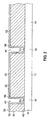
- FIG. 1 One process for forming an inductor according to the present invention begins as shown in Figure 1 , illustrating an integrated circuit semiconductor substrate 10, which conventionally includes a plurality of active elements (not shown). According to one embodiment of the present invention, to accommodate the inductor no active elements are formed within regions 12 and 14.
- a dielectric layer 40 (typically 3-5 microns thick) is formed over an upper surface 42 of the silicon substrate 10, followed by formation of windows 44 extending through the dielectric layer 40 to active elements in regions 46 and 48 of the substrate 10.
- the windows 44 are formed using known photolithographic masking, patterning and etching processes.
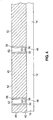
- a conductive material layer is formed overlying an upper surface 45.
- an inductor is formed in the conductive material layer, and interconnecting elements (e.g., tungsten plugs) are formed in the windows 44 for connecting the inductor to the active elements in the regions 46 and 48.
- a titanium layer 50 is deposited in the windows 44 and on a field region 52, i.e., an upper surface of the dielectric layer 40.
- the titanium layer 50 reacts with the underlying silicon of the active regions to form a localized titanium silicide region.
- This silicide region provides improved conductivity between the active regions and the interconnecting tungsten plugs formed later in the windows 44.
- TiN layer 58 is deposited within the windows 44 and on the field region 52. It is known that titanium-nitride can delaminate from oxide-based materials such as the dielectric layer 40.
- the titanium layer 50 serves as an adhesion layer to promote bonding between the titanium-nitride layer 58 and the underlying dielectric material of the field region 52, sidewalls 56 and bottom surfaces 53.
- the TiN layer 58 serves as a barrier between the underlying titanium layer and the fluorine-based gas used during the tungsten deposition step described below, as the fluorine-based gas is highly reactive with titanium.
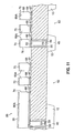
- a tungsten layer 60 is formed in the windows 44 and in the field region 52 by a chemical vapor deposition process involving tungsten hexafluoride (WF 6 ) and silane (SiH 4 ).
- the silicon substrate 10 then undergoes a chemical-mechanical polishing step, forming tungsten plugs 62. See Figure 4 .
- an aluminum stack 66 comprising, from bottom to top, a titanium layer 67, a titanium nitride layer 68, an aluminum layer 69 and an anti-reflective cap layer 70, is deposited over the field region 52.
- the titanium layer 67 and the titanium-nitride layer 68 of the aluminum stack 66 serve the same purposes as the titanium and titanium nitride layers 50 and 58 described above.
- Certain regions of the aluminum stack 66 are removed using conventional masking, patterning and etching steps, to form, in one region of the substrate 10, the desired conductor shape for an inductor 71, comprising a plurality of aluminum conductive lines 66A as shown in Figure 6 .
- conductive interconnect structures are formed in the aluminum stack 66 by masking, patterning and etching steps, and underlying conductive tungsten plugs are formed in contact with active regions in the substrate 10.
- the interconnect structures referred to as a metal-1 layer or first metallization layer, connect to the underlying tungsten plugs.
- additional interconnect structures, conductive vias and intermetallic dielectric layers are formed overlying the aluminum stack 66 to form a complete interconnect system for the integrated circuit.
- formation of the inductor 71 is conveniently integrated into the process for forming device interconnects, as the inductor can be formed simultaneously with formation of the interconnect structures.
- the conductive lines 66A are linear and intersect at about a 90° angle, forming a linear spiral-shaped inductor 71. Terminal ends 76 of the inductor 71 may be connected to underlying active devices in the regions 46 and 48 by the tungsten plugs 62.
- a curved spiral inductor 80 as shown in Figure 8 can also be formed by appropriate masking, patterning and etching of material regions of the aluminum stack 66.
- An inductor having a desired inductance value can be formed by appropriate selection of the size and geometrical pattern of the conductors forming the inductor 71.
- the inductor 71 is formed in a metal-1 layer or a first metallization layer. In other embodiments illustrated below, the inductor is formed in upper level metallization layers.
- the regions 12 and 14 of the substrate 10 underlying the inductor 71 are removed after formation of the inductor 71, forming voids 82.
- the resulting structure is illustrated in the cross-sectional view of Figure 9 and the plan view of Figure 10 .
- Material etching processes or laser micro-machining are known techniques that can be employed to remove the regions 12 and 14, which are typically about 300-500 microns thick.
- the voids 82 have a rectangular shape in Figure 10 , this is merely exemplary.
- the void for a circular spiral inductor, for example, would typically be circular.
- the voids 82 can be filled with a non-conductive, dielectric or packaging material such as epoxy or polyimide.
- the voids 82 are formed in the substrate 10 prior to formation of the inductor 71, although such a technique may be more difficult as it may be necessary to fill the void with a dielectric material, such as silicon dioxide, to allow subsequent formation of overlying layers.
- the absence of semiconductor and conductive material below the inductor 71 lowers inductor-induced eddy currents and raises the inductor Q factor.
- Figure 11 illustrates an embodiment of an inductor 89 comprising a conductive element 90 in the same metallization layer as the conductive lines 66A,for extending the terminal end 76.
- the void 82 is larger than in the embodiment of Figure 9 , thus increasing the Q factor of the inductor 89, when compared with the inductor 71 of Figure 9 .
- Figure 12 is a plan view of the inductor 89 of Figure 11 , with the cross-sectional view of Figure 11 taken along the plane 11-11 of Figure 12 .
- Figure 13 is a cross-sectional view of an inductor 92, wherein both terminal ends 76 are spaced apart from the inductor 71 to allow the formation of a larger void 82 than present in the embodiments described heretofore.
- an intermetallic dielectric layer 94 is disposed over the conductive lines 66A, and a second metallization layer overlying the intermetallic dielectric layer 94 comprises a conductive element 98 formed therein.
- a tungsten plug 100 connects the terminal end 76 to the conductive element 98.
- a tungsten plug 102 connects the conductive line 98 to an active region in the substrate 10. With both terminal ends 76 connected to an active region outside the footprint of the inductor 92, the void 82 can encompass substantially the entire region below the inductor 92.
- an integrated circuit generally comprises a plurality of metallization layers for interconnecting device active regions formed within the semiconductor substrate. These layers are typically referred to with a numerical indicator preceded by the letter "M,” for metallization, such as metallization layer one (M1).
- M1 metallization layer one
- an inductor is formed in an upper metallization layer (i.e., above M1), with upwardly and/or downwardly extending tungsten plugs for connecting inductor terminal ends to device active regions or other conductive structures.
- a fifth metallization layer is about 5 microns from the semiconductor substrate 10.
- An inductor formed therein is therefore about 5 microns from the substrate 10. It has been observed that removal of underlying substrate material (according to the teachings of the present invention) with a 5 micron separation between the inductor and the substrate improves the inductor Q.
- the known lossy substrate effects discussed above are observed up to an inductor-substrate separation distance equal to at least the diameter of the inductor. Typical inductor diameters may be in the range of 50-100 microns.
- teachings of the present invention may be advantageously employed where the inductor is formed in any of the metallization layers, since all the metallization layers are within 100 microns of the semiconductor substrate.
- Figure 14 is a cross-sectional view illustrating an embodiment of the present invention wherein an inductor 120 is formed in the third metallization layer or M3 of an integrated circuit device.
- Figure 14 does not illustrate certain ancillary layers (e.g., titanium and titanium-nitride) shown in the embodiments above.
- a semiconductor substrate 122 comprises a plurality of active devices (not shown) formed according to known prior art techniques.
- Conductive vias 124 are formed in a dielectric layer 126.
- a first metallization layer (M1) comprises conductive structures 128 for interconnecting the conductive vias 124 to overlying conductive vias 130 formed in an intermetallic dielectric layer 132. As is known in the art, the conductive structures also extend into and outwardly from the plane of the Figure 14 cross-section.
- a second metallization layer (M2) comprises conductive structures 140 overlying the conductive vias 130 and connected to conductive vias 142 formed in an intermetallic dielectric layer 144.
- the third metallization layer comprises the inductor 120 and a conductive structure 146, which are formed simultaneously by known masking, patterning and etching steps performed on a conductive layer formed overlying the intermetallic dielectric later 144. Additional metallization layers and intermetallic dielectric layers (not shown in Figure 14 ) can be formed over the illustrated structure.
- voids Prior to formation of the intermetallic dielectric layer 144 voids are formed in regions 150, underlying the inductor 120, using conventional masking, patterning and etching steps.
- the voids can be filled with silicon dioxide (a dielectric material) or another relatively low loss material prior to formation of the intermetallic dielectric layer 144 thereover.
- a region of the substrate 122 below the inductor 120 is also removed, according to the teachings above. As in the previous embodiment, the absence of semiconductor and metallization layers below the inductor 120 reduces eddy current loses and improves the inductor Q factor.
Landscapes
- Engineering & Computer Science (AREA)
- Power Engineering (AREA)
- Microelectronics & Electronic Packaging (AREA)
- Manufacturing & Machinery (AREA)
- Semiconductor Integrated Circuits (AREA)
- Coils Or Transformers For Communication (AREA)
- Internal Circuitry In Semiconductor Integrated Circuit Devices (AREA)
Priority Applications (1)
| Application Number | Priority Date | Filing Date | Title |
|---|---|---|---|
| EP07075479.1A EP1830402B1 (en) | 2003-08-22 | 2004-08-20 | A spiral inductor formed in a semiconductor substrate and a method for forming the inductor |
Applications Claiming Priority (2)
| Application Number | Priority Date | Filing Date | Title |
|---|---|---|---|
| US10/646,997 US7075167B2 (en) | 2003-08-22 | 2003-08-22 | Spiral inductor formed in a semiconductor substrate |
| US646997 | 2003-08-22 |
Related Child Applications (2)
| Application Number | Title | Priority Date | Filing Date |
|---|---|---|---|
| EP07075479.1A Division EP1830402B1 (en) | 2003-08-22 | 2004-08-20 | A spiral inductor formed in a semiconductor substrate and a method for forming the inductor |
| EP07075479.1A Division-Into EP1830402B1 (en) | 2003-08-22 | 2004-08-20 | A spiral inductor formed in a semiconductor substrate and a method for forming the inductor |
Publications (3)
| Publication Number | Publication Date |
|---|---|
| EP1513170A2 EP1513170A2 (en) | 2005-03-09 |
| EP1513170A3 EP1513170A3 (en) | 2005-05-25 |
| EP1513170B1 true EP1513170B1 (en) | 2014-09-24 |
Family
ID=34136607
Family Applications (2)
| Application Number | Title | Priority Date | Filing Date |
|---|---|---|---|
| EP04255018.6A Expired - Lifetime EP1513170B1 (en) | 2003-08-22 | 2004-08-20 | A spiral inductor formed in a semiconductor substrate and a method for forming the inductor |
| EP07075479.1A Expired - Lifetime EP1830402B1 (en) | 2003-08-22 | 2004-08-20 | A spiral inductor formed in a semiconductor substrate and a method for forming the inductor |
Family Applications After (1)
| Application Number | Title | Priority Date | Filing Date |
|---|---|---|---|
| EP07075479.1A Expired - Lifetime EP1830402B1 (en) | 2003-08-22 | 2004-08-20 | A spiral inductor formed in a semiconductor substrate and a method for forming the inductor |
Country Status (7)
| Country | Link |
|---|---|
| US (2) | US7075167B2 (https=) |
| EP (2) | EP1513170B1 (https=) |
| JP (2) | JP2005072588A (https=) |
| KR (1) | KR101084959B1 (https=) |
| CN (3) | CN101345242B (https=) |
| SG (1) | SG109577A1 (https=) |
| TW (2) | TWI412119B (https=) |
Cited By (1)
| Publication number | Priority date | Publication date | Assignee | Title |
|---|---|---|---|---|
| CN106169470A (zh) * | 2015-05-22 | 2016-11-30 | 飞思卡尔半导体公司 | 具有形成于空腔之上的导电特征的装置及其对应的方法 |
Families Citing this family (24)
| Publication number | Priority date | Publication date | Assignee | Title |
|---|---|---|---|---|
| US7075167B2 (en) * | 2003-08-22 | 2006-07-11 | Agere Systems Inc. | Spiral inductor formed in a semiconductor substrate |
| US7205632B2 (en) * | 2004-04-05 | 2007-04-17 | Taiwan Semiconductor Manufacturing Company, Ltd. | Anti-scattering attenuator structure for high energy particle radiation into integrated circuits |
| US7215000B2 (en) * | 2004-08-23 | 2007-05-08 | Texas Instruments Incorporated | Selectively encased surface metal structures in a semiconductor device |
| JP2007049115A (ja) * | 2005-07-13 | 2007-02-22 | Seiko Epson Corp | 半導体装置 |
| GB2440365A (en) * | 2006-07-21 | 2008-01-30 | X Fab Uk Ltd | A semiconductor device |
| US7935607B2 (en) * | 2007-04-09 | 2011-05-03 | Freescale Semiconductor, Inc. | Integrated passive device with a high resistivity substrate and method for forming the same |
| KR100947933B1 (ko) * | 2007-08-28 | 2010-03-15 | 주식회사 동부하이텍 | 인덕터 및 그 제조 방법 |
| CN101442048B (zh) * | 2007-11-23 | 2010-09-08 | 上海华虹Nec电子有限公司 | 射频cmos集成电感中的接地环结构 |
| CN101924102B (zh) * | 2009-06-15 | 2013-07-31 | 慧国(上海)软件科技有限公司 | 半导体装置 |
| JP2011040882A (ja) * | 2009-08-07 | 2011-02-24 | Sony Corp | 高周波デバイス |
| JP2011049397A (ja) * | 2009-08-27 | 2011-03-10 | Sony Corp | 高周波デバイス |
| TWI412114B (zh) * | 2009-12-31 | 2013-10-11 | 日月光半導體製造股份有限公司 | 半導體封裝結構及其製造方法 |
| TWI436463B (zh) * | 2009-12-31 | 2014-05-01 | 日月光半導體製造股份有限公司 | 半導體封裝結構及其製造方法 |
| US8710622B2 (en) * | 2011-11-17 | 2014-04-29 | Harris Corporation | Defected ground plane inductor |
| US8580647B2 (en) * | 2011-12-19 | 2013-11-12 | Taiwan Semiconductor Manufacturing Company, Ltd. | Inductors with through VIAS |
| CN105609267B (zh) * | 2014-11-14 | 2018-08-07 | 乾坤科技股份有限公司 | 无基板电子组件及其制造方法 |
| US9484297B2 (en) | 2015-03-13 | 2016-11-01 | Globalfoundries Inc. | Semiconductor device having non-magnetic single core inductor and method of producing the same |
| US10075132B2 (en) | 2015-03-24 | 2018-09-11 | Nxp Usa, Inc. | RF amplifier with conductor-less region underlying filter circuit inductor, and methods of manufacture thereof |
| US9509251B2 (en) | 2015-03-24 | 2016-11-29 | Freescale Semiconductor, Inc. | RF amplifier module and methods of manufacture thereof |
| US9787254B2 (en) | 2015-09-23 | 2017-10-10 | Nxp Usa, Inc. | Encapsulated semiconductor device package with heatsink opening, and methods of manufacture thereof |
| US11373803B2 (en) * | 2017-08-11 | 2022-06-28 | Applied Materials, Inc. | Method of forming a magnetic core on a substrate |
| US10672704B2 (en) * | 2017-11-30 | 2020-06-02 | Taiwan Semiconductor Manufacturing Company Ltd. | Semiconductor device with polygonal inductive device |
| CN108133101B (zh) * | 2017-12-21 | 2021-09-24 | 上海华力微电子有限公司 | 一种电感版图之辅助层及器件参数抽取的方法 |
| US10535635B2 (en) | 2018-06-15 | 2020-01-14 | Taiwan Semiconductor Manufacturing Company, Ltd. | Second semiconductor wafer attached to a first semiconductor wafer with a through hole connected to an inductor |
Family Cites Families (35)
| Publication number | Priority date | Publication date | Assignee | Title |
|---|---|---|---|---|
| US5227659A (en) | 1990-06-08 | 1993-07-13 | Trustees Of Boston University | Integrated circuit inductor |
| JPH0677407A (ja) * | 1992-04-06 | 1994-03-18 | Nippon Precision Circuits Kk | 半導体装置 |
| WO1994007348A1 (en) * | 1992-09-24 | 1994-03-31 | Hughes Aircraft Company | Dielectric vias within multilayer 3-dimensional structures/substrates |
| WO1994017558A1 (en) * | 1993-01-29 | 1994-08-04 | The Regents Of The University Of California | Monolithic passive component |
| US5370766A (en) | 1993-08-16 | 1994-12-06 | California Micro Devices | Methods for fabrication of thin film inductors, inductor networks and integration with other passive and active devices |
| US5446311A (en) | 1994-09-16 | 1995-08-29 | International Business Machines Corporation | High-Q inductors in silicon technology without expensive metalization |
| JP2904086B2 (ja) * | 1995-12-27 | 1999-06-14 | 日本電気株式会社 | 半導体装置およびその製造方法 |
| US6492705B1 (en) | 1996-06-04 | 2002-12-10 | Intersil Corporation | Integrated circuit air bridge structures and methods of fabricating same |
| US5736749A (en) | 1996-11-19 | 1998-04-07 | Lucent Technologies Inc. | Integrated circuit device with inductor incorporated therein |
| TW327253B (en) * | 1997-05-23 | 1998-02-21 | Vanguard Int Semiconduct Corp | The manufacturing method of metallization for IC |
| US6160303A (en) | 1997-08-29 | 2000-12-12 | Texas Instruments Incorporated | Monolithic inductor with guard rings |
| US6153489A (en) * | 1997-12-22 | 2000-11-28 | Electronics And Telecommunications Research Institute | Fabrication method of inductor devices using a substrate conversion technique |
| TW363278B (en) | 1998-01-16 | 1999-07-01 | Winbond Electronics Corp | Preparation method for semiconductor to increase the inductive resonance frequency and Q value |
| TW367623B (en) * | 1998-02-20 | 1999-08-21 | Winbond Electronic Corp | High Q value inductor and forming method thereof |
| US6025261A (en) * | 1998-04-29 | 2000-02-15 | Micron Technology, Inc. | Method for making high-Q inductive elements |
| JPH11354330A (ja) | 1998-06-08 | 1999-12-24 | Mitsubishi Materials Corp | 積層チップ部品およびその使用方法 |
| US6426267B2 (en) * | 1998-06-19 | 2002-07-30 | Winbond Electronics Corp. | Method for fabricating high-Q inductance device in monolithic technology |
| JP2000022085A (ja) * | 1998-06-29 | 2000-01-21 | Toshiba Corp | 半導体装置及びその製造方法 |
| US6249191B1 (en) | 1998-11-23 | 2001-06-19 | Micron Technology, Inc. | Monolithic integrated circuit oscillators, complementary metal oxide semiconductor (CMOS) voltage-controlled oscillators, integrated circuit oscillators, oscillator-forming methods, and oscillation methods |
| US6083802A (en) | 1998-12-31 | 2000-07-04 | Winbond Electronics Corporation | Method for forming an inductor |
| US6310387B1 (en) * | 1999-05-03 | 2001-10-30 | Silicon Wave, Inc. | Integrated circuit inductor with high self-resonance frequency |
| US6140197A (en) | 1999-08-30 | 2000-10-31 | Chartered Semiconductor Manufacturing Ltd. | Method of making spiral-type RF inductors having a high quality factor (Q) |
| JP2001168288A (ja) * | 1999-12-13 | 2001-06-22 | Seiko Epson Corp | 半導体装置 |
| US6503838B1 (en) * | 1999-12-31 | 2003-01-07 | Texas Instruments Incorporated | Integrated circuit isolation of functionally distinct RF circuits |
| JP2001223331A (ja) * | 2000-02-07 | 2001-08-17 | Sony Corp | 半導体装置及びその製造方法 |
| US6800533B1 (en) | 2000-03-06 | 2004-10-05 | Chartered Semiconductor Manufacturing Ltd. | Integrated vertical spiral inductor on semiconductor material |
| JP2002009299A (ja) * | 2000-04-17 | 2002-01-11 | Mitsubishi Electric Corp | 半導体装置の製造方法 |
| US6429504B1 (en) * | 2000-05-16 | 2002-08-06 | Tyco Electronics Corporation | Multilayer spiral inductor and integrated circuits incorporating the same |
| US6420773B1 (en) | 2000-10-04 | 2002-07-16 | Winbond Electronics Corp. | Multi-level spiral inductor structure having high inductance (L) and high quality factor (Q) |
| JP2002164512A (ja) * | 2000-11-28 | 2002-06-07 | Fujitsu Ltd | 半導体装置及びその製造方法 |
| US6534843B2 (en) | 2001-02-10 | 2003-03-18 | International Business Machines Corporation | High Q inductor with faraday shield and dielectric well buried in substrate |
| US6712983B2 (en) * | 2001-04-12 | 2004-03-30 | Memsic, Inc. | Method of etching a deep trench in a substrate and method of fabricating on-chip devices and micro-machined structures using the same |
| JP3666411B2 (ja) * | 2001-05-07 | 2005-06-29 | ソニー株式会社 | 高周波モジュール装置 |
| JP4355128B2 (ja) * | 2002-07-04 | 2009-10-28 | 富士通マイクロエレクトロニクス株式会社 | 半導体装置およびその製造方法 |
| US7075167B2 (en) | 2003-08-22 | 2006-07-11 | Agere Systems Inc. | Spiral inductor formed in a semiconductor substrate |
-
2003
- 2003-08-22 US US10/646,997 patent/US7075167B2/en not_active Expired - Lifetime
-
2004
- 2004-06-29 TW TW093119217A patent/TWI412119B/zh not_active IP Right Cessation
- 2004-06-29 TW TW102102447A patent/TWI418017B/zh not_active IP Right Cessation
- 2004-08-04 CN CN200810210288XA patent/CN101345242B/zh not_active Expired - Lifetime
- 2004-08-04 CN CN2004100558476A patent/CN1707806B/zh not_active Expired - Lifetime
- 2004-08-04 CN CN201010115825XA patent/CN101794775B/zh not_active Expired - Lifetime
- 2004-08-18 SG SG200404702A patent/SG109577A1/en unknown
- 2004-08-20 KR KR1020040065903A patent/KR101084959B1/ko not_active Expired - Lifetime
- 2004-08-20 EP EP04255018.6A patent/EP1513170B1/en not_active Expired - Lifetime
- 2004-08-20 EP EP07075479.1A patent/EP1830402B1/en not_active Expired - Lifetime
- 2004-08-20 JP JP2004240186A patent/JP2005072588A/ja active Pending
-
2006
- 2006-05-19 US US11/419,252 patent/US7381607B2/en not_active Expired - Lifetime
-
2007
- 2007-08-13 JP JP2007210590A patent/JP2007300143A/ja active Pending
Cited By (3)
| Publication number | Priority date | Publication date | Assignee | Title |
|---|---|---|---|---|
| CN106169470A (zh) * | 2015-05-22 | 2016-11-30 | 飞思卡尔半导体公司 | 具有形成于空腔之上的导电特征的装置及其对应的方法 |
| US9871107B2 (en) | 2015-05-22 | 2018-01-16 | Nxp Usa, Inc. | Device with a conductive feature formed over a cavity and method therefor |
| CN106169470B (zh) * | 2015-05-22 | 2021-11-09 | 恩智浦美国有限公司 | 具有形成于空腔之上的导电特征的装置及其对应的方法 |
Also Published As
| Publication number | Publication date |
|---|---|
| CN1707806B (zh) | 2010-08-18 |
| TWI412119B (zh) | 2013-10-11 |
| CN101345242A (zh) | 2009-01-14 |
| JP2005072588A (ja) | 2005-03-17 |
| US20050040471A1 (en) | 2005-02-24 |
| CN101345242B (zh) | 2010-07-21 |
| TW201330228A (zh) | 2013-07-16 |
| SG109577A1 (en) | 2005-03-30 |
| US7075167B2 (en) | 2006-07-11 |
| CN1707806A (zh) | 2005-12-14 |
| CN101794775A (zh) | 2010-08-04 |
| EP1830402B1 (en) | 2015-06-17 |
| JP2007300143A (ja) | 2007-11-15 |
| KR20050020707A (ko) | 2005-03-04 |
| EP1830402A2 (en) | 2007-09-05 |
| US7381607B2 (en) | 2008-06-03 |
| KR101084959B1 (ko) | 2011-11-23 |
| EP1830402A3 (en) | 2007-10-17 |
| CN101794775B (zh) | 2011-12-28 |
| EP1513170A3 (en) | 2005-05-25 |
| US20070107206A1 (en) | 2007-05-17 |
| TWI418017B (zh) | 2013-12-01 |
| TW200509370A (en) | 2005-03-01 |
| EP1513170A2 (en) | 2005-03-09 |
Similar Documents
| Publication | Publication Date | Title |
|---|---|---|
| EP1513170B1 (en) | A spiral inductor formed in a semiconductor substrate and a method for forming the inductor | |
| JP4948756B2 (ja) | 集積回路内に形成されたインダクタ及びその製造方法 | |
| US7969274B2 (en) | Method to improve inductance with a high-permeability slotted plate core in an integrated circuit | |
| US6903644B2 (en) | Inductor device having improved quality factor | |
| EP1352403B1 (en) | Integrated transformer | |
| US7791447B2 (en) | Integrated transformer | |
| JP4584533B2 (ja) | 半導体基板中に形成された薄膜多層高qトランスフォーマ | |
| US8004061B1 (en) | Conductive trace with reduced RF impedance resulting from the skin effect |
Legal Events
| Date | Code | Title | Description |
|---|---|---|---|
| PUAI | Public reference made under article 153(3) epc to a published international application that has entered the european phase |
Free format text: ORIGINAL CODE: 0009012 |
|
| AK | Designated contracting states |
Kind code of ref document: A2 Designated state(s): AT BE BG CH CY CZ DE DK EE ES FI FR GB GR HU IE IT LI LU MC NL PL PT RO SE SI SK TR |
|
| AX | Request for extension of the european patent |
Extension state: AL HR LT LV MK |
|
| PUAL | Search report despatched |
Free format text: ORIGINAL CODE: 0009013 |
|
| AK | Designated contracting states |
Kind code of ref document: A3 Designated state(s): AT BE BG CH CY CZ DE DK EE ES FI FR GB GR HU IE IT LI LU MC NL PL PT RO SE SI SK TR |
|
| AX | Request for extension of the european patent |
Extension state: AL HR LT LV MK |
|
| 17P | Request for examination filed |
Effective date: 20051123 |
|
| AKX | Designation fees paid |
Designated state(s): FR GB |
|
| REG | Reference to a national code |
Ref country code: DE Ref legal event code: 8566 |
|
| 17Q | First examination report despatched |
Effective date: 20061214 |
|
| RIC1 | Information provided on ipc code assigned before grant |
Ipc: H01F 41/04 20060101ALI20130909BHEP Ipc: H01L 23/522 20060101AFI20130909BHEP Ipc: H01L 27/08 20060101ALI20130909BHEP Ipc: H01F 17/00 20060101ALI20130909BHEP Ipc: H01L 49/02 20060101ALI20130909BHEP |
|
| GRAP | Despatch of communication of intention to grant a patent |
Free format text: ORIGINAL CODE: EPIDOSNIGR1 |
|
| INTG | Intention to grant announced |
Effective date: 20140109 |
|
| RAP1 | Party data changed (applicant data changed or rights of an application transferred) |
Owner name: AGERE SYSTEMS, INC. |
|
| GRAS | Grant fee paid |
Free format text: ORIGINAL CODE: EPIDOSNIGR3 |
|
| GRAP | Despatch of communication of intention to grant a patent |
Free format text: ORIGINAL CODE: EPIDOSNIGR1 |
|
| INTG | Intention to grant announced |
Effective date: 20140701 |
|
| GRAA | (expected) grant |
Free format text: ORIGINAL CODE: 0009210 |
|
| AK | Designated contracting states |
Kind code of ref document: B1 Designated state(s): FR GB |
|
| REG | Reference to a national code |
Ref country code: GB Ref legal event code: FG4D |
|
| PLBE | No opposition filed within time limit |
Free format text: ORIGINAL CODE: 0009261 |
|
| STAA | Information on the status of an ep patent application or granted ep patent |
Free format text: STATUS: NO OPPOSITION FILED WITHIN TIME LIMIT |
|
| 26N | No opposition filed |
Effective date: 20150625 |
|
| GBPC | Gb: european patent ceased through non-payment of renewal fee |
Effective date: 20150820 |
|
| REG | Reference to a national code |
Ref country code: FR Ref legal event code: ST Effective date: 20160429 |
|
| PG25 | Lapsed in a contracting state [announced via postgrant information from national office to epo] |
Ref country code: GB Free format text: LAPSE BECAUSE OF NON-PAYMENT OF DUE FEES Effective date: 20150820 |
|
| PG25 | Lapsed in a contracting state [announced via postgrant information from national office to epo] |
Ref country code: FR Free format text: LAPSE BECAUSE OF NON-PAYMENT OF DUE FEES Effective date: 20150831 |