EP1473736A2 - Nichtflüchtige ferroelektrische Speicheranordnung - Google Patents
Nichtflüchtige ferroelektrische Speicheranordnung Download PDFInfo
- Publication number
- EP1473736A2 EP1473736A2 EP04017770A EP04017770A EP1473736A2 EP 1473736 A2 EP1473736 A2 EP 1473736A2 EP 04017770 A EP04017770 A EP 04017770A EP 04017770 A EP04017770 A EP 04017770A EP 1473736 A2 EP1473736 A2 EP 1473736A2
- Authority
- EP
- European Patent Office
- Prior art keywords
- transistor
- gate electrode
- ferroelectric
- capacitors
- diffusion regions
- Prior art date
- Legal status (The legal status is an assumption and is not a legal conclusion. Google has not performed a legal analysis and makes no representation as to the accuracy of the status listed.)
- Withdrawn
Links
Images


Classifications
-
- G—PHYSICS
- G11—INFORMATION STORAGE
- G11C—STATIC STORES
- G11C11/00—Digital stores characterised by the use of particular electric or magnetic storage elements; Storage elements therefor
- G11C11/21—Digital stores characterised by the use of particular electric or magnetic storage elements; Storage elements therefor using electric elements
- G11C11/22—Digital stores characterised by the use of particular electric or magnetic storage elements; Storage elements therefor using electric elements using ferroelectric elements
- G11C11/223—Digital stores characterised by the use of particular electric or magnetic storage elements; Storage elements therefor using electric elements using ferroelectric elements using MOS with ferroelectric gate insulating film
-
- G—PHYSICS
- G11—INFORMATION STORAGE
- G11C—STATIC STORES
- G11C11/00—Digital stores characterised by the use of particular electric or magnetic storage elements; Storage elements therefor
- G11C11/21—Digital stores characterised by the use of particular electric or magnetic storage elements; Storage elements therefor using electric elements
- G11C11/22—Digital stores characterised by the use of particular electric or magnetic storage elements; Storage elements therefor using electric elements using ferroelectric elements
- G11C11/221—Digital stores characterised by the use of particular electric or magnetic storage elements; Storage elements therefor using electric elements using ferroelectric elements using ferroelectric capacitors
-
- G—PHYSICS
- G11—INFORMATION STORAGE
- G11C—STATIC STORES
- G11C11/00—Digital stores characterised by the use of particular electric or magnetic storage elements; Storage elements therefor
- G11C11/21—Digital stores characterised by the use of particular electric or magnetic storage elements; Storage elements therefor using electric elements
- G11C11/22—Digital stores characterised by the use of particular electric or magnetic storage elements; Storage elements therefor using electric elements using ferroelectric elements
- G11C11/225—Auxiliary circuits
- G11C11/2273—Reading or sensing circuits or methods
-
- G—PHYSICS
- G11—INFORMATION STORAGE
- G11C—STATIC STORES
- G11C11/00—Digital stores characterised by the use of particular electric or magnetic storage elements; Storage elements therefor
- G11C11/21—Digital stores characterised by the use of particular electric or magnetic storage elements; Storage elements therefor using electric elements
- G11C11/22—Digital stores characterised by the use of particular electric or magnetic storage elements; Storage elements therefor using electric elements using ferroelectric elements
- G11C11/225—Auxiliary circuits
- G11C11/2275—Writing or programming circuits or methods
-
- H—ELECTRICITY
- H10—SEMICONDUCTOR DEVICES; ELECTRIC SOLID-STATE DEVICES NOT OTHERWISE PROVIDED FOR
- H10B—ELECTRONIC MEMORY DEVICES
- H10B53/00—Ferroelectric RAM [FeRAM] devices comprising ferroelectric memory capacitors
Definitions
- the present invention relates to a ferroelectric non-volatile memory device and, more particularly, to a ferroelectric non-volatile memory device having a ferroelectric capacitor connected to the gate of a MOS (Metal Oxide Semiconductor) or MIS (Metal Insulator Semiconductor) field effect transistor.
- MOS Metal Oxide Semiconductor
- MIS Metal Insulator Semiconductor
- Forming a junction between a semiconductor and a ferroelectric is expected to create, depending on the polarization direction of the ferroelectric, a state in which electrons are induced to the semiconductor surface, or a state in which holes are induced.
- Attempts have already been made to manufacture non-volatile memory devices which hold memory contents even after power-off operation by using a ferroelectric for the gate insulator film of a MOS field effect transistor and making the two states correspond to "0" and "1".
- no practical devices have been realized yet. Devices with this structure are difficult to manufacture because of the following main reason. If a semiconductor and ferroelectric are joined to each other, an interface state is formed to capture electrons and holes. This stops flowing a necessary current through the source-drain path of a field effect transistor.
- an MFIS Metal or Conductor
- F Ferroelectric
- I Insulator
- S Semiconductor
- MFMIS structure a dielectric (paraelectric) film such as a silicon dioxid (SiO 2 ) film that hardly forms any interface state with a semiconductor is inserted between a ferroelectric film and a semiconductor substrate.
- a conductive layer is further sandwiched between a ferroelectric film and a dielectric film.
- the semiconductor substrate is made of Si
- the ferroelectric film is made of lead zirconate titanate (PZT: PbZr 1-x Ti x O 3 )
- the dielectric film is made of SiO 2 .
- the MFIS structure may be adopted as the structure of the gate electrode, but the MFMIS structure is adopted for these materials in order to prevent mutual diffusion of Pb atoms in the PZT film and Si atoms in the SiO 2 film.
- the relative dielectric constant of SiO 2 is 3.9.
- the relative dielectric constant of PZT takes a value ranging from 200 to 600 depending on the composition ratio of Zr and Ti, and is assumed to be 390 for descriptive convenience. In general, the thickness of the SiO 2 film is 1/10 that of the PZT film.
- the ferroelectric capacitor and the dielectric capacitor have a capacitance ratio of 10 : 1.
- the voltage applied to each capacitor is inversely proportional to the capacitance of the capacitor.
- the voltage applied to the ferroelectric capacitor is 1/10 that to the dielectric capacitor, i.e., 1/11 the total voltage.
- an MFS structure in which the PZT film is directly deposited on the Si substrate is formed, and the polarization of the film can be inverted at 5V.
- An MFMIS structure formed at the same film thickness requires a high voltage of 55V for polarization inversion.
- FIG. 9A The equivalent circuit of the MFMIS structure is shown in FIG. 9A.
- reference symbol C F denotes a ferroelectric capacitor
- C I a dielectric capacitor.
- the whole semiconductor is kept at the ground potential without considering the capacitance of the depletion layer of the semiconductor.
- the capacitance of the series-inserted dielectric capacitor is small, the magnitude of an inverse electric field comes close to the coercive electric field (electric field necessary for resetting the polarization to 0) of the ferroelectric, and the polarization retention time becomes very short.
- the short retention time may not be ignored not only in the MFIS and MFMIS structures but also in the MFS structure. Even if an interface with low trapping state density can be formed between a ferroelectric film and a semiconductor film, and a field effect transistor having a fine MFS gate structure can be manufactured, the ferroelectric capacitor and the capacitance of a depletion layer formed in the semiconductor surface form a series capacitor to pose almost the same problem as shown in FIG. 9B.
- a conventional non-volatile memory device using a ferroelectric for the gate insulator film of a MOS field effect transistor must adopt the MFIS or MFMIS structure so as not to form an interface state between a semiconductor substrate and the ferroelectric film.
- this type of structure increases the data write-in voltage and shortens the data retention time.
- a ferroelectric non-volatile memory device comprising a MOS or MIS cell transistor, and two ferroelectric capacitors which are connected to a gate electrode of the transistor and have substantially the same remanent polarization, wherein data is stored by polarizing ferroelectric thin films of the capacitors in opposite directions with respect to the gate electrode of the transistor, and a selector transistor is formed on one side of one capacitor.
- a ferroelectric non-volatile memory device comprising a MOS or MIS cell transistor, two ferroelectric capacitors each of which has one terminal connected to a gate electrode of the cell transistor and has substantially the same remanent polarization, and a selector transistor connected to the other terminal of one of the ferroelectric capacitors, wherein data is stored by polarizing ferroelectric thin films of the capacitors in opposite directions with respect to the gate electrode of the cell transistor.
- a memory cell structure is formed by connecting two ferroelectric capacitors having almost the same remanent polarization to the gate electrode of a MOS or MIS cell transistor. Data is stored in accordance with the polarization direction and remanent polarization of the ferroelectric thin film.
- the ferroelectric thin films of the capacitors are polarized in opposite directions with respect to the gate electrode of the cell transistor. Electric charges generated upon polarization of the ferroelectric thin film are not induced to the semiconductor surface of the channel region of the cell transistor.
- the data write-in voltage can be decreased. Since the internal electric fields of the two ferroelectric capacitors are 0 regardless of whether data is held in a "0" or "1" state, the data retention time can be prolonged. That is, in a memory cell structure using the ferroelectric capacitors, the data write-in voltage can be decreased, and the data retention time can be prolonged.
- the selector transistor is connected to a side of one ferroelectric capacitor opposite to the cell transistor, an unselected cell can be prevented from being influenced by the write-in voltage.
- FIGS. 1A and 1B There will now be described a ferroelectric non-volatile memory device referring to FIGS. 1A and 1B.
- one terminal of each of two ferroelectric capacitors C A and C B having the same remanent polarization is connected to the gate of a cell transistor (MOSFET) Tr having a MOS structure.
- MOSFET cell transistor
- the other terminal of the capacitor C A is connected to a terminal A, whereas the other terminal of the capacitor C B is connected to a terminal B.
- the transistor Tr and the capacitors C A and C B constitute one memory cell.
- the ferroelectric films of the capacitors C A and C B are made of PZT, and have the same area and film thickness.
- the memory cell of this structure can also be used for an analog memory device. However, for descriptive convenience, the operation will be described by exemplifying a case in which the memory cell is used for a digital memory device. Although not shown, memory cells are arranged in a matrix to form a memory array.
- the terminal B is grounded, and a positive or negative voltage is applied to the terminal A.
- 1/2 the voltage applied to the terminal A is applied to set the potential of the semiconductor to a floating state or an intermediate potential between two series-connected ferroelectric capacitors.
- the data retention time is expected to be as long as that of a general one-transistor/one-capacitor ferroelectric memory cell having a structure similar to the DRAM. Since the voltage is directly applied to the ferroelectric capacitor, the write-in voltage is expected to be low even with a high relative dielectric constant of the ferroelectric thin film.
- the terminal A is opened, the semiconductor substrate is grounded, and a positive voltage is applied to the terminal B.
- the polarization amount of the ferroelectric capacitor C B greatly changes, and the electric charges Q G of the gate electrode change from 0.
- P be the polarization amount of the ferroelectric thin film upon application of a positive voltage
- Q G (P r + P)S (S: the area of the ferroelectric capacitor, P r : the remanent polarization of the ferroelectric film).
- the source-drain path flows a current by inversion electrons.
- data can be read by applying a pulse voltage to the terminal B and measuring the drain current of the MOSFET at this time.
- the voltage is applied through the gate insulator film of the MOSFET, and the read-out voltage may rise.
- the terminal B is grounded, a positive or negative voltage is applied to the terminal A, and the ferroelectric thin films of the ferroelectric capacitors C A and C B are polarized in opposite directions with respect to the gate electrode.
- Data can be stored in accordance with the polarization direction and remanent polarization of the ferroelectric thin film without inducing electric charges generated upon polarization of the ferroelectric thin film to the channel region. Since the internal electric fields of the two ferroelectric capacitors C A and C B are 0 regardless of whether data is held in a "0" or "1" state, the data retention time can be prolonged. Since the voltage is directly applied to the ferroelectric thin film, the data write-in voltage can be decreased.
- FIG. 2A shows a circuit used for operation analysis
- FIG. 2B shows a change in drain current upon application of a read-out pulse.
- switches SW0, SW1, and SW2 While switches SW0, SW1, and SW2 are OFF, ON, and OFF, respectively, a positive or negative voltage is applied to a terminal n2 to store data "0" or "1".
- the switches SW0, SW1, and SW2 are respectively turned off, on, and on, thereby holding the memory state.
- the switches SW0, SW1, and SW2 are respectively turned on, off, and off, and a voltage is applied to a terminal n0 to read out data. From FIGS. 2A and 2B, data "0" or “1” can be easily read out by measuring the drain current.
- This embodiment adds, to the structure of FIGS. 1A and 1B, a selector transistor comprised of a MOSFET so as not to influence an unselected cell by the write-in voltage.
- the MOSFET serving as a switch for selective write operation is connected to the portion (FIG. 3A) of the terminal A (or terminal B) in FIGS. 1A and 1B, or at a portion (FIG. 3B) between the gate and one capacitor.
- the gate of a cell transistor Q1 is connected to the node of the capacitors C A and C B connected in series to each other.
- a selector transistor Q2 is connected between a capacitor C B and a terminal b.
- the terminals a, b and c are connected a driver DR.
- a selector transistor Q2 is between the gate of the cell transistor Q 1 and the capacitor C B .
- FIG. 3A is superior because two capacitors can be directly formed on the floating gate electrode of the cell transistor. This embodiment will examine an arrangement in which the structure of FIG. 3A is processed as a unit cell.
- a voltage applied to the terminal c turns on/off the selector transistor Q2 to control whether a voltage appearing between the terminals a and b is actually applied to the ferroelectric capacitors C A and C B . Accordingly, voltages at the terminals a , b , and c must be independently controlled from a peripheral circuit. Constituting this memory cell array requires at least three control lines a' , b' , and c' . If the lines b' and c' are parallel to each other, cells connected to them similarly operate, and do not play the role as a selector switch. Hence, the lines b' and c' must cross each other, and the three lines are arranged as shown in FIG. 4A or 4B. According to convention, the lines a' , b' , and c' will be referred to as a plate line (PL), bit line (BL), and word line (WL).
- PL plate line
- BL bit line
- WL word line
- one terminal of the capacitor C A is connected to the gate electrode of the cell transistor Q1, and the other terminal is connected to the plate line PL.
- One terminal of the capacitor C B is connected to the gate electrode of the cell transistor Q1, and the other terminal is connected to the bit line BL via the selector transistor Q2.
- the gate electrode of the selector transistor Q2 is connected to the word line WL.
- the connection is the same except that the plate line PL is parallel to the word line WL.
- Read operation will be explained.
- the terminal of one capacitor is opened, the polarization of the other capacitor is reversed, and a current flowing through the d-e path at this time is detected.
- a new current detection line may be arranged, which is not preferable for a high cell arrangement density.
- the terminal d is connected to one of the word line WL, bit line BL, and plate line PL, and the terminal e is grounded.
- SOI Si film on an insulator
- FIG. 5A in addition to the structure of FIG. 4A, the source of the cell transistor Q1 is grounded, and its drain is connected to the word line WL.
- FIG. 5B in addition to the structure of FIG. 4B, the source of the cell transistor Q1 is grounded, and its drain is connected to the bit line BL.
- FIG. 5C in addition to the structure of FIG. 4A, the source of the cell transistor Q1 is grounded, and its drain is connected to the bit line BL.
- FIG. 5D in addition to the structure of FIG. 4B, the source of the cell transistor Q1 is grounded, and its drain is connected to the word line WL.
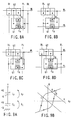
- FIG. 6 A structure in which the source of the cell transistor Q1 is grounded, and its drain is connected to the word line WL, like the connection of FIG. 5D, is shown in the sectional view of a device structure in FIG. 6.
- An n-channel MOS transistor (cell transistor) Q1 made up of n-type diffusion regions 62 and a gate electrode 63, and an n-channel MOS transistor (selector transistor) Q2 made up of n-type diffusion regions 64 and a gate electrode 65 are formed on a p-type Si substrate 61 so as to be adjacent to each other.
- Capacitor electrodes 67 and 68 are formed on the gate electrode 63 of the cell transistor Q1 via a ferroelectric film 66 and formed of ferroelectric thin films, thereby constituting the two ferroelectric capacitors C A and C B .
- FIGS. 7A to 7D If no common ground point exists, like an SOI substrate, a line grounded in read can be used. Connection methods in this case are shown in FIGS. 7A to 7D. In FIGS. 7A to 7D, some of the methods use the line of an adjacent cell in consideration of an actual arrangement.
- FIG. 7A unlike FIG. 5A, the source of the cell transistor Q1 is not grounded but is connected to a bit line BL2 of an adjacent cell parallel to a bit line BL1 connected to the selector transistor Q2.
- FIG. 7B unlike FIG. 5B, the source of the cell transistor Q1 is not grounded but is connected to the word line WL.
- FIG. 7C unlike FIG. 5C, the source of the cell transistor Q1 is not grounded but is connected to the word line WL.
- FIG. 7D unlike FIG. 5D, the source of the cell transistor Q1 is not grounded but is connected to the bit line BL2 of an adjacent cell parallel to the bit line BL1 connected to the selector transistor Q2.
- FIGS. 8A to 8D Examples of the cell arrangement in this case are shown in FIGS. 8A to 8D.
- FIGS. 8A to 8D correspond to FIGS. 7A to 7D, respectively.
- circuit arrangements as shown in FIGS. 7A to 7D can be laid out on the substrate without any change.
- the selector transistor Q2 is connected to the terminal of the ferroelectric capacitor C B opposite to the cell transistor, i.e., between the ferroelectric capacitor C B and the bit line BL.
- the data retention time can be prolonged, and the data write-in voltage can be decreased.
- an unselected cell can be prevented from being influenced by the write-in voltage.
- the reliability of the memory cell can be improved.
- the present invention is not limited to the above-described embodiment.
- This embodiment uses PZT as the ferroelectric material of the ferroelectric capacitor, but the ferroelectric material is not limited to this. Any ferroelectric material can be used.
- Two ferroelectric capacitors connected to the gate electrode of a MOS transistor may have different ferroelectric film thicknesses, but their material and area must be the same.
- the field effect transistor is not limited to a MOS transistor, and can be a MIS transistor using a gate insulator film instead of a gate oxide film.
- the Si stripe is not limited to an npn stripe, and may be a pnp stripe for formation of a p-channel transistor.
- a memory cell structure is formed by connecting two ferroelectric capacitors having almost the same remanent polarization to the gate electrode of a MOS or MIS field effect transistor.
- Data is stored by polarizing the ferroelectric thin films of the capacitors in opposite directions with respect to the gate electrode of the transistor. Since the voltage is directly applied to the ferroelectric thin film, the data write-in voltage can be decreased. At the same time, electric charges generated upon polarization of the ferroelectric thin film are not induced to the semiconductor surface of the channel region of the transistor. Since the internal electric fields of the two ferroelectric capacitors are 0 in a steady state after data is stored, the data retention time can be prolonged.
- the selector transistor is connected to one ferroelectric capacitor opposite to the cell transistor, an unselected cell can be prevented from being influenced by the write-in voltage.
Applications Claiming Priority (3)
| Application Number | Priority Date | Filing Date | Title |
|---|---|---|---|
| JP13851599A JP3377762B2 (ja) | 1999-05-19 | 1999-05-19 | 強誘電体不揮発性メモリ |
| JP13851599 | 1999-05-19 | ||
| EP00109433A EP1054406B1 (de) | 1999-05-19 | 2000-05-03 | Nichtflüchtige ferroelektrische Speicheranordnung |
Related Parent Applications (1)
| Application Number | Title | Priority Date | Filing Date |
|---|---|---|---|
| EP00109433A Division EP1054406B1 (de) | 1999-05-19 | 2000-05-03 | Nichtflüchtige ferroelektrische Speicheranordnung |
Publications (2)
| Publication Number | Publication Date |
|---|---|
| EP1473736A2 true EP1473736A2 (de) | 2004-11-03 |
| EP1473736A3 EP1473736A3 (de) | 2006-10-04 |
Family
ID=15223961
Family Applications (2)
| Application Number | Title | Priority Date | Filing Date |
|---|---|---|---|
| EP04017770A Withdrawn EP1473736A3 (de) | 1999-05-19 | 2000-05-03 | Nichtflüchtige ferroelektrische Speicheranordnung |
| EP00109433A Expired - Lifetime EP1054406B1 (de) | 1999-05-19 | 2000-05-03 | Nichtflüchtige ferroelektrische Speicheranordnung |
Family Applications After (1)
| Application Number | Title | Priority Date | Filing Date |
|---|---|---|---|
| EP00109433A Expired - Lifetime EP1054406B1 (de) | 1999-05-19 | 2000-05-03 | Nichtflüchtige ferroelektrische Speicheranordnung |
Country Status (6)
| Country | Link |
|---|---|
| US (2) | US6327172B1 (de) |
| EP (2) | EP1473736A3 (de) |
| JP (1) | JP3377762B2 (de) |
| KR (1) | KR100355779B1 (de) |
| DE (1) | DE60019191T2 (de) |
| TW (1) | TW454338B (de) |
Cited By (5)
| Publication number | Priority date | Publication date | Assignee | Title |
|---|---|---|---|---|
| DE102004011432A1 (de) * | 2004-03-09 | 2005-09-29 | Infineon Technologies Ag | Halbleiterspeicherzelle, Verfahren zu deren Herstellung und Halbleiterspeichereinrichtung |
| FR2904463A1 (fr) * | 2006-07-27 | 2008-02-01 | St Microelectronics Sa | Programmation d'un circuit de retention de charges pour mesure temporelle |
| WO2008012459A3 (fr) * | 2006-07-27 | 2008-03-13 | St Microelectronics Sa | Circuit de retention de charges pour mesure temporelle |
| US8036020B2 (en) | 2006-07-27 | 2011-10-11 | Stmicroelectronics S.A. | Circuit for reading a charge retention element for a time measurement |
| US8320176B2 (en) | 2006-07-27 | 2012-11-27 | Stmicroelectronics S.A. | EEPROM charge retention circuit for time measurement |
Families Citing this family (20)
| Publication number | Priority date | Publication date | Assignee | Title |
|---|---|---|---|---|
| DE10031947B4 (de) * | 2000-06-30 | 2006-06-14 | Infineon Technologies Ag | Schaltungsanordnung zum Ausgleich unterschiedlicher Spannungen auf Leitungszügen in integrierten Halbleiterschaltungen |
| US6720596B2 (en) | 2000-10-17 | 2004-04-13 | Matsushita Electric Industrial Co., Ltd. | Semiconductor device and method for driving the same |
| JP2002203913A (ja) * | 2000-12-28 | 2002-07-19 | Hitachi Ltd | 半導体記憶装置の製造方法および半導体記憶装置 |
| JP3522248B2 (ja) * | 2001-10-15 | 2004-04-26 | ローム株式会社 | 半導体集積回路装置 |
| JP3740577B2 (ja) * | 2001-12-20 | 2006-02-01 | 松下電器産業株式会社 | 負電位発生回路、負電位発生装置及びこれを用いた半導体装置 |
| JP2003209179A (ja) * | 2002-01-15 | 2003-07-25 | Fujitsu Ltd | 容量素子及びその製造方法 |
| JP2003263886A (ja) * | 2002-03-08 | 2003-09-19 | Fujitsu Ltd | ビット線容量を最適化できる強誘電体メモリ |
| KR100660901B1 (ko) * | 2005-12-22 | 2006-12-26 | 삼성전자주식회사 | 단일 게이트 구조를 갖는 이이피롬, 상기 이이피롬의동작방법 및 상기 이이피롬의 제조방법 |
| US7991041B2 (en) * | 2006-11-15 | 2011-08-02 | Qualcomm, Incorporated | Iterative detection and cancellation for wireless communication |
| US8781043B2 (en) * | 2006-11-15 | 2014-07-15 | Qualcomm Incorporated | Successive equalization and cancellation and successive mini multi-user detection for wireless communication |
| US7700985B2 (en) * | 2008-06-24 | 2010-04-20 | Seagate Technology Llc | Ferroelectric memory using multiferroics |
| WO2011063567A1 (en) | 2009-11-27 | 2011-06-03 | Qualcomm Incorporated | Interference cancellation for non-orthogonal channel sets |
| US8867256B2 (en) * | 2012-09-25 | 2014-10-21 | Palo Alto Research Center Incorporated | Systems and methods for writing and non-destructively reading ferroelectric memories |
| US20160005749A1 (en) * | 2014-07-01 | 2016-01-07 | Qualcomm Incorporated | Series ferroelectric negative capacitor for multiple time programmable (mtp) devices |
| US11088170B2 (en) | 2019-11-25 | 2021-08-10 | Sandisk Technologies Llc | Three-dimensional ferroelectric memory array including integrated gate selectors and methods of forming the same |
| US11335391B1 (en) | 2020-10-30 | 2022-05-17 | Ferroelectric Memory Gmbh | Memory cell arrangement and method thereof |
| US11527551B2 (en) * | 2020-10-30 | 2022-12-13 | Ferroelectric Memory Gmbh | Memory cell arrangements and methods thereof |
| US11380695B2 (en) | 2020-10-30 | 2022-07-05 | Ferroelectric Memory Gmbh | Memory cell arrangement and method thereof |
| WO2022094814A1 (zh) * | 2020-11-04 | 2022-05-12 | 华为技术有限公司 | 一种铁电存储器及存储设备 |
| US20230326923A1 (en) * | 2021-11-01 | 2023-10-12 | KYOCERA AVX Components Corporation | Combined MOS/MIS Capacitor Assembly |
Citations (3)
| Publication number | Priority date | Publication date | Assignee | Title |
|---|---|---|---|---|
| US5523964A (en) * | 1994-04-07 | 1996-06-04 | Symetrix Corporation | Ferroelectric non-volatile memory unit |
| US5856688A (en) * | 1997-05-09 | 1999-01-05 | Samsung Electronics Co., Ltd. | Integrated circuit memory devices having nonvolatile single transistor unit cells therein |
| US6046929A (en) * | 1998-04-06 | 2000-04-04 | Fujitsu Limited | Memory device with two ferroelectric capacitors per one cell |
Family Cites Families (9)
| Publication number | Priority date | Publication date | Assignee | Title |
|---|---|---|---|---|
| JP2788265B2 (ja) | 1988-07-08 | 1998-08-20 | オリンパス光学工業株式会社 | 強誘電体メモリ及びその駆動方法,製造方法 |
| JP3021614B2 (ja) | 1990-11-06 | 2000-03-15 | オリンパス光学工業株式会社 | メモリ素子 |
| JPH07122661A (ja) | 1993-10-27 | 1995-05-12 | Olympus Optical Co Ltd | 強誘電体メモリ装置 |
| WO1995026570A1 (fr) | 1994-03-29 | 1995-10-05 | Olympus Optical Co., Ltd. | Dispositif a memoire ferro-electrique |
| JPH08180673A (ja) | 1994-12-27 | 1996-07-12 | Nec Corp | 強誘電体メモリセル及びそのアクセス装置 |
| JPH1117123A (ja) | 1997-06-23 | 1999-01-22 | Rohm Co Ltd | 不揮発性記憶素子 |
| JPH1117112A (ja) | 1997-06-24 | 1999-01-22 | Oki Electric Ind Co Ltd | 半導体集積回路のチップレイアウト方法 |
| JP3495905B2 (ja) * | 1998-02-19 | 2004-02-09 | シャープ株式会社 | 半導体記憶装置 |
| US6198652B1 (en) * | 1998-04-13 | 2001-03-06 | Kabushiki Kaisha Toshiba | Non-volatile semiconductor integrated memory device |
-
1999
- 1999-05-19 JP JP13851599A patent/JP3377762B2/ja not_active Expired - Fee Related
-
2000
- 2000-05-03 DE DE60019191T patent/DE60019191T2/de not_active Withdrawn - After Issue
- 2000-05-03 EP EP04017770A patent/EP1473736A3/de not_active Withdrawn
- 2000-05-03 EP EP00109433A patent/EP1054406B1/de not_active Expired - Lifetime
- 2000-05-05 TW TW089108596A patent/TW454338B/zh not_active IP Right Cessation
- 2000-05-08 KR KR1020000024357A patent/KR100355779B1/ko not_active IP Right Cessation
- 2000-05-09 US US09/567,865 patent/US6327172B1/en not_active Expired - Fee Related
-
2001
- 2001-10-04 US US09/971,988 patent/US6584008B2/en not_active Expired - Fee Related
Patent Citations (3)
| Publication number | Priority date | Publication date | Assignee | Title |
|---|---|---|---|---|
| US5523964A (en) * | 1994-04-07 | 1996-06-04 | Symetrix Corporation | Ferroelectric non-volatile memory unit |
| US5856688A (en) * | 1997-05-09 | 1999-01-05 | Samsung Electronics Co., Ltd. | Integrated circuit memory devices having nonvolatile single transistor unit cells therein |
| US6046929A (en) * | 1998-04-06 | 2000-04-04 | Fujitsu Limited | Memory device with two ferroelectric capacitors per one cell |
Cited By (8)
| Publication number | Priority date | Publication date | Assignee | Title |
|---|---|---|---|---|
| DE102004011432A1 (de) * | 2004-03-09 | 2005-09-29 | Infineon Technologies Ag | Halbleiterspeicherzelle, Verfahren zu deren Herstellung und Halbleiterspeichereinrichtung |
| FR2904463A1 (fr) * | 2006-07-27 | 2008-02-01 | St Microelectronics Sa | Programmation d'un circuit de retention de charges pour mesure temporelle |
| WO2008012459A3 (fr) * | 2006-07-27 | 2008-03-13 | St Microelectronics Sa | Circuit de retention de charges pour mesure temporelle |
| WO2008012463A3 (fr) * | 2006-07-27 | 2008-04-03 | St Microelectronics Sa | Programmation d'un circuit de retention de charges pour mesure temporelle |
| US8036020B2 (en) | 2006-07-27 | 2011-10-11 | Stmicroelectronics S.A. | Circuit for reading a charge retention element for a time measurement |
| US8320176B2 (en) | 2006-07-27 | 2012-11-27 | Stmicroelectronics S.A. | EEPROM charge retention circuit for time measurement |
| US8331203B2 (en) | 2006-07-27 | 2012-12-11 | Stmicroelectronics S.A. | Charge retention circuit for a time measurement |
| US8339848B2 (en) | 2006-07-27 | 2012-12-25 | Stmicroelectronics S.A. | Programming of a charge retention circuit for a time measurement |
Also Published As
| Publication number | Publication date |
|---|---|
| EP1054406B1 (de) | 2005-04-06 |
| DE60019191D1 (de) | 2005-05-12 |
| DE60019191T2 (de) | 2006-03-09 |
| TW454338B (en) | 2001-09-11 |
| EP1054406A3 (de) | 2001-01-17 |
| KR100355779B1 (ko) | 2002-10-19 |
| KR20000077182A (ko) | 2000-12-26 |
| US20020012264A1 (en) | 2002-01-31 |
| US6327172B1 (en) | 2001-12-04 |
| JP3377762B2 (ja) | 2003-02-17 |
| EP1054406A2 (de) | 2000-11-22 |
| US6584008B2 (en) | 2003-06-24 |
| EP1473736A3 (de) | 2006-10-04 |
| JP2000331484A (ja) | 2000-11-30 |
Similar Documents
| Publication | Publication Date | Title |
|---|---|---|
| EP1054406B1 (de) | Nichtflüchtige ferroelektrische Speicheranordnung | |
| US6188600B1 (en) | Memory structure in ferroelectric nonvolatile memory and readout method therefor | |
| US5523964A (en) | Ferroelectric non-volatile memory unit | |
| EP0490240B1 (de) | Ferroelektrische Kondensator und Verfahren zum Herstellen von örtlichen Zwischenverbindungen | |
| US6714435B1 (en) | Ferroelectric transistor for storing two data bits | |
| US6898105B2 (en) | Ferroelectric non-volatile memory device having integral capacitor and gate electrode, and driving method of a ferroelectric non-volatile memory device | |
| US5877977A (en) | Nonvolatile memory based on metal-ferroelectric-metal-insulator semiconductor structure | |
| US6285577B1 (en) | Non-volatile memory using ferroelectric capacitor | |
| US7123503B2 (en) | Writing to ferroelectric memory devices | |
| WO2010097862A1 (ja) | 半導体メモリセル及びその製造方法並びに半導体記憶装置 | |
| US7167386B2 (en) | Ferroelectric memory and operating method therefor | |
| US6344991B1 (en) | Nonvolatile semiconductor memory device | |
| US6888736B2 (en) | Ferroelectric transistor for storing two data bits | |
| KR20030009073A (ko) | 반도체 기억장치 및 그 구동방법 | |
| JP3131340B2 (ja) | 強誘電体記憶素子 | |
| US6455883B2 (en) | Nonvolatile semiconductor memory | |
| Tsai et al. | Mechanism for slow switching effect in advanced low-voltage, high-speed Pb (Zr/sub 1-x/Ti/sub x/) O/sub 3/ferroelectric memory | |
| KR20000014807A (ko) | 이중 박막 트랜지스터 비파괴 읽기 강유전체 랜덤 액세스 메모리 및 그 작동방법 |
Legal Events
| Date | Code | Title | Description |
|---|---|---|---|
| PUAI | Public reference made under article 153(3) epc to a published international application that has entered the european phase |
Free format text: ORIGINAL CODE: 0009012 |
|
| 17P | Request for examination filed |
Effective date: 20040727 |
|
| AC | Divisional application: reference to earlier application |
Ref document number: 1054406 Country of ref document: EP Kind code of ref document: P |
|
| AK | Designated contracting states |
Kind code of ref document: A2 Designated state(s): DE FR |
|
| PUAL | Search report despatched |
Free format text: ORIGINAL CODE: 0009013 |
|
| AK | Designated contracting states |
Kind code of ref document: A3 Designated state(s): DE FR |
|
| RIC1 | Information provided on ipc code assigned before grant |
Ipc: G11C 27/02 20060101ALI20060828BHEP Ipc: G11C 11/22 20060101AFI20040908BHEP |
|
| 17Q | First examination report despatched |
Effective date: 20070514 |
|
| AKX | Designation fees paid |
Designated state(s): DE FR |
|
| GRAP | Despatch of communication of intention to grant a patent |
Free format text: ORIGINAL CODE: EPIDOSNIGR1 |
|
| STAA | Information on the status of an ep patent application or granted ep patent |
Free format text: STATUS: THE APPLICATION HAS BEEN WITHDRAWN |
|
| 18W | Application withdrawn |
Effective date: 20071213 |