EP1469448A1 - Procede de commande de la luminance d'un ecran electroluminescent organique et circuit de commande de luminance - Google Patents
Procede de commande de la luminance d'un ecran electroluminescent organique et circuit de commande de luminance Download PDFInfo
- Publication number
- EP1469448A1 EP1469448A1 EP02792039A EP02792039A EP1469448A1 EP 1469448 A1 EP1469448 A1 EP 1469448A1 EP 02792039 A EP02792039 A EP 02792039A EP 02792039 A EP02792039 A EP 02792039A EP 1469448 A1 EP1469448 A1 EP 1469448A1
- Authority
- EP
- European Patent Office
- Prior art keywords
- luminance
- reference voltage
- gain
- display
- organic electroluminescence
- Prior art date
- Legal status (The legal status is an assumption and is not a legal conclusion. Google has not performed a legal analysis and makes no representation as to the accuracy of the status listed.)
- Granted
Links
Images


Classifications
-
- G—PHYSICS
- G06—COMPUTING; CALCULATING OR COUNTING
- G06F—ELECTRIC DIGITAL DATA PROCESSING
- G06F3/00—Input arrangements for transferring data to be processed into a form capable of being handled by the computer; Output arrangements for transferring data from processing unit to output unit, e.g. interface arrangements
- G06F3/14—Digital output to display device ; Cooperation and interconnection of the display device with other functional units
- G06F3/147—Digital output to display device ; Cooperation and interconnection of the display device with other functional units using display panels
-
- G—PHYSICS
- G09—EDUCATION; CRYPTOGRAPHY; DISPLAY; ADVERTISING; SEALS
- G09G—ARRANGEMENTS OR CIRCUITS FOR CONTROL OF INDICATING DEVICES USING STATIC MEANS TO PRESENT VARIABLE INFORMATION
- G09G3/00—Control arrangements or circuits, of interest only in connection with visual indicators other than cathode-ray tubes
- G09G3/20—Control arrangements or circuits, of interest only in connection with visual indicators other than cathode-ray tubes for presentation of an assembly of a number of characters, e.g. a page, by composing the assembly by combination of individual elements arranged in a matrix no fixed position being assigned to or needed to be assigned to the individual characters or partial characters
- G09G3/22—Control arrangements or circuits, of interest only in connection with visual indicators other than cathode-ray tubes for presentation of an assembly of a number of characters, e.g. a page, by composing the assembly by combination of individual elements arranged in a matrix no fixed position being assigned to or needed to be assigned to the individual characters or partial characters using controlled light sources
- G09G3/30—Control arrangements or circuits, of interest only in connection with visual indicators other than cathode-ray tubes for presentation of an assembly of a number of characters, e.g. a page, by composing the assembly by combination of individual elements arranged in a matrix no fixed position being assigned to or needed to be assigned to the individual characters or partial characters using controlled light sources using electroluminescent panels
- G09G3/32—Control arrangements or circuits, of interest only in connection with visual indicators other than cathode-ray tubes for presentation of an assembly of a number of characters, e.g. a page, by composing the assembly by combination of individual elements arranged in a matrix no fixed position being assigned to or needed to be assigned to the individual characters or partial characters using controlled light sources using electroluminescent panels semiconductive, e.g. using light-emitting diodes [LED]
- G09G3/3208—Control arrangements or circuits, of interest only in connection with visual indicators other than cathode-ray tubes for presentation of an assembly of a number of characters, e.g. a page, by composing the assembly by combination of individual elements arranged in a matrix no fixed position being assigned to or needed to be assigned to the individual characters or partial characters using controlled light sources using electroluminescent panels semiconductive, e.g. using light-emitting diodes [LED] organic, e.g. using organic light-emitting diodes [OLED]
-
- G—PHYSICS
- G09—EDUCATION; CRYPTOGRAPHY; DISPLAY; ADVERTISING; SEALS
- G09G—ARRANGEMENTS OR CIRCUITS FOR CONTROL OF INDICATING DEVICES USING STATIC MEANS TO PRESENT VARIABLE INFORMATION
- G09G5/00—Control arrangements or circuits for visual indicators common to cathode-ray tube indicators and other visual indicators
- G09G5/02—Control arrangements or circuits for visual indicators common to cathode-ray tube indicators and other visual indicators characterised by the way in which colour is displayed
- G09G5/04—Control arrangements or circuits for visual indicators common to cathode-ray tube indicators and other visual indicators characterised by the way in which colour is displayed using circuits for interfacing with colour displays
-
- G—PHYSICS
- G09—EDUCATION; CRYPTOGRAPHY; DISPLAY; ADVERTISING; SEALS
- G09G—ARRANGEMENTS OR CIRCUITS FOR CONTROL OF INDICATING DEVICES USING STATIC MEANS TO PRESENT VARIABLE INFORMATION
- G09G2320/00—Control of display operating conditions
- G09G2320/02—Improving the quality of display appearance
- G09G2320/0238—Improving the black level
-
- G—PHYSICS
- G09—EDUCATION; CRYPTOGRAPHY; DISPLAY; ADVERTISING; SEALS
- G09G—ARRANGEMENTS OR CIRCUITS FOR CONTROL OF INDICATING DEVICES USING STATIC MEANS TO PRESENT VARIABLE INFORMATION
- G09G2320/00—Control of display operating conditions
- G09G2320/02—Improving the quality of display appearance
- G09G2320/0242—Compensation of deficiencies in the appearance of colours
-
- G—PHYSICS
- G09—EDUCATION; CRYPTOGRAPHY; DISPLAY; ADVERTISING; SEALS
- G09G—ARRANGEMENTS OR CIRCUITS FOR CONTROL OF INDICATING DEVICES USING STATIC MEANS TO PRESENT VARIABLE INFORMATION
- G09G2330/00—Aspects of power supply; Aspects of display protection and defect management
- G09G2330/02—Details of power systems and of start or stop of display operation
- G09G2330/021—Power management, e.g. power saving
-
- G—PHYSICS
- G09—EDUCATION; CRYPTOGRAPHY; DISPLAY; ADVERTISING; SEALS
- G09G—ARRANGEMENTS OR CIRCUITS FOR CONTROL OF INDICATING DEVICES USING STATIC MEANS TO PRESENT VARIABLE INFORMATION
- G09G2360/00—Aspects of the architecture of display systems
- G09G2360/16—Calculation or use of calculated indices related to luminance levels in display data
Definitions
- the present invention relates to a luminance control method and a luminance control circuit for an organic electroluminescence (EL) display and a portable telephone set comprising the organic EL display.
- EL organic electroluminescence
- organic EL displays include passive-type ones having a simple matrix structure and active-type ones using a TFT (Thin Film Transistor).
- TFT Thin Film Transistor
- Fig. 1 illustrates the basic pixel structure of the active type organic EL display.
- a circuit corresponding to one pixel in the active type organic EL display comprises a switching TFT 101, a capacitor 102, a driving TFT 103, and an organic EL element 104.
- a display signal Data(Vin) is applied to the drain of the switching TFT 101 through a display signal line 111.
- a selection signal SCAN is applied to the base of the switching TFT 101 through a selection signal line 112.
- the switching TFT 101 has its source connected to the base of the driving TFT 103 and grounded through the capacitor 102.
- a driving power supply voltage Vdd is applied to the drain of the driving TFT 103 through a power supply line 113.
- the driving TFT 103 has its source connected to the anode of the organic EL element 104.
- the cathode of the organic EL element 104 is grounded.
- the switching TFT 101 is subjected to ON/OFF control by the selection signal SCAN.
- the capacitor 102 is charged by the display signal Data (Vin) fed through the switching TFT 101 when the switching TFT 101 is turned on.
- the capacitor 102 holds a charging voltage when the switching TFT 101 is turned off.
- the driving TFT 103 supplies to the organic EL element 104 a current corresponding to the voltage, held in the capacitor 102, which is applied to the base thereof.
- Fig. 2 illustrates the relationship between the display signal Data(Vin) and a light-emitting luminance (a driving current) of the organic EL element 104 in the basic pixel structure shown in Fig. 1.
- RefW and RefB respectively indicate a white-side reference voltage for defining a light-emitting luminance corresponding to the white level of an input signal and a black-side reference voltage for defining a light-emitting luminance corresponding to the black level of the input signal.
- a large current flows through the organic EL element 104 with respect to an image which is bright on the whole screen.
- power consumption is increased.
- the large current continues to flow through the organic EL element 104, the degradation of the performance thereof is advanced.
- the control of the power supply voltage by the above-mentioned prior art is feedback control for controlling the power supply voltage Vdd of the organic EL element 104 in response to the value of the detected current.
- the feedback control when the brightness of a video is rapidly changed, for example, excessive control easily occurs. In the case, a luminance varies in a short period, which is so-called "hunting".
- An object of the present invention is to provide a luminance control method and a luminance control circuit for an organic EL display capable of achieving power saving as well as restraining the degradation in the performance of an organic EL element and capable of preventing "hunting" from occurring.
- Another object of the present invention is to provide a portable telephone set capable of changing the display luminance of an organic EL display depending on peripheral brightness.
- a further object of the present invention is to provide a portable telephone set capable of changing the display luminance of an organic EL display depending on the direction of a portable telephone set.
- a luminance control method for an organic EL display is characterized by comprising a first step of calculating a luminance accumulation value for each screen on the basis of a video input signal; and a second step of controlling, the amplitude of the video input signal on the basis of the luminance accumulation value calculated in the first step, and feeding to the organic EL display the video signal whose amplitude has been controlled.
- the amplitude of the video input signal is controlled so as to be reduced when the luminance accumulation value calculated in the first step is large.
- a reference voltage supplied to a digital-to-analog (DA) converter for converting the digital video input signal into an analog video signal is controlled on the basis of the luminance accumulation value calculated in the first step, to control the amplitude of the video input signal in the second step.
- DA digital-to-analog
- the reference voltage supplied to the digital-to-analog converter includes a black-side reference voltage for defining a light-emitting luminance corresponding to the black level of the input signal and a white-side reference voltage for defining a light-emitting luminance corresponding to the white level of the input signal, and in the second step, the white-side reference voltage is controlled on the basis of the luminance accumulation value calculated in the first step.
- a luminance control circuit for an organic EL display is characterized by comprising a digital-to-analog converter for converting a digital video input signal into an analog video output signal on the basis of input/output characteristics defined by a given reference voltage, and feeding the analog video output signal to the organic EL display; and a reference voltage control circuit for controlling the reference voltage supplied to the digital-to-analog converter on the basis of the digital video input signal, and in that the reference voltage control circuit comprises a luminance accumulation value calculation circuit for calculating a luminance accumulation value for each screen on the basis of the digital video input signal, and a voltage control circuit for controlling the reference voltage supplied to the digital-to-analog converter on the basis of the luminance accumulation value calculated by the luminance accumulation value calculation circuit.
- the reference voltage supplied to the digital-to-analog converter includes a black-side reference voltage for defining a light-emitting luminance corresponding to the black level of the input signal and a white-side reference voltage for defining a light-emitting luminance corresponding to the white level of the input signal, and the voltage control circuit controls the white-side reference voltage on the basis of the luminance accumulation value calculated by the luminance accumulation value calculation circuit.
- the voltage control circuit controls the white-side reference voltage such that the light-emitting luminance corresponding to the white level of the input signal is reduced when the luminance accumulation value calculated by the luminance accumulation value calculation circuit is large.
- the voltage control circuit comprises a gain calculation circuit for calculating a gain for controlling the white-side reference voltage on the basis of the luminance accumulation value calculated by the luminance accumulation value calculation circuit, and a control circuit for controlling the white-side reference voltage on the basis of the gain calculated by the gain calculation circuit.
- the gain calculation circuit has such input/output characteristics that a gain to be outputted is set to a constant value when the inputted luminance accumulation value is not more than a predetermined value, and the larger the inputted luminance accumulation value is, the smaller the gain to be outputted is made when the inputted luminance accumulation value exceeds the predetermined value, and the control circuit controls the white-side reference voltage such that the smaller the gain is, the lower the light-emitting luminance corresponding to the white level of the input signal becomes.
- the voltage control circuit comprises a gain calculation circuit for calculating a first gain for controlling the white-side reference voltage on the basis of the luminance accumulation value calculated by the luminance accumulation value calculation circuit, a multiplication circuit for multiplying the first gain calculated by the gain calculation circuit by a second.gain given from the exterior, and a control circuit for controlling the white-side reference voltage on the basis of a third gain which is the result of the multiplication by the multiplication circuit.
- the gain calculation circuit has such input/output characteristics that a gain to be outputted is set to a constant value when the inputted luminance accumulation value is not more than a predetermined value, and the larger the inputted luminance accumulation value is, the smaller the gain to be outputted is made when the inputted luminance accumulation value exceeds the predetermined value, and the control circuit controls the white-side reference voltage such that the smaller the third gain is, the lower the light-emitting luminance corresponding to the white level of the input signal becomes.
- a first portable telephone set comprising a camera having an automatic exposure control function and an organic EL display
- a first portable telephone set according to the present invention is characterized by comprising judgment means for judging peripheral brightness on the basis of exposure control information relating to the camera, and display luminance control means for controlling the display luminance of the organic EL display on the basis of the peripheral brightness judged by the judgment means.
- the display luminance control means controls the display luminance of the organic EL display such that the display. luminance of the organic EL display is reduced when the peripheral brightness judged by the judgment means is low, while being increased when the peripheral brightness judged by the judgment means is high.
- the exposure control information relating to the camera is one selected from exposure time information and AGC gain information.
- a second portable telephone set is characterized by comprising detection means for detecting the direction of a display surface of the organic EL display; and display luminance control means for controlling the display luminance of the organic EL display on the basis of the direction of the display surface of the organic EL display which is detected by the detection means.
- the display luminance control means controls the display luminance of the organic EL display such that the display luminance of the organic EL display is increased when the display surface of the organic EL display is directed upward, while being reduced when the display surface of the organic EL display is directed downward.
- Fig. 3 illustrates the configuration of a luminance control circuit for an organic EL display according to a first embodiment of the present invention.
- the luminance control circuit for the organic EL display comprises a reference voltage control circuit 1 and a DAC (Digital-to-Analog Converter) 2.
- Digital video input signals R _in, G _in, and B _in are fed to the reference voltage control circuit 1 and are fed to the DAC 2.
- the reference voltage control circuit 1 controls a reference voltage supplied to the DAC 2.
- the reference voltage supplied to the DAC 2 includes black-side reference voltages R _RefB, G _RefB, and B _RefB (generically referred to as a RefB) and white-side reference voltages R_RefW, G _RefW, and B _RefW (generically referred to as RefW), respectively, with respect to colors R (Red), G (Green), and B (Blue).
- the black-side reference voltage RefB is a reference voltage for defining a light-emitting luminance corresponding to the black level of an input signal, and is fixed in the present embodiment.
- the white-side reference voltage RefW is a reference voltage for defining a light-emitting luminance corresponding to the white level of an input signal, and is controlled by the reference voltage control circuit 1 in the present embodiment.
- the DAC 2 respectively converts the digital video input signals R _in, G_in, and B_in into analog video output signals R _out, G _out, and B _out on the basis of input/output characteristics defined by the black-side reference voltage RefB and the white-side reference voltage RefW' which are fed from the reference voltage control circuit 1.
- the analog video output signals R _out, G _out, and B _out obtained by the DAC 2 are fed to the organic EL display 3.
- the analog video output signals R _out, G _out, and B _out correspond to the display signal Data(Vin) shown in Fig. 1.
- the reference voltage control circuit 1 comprises a luminance signal generation circuit (Y generation circuit) 11, a luminance accumulation circuit 12, an LPF (Low-Pass Filter) 13, a gain calculation circuit 14, a reference voltage control circuit (Ref voltage control circuit) 15, and a plurality/of DACs 16 to 21 .
- the luminance signal generation circuit 11 generates a luminance signal Y on the basis of the digital video input signals R _in, G _in, and B _in.
- the luminance accumulation circuit 12 calculates a luminance accumulation value for each frame on the basis of the luminance signal Y generated by the luminance signal generation circuit 11.
- the LPF 13 smoothes in the time direction the luminance accumulation value for each frame calculated by the luminance accumulation circuit 12. Although the LPF 13 is provided to slowly change a gain Gain, described later, with a rapid change in brightness, it may be omitted.
- the gain calculation circuit 14 calculates the gain Gain for controlling the white-side reference voltage RefW depending on the luminance accumulation value for each frame obtained from the LPF 13.
- Figs. 4 (a) and 4 (b) respectively illustrate examples of input/output characteristics of the gain calculation circuit 14, that is, the characteristics of a gain against a luminance accumulation value for each frame.
- the gain is 1.00 when the luminance accumulation value for each frame is 0 to a , and gradually decreases when the luminance accumulation value for each frame exceeds a .
- the gain is 1. 00 when the luminance accumulation value for each frame is 0 to b , gently decreases when the luminance accumulation value for each frame is b to c , and somewhat rapidly decreases when the luminance accumulation value for each frame exceeds c .
- the reference voltage control circuit 15 generates white-side reference voltages R _RefW', G _RefW', and B _RefW' after control for the colors R, G and B on the basis of the black-side reference voltages R _RefB, G _RefB, and B _RefB previously set for the colors R, G, and B, the white-side reference voltages R _RefW, G _RefW, and B _RefW previously set for the colors R, G, and B, and the gain Gain calculated by the gain calculation circuit 14.
- Each of the black-side reference voltages R _RefB, G _RefB, B _RefB and each of the white-side reference voltages R _RefW, G _RefW, B _RefW are respectively fed as digital signals.
- the reference voltage control circuit 15 includes reference voltage control circuits respectively corresponding to the colors R, G, and B, their respective configurations are the same. Therefore, description is herein made of the reference voltage control circuit corresponding to the color R.
- Fig. 5 illustrates the reference voltage control circuit corresponding to the color R.
- the reference voltage control circuit comprises a subtracter 31, a multiplier 32, and a subtracter 33.
- the subtracter 31 operates the difference (R _RefB - R _RefW) between the black-side reference voltage R _RefB corresponding to the color R and the white-side reference voltage R_RefW corresponding to the color R.
- the multiplier 32 multiplies an output of the subtracter 31 (R _RefB - R _RefW) by the gain Gain.
- the subtracter 33 subtracts an output of the multiplier 32 (Gain ⁇ (R _RefB - R _RefW)) from the black-side reference voltage R _RefB, to calculate a white-side reference voltage R _RefW' after control.
- the white-side reference voltage R _RefW' after control is equal to the white-side reference voltage R _RefW.
- the black-side reference voltages R _RefB, G _RefB, B _RefB are respectively converted into analog signals by DACs 16, 17, and 18, and are fed to the DAC 2.
- the white-side reference voltages R _RefW', G _RefW', B _RefW' after control are respectively converted into analog signals by the DACs 19, 20, and 21, and are fed to the DAC 2.
- Fig. 6 illustrates the input/output characteristics of the DAC 2.
- RefW'3 indicates a white-side reference voltage supplied to the DAC 2 when the luminance accumulation value is large (in the case of a bright video).
- RefW'2 indicates a white-side reference voltage supplied to the DAC 2 when the luminance accumulation value is an intermediate value (in the case of a video with intermediate brightness).
- the input/output characteristics of the DAC 2 are characteristics indicated by a straight line L1.
- an input signal which changes from a black level to a white level is periodically inputted to the DAC 2, an output waveform as indicated by a curved line S1 is obtained.
- the input/output characteristics of the DAC 2 are characteristics indicated by a straight line L3.
- an input signal which changes from a black level to a white level is periodically inputted to the DAC 2, an output waveform as indicated by a curved line S3 is obtained.
- the input/output characteristics of the DAC 2 are characteristics indicated by a straight line L2.
- an input signal which changes from a black level to a white level is periodically inputted to the DAC 2, an output waveform as indicated by a curved line S2 is obtained.
- the amplitude of a video input signal is reduced, thereby reducing the driving current for the organic EL element. Since the amplitude of the video input signal is controlled by controlling a reference voltage at the time of digital-to-analog conversion, the gray scale is not reduced.
- Fig. 7 illustrates the configuration of a luminance control circuit for an organic EL display according to a second embodiment of the present invention.
- the same components as those shown in Fig. 3 are assigned the same reference numerals and hence, the description thereof is not repeated.
- the luminance control circuit for the organic EL display according to the second embodiment differs from the luminance control circuit for the organic EL display according to the first embodiment in the. following points.
- the gain Gain calculated by a gain calculation circuit 14 is inputted to the multiplier 41.
- a whole luminance control signal W _Gain for controlling the luminance for the whole screen from the exterior is fed to the multiplier 41.
- An output of the multiplier 41 is fed to each of the multipliers 51, 52 , and 53.
- Arbitrary gains R_Gain, G _Gain, B_Gain are respectively fed for the colors R, G, and B to the multipliers 51, 52, and 53. Since the gains R _Gain, G _Gain, B _Gain respectively given to the multipliers 51, 52, and 53 can be individually controlled, white balance control can be made.
- Outputs of the multipliers 51, 52, and 53 are respectively given to the corresponding gain correction circuits 61, 62, and 63.
- Each of the gain correction circuits 61, 62, and 63 sets input/output characteristics, as indicated by straight lines K1 and K2 shown in Fig. 8, for example, thereby correcting the inputted gain.
- white-side reference voltages are corrected for the colors R, G, and B using the gains, respectively given from the gain correction circuits 61, 62, and 63, corresponding to the colors R, G, and B.
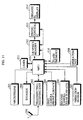
- Fig. 9 illustrates the schematic configuration of a portable telephone set.
- An MPU (Microprocessor Unit) 209 carries out the overall control of the portable telephone set.
- An antenna 201 transmits and receives electric waves.
- a transmitting/receiving unit 202 receives the electric waves, and transmits the contents of the receiving to the MPU 209. Further, the transmitting/receiving unit 202 transmits a transmission signal outputted from the MPU 209 with the transmission signal on the electric waves.
- a microphone 203 feeds an audio signal to the MPU 209.
- a speaker 204 outputs as an audio the audio signal outputted from the MPU 209.
- a first camera 205 is a camera mounted on a front surface of the main body of the portable telephone set provided with an organic EL display 214, and sends to the MPU 209 a video which it has picked up.
- a second camera 206 is a camera mounted on a rear surface of the main body of the portable telephone set, and sends to the MPU 209 a video which it has picked up.
- the video picked up by the camera 205 or 206 is displayed on the organic EL display 214 in place of the content of the display at the time of a normal mode.
- An operation unit 208 is provided in the main body of the portable telephone set, and comprises various buttons 221 and various switches 222, as shown in Fig. 10.
- a timer 211 is used for luminance control, described later.
- a flash memory 210 stores data to be stored even when the power is turned off.
- a graphics memory 212 stores image data to be displayed on the display. Image data is written into a predetermined address in the graphics memory 212 on the basis of image data outputted from the MPU 209 and a writing control signal. Pixel data representing a corresponding pixel is outputted at the timing of scanning in conformity with a display period of the organic EL display 214 from the graphics memory 212.
- a timing control IC 213 feeds image data and a driving signal to the organic EL display 214, and displays a video on the organic EL display 214.
- the timing control IC 213 comprises a luminance control circuit.
- Fig. 10 illustrates the configuration of the luminance control circuit provided in the timing control IC 213, and the MPU 209 for controlling a luminance for the whole screen and its peripheral device.
- the luminance control circuit shown in Fig. 10 is approximately the same as the luminance control circuit shown in Fig. 3 except that a multiplier 41 for controlling a luminance for the whole screen (a display luminance) is provided in a reference voltage control circuit 1.
- An whole luminance control signal W _ Gain given to the multiplier 41 is generated by the MPU 209.
- the various buttons 208 and the various switches 222 which are provided in the operation unit 208 are connected to the MPU 209.
- the MPU 209 comprises the timer 211.
- the cameras 205 and 206 are connected to the MPU 209. Each of the cameras 205 and 206 has an automatic exposure control function. In this example, exposure time information is sent to the MPU 209 from the first camera 205 mounted on the front surface of the main body of the portable telephone set.
- the MPU 209 estimates peripheral brightness under current environments in which the portable telephone set is used on the basis of the exposure time information from the first camera 205, to generate the whole luminance control signal W _Gain.
- the whole luminance control signal W _Gain takes a value between 2.0 and 0.5, for example.
- the whole luminance control signal W _Gain is reduced.
- a gain outputted from the multiplier 41 becomes smaller than a gain calculated by the gain calculation circuit 14, and a white-side reference voltage R _Refw' after control becomes high, so that the display luminance becomes low.
- the whole luminance control signal W _Gain is increased.
- the gain outputted from the multiplier 41 becomes larger than the gain calculated by the gain calculation circuit 14, and the white-side reference voltage R _Refw' after control becomes low, so that the display luminance becomes high.
- the above-mentioned control may be carried out using AGC gain information relating to the first camera 205 in place of the exposure time information relating to the first camera 205.
- AGC gain information relating to the first camera 205 in place of the exposure time information relating to the first camera 205.
- the AGC gain is large, it is judged that the peripheral brightness is low, to reduce the whole luminance control signal W _Gain.
- the AGC gain is small, it is judged that the peripheral brightness is high, to increase the whole luminance control signal W _Gain.
- the MPU 209 reduces, when the various buttons 221 or the various switches 222 which are provided in the operation unit 208 are operated, the whole luminance control signal W _Gain is reduced, to increase the display luminance.
- the whole luminance control signal W _Gain is increased, to reduce the display luminance.
- the timer 211 It is judged using the timer 211 whether or not a predetermined time period has elapsed. Specifically, the timer 211 is reset when the buttons 221 or the switches 222 are operated, to automatically start measurement of time. The luminance for the screen is controlled depending on the time measured by the timer 211. When not less than the predetermined time period has elapsed, the display luminance is reduced by half.
- Fig. 11 illustrates the schematic configuration of a portable telephone set.
- the same components as those shown in Fig. 9 are assigned the same reference numerals and hence, the description thereof is not repeated.
- the portable telephone set differs from the portable telephone set shown in Fig. 9 in that a direction sensor 207 for sensing the direction (upward, downward, sideward, etc.) of a display surface of an organic EL display 214 is provided.
- a direction sensor 207 for sensing the direction (upward, downward, sideward, etc.) of a display surface of an organic EL display 214 is provided.
- display luminance control based on exposure time information from a first camera 205 is not carried out.
- Fig. 12 illustrates the configuration of a luminance control circuit provided in a timing control IC 213, and an MPU 209 for controlling a luminance for the whole screen and its peripheral device.
- Fig. 12 the same components as those shown in Fig. 3 are assigned the same reference numerals and hence, the description thereof is not repeated.
- the luminance control circuit shown in Fig. 12 is approximately the same as the luminance control circuit shown in Fig. 3, it differs from the luminance control circuit shown in Fig. 3 in that a multiplier 41 for controlling a luminance for the whole screen (a display luminance) is provided in a reference voltage control circuit 1.
- a whole luminance control signal W _Gain given to the multiplier 41 is generated by the MPU 209.
- buttons 221 and various switches 222 which are provided in an operation unit 208 are connected to the MPU 209.
- the MPU 209 comprises a timer 211.
- the direction sensor 207 is connected to the MPU 209.
- the MPU 209 estimates the direction (upward, downward, sideward, etc.) of the display surface of the organic EL display 214 on the basis of a detection signal of the direction sensor 207, to generate a whole luminance control signal W _-Gain.
- the whole luminance control signal W _Gain takes a value between 2.0 and 0.5, for example.
- the whole luminance control signal W _Gain is reduced, thereby making the display luminance higher.
- the whole luminance control signal W _Gain is controlled to a small value when the display surface of the organic EL display is directed upward, is controlled to a large value when the display surface of the organic EL display 214 is directed downward, and is controlled to an intermediate value when the display surface of the organic EL display 214 is directed sideward.
- the MPU 209 reduces the whole luminance control signal W _Gain when the various buttons 221 or the various switches 222 which are provided in the operation unit 208 are operated, as in the above-mentioned third embodiment, thereby making the display luminance higher.
- the whole luminance control signal W _Gain is increased, thereby reducing the display luminance.
- the direction (upward, downward, sideward, etc.) of the display surface of the. organic EL display 214 may be detected from the exposure times and the AGC gains of two cameras 205 and 206.
- the exposure time of the first camera 205 attached to the front surface of the main body of the portable telephone set is shorter than the exposure time of the second camera 206 attached to the rear surface of the main body of the portable telephone set (the AGC gain thereof is reduced when the exposure times are the same).
- the exposure time of the second camera 206 attached to the rear surface of the main body of the portable telephone set is shorter than the exposure time of the first camera 205 attached to the front surface of the main body of the portable telephone set (the AGC gain thereof is reduced when the exposure times are the same).
- the direction of the display surface of the organic EL display 214 can be judged by the exposure times and the AGC gains of the two cameras 205 and 206.
Applications Claiming Priority (5)
| Application Number | Priority Date | Filing Date | Title |
|---|---|---|---|
| JP2001400238 | 2001-12-28 | ||
| JP2001400238 | 2001-12-28 | ||
| JP2002091796A JP2003255901A (ja) | 2001-12-28 | 2002-03-28 | 有機elディスプレイの輝度制御方法および輝度制御回路 |
| JP2002091796 | 2002-03-28 | ||
| PCT/JP2002/013728 WO2003058593A1 (fr) | 2001-12-28 | 2002-12-26 | Procede de commande de la luminance d'un ecran electroluminescent organique et circuit de commande de luminance |
Publications (3)
| Publication Number | Publication Date |
|---|---|
| EP1469448A1 true EP1469448A1 (fr) | 2004-10-20 |
| EP1469448A4 EP1469448A4 (fr) | 2009-04-15 |
| EP1469448B1 EP1469448B1 (fr) | 2015-10-21 |
Family
ID=26625384
Family Applications (1)
| Application Number | Title | Priority Date | Filing Date |
|---|---|---|---|
| EP02792039.6A Expired - Fee Related EP1469448B1 (fr) | 2001-12-28 | 2002-12-26 | Procédé de commande de la luminance d'un ecran electroluminescent organique et circuit de commande de luminance |
Country Status (4)
| Country | Link |
|---|---|
| US (2) | US7304654B2 (fr) |
| EP (1) | EP1469448B1 (fr) |
| JP (1) | JP2003255901A (fr) |
| WO (1) | WO2003058593A1 (fr) |
Cited By (54)
| Publication number | Priority date | Publication date | Assignee | Title |
|---|---|---|---|---|
| WO2005022899A2 (fr) | 2003-08-29 | 2005-03-10 | Casio Computer Co., Ltd. | Dispositif d'imagerie et procede d'imagerie |
| WO2006108277A1 (fr) | 2005-04-12 | 2006-10-19 | Ignis Innovation Inc. | Procédé et système permettant de compenser des non-uniformités dans des écrans à dispositifs électroluminescents |
| EP1662467A4 (fr) * | 2003-08-05 | 2008-01-23 | Toshiba Matsushita Display Tec | Circuit et procede de commande d'un dispositif d'affichage auto-lumineux |
| EP1942485A2 (fr) * | 2007-01-05 | 2008-07-09 | Samsung Electronics Co., Ltd. | Dispositif d'affichage électroluminescent organique et son procédé de commande |
| US8816946B2 (en) | 2004-12-15 | 2014-08-26 | Ignis Innovation Inc. | Method and system for programming, calibrating and driving a light emitting device display |
| US8907991B2 (en) | 2010-12-02 | 2014-12-09 | Ignis Innovation Inc. | System and methods for thermal compensation in AMOLED displays |
| US8914246B2 (en) | 2009-11-30 | 2014-12-16 | Ignis Innovation Inc. | System and methods for aging compensation in AMOLED displays |
| US8922544B2 (en) | 2012-05-23 | 2014-12-30 | Ignis Innovation Inc. | Display systems with compensation for line propagation delay |
| US8941697B2 (en) | 2003-09-23 | 2015-01-27 | Ignis Innovation Inc. | Circuit and method for driving an array of light emitting pixels |
| US9059117B2 (en) | 2009-12-01 | 2015-06-16 | Ignis Innovation Inc. | High resolution pixel architecture |
| US9093029B2 (en) | 2011-05-20 | 2015-07-28 | Ignis Innovation Inc. | System and methods for extraction of threshold and mobility parameters in AMOLED displays |
| US9093028B2 (en) | 2009-12-06 | 2015-07-28 | Ignis Innovation Inc. | System and methods for power conservation for AMOLED pixel drivers |
| US9111485B2 (en) | 2009-06-16 | 2015-08-18 | Ignis Innovation Inc. | Compensation technique for color shift in displays |
| US9125278B2 (en) | 2006-08-15 | 2015-09-01 | Ignis Innovation Inc. | OLED luminance degradation compensation |
| US9633597B2 (en) | 2006-04-19 | 2017-04-25 | Ignis Innovation Inc. | Stable driving scheme for active matrix displays |
| US9640112B2 (en) | 2011-05-26 | 2017-05-02 | Ignis Innovation Inc. | Adaptive feedback system for compensating for aging pixel areas with enhanced estimation speed |
| US9685114B2 (en) | 2012-12-11 | 2017-06-20 | Ignis Innovation Inc. | Pixel circuits for AMOLED displays |
| US9721512B2 (en) | 2013-03-15 | 2017-08-01 | Ignis Innovation Inc. | AMOLED displays with multiple readout circuits |
| US9741282B2 (en) | 2013-12-06 | 2017-08-22 | Ignis Innovation Inc. | OLED display system and method |
| US9747834B2 (en) | 2012-05-11 | 2017-08-29 | Ignis Innovation Inc. | Pixel circuits including feedback capacitors and reset capacitors, and display systems therefore |
| US9761170B2 (en) | 2013-12-06 | 2017-09-12 | Ignis Innovation Inc. | Correction for localized phenomena in an image array |
| US9773441B2 (en) | 2010-02-04 | 2017-09-26 | Ignis Innovation Inc. | System and methods for extracting correlation curves for an organic light emitting device |
| US9773439B2 (en) | 2011-05-27 | 2017-09-26 | Ignis Innovation Inc. | Systems and methods for aging compensation in AMOLED displays |
| US9786223B2 (en) | 2012-12-11 | 2017-10-10 | Ignis Innovation Inc. | Pixel circuits for AMOLED displays |
| US9792857B2 (en) | 2012-02-03 | 2017-10-17 | Ignis Innovation Inc. | Driving system for active-matrix displays |
| US9799246B2 (en) | 2011-05-20 | 2017-10-24 | Ignis Innovation Inc. | System and methods for extraction of threshold and mobility parameters in AMOLED displays |
| US9818323B2 (en) | 2013-03-14 | 2017-11-14 | Ignis Innovation Inc. | Re-interpolation with edge detection for extracting an aging pattern for AMOLED displays |
| US9830857B2 (en) | 2013-01-14 | 2017-11-28 | Ignis Innovation Inc. | Cleaning common unwanted signals from pixel measurements in emissive displays |
| US9881532B2 (en) | 2010-02-04 | 2018-01-30 | Ignis Innovation Inc. | System and method for extracting correlation curves for an organic light emitting device |
| US9947293B2 (en) | 2015-05-27 | 2018-04-17 | Ignis Innovation Inc. | Systems and methods of reduced memory bandwidth compensation |
| US9990882B2 (en) | 2013-08-12 | 2018-06-05 | Ignis Innovation Inc. | Compensation accuracy |
| US10012678B2 (en) | 2004-12-15 | 2018-07-03 | Ignis Innovation Inc. | Method and system for programming, calibrating and/or compensating, and driving an LED display |
| US10013907B2 (en) | 2004-12-15 | 2018-07-03 | Ignis Innovation Inc. | Method and system for programming, calibrating and/or compensating, and driving an LED display |
| US10019941B2 (en) | 2005-09-13 | 2018-07-10 | Ignis Innovation Inc. | Compensation technique for luminance degradation in electro-luminance devices |
| US10074304B2 (en) | 2015-08-07 | 2018-09-11 | Ignis Innovation Inc. | Systems and methods of pixel calibration based on improved reference values |
| US10078984B2 (en) | 2005-02-10 | 2018-09-18 | Ignis Innovation Inc. | Driving circuit for current programmed organic light-emitting diode displays |
| US10089924B2 (en) | 2011-11-29 | 2018-10-02 | Ignis Innovation Inc. | Structural and low-frequency non-uniformity compensation |
| US10089921B2 (en) | 2010-02-04 | 2018-10-02 | Ignis Innovation Inc. | System and methods for extracting correlation curves for an organic light emitting device |
| US10163401B2 (en) | 2010-02-04 | 2018-12-25 | Ignis Innovation Inc. | System and methods for extracting correlation curves for an organic light emitting device |
| US10176736B2 (en) | 2010-02-04 | 2019-01-08 | Ignis Innovation Inc. | System and methods for extracting correlation curves for an organic light emitting device |
| US10181282B2 (en) | 2015-01-23 | 2019-01-15 | Ignis Innovation Inc. | Compensation for color variations in emissive devices |
| US10192479B2 (en) | 2014-04-08 | 2019-01-29 | Ignis Innovation Inc. | Display system using system level resources to calculate compensation parameters for a display module in a portable device |
| USRE47257E1 (en) | 2004-06-29 | 2019-02-26 | Ignis Innovation Inc. | Voltage-programming scheme for current-driven AMOLED displays |
| US10235933B2 (en) | 2005-04-12 | 2019-03-19 | Ignis Innovation Inc. | System and method for compensation of non-uniformities in light emitting device displays |
| US10304390B2 (en) | 2009-11-30 | 2019-05-28 | Ignis Innovation Inc. | System and methods for aging compensation in AMOLED displays |
| US10311780B2 (en) | 2015-05-04 | 2019-06-04 | Ignis Innovation Inc. | Systems and methods of optical feedback |
| US10319307B2 (en) | 2009-06-16 | 2019-06-11 | Ignis Innovation Inc. | Display system with compensation techniques and/or shared level resources |
| US10388221B2 (en) | 2005-06-08 | 2019-08-20 | Ignis Innovation Inc. | Method and system for driving a light emitting device display |
| US10439159B2 (en) | 2013-12-25 | 2019-10-08 | Ignis Innovation Inc. | Electrode contacts |
| US10475379B2 (en) | 2011-05-20 | 2019-11-12 | Ignis Innovation Inc. | Charged-based compensation and parameter extraction in AMOLED displays |
| US10573231B2 (en) | 2010-02-04 | 2020-02-25 | Ignis Innovation Inc. | System and methods for extracting correlation curves for an organic light emitting device |
| US10699613B2 (en) | 2009-11-30 | 2020-06-30 | Ignis Innovation Inc. | Resetting cycle for aging compensation in AMOLED displays |
| US10867536B2 (en) | 2013-04-22 | 2020-12-15 | Ignis Innovation Inc. | Inspection system for OLED display panels |
| US10996258B2 (en) | 2009-11-30 | 2021-05-04 | Ignis Innovation Inc. | Defect detection and correction of pixel circuits for AMOLED displays |
Families Citing this family (28)
| Publication number | Priority date | Publication date | Assignee | Title |
|---|---|---|---|---|
| JP4534031B2 (ja) * | 2003-03-06 | 2010-09-01 | グローバル・オーエルイーディー・テクノロジー・リミテッド・ライアビリティ・カンパニー | 有機el表示装置 |
| KR100611882B1 (ko) * | 2004-06-25 | 2006-08-11 | 삼성에스디아이 주식회사 | 영상 표시장치 및 방법 |
| CN100423063C (zh) * | 2004-06-25 | 2008-10-01 | 三洋电机株式会社 | 自发光型显示器的信号处理电路和信号处理方法 |
| JP4530742B2 (ja) * | 2004-07-01 | 2010-08-25 | Hoya株式会社 | モニタ制御装置 |
| JP4457791B2 (ja) * | 2004-07-20 | 2010-04-28 | パナソニック株式会社 | 表示装置 |
| JP4274070B2 (ja) * | 2004-07-23 | 2009-06-03 | ソニー株式会社 | 表示装置及びその駆動方法 |
| EP1622119A1 (fr) * | 2004-07-29 | 2006-02-01 | Deutsche Thomson-Brandt Gmbh | Procédé et appareil pour contrôle du niveau de puissance et/ou du contraste d'un dispositif d'affichage |
| KR100846954B1 (ko) * | 2004-08-30 | 2008-07-17 | 삼성에스디아이 주식회사 | 발광 표시장치와 그의 구동방법 |
| KR100670137B1 (ko) * | 2004-10-08 | 2007-01-16 | 삼성에스디아이 주식회사 | 디지털/아날로그 컨버터와 이를 이용한 표시 장치 및 그표시 패널과 구동 방법 |
| KR100658619B1 (ko) | 2004-10-08 | 2006-12-15 | 삼성에스디아이 주식회사 | 디지털/아날로그 컨버터와 이를 이용한 표시 장치 및 그표시 패널과 구동 방법 |
| US9275579B2 (en) | 2004-12-15 | 2016-03-01 | Ignis Innovation Inc. | System and methods for extraction of threshold and mobility parameters in AMOLED displays |
| US9280933B2 (en) | 2004-12-15 | 2016-03-08 | Ignis Innovation Inc. | System and methods for extraction of threshold and mobility parameters in AMOLED displays |
| US9171500B2 (en) | 2011-05-20 | 2015-10-27 | Ignis Innovation Inc. | System and methods for extraction of parasitic parameters in AMOLED displays |
| JP2006259573A (ja) * | 2005-03-18 | 2006-09-28 | Seiko Epson Corp | 有機el装置及びその駆動方法並びに電子機器 |
| JP2006267149A (ja) * | 2005-03-22 | 2006-10-05 | Sanyo Electric Co Ltd | 表示装置 |
| US8659511B2 (en) | 2005-08-10 | 2014-02-25 | Samsung Display Co., Ltd. | Data driver, organic light emitting display device using the same, and method of driving the organic light emitting display device |
| KR100658265B1 (ko) * | 2005-08-10 | 2006-12-14 | 삼성에스디아이 주식회사 | 데이터 구동회로와 이를 이용한 발광 표시장치 및 그의구동방법 |
| JP5248750B2 (ja) * | 2006-03-14 | 2013-07-31 | グローバル・オーエルイーディー・テクノロジー・リミテッド・ライアビリティ・カンパニー | 表示装置の駆動装置及び駆動方法 |
| KR101279117B1 (ko) * | 2006-06-30 | 2013-06-26 | 엘지디스플레이 주식회사 | 유기발광다이오드 표시소자 및 그의 구동 방법 |
| KR100857672B1 (ko) * | 2007-02-02 | 2008-09-08 | 삼성에스디아이 주식회사 | 유기전계발광표시장치 및 그의 구동방법 |
| KR100844775B1 (ko) * | 2007-02-23 | 2008-07-07 | 삼성에스디아이 주식회사 | 유기 전계발광 표시장치 |
| KR100902219B1 (ko) | 2007-12-05 | 2009-06-11 | 삼성모바일디스플레이주식회사 | 유기전계발광 표시장치 |
| CA2696778A1 (fr) | 2010-03-17 | 2011-09-17 | Ignis Innovation Inc. | Procedes d'extraction des parametres d'uniformite de duree de vie |
| JP2013003238A (ja) | 2011-06-14 | 2013-01-07 | Sony Corp | 映像信号処理回路、映像信号処理方法、表示装置、及び、電子機器 |
| JP6167324B2 (ja) * | 2012-07-25 | 2017-07-26 | 株式会社Joled | 表示装置、画像処理装置、および画像処理方法 |
| WO2014108879A1 (fr) | 2013-01-14 | 2014-07-17 | Ignis Innovation Inc. | Schéma d'entraînement pour afficheurs émissifs comprenant une compensation de variations de transistor d'entraînement |
| KR102105631B1 (ko) * | 2013-12-19 | 2020-04-28 | 엘지디스플레이 주식회사 | 표시장치 |
| JP7386035B2 (ja) | 2019-10-09 | 2023-11-24 | JDI Design and Development 合同会社 | 電流制限回路、表示装置、及び電流制限方法 |
Citations (3)
| Publication number | Priority date | Publication date | Assignee | Title |
|---|---|---|---|---|
| JPH10108021A (ja) * | 1996-09-30 | 1998-04-24 | Sony Corp | プリンタ装置 |
| WO1998039914A1 (fr) * | 1997-03-06 | 1998-09-11 | Matsushita Electric Industrial Co., Ltd. | Circuit de correction de la qualite d'image pour signaux video |
| US20010036312A1 (en) * | 2000-03-16 | 2001-11-01 | Tetsuya Shigeta | Luminance gradation correcting apparatus for a video signal |
Family Cites Families (29)
| Publication number | Priority date | Publication date | Assignee | Title |
|---|---|---|---|---|
| JPS5478124A (en) * | 1977-12-03 | 1979-06-22 | Nippon Chemical Ind | Automatic exposure control camera display unit |
| JPH06350943A (ja) * | 1993-06-10 | 1994-12-22 | Fujitsu General Ltd | 画像処理回路 |
| JP3606920B2 (ja) * | 1994-10-26 | 2005-01-05 | 株式会社リコー | 表示制御装置 |
| JPH08186761A (ja) * | 1994-12-30 | 1996-07-16 | Sony Corp | ビデオカメラ装置及びビデオカメラ露出制御方法 |
| JP3791029B2 (ja) * | 1995-11-22 | 2006-06-28 | ソニー株式会社 | 画像信号処理装置および方法 |
| US5668569A (en) * | 1996-04-05 | 1997-09-16 | Rainbow Displays Inc. | Tiled, flat-panel displays with luminance-correcting capability |
| US6271825B1 (en) * | 1996-04-23 | 2001-08-07 | Rainbow Displays, Inc. | Correction methods for brightness in electronic display |
| CN1197427A (zh) * | 1996-07-09 | 1998-10-28 | 塞科拉系统株式会社 | 曝光装置,曝光方法以及印刷装置 |
| JPH10268832A (ja) * | 1997-03-26 | 1998-10-09 | Matsushita Electric Ind Co Ltd | 映像表示装置 |
| KR20010033768A (ko) * | 1997-12-31 | 2001-04-25 | 프레데릭 티. 바우어 | 자동차 영상장치 |
| JPH11275386A (ja) * | 1998-03-20 | 1999-10-08 | Matsushita Electric Ind Co Ltd | 自動輝度調整装置 |
| AU753051B2 (en) | 1998-03-06 | 2002-10-03 | Matsushita Electric Industrial Co., Ltd. | Automatic luminance adjustment device and method |
| JP2000056730A (ja) * | 1998-06-05 | 2000-02-25 | Canon Inc | 画像形成装置及び画像形成方法 |
| JP2000322022A (ja) | 1998-06-05 | 2000-11-24 | Canon Inc | 画像形成装置及び画像形成方法 |
| JP2000089712A (ja) * | 1998-09-16 | 2000-03-31 | Canon Inc | 表示装置及びその表示制御方法 |
| JP2000221945A (ja) | 1999-02-04 | 2000-08-11 | Victor Co Of Japan Ltd | マトリクス型表示装置 |
| JP4073107B2 (ja) | 1999-03-18 | 2008-04-09 | 三洋電機株式会社 | アクティブ型el表示装置 |
| US6404145B1 (en) * | 1999-04-06 | 2002-06-11 | Fuji Photo Film Co., Ltd. | Apparatus for and method of controlling backlight for liquid crystal display |
| JP2001022319A (ja) * | 1999-07-09 | 2001-01-26 | Matsushita Electric Ind Co Ltd | 携帯端末における表示範囲の調整装置及び調整方法 |
| JP2001086393A (ja) | 1999-09-10 | 2001-03-30 | Canon Inc | 移動体通信装置 |
| JP2001092412A (ja) * | 1999-09-17 | 2001-04-06 | Pioneer Electronic Corp | アクティブマトリクス型表示装置 |
| JP4202555B2 (ja) | 1999-10-04 | 2008-12-24 | 富士フイルム株式会社 | 光量評価機能付き表示装置および光供給制御方法 |
| JP3767292B2 (ja) * | 1999-12-22 | 2006-04-19 | セイコーエプソン株式会社 | 表示装置の駆動方法 |
| JP4801260B2 (ja) | 2000-01-17 | 2011-10-26 | 株式会社半導体エネルギー研究所 | 電気器具 |
| JP2001320454A (ja) | 2000-05-11 | 2001-11-16 | Fuji Photo Film Co Ltd | カメラ付き携帯電話機 |
| JP2001350450A (ja) * | 2000-06-05 | 2001-12-21 | Matsushita Electric Ind Co Ltd | 液晶表示装置 |
| US6809838B1 (en) * | 2000-10-19 | 2004-10-26 | Eastman Kodak Company | Transforms for display or printing digital images |
| US7102632B2 (en) * | 2001-06-05 | 2006-09-05 | Eastman Kodak Company | Method for saving power in an organic electroluminescent display |
| JP3726733B2 (ja) * | 2001-10-16 | 2005-12-14 | コニカミノルタフォトイメージング株式会社 | 撮影システム |
-
2002
- 2002-03-28 JP JP2002091796A patent/JP2003255901A/ja active Pending
- 2002-12-26 EP EP02792039.6A patent/EP1469448B1/fr not_active Expired - Fee Related
- 2002-12-26 WO PCT/JP2002/013728 patent/WO2003058593A1/fr active Application Filing
- 2002-12-26 US US10/500,374 patent/US7304654B2/en not_active Expired - Fee Related
-
2007
- 2007-11-07 US US11/979,668 patent/US20080084433A1/en not_active Abandoned
Patent Citations (3)
| Publication number | Priority date | Publication date | Assignee | Title |
|---|---|---|---|---|
| JPH10108021A (ja) * | 1996-09-30 | 1998-04-24 | Sony Corp | プリンタ装置 |
| WO1998039914A1 (fr) * | 1997-03-06 | 1998-09-11 | Matsushita Electric Industrial Co., Ltd. | Circuit de correction de la qualite d'image pour signaux video |
| US20010036312A1 (en) * | 2000-03-16 | 2001-11-01 | Tetsuya Shigeta | Luminance gradation correcting apparatus for a video signal |
Non-Patent Citations (1)
| Title |
|---|
| See also references of WO03058593A1 * |
Cited By (108)
| Publication number | Priority date | Publication date | Assignee | Title |
|---|---|---|---|---|
| US7592981B2 (en) | 2003-08-05 | 2009-09-22 | Toshiba Matsushita Display Technology Co., Ltd. | Circuit for driving self-luminous display device and method for driving the same |
| EP1662467A4 (fr) * | 2003-08-05 | 2008-01-23 | Toshiba Matsushita Display Tec | Circuit et procede de commande d'un dispositif d'affichage auto-lumineux |
| US7436446B2 (en) | 2003-08-29 | 2008-10-14 | Casio Computer Co., Ltd. | Imaging device equipped with automatic exposure control function |
| WO2005022899A3 (fr) * | 2003-08-29 | 2005-06-02 | Casio Computer Co Ltd | Dispositif d'imagerie et procede d'imagerie |
| WO2005022899A2 (fr) | 2003-08-29 | 2005-03-10 | Casio Computer Co., Ltd. | Dispositif d'imagerie et procede d'imagerie |
| US9852689B2 (en) | 2003-09-23 | 2017-12-26 | Ignis Innovation Inc. | Circuit and method for driving an array of light emitting pixels |
| US10089929B2 (en) | 2003-09-23 | 2018-10-02 | Ignis Innovation Inc. | Pixel driver circuit with load-balance in current mirror circuit |
| US8941697B2 (en) | 2003-09-23 | 2015-01-27 | Ignis Innovation Inc. | Circuit and method for driving an array of light emitting pixels |
| USRE47257E1 (en) | 2004-06-29 | 2019-02-26 | Ignis Innovation Inc. | Voltage-programming scheme for current-driven AMOLED displays |
| US10013907B2 (en) | 2004-12-15 | 2018-07-03 | Ignis Innovation Inc. | Method and system for programming, calibrating and/or compensating, and driving an LED display |
| US10699624B2 (en) | 2004-12-15 | 2020-06-30 | Ignis Innovation Inc. | Method and system for programming, calibrating and/or compensating, and driving an LED display |
| US9970964B2 (en) | 2004-12-15 | 2018-05-15 | Ignis Innovation Inc. | Method and system for programming, calibrating and driving a light emitting device display |
| US8994625B2 (en) | 2004-12-15 | 2015-03-31 | Ignis Innovation Inc. | Method and system for programming, calibrating and driving a light emitting device display |
| US8816946B2 (en) | 2004-12-15 | 2014-08-26 | Ignis Innovation Inc. | Method and system for programming, calibrating and driving a light emitting device display |
| US10012678B2 (en) | 2004-12-15 | 2018-07-03 | Ignis Innovation Inc. | Method and system for programming, calibrating and/or compensating, and driving an LED display |
| US10078984B2 (en) | 2005-02-10 | 2018-09-18 | Ignis Innovation Inc. | Driving circuit for current programmed organic light-emitting diode displays |
| WO2006108277A1 (fr) | 2005-04-12 | 2006-10-19 | Ignis Innovation Inc. | Procédé et système permettant de compenser des non-uniformités dans des écrans à dispositifs électroluminescents |
| US10235933B2 (en) | 2005-04-12 | 2019-03-19 | Ignis Innovation Inc. | System and method for compensation of non-uniformities in light emitting device displays |
| US7868857B2 (en) | 2005-04-12 | 2011-01-11 | Ignis Innovation Inc. | Method and system for compensation of non-uniformities in light emitting device displays |
| EP1869657A4 (fr) * | 2005-04-12 | 2009-12-23 | Ignis Innovation Inc | Procédé et système permettant de compenser des non-uniformités dans des écrans à dispositifs électroluminescents |
| EP1869657A1 (fr) * | 2005-04-12 | 2007-12-26 | Ignis Innovation Inc. | Procédé et système permettant de compenser des non-uniformités dans des écrans à dispositifs électroluminescents |
| US10388221B2 (en) | 2005-06-08 | 2019-08-20 | Ignis Innovation Inc. | Method and system for driving a light emitting device display |
| US10019941B2 (en) | 2005-09-13 | 2018-07-10 | Ignis Innovation Inc. | Compensation technique for luminance degradation in electro-luminance devices |
| US9842544B2 (en) | 2006-04-19 | 2017-12-12 | Ignis Innovation Inc. | Stable driving scheme for active matrix displays |
| US10453397B2 (en) | 2006-04-19 | 2019-10-22 | Ignis Innovation Inc. | Stable driving scheme for active matrix displays |
| US9633597B2 (en) | 2006-04-19 | 2017-04-25 | Ignis Innovation Inc. | Stable driving scheme for active matrix displays |
| US10127860B2 (en) | 2006-04-19 | 2018-11-13 | Ignis Innovation Inc. | Stable driving scheme for active matrix displays |
| US9125278B2 (en) | 2006-08-15 | 2015-09-01 | Ignis Innovation Inc. | OLED luminance degradation compensation |
| US10325554B2 (en) | 2006-08-15 | 2019-06-18 | Ignis Innovation Inc. | OLED luminance degradation compensation |
| US8194010B2 (en) | 2007-01-05 | 2012-06-05 | Samsung Electronics Co., Ltd. | Organic light emitting display device and method of driving the same |
| EP1942485A2 (fr) * | 2007-01-05 | 2008-07-09 | Samsung Electronics Co., Ltd. | Dispositif d'affichage électroluminescent organique et son procédé de commande |
| EP1942485A3 (fr) * | 2007-01-05 | 2009-03-18 | Samsung Electronics Co., Ltd. | Dispositif d'affichage électroluminescent organique et son procédé de commande |
| CN101217021B (zh) * | 2007-01-05 | 2013-03-06 | 三星显示有限公司 | 有机发光显示装置及其驱动方法 |
| US10319307B2 (en) | 2009-06-16 | 2019-06-11 | Ignis Innovation Inc. | Display system with compensation techniques and/or shared level resources |
| US9117400B2 (en) | 2009-06-16 | 2015-08-25 | Ignis Innovation Inc. | Compensation technique for color shift in displays |
| US9111485B2 (en) | 2009-06-16 | 2015-08-18 | Ignis Innovation Inc. | Compensation technique for color shift in displays |
| US10553141B2 (en) | 2009-06-16 | 2020-02-04 | Ignis Innovation Inc. | Compensation technique for color shift in displays |
| US10304390B2 (en) | 2009-11-30 | 2019-05-28 | Ignis Innovation Inc. | System and methods for aging compensation in AMOLED displays |
| US10699613B2 (en) | 2009-11-30 | 2020-06-30 | Ignis Innovation Inc. | Resetting cycle for aging compensation in AMOLED displays |
| US8914246B2 (en) | 2009-11-30 | 2014-12-16 | Ignis Innovation Inc. | System and methods for aging compensation in AMOLED displays |
| US9786209B2 (en) | 2009-11-30 | 2017-10-10 | Ignis Innovation Inc. | System and methods for aging compensation in AMOLED displays |
| US10679533B2 (en) | 2009-11-30 | 2020-06-09 | Ignis Innovation Inc. | System and methods for aging compensation in AMOLED displays |
| US10996258B2 (en) | 2009-11-30 | 2021-05-04 | Ignis Innovation Inc. | Defect detection and correction of pixel circuits for AMOLED displays |
| US9059117B2 (en) | 2009-12-01 | 2015-06-16 | Ignis Innovation Inc. | High resolution pixel architecture |
| US9093028B2 (en) | 2009-12-06 | 2015-07-28 | Ignis Innovation Inc. | System and methods for power conservation for AMOLED pixel drivers |
| US9773441B2 (en) | 2010-02-04 | 2017-09-26 | Ignis Innovation Inc. | System and methods for extracting correlation curves for an organic light emitting device |
| US9881532B2 (en) | 2010-02-04 | 2018-01-30 | Ignis Innovation Inc. | System and method for extracting correlation curves for an organic light emitting device |
| US11200839B2 (en) | 2010-02-04 | 2021-12-14 | Ignis Innovation Inc. | System and methods for extracting correlation curves for an organic light emitting device |
| US10395574B2 (en) | 2010-02-04 | 2019-08-27 | Ignis Innovation Inc. | System and methods for extracting correlation curves for an organic light emitting device |
| US10176736B2 (en) | 2010-02-04 | 2019-01-08 | Ignis Innovation Inc. | System and methods for extracting correlation curves for an organic light emitting device |
| US10163401B2 (en) | 2010-02-04 | 2018-12-25 | Ignis Innovation Inc. | System and methods for extracting correlation curves for an organic light emitting device |
| US10971043B2 (en) | 2010-02-04 | 2021-04-06 | Ignis Innovation Inc. | System and method for extracting correlation curves for an organic light emitting device |
| US10089921B2 (en) | 2010-02-04 | 2018-10-02 | Ignis Innovation Inc. | System and methods for extracting correlation curves for an organic light emitting device |
| US10032399B2 (en) | 2010-02-04 | 2018-07-24 | Ignis Innovation Inc. | System and methods for extracting correlation curves for an organic light emitting device |
| US10573231B2 (en) | 2010-02-04 | 2020-02-25 | Ignis Innovation Inc. | System and methods for extracting correlation curves for an organic light emitting device |
| US10460669B2 (en) | 2010-12-02 | 2019-10-29 | Ignis Innovation Inc. | System and methods for thermal compensation in AMOLED displays |
| US8907991B2 (en) | 2010-12-02 | 2014-12-09 | Ignis Innovation Inc. | System and methods for thermal compensation in AMOLED displays |
| US9997110B2 (en) | 2010-12-02 | 2018-06-12 | Ignis Innovation Inc. | System and methods for thermal compensation in AMOLED displays |
| US10580337B2 (en) | 2011-05-20 | 2020-03-03 | Ignis Innovation Inc. | System and methods for extraction of threshold and mobility parameters in AMOLED displays |
| US10032400B2 (en) | 2011-05-20 | 2018-07-24 | Ignis Innovation Inc. | System and methods for extraction of threshold and mobility parameters in AMOLED displays |
| US9799248B2 (en) | 2011-05-20 | 2017-10-24 | Ignis Innovation Inc. | System and methods for extraction of threshold and mobility parameters in AMOLED displays |
| US10127846B2 (en) | 2011-05-20 | 2018-11-13 | Ignis Innovation Inc. | System and methods for extraction of threshold and mobility parameters in AMOLED displays |
| US10325537B2 (en) | 2011-05-20 | 2019-06-18 | Ignis Innovation Inc. | System and methods for extraction of threshold and mobility parameters in AMOLED displays |
| US9799246B2 (en) | 2011-05-20 | 2017-10-24 | Ignis Innovation Inc. | System and methods for extraction of threshold and mobility parameters in AMOLED displays |
| US9093029B2 (en) | 2011-05-20 | 2015-07-28 | Ignis Innovation Inc. | System and methods for extraction of threshold and mobility parameters in AMOLED displays |
| US10475379B2 (en) | 2011-05-20 | 2019-11-12 | Ignis Innovation Inc. | Charged-based compensation and parameter extraction in AMOLED displays |
| US10706754B2 (en) | 2011-05-26 | 2020-07-07 | Ignis Innovation Inc. | Adaptive feedback system for compensating for aging pixel areas with enhanced estimation speed |
| US9640112B2 (en) | 2011-05-26 | 2017-05-02 | Ignis Innovation Inc. | Adaptive feedback system for compensating for aging pixel areas with enhanced estimation speed |
| US9978297B2 (en) | 2011-05-26 | 2018-05-22 | Ignis Innovation Inc. | Adaptive feedback system for compensating for aging pixel areas with enhanced estimation speed |
| US9773439B2 (en) | 2011-05-27 | 2017-09-26 | Ignis Innovation Inc. | Systems and methods for aging compensation in AMOLED displays |
| US10417945B2 (en) | 2011-05-27 | 2019-09-17 | Ignis Innovation Inc. | Systems and methods for aging compensation in AMOLED displays |
| US10380944B2 (en) | 2011-11-29 | 2019-08-13 | Ignis Innovation Inc. | Structural and low-frequency non-uniformity compensation |
| US10089924B2 (en) | 2011-11-29 | 2018-10-02 | Ignis Innovation Inc. | Structural and low-frequency non-uniformity compensation |
| US9792857B2 (en) | 2012-02-03 | 2017-10-17 | Ignis Innovation Inc. | Driving system for active-matrix displays |
| US10453394B2 (en) | 2012-02-03 | 2019-10-22 | Ignis Innovation Inc. | Driving system for active-matrix displays |
| US10043448B2 (en) | 2012-02-03 | 2018-08-07 | Ignis Innovation Inc. | Driving system for active-matrix displays |
| US9747834B2 (en) | 2012-05-11 | 2017-08-29 | Ignis Innovation Inc. | Pixel circuits including feedback capacitors and reset capacitors, and display systems therefore |
| US8922544B2 (en) | 2012-05-23 | 2014-12-30 | Ignis Innovation Inc. | Display systems with compensation for line propagation delay |
| US9741279B2 (en) | 2012-05-23 | 2017-08-22 | Ignis Innovation Inc. | Display systems with compensation for line propagation delay |
| US9940861B2 (en) | 2012-05-23 | 2018-04-10 | Ignis Innovation Inc. | Display systems with compensation for line propagation delay |
| US10176738B2 (en) | 2012-05-23 | 2019-01-08 | Ignis Innovation Inc. | Display systems with compensation for line propagation delay |
| US9786223B2 (en) | 2012-12-11 | 2017-10-10 | Ignis Innovation Inc. | Pixel circuits for AMOLED displays |
| US10140925B2 (en) | 2012-12-11 | 2018-11-27 | Ignis Innovation Inc. | Pixel circuits for AMOLED displays |
| US9685114B2 (en) | 2012-12-11 | 2017-06-20 | Ignis Innovation Inc. | Pixel circuits for AMOLED displays |
| US10311790B2 (en) | 2012-12-11 | 2019-06-04 | Ignis Innovation Inc. | Pixel circuits for amoled displays |
| US10847087B2 (en) | 2013-01-14 | 2020-11-24 | Ignis Innovation Inc. | Cleaning common unwanted signals from pixel measurements in emissive displays |
| US11875744B2 (en) | 2013-01-14 | 2024-01-16 | Ignis Innovation Inc. | Cleaning common unwanted signals from pixel measurements in emissive displays |
| US9830857B2 (en) | 2013-01-14 | 2017-11-28 | Ignis Innovation Inc. | Cleaning common unwanted signals from pixel measurements in emissive displays |
| US9818323B2 (en) | 2013-03-14 | 2017-11-14 | Ignis Innovation Inc. | Re-interpolation with edge detection for extracting an aging pattern for AMOLED displays |
| US10198979B2 (en) | 2013-03-14 | 2019-02-05 | Ignis Innovation Inc. | Re-interpolation with edge detection for extracting an aging pattern for AMOLED displays |
| US9997107B2 (en) | 2013-03-15 | 2018-06-12 | Ignis Innovation Inc. | AMOLED displays with multiple readout circuits |
| US10460660B2 (en) | 2013-03-15 | 2019-10-29 | Ingis Innovation Inc. | AMOLED displays with multiple readout circuits |
| US9721512B2 (en) | 2013-03-15 | 2017-08-01 | Ignis Innovation Inc. | AMOLED displays with multiple readout circuits |
| US10867536B2 (en) | 2013-04-22 | 2020-12-15 | Ignis Innovation Inc. | Inspection system for OLED display panels |
| US10600362B2 (en) | 2013-08-12 | 2020-03-24 | Ignis Innovation Inc. | Compensation accuracy |
| US9990882B2 (en) | 2013-08-12 | 2018-06-05 | Ignis Innovation Inc. | Compensation accuracy |
| US9761170B2 (en) | 2013-12-06 | 2017-09-12 | Ignis Innovation Inc. | Correction for localized phenomena in an image array |
| US10186190B2 (en) | 2013-12-06 | 2019-01-22 | Ignis Innovation Inc. | Correction for localized phenomena in an image array |
| US9741282B2 (en) | 2013-12-06 | 2017-08-22 | Ignis Innovation Inc. | OLED display system and method |
| US10395585B2 (en) | 2013-12-06 | 2019-08-27 | Ignis Innovation Inc. | OLED display system and method |
| US10439159B2 (en) | 2013-12-25 | 2019-10-08 | Ignis Innovation Inc. | Electrode contacts |
| US10192479B2 (en) | 2014-04-08 | 2019-01-29 | Ignis Innovation Inc. | Display system using system level resources to calculate compensation parameters for a display module in a portable device |
| US10181282B2 (en) | 2015-01-23 | 2019-01-15 | Ignis Innovation Inc. | Compensation for color variations in emissive devices |
| US10311780B2 (en) | 2015-05-04 | 2019-06-04 | Ignis Innovation Inc. | Systems and methods of optical feedback |
| US9947293B2 (en) | 2015-05-27 | 2018-04-17 | Ignis Innovation Inc. | Systems and methods of reduced memory bandwidth compensation |
| US10403230B2 (en) | 2015-05-27 | 2019-09-03 | Ignis Innovation Inc. | Systems and methods of reduced memory bandwidth compensation |
| US10074304B2 (en) | 2015-08-07 | 2018-09-11 | Ignis Innovation Inc. | Systems and methods of pixel calibration based on improved reference values |
| US10339860B2 (en) | 2015-08-07 | 2019-07-02 | Ignis Innovation, Inc. | Systems and methods of pixel calibration based on improved reference values |
Also Published As
| Publication number | Publication date |
|---|---|
| US7304654B2 (en) | 2007-12-04 |
| US20050083268A1 (en) | 2005-04-21 |
| JP2003255901A (ja) | 2003-09-10 |
| US20080084433A1 (en) | 2008-04-10 |
| EP1469448A4 (fr) | 2009-04-15 |
| EP1469448B1 (fr) | 2015-10-21 |
| WO2003058593A1 (fr) | 2003-07-17 |
Similar Documents
| Publication | Publication Date | Title |
|---|---|---|
| US7304654B2 (en) | Organic EL display luminance control method and luminance control circuit | |
| US8508556B2 (en) | Image display method | |
| US9548017B2 (en) | Power consumption controller, image processor, self-luminous display apparatus, electronic equipment, power consumption control method and computer program | |
| US7432919B2 (en) | Display device | |
| US9099033B2 (en) | Organic electroluminescent display and method of driving based on plurality of operating environmental factors | |
| JP5294716B2 (ja) | 表示制御装置及び表示制御方法 | |
| US7230649B2 (en) | Image sensor system using CMOS image sensor and image sensor apparatus using CMOS image sensor | |
| KR100789622B1 (ko) | 표시 장치, 휴대 단말기, 및 휴대 단말기에서의 휘도 제어방법 | |
| US20040201582A1 (en) | Controlling current in display device | |
| US7253813B2 (en) | Electro-optical device, driving method thereof, and electronic apparatus | |
| US7436446B2 (en) | Imaging device equipped with automatic exposure control function | |
| US6404145B1 (en) | Apparatus for and method of controlling backlight for liquid crystal display | |
| US7365792B2 (en) | Image signal processor for processing image signals of a predetermined format | |
| US6864665B2 (en) | Battery state monitoring device and electronic device fitted with such device | |
| JP3889695B2 (ja) | 自発光型ディスプレイの輝度制御回路および表示装置におけるコントラスト補正回路 | |
| US20080150934A1 (en) | Image display device | |
| JP3989420B2 (ja) | 携帯型電話機 | |
| EP3629317B1 (fr) | Procédé et dispositif d'affichage odel | |
| CN100437745C (zh) | 有机el显示器的亮度控制方法和亮度控制电路 | |
| CN112365850B (zh) | 显示装置及其驱动方法 | |
| JP2003280589A (ja) | 有機elディスプレイの輝度制御方法および輝度制御回路 | |
| TWI484820B (zh) | A image correction circuit, and a display device including the image correction circuit | |
| TW202318378A (zh) | 顯示裝置、校正方法及畫面顯示方法 | |
| CN115966187A (zh) | 亮度补偿方法、显示面板及存储介质 | |
| JP2004004542A (ja) | 電気光学装置、その駆動方法、及び電子機器 |
Legal Events
| Date | Code | Title | Description |
|---|---|---|---|
| PUAI | Public reference made under article 153(3) epc to a published international application that has entered the european phase |
Free format text: ORIGINAL CODE: 0009012 |
|
| 17P | Request for examination filed |
Effective date: 20040713 |
|
| AK | Designated contracting states |
Kind code of ref document: A1 Designated state(s): AT BE BG CH CY CZ DE DK EE ES FI FR GB GR IE IT LI LU MC NL PT SE SI SK TR |
|
| A4 | Supplementary search report drawn up and despatched |
Effective date: 20090312 |
|
| 17Q | First examination report despatched |
Effective date: 20090713 |
|
| RAP1 | Party data changed (applicant data changed or rights of an application transferred) |
Owner name: PANASONIC INTELLECTUAL PROPERTY CORPORATION OF AME |
|
| GRAP | Despatch of communication of intention to grant a patent |
Free format text: ORIGINAL CODE: EPIDOSNIGR1 |
|
| INTG | Intention to grant announced |
Effective date: 20150529 |
|
| RIN1 | Information on inventor provided before grant (corrected) |
Inventor name: MURATA, HARUHIKO Inventor name: MORI, YUKIO Inventor name: YAMASHITA, ATSUHIRO Inventor name: INOUE, MASUTAKA Inventor name: TANASE, SUSUMU Inventor name: KINOSHITA, SHIGEO |
|
| GRAS | Grant fee paid |
Free format text: ORIGINAL CODE: EPIDOSNIGR3 |
|
| GRAA | (expected) grant |
Free format text: ORIGINAL CODE: 0009210 |
|
| AK | Designated contracting states |
Kind code of ref document: B1 Designated state(s): DE FR GB |
|
| REG | Reference to a national code |
Ref country code: GB Ref legal event code: FG4D |
|
| REG | Reference to a national code |
Ref country code: DE Ref legal event code: R096 Ref document number: 60247570 Country of ref document: DE |
|
| REG | Reference to a national code |
Ref country code: FR Ref legal event code: PLFP Year of fee payment: 14 |
|
| REG | Reference to a national code |
Ref country code: DE Ref legal event code: R097 Ref document number: 60247570 Country of ref document: DE |
|
| PLBE | No opposition filed within time limit |
Free format text: ORIGINAL CODE: 0009261 |
|
| STAA | Information on the status of an ep patent application or granted ep patent |
Free format text: STATUS: NO OPPOSITION FILED WITHIN TIME LIMIT |
|
| 26N | No opposition filed |
Effective date: 20160722 |
|
| REG | Reference to a national code |
Ref country code: FR Ref legal event code: PLFP Year of fee payment: 15 |
|
| REG | Reference to a national code |
Ref country code: FR Ref legal event code: PLFP Year of fee payment: 16 |
|
| PGFP | Annual fee paid to national office [announced via postgrant information from national office to epo] |
Ref country code: DE Payment date: 20181210 Year of fee payment: 17 |
|
| PGFP | Annual fee paid to national office [announced via postgrant information from national office to epo] |
Ref country code: GB Payment date: 20181218 Year of fee payment: 17 Ref country code: FR Payment date: 20181219 Year of fee payment: 17 |
|
| REG | Reference to a national code |
Ref country code: DE Ref legal event code: R119 Ref document number: 60247570 Country of ref document: DE |
|
| GBPC | Gb: european patent ceased through non-payment of renewal fee |
Effective date: 20191226 |
|
| PG25 | Lapsed in a contracting state [announced via postgrant information from national office to epo] |
Ref country code: FR Free format text: LAPSE BECAUSE OF NON-PAYMENT OF DUE FEES Effective date: 20191231 Ref country code: DE Free format text: LAPSE BECAUSE OF NON-PAYMENT OF DUE FEES Effective date: 20200701 Ref country code: GB Free format text: LAPSE BECAUSE OF NON-PAYMENT OF DUE FEES Effective date: 20191226 |