EP1467416A2 - Diode électroluminescente de grande puissance - Google Patents
Diode électroluminescente de grande puissance Download PDFInfo
- Publication number
- EP1467416A2 EP1467416A2 EP04005176A EP04005176A EP1467416A2 EP 1467416 A2 EP1467416 A2 EP 1467416A2 EP 04005176 A EP04005176 A EP 04005176A EP 04005176 A EP04005176 A EP 04005176A EP 1467416 A2 EP1467416 A2 EP 1467416A2
- Authority
- EP
- European Patent Office
- Prior art keywords
- led
- lens
- contact
- annular contact
- base contact
- Prior art date
- Legal status (The legal status is an assumption and is not a legal conclusion. Google has not performed a legal analysis and makes no representation as to the accuracy of the status listed.)
- Withdrawn
Links
Images


Classifications
-
- H—ELECTRICITY
- H01—ELECTRIC ELEMENTS
- H01L—SEMICONDUCTOR DEVICES NOT COVERED BY CLASS H10
- H01L33/00—Semiconductor devices with at least one potential-jump barrier or surface barrier specially adapted for light emission; Processes or apparatus specially adapted for the manufacture or treatment thereof or of parts thereof; Details thereof
- H01L33/48—Semiconductor devices with at least one potential-jump barrier or surface barrier specially adapted for light emission; Processes or apparatus specially adapted for the manufacture or treatment thereof or of parts thereof; Details thereof characterised by the semiconductor body packages
- H01L33/62—Arrangements for conducting electric current to or from the semiconductor body, e.g. lead-frames, wire-bonds or solder balls
-
- F—MECHANICAL ENGINEERING; LIGHTING; HEATING; WEAPONS; BLASTING
- F21—LIGHTING
- F21V—FUNCTIONAL FEATURES OR DETAILS OF LIGHTING DEVICES OR SYSTEMS THEREOF; STRUCTURAL COMBINATIONS OF LIGHTING DEVICES WITH OTHER ARTICLES, NOT OTHERWISE PROVIDED FOR
- F21V17/00—Fastening of component parts of lighting devices, e.g. shades, globes, refractors, reflectors, filters, screens, grids or protective cages
- F21V17/10—Fastening of component parts of lighting devices, e.g. shades, globes, refractors, reflectors, filters, screens, grids or protective cages characterised by specific fastening means or way of fastening
- F21V17/14—Bayonet-type fastening
-
- F—MECHANICAL ENGINEERING; LIGHTING; HEATING; WEAPONS; BLASTING
- F21—LIGHTING
- F21V—FUNCTIONAL FEATURES OR DETAILS OF LIGHTING DEVICES OR SYSTEMS THEREOF; STRUCTURAL COMBINATIONS OF LIGHTING DEVICES WITH OTHER ARTICLES, NOT OTHERWISE PROVIDED FOR
- F21V19/00—Fastening of light sources or lamp holders
- F21V19/001—Fastening of light sources or lamp holders the light sources being semiconductors devices, e.g. LEDs
- F21V19/0015—Fastening arrangements intended to retain light sources
-
- F—MECHANICAL ENGINEERING; LIGHTING; HEATING; WEAPONS; BLASTING
- F21—LIGHTING
- F21V—FUNCTIONAL FEATURES OR DETAILS OF LIGHTING DEVICES OR SYSTEMS THEREOF; STRUCTURAL COMBINATIONS OF LIGHTING DEVICES WITH OTHER ARTICLES, NOT OTHERWISE PROVIDED FOR
- F21V3/00—Globes; Bowls; Cover glasses
- F21V3/04—Globes; Bowls; Cover glasses characterised by materials, surface treatments or coatings
-
- H—ELECTRICITY
- H01—ELECTRIC ELEMENTS
- H01L—SEMICONDUCTOR DEVICES NOT COVERED BY CLASS H10
- H01L33/00—Semiconductor devices with at least one potential-jump barrier or surface barrier specially adapted for light emission; Processes or apparatus specially adapted for the manufacture or treatment thereof or of parts thereof; Details thereof
- H01L33/48—Semiconductor devices with at least one potential-jump barrier or surface barrier specially adapted for light emission; Processes or apparatus specially adapted for the manufacture or treatment thereof or of parts thereof; Details thereof characterised by the semiconductor body packages
- H01L33/58—Optical field-shaping elements
-
- H—ELECTRICITY
- H05—ELECTRIC TECHNIQUES NOT OTHERWISE PROVIDED FOR
- H05K—PRINTED CIRCUITS; CASINGS OR CONSTRUCTIONAL DETAILS OF ELECTRIC APPARATUS; MANUFACTURE OF ASSEMBLAGES OF ELECTRICAL COMPONENTS
- H05K3/00—Apparatus or processes for manufacturing printed circuits
- H05K3/30—Assembling printed circuits with electric components, e.g. with resistor
- H05K3/301—Assembling printed circuits with electric components, e.g. with resistor by means of a mounting structure
-
- F—MECHANICAL ENGINEERING; LIGHTING; HEATING; WEAPONS; BLASTING
- F21—LIGHTING
- F21K—NON-ELECTRIC LIGHT SOURCES USING LUMINESCENCE; LIGHT SOURCES USING ELECTROCHEMILUMINESCENCE; LIGHT SOURCES USING CHARGES OF COMBUSTIBLE MATERIAL; LIGHT SOURCES USING SEMICONDUCTOR DEVICES AS LIGHT-GENERATING ELEMENTS; LIGHT SOURCES NOT OTHERWISE PROVIDED FOR
- F21K9/00—Light sources using semiconductor devices as light-generating elements, e.g. using light-emitting diodes [LED] or lasers
-
- F—MECHANICAL ENGINEERING; LIGHTING; HEATING; WEAPONS; BLASTING
- F21—LIGHTING
- F21L—LIGHTING DEVICES OR SYSTEMS THEREOF, BEING PORTABLE OR SPECIALLY ADAPTED FOR TRANSPORTATION
- F21L4/00—Electric lighting devices with self-contained electric batteries or cells
- F21L4/02—Electric lighting devices with self-contained electric batteries or cells characterised by the provision of two or more light sources
- F21L4/022—Pocket lamps
- F21L4/027—Pocket lamps the light sources being a LED
-
- F—MECHANICAL ENGINEERING; LIGHTING; HEATING; WEAPONS; BLASTING
- F21—LIGHTING
- F21S—NON-PORTABLE LIGHTING DEVICES; SYSTEMS THEREOF; VEHICLE LIGHTING DEVICES SPECIALLY ADAPTED FOR VEHICLE EXTERIORS
- F21S43/00—Signalling devices specially adapted for vehicle exteriors, e.g. brake lamps, direction indicator lights or reversing lights
- F21S43/10—Signalling devices specially adapted for vehicle exteriors, e.g. brake lamps, direction indicator lights or reversing lights characterised by the light source
- F21S43/13—Signalling devices specially adapted for vehicle exteriors, e.g. brake lamps, direction indicator lights or reversing lights characterised by the light source characterised by the type of light source
- F21S43/14—Light emitting diodes [LED]
-
- F—MECHANICAL ENGINEERING; LIGHTING; HEATING; WEAPONS; BLASTING
- F21—LIGHTING
- F21Y—INDEXING SCHEME ASSOCIATED WITH SUBCLASSES F21K, F21L, F21S and F21V, RELATING TO THE FORM OR THE KIND OF THE LIGHT SOURCES OR OF THE COLOUR OF THE LIGHT EMITTED
- F21Y2115/00—Light-generating elements of semiconductor light sources
- F21Y2115/10—Light-emitting diodes [LED]
-
- H—ELECTRICITY
- H01—ELECTRIC ELEMENTS
- H01L—SEMICONDUCTOR DEVICES NOT COVERED BY CLASS H10
- H01L2224/00—Indexing scheme for arrangements for connecting or disconnecting semiconductor or solid-state bodies and methods related thereto as covered by H01L24/00
- H01L2224/01—Means for bonding being attached to, or being formed on, the surface to be connected, e.g. chip-to-package, die-attach, "first-level" interconnects; Manufacturing methods related thereto
- H01L2224/42—Wire connectors; Manufacturing methods related thereto
- H01L2224/47—Structure, shape, material or disposition of the wire connectors after the connecting process
- H01L2224/48—Structure, shape, material or disposition of the wire connectors after the connecting process of an individual wire connector
- H01L2224/4805—Shape
- H01L2224/4809—Loop shape
- H01L2224/48091—Arched
-
- H—ELECTRICITY
- H01—ELECTRIC ELEMENTS
- H01L—SEMICONDUCTOR DEVICES NOT COVERED BY CLASS H10
- H01L2224/00—Indexing scheme for arrangements for connecting or disconnecting semiconductor or solid-state bodies and methods related thereto as covered by H01L24/00
- H01L2224/01—Means for bonding being attached to, or being formed on, the surface to be connected, e.g. chip-to-package, die-attach, "first-level" interconnects; Manufacturing methods related thereto
- H01L2224/42—Wire connectors; Manufacturing methods related thereto
- H01L2224/47—Structure, shape, material or disposition of the wire connectors after the connecting process
- H01L2224/48—Structure, shape, material or disposition of the wire connectors after the connecting process of an individual wire connector
- H01L2224/481—Disposition
- H01L2224/48151—Connecting between a semiconductor or solid-state body and an item not being a semiconductor or solid-state body, e.g. chip-to-substrate, chip-to-passive
- H01L2224/48221—Connecting between a semiconductor or solid-state body and an item not being a semiconductor or solid-state body, e.g. chip-to-substrate, chip-to-passive the body and the item being stacked
- H01L2224/48245—Connecting between a semiconductor or solid-state body and an item not being a semiconductor or solid-state body, e.g. chip-to-substrate, chip-to-passive the body and the item being stacked the item being metallic
- H01L2224/48247—Connecting between a semiconductor or solid-state body and an item not being a semiconductor or solid-state body, e.g. chip-to-substrate, chip-to-passive the body and the item being stacked the item being metallic connecting the wire to a bond pad of the item
-
- H—ELECTRICITY
- H01—ELECTRIC ELEMENTS
- H01L—SEMICONDUCTOR DEVICES NOT COVERED BY CLASS H10
- H01L2924/00—Indexing scheme for arrangements or methods for connecting or disconnecting semiconductor or solid-state bodies as covered by H01L24/00
- H01L2924/01—Chemical elements
- H01L2924/01046—Palladium [Pd]
-
- H—ELECTRICITY
- H01—ELECTRIC ELEMENTS
- H01L—SEMICONDUCTOR DEVICES NOT COVERED BY CLASS H10
- H01L2924/00—Indexing scheme for arrangements or methods for connecting or disconnecting semiconductor or solid-state bodies as covered by H01L24/00
- H01L2924/01—Chemical elements
- H01L2924/01078—Platinum [Pt]
-
- H—ELECTRICITY
- H01—ELECTRIC ELEMENTS
- H01L—SEMICONDUCTOR DEVICES NOT COVERED BY CLASS H10
- H01L2924/00—Indexing scheme for arrangements or methods for connecting or disconnecting semiconductor or solid-state bodies as covered by H01L24/00
- H01L2924/01—Chemical elements
- H01L2924/01079—Gold [Au]
-
- H—ELECTRICITY
- H01—ELECTRIC ELEMENTS
- H01L—SEMICONDUCTOR DEVICES NOT COVERED BY CLASS H10
- H01L2924/00—Indexing scheme for arrangements or methods for connecting or disconnecting semiconductor or solid-state bodies as covered by H01L24/00
- H01L2924/10—Details of semiconductor or other solid state devices to be connected
- H01L2924/11—Device type
- H01L2924/12—Passive devices, e.g. 2 terminal devices
- H01L2924/1204—Optical Diode
- H01L2924/12041—LED
-
- H—ELECTRICITY
- H01—ELECTRIC ELEMENTS
- H01L—SEMICONDUCTOR DEVICES NOT COVERED BY CLASS H10
- H01L2924/00—Indexing scheme for arrangements or methods for connecting or disconnecting semiconductor or solid-state bodies as covered by H01L24/00
- H01L2924/19—Details of hybrid assemblies other than the semiconductor or other solid state devices to be connected
- H01L2924/1901—Structure
- H01L2924/1904—Component type
- H01L2924/19041—Component type being a capacitor
-
- H—ELECTRICITY
- H01—ELECTRIC ELEMENTS
- H01L—SEMICONDUCTOR DEVICES NOT COVERED BY CLASS H10
- H01L2924/00—Indexing scheme for arrangements or methods for connecting or disconnecting semiconductor or solid-state bodies as covered by H01L24/00
- H01L2924/30—Technical effects
- H01L2924/301—Electrical effects
- H01L2924/3025—Electromagnetic shielding
-
- H—ELECTRICITY
- H01—ELECTRIC ELEMENTS
- H01R—ELECTRICALLY-CONDUCTIVE CONNECTIONS; STRUCTURAL ASSOCIATIONS OF A PLURALITY OF MUTUALLY-INSULATED ELECTRICAL CONNECTING ELEMENTS; COUPLING DEVICES; CURRENT COLLECTORS
- H01R12/00—Structural associations of a plurality of mutually-insulated electrical connecting elements, specially adapted for printed circuits, e.g. printed circuit boards [PCB], flat or ribbon cables, or like generally planar structures, e.g. terminal strips, terminal blocks; Coupling devices specially adapted for printed circuits, flat or ribbon cables, or like generally planar structures; Terminals specially adapted for contact with, or insertion into, printed circuits, flat or ribbon cables, or like generally planar structures
- H01R12/70—Coupling devices
- H01R12/71—Coupling devices for rigid printing circuits or like structures
- H01R12/712—Coupling devices for rigid printing circuits or like structures co-operating with the surface of the printed circuit or with a coupling device exclusively provided on the surface of the printed circuit
- H01R12/714—Coupling devices for rigid printing circuits or like structures co-operating with the surface of the printed circuit or with a coupling device exclusively provided on the surface of the printed circuit with contacts abutting directly the printed circuit; Button contacts therefore provided on the printed circuit
-
- H—ELECTRICITY
- H05—ELECTRIC TECHNIQUES NOT OTHERWISE PROVIDED FOR
- H05K—PRINTED CIRCUITS; CASINGS OR CONSTRUCTIONAL DETAILS OF ELECTRIC APPARATUS; MANUFACTURE OF ASSEMBLAGES OF ELECTRICAL COMPONENTS
- H05K2201/00—Indexing scheme relating to printed circuits covered by H05K1/00
- H05K2201/10—Details of components or other objects attached to or integrated in a printed circuit board
- H05K2201/10007—Types of components
- H05K2201/10106—Light emitting diode [LED]
-
- H—ELECTRICITY
- H05—ELECTRIC TECHNIQUES NOT OTHERWISE PROVIDED FOR
- H05K—PRINTED CIRCUITS; CASINGS OR CONSTRUCTIONAL DETAILS OF ELECTRIC APPARATUS; MANUFACTURE OF ASSEMBLAGES OF ELECTRICAL COMPONENTS
- H05K2201/00—Indexing scheme relating to printed circuits covered by H05K1/00
- H05K2201/10—Details of components or other objects attached to or integrated in a printed circuit board
- H05K2201/10227—Other objects, e.g. metallic pieces
- H05K2201/10325—Sockets, i.e. female type connectors comprising metallic connector elements integrated in, or bonded to a common dielectric support
Definitions
- the embodiments of the present invention relate generally to packaging for light emitting diodes ("LEDs").
- LEDs light emitting diodes
- One aspect of the embodiments may be to produce an optically efficient LED that can generate a higher degree of illumination per unit area than is currently available in the art.
- Another aspect of the embodiments may be to provide a means of mechanically attaching the device to a light fixture or printed circuit board.
- Yet another aspect of the embodiments may be to provide an improved package for LEDs and a method for packaging multiple LEDs on strips, to better facilitate automated manufacturing methods for assemblies utilizing the LEDs.
- Still another aspect of the embodiments may be to provide a means of producing a white light from a single LED package.
- Yet another aspect of the embodiments may be to provide a means of mounting multiple LED dice within a single LED package.
- a light emitting diode is a compact semiconductor device that generates light of various colors when a current is passed through it. The color depends primarily upon the chemical composition of the light emitting components of the LED die. LEDs exhibit various advantages over incandescent, fluorescent, and discharge light sources, including smaller size, longer life, lower power requirements, good initial drive characteristics, high resistance to vibration and high tolerance to repeated power switching. Because of these favorable characteristics LEDs are widely used in such applications as indicators and low-power lighting applications.
- RGB red, green and blue
- LEDs are more efficient than prior art light sources, they are not 100% efficient in converting electrical energy to light. As a result, a great deal of heat can be produced by the LED die. If the heat is not adequately dissipated, mechanical stress is imposed on various internal components of the LED due to the differing coefficients of thermal expansion of the internal components. This stress can lead to failure of the LED. Therefore, heat sinks are often employed to dissipate heat generated by the LED. The heat sink is usually provided through the metal leadframe of the LED.
- the amount of heat generated by the LED becomes an even greater concern as higher-power LEDs are developed for high-brightness applications.
- Some manufacturers have produced more powerful LEDs having large heat sinks but at a trade-off.
- an LED consists of a semiconductor die adhered to a substrate using an optically clear epoxy.
- This direct interface of the die (which has a typical index of refraction "n" of about 3.40) to the epoxy (having a typical index of refraction "n” of about 1.56) creates a significant index of refraction gradient between the two materials.
- n index of refraction
- a material or a layer of material that minimizes the index of refraction gradient is desired to decrease the Fresnel losses that would otherwise occur.
- the epoxy used to encapsulate the conventional LED die is generally rigid when fully cured, thermal expansion of the LED components can cause a degree of shear and tensile stress on the bonds between the bonding wires that connect between the electrical contacts and the LED die. A means of reducing stress on the bonding wires as a result of thermal expansion of the LED components is needed.
- LEDs in their numerous package designs are generally designed to be assembled onto a printed circuit board ("PCB") and secured using a soldering process.
- PCB printed circuit board
- an LED package that can be assembled into products using mechanical processes, such as pin-and-socket arrangements, is desired so that the LED is more adaptable for automated manufacturing processes, consumes less PCB space than previously required, and can accommodate a wider variety of product designs.
- a mechanical means to install LEDs into a product rather than soldering is also needed to reduce the amount of heat to which the LED die is exposed, thereby eliminating a significant source of LED failure.
- an LED is needed that can provide substantially greater heat sinking than that provided by conventional LEDs coupled to a printed circuit board.
- One embodiment of the present invention provides a system comprising an LED package.
- the LED package comprises at least one LED die.
- the LED die is a semiconductor diode having an N-type semiconductor material portion joined to a P-type semiconductor material portion at a "P-N junction.”
- P-N junction When electrical energy is applied to the LED die such that electrons flow from the N-type material portion to the P-type material portion, light is emitted from the die.
- An electrical contact connected to the P-type material portion is called an "anode” and the electrical contact connected to the N-type material portion is called a "cathode.”
- the anode and/or cathode contacts may be annular in shape.
- the anode and/or cathode contacts may be incorporated into a leadframe having coupling devices adapted to assemble the LED package onto a PCB or into a product.
- the LED die and a lens are coupled to the leadframe.
- the LED package may also comprise an optical material located in a cavity defined by the lens and the leadframe.
- the LED package comprises a leadframe having an annular contact with a central opening and a heat sink adjacent the central opening, an LED die coupled to the heat sink and annular contact, and a lens coupled to the leadframe.
- the lens comprises protrusions that are utilized to mechanically secure the LED package to the mounting device.
- the LED package further comprises an optical material located in a cavity defined by the lens and the leadframe.
- Another embodiment of the present invention provides a method for making a system with an LED package.
- the making of the LED package comprises the steps of: a) providing a leadframe having an annular contact with a concentric opening and a heat sink with a die cup, b) coupling at least one LED die to the die cup of the heat sink, c) coupling the LED die to the annular contact through the concentric opening, d) dispensing an optical material into a cavity defined by the lens, the annular contact, and the heat sink, and e) coupling a lens to the leadframe.
- the LED package comprises two or more contacts, any of which may be annularly shaped.
- the LED package also comprises at least one LED die coupled to the contacts and a lens coupled to the contacts.
- the LED package also comprises a cavity defined by the lens and the contacts.
- the LED package comprises an anode contact coupled with a cathode contact.
- the LED package also comprises at least one LED die coupled to the cathode contact and the anode contact and a lens coupled to one or both of the contacts.
- the LED package also comprises an optical material located in a cavity defined by the lens, the cathode contact, and the anode contact.
- optical material is a gel, a grease, a viscous material, a rigid material, a resilient material, a non-resilient material, a liquid material or a non-liquid material.
- the system comprises a mounting device, where the LED package is mechanically coupled to the mounting device via the lens.
- the system comprises a mounting device, where the LED package is mechanically coupled to the mounting device via the base contact.
- system further comprises an anode strip comprising an array of contacts utilized to form an array of the LED packages and a carrier strip comprising receiving devices to receive the array of LED packages.
- a portion of the lens is either coated with or comprises light excitable material such that the system emits white light.
- an optical material such as silicone or viscous material includes light excitable material such that the system emits white light.
- Another aspect may be that a plurality of LED dice are used.
- annular contact is segmented to allow isolated contact to each LED die in the package.
- segmented annular contact is arranged in a manner such that the flexible extensions have differing diametral pitches to provide isolated contact to each flexible extension while maintaining radial symmetry.
- Another aspect may be that a plurality of LED die with insulating substrate are used.
- the LED die are electrically connected in series to one another, to the annular contact and the base contact via wire bonding.
- Figure 1 is a cross sectional view of one embodiment of an LED package
- Figure 2 is a cross sectional view of one embodiment of a system
- Figure 3 is an exploded view of one embodiment of an LED package
- Figure 4 is a partial cross section view of a section of one embodiment of an LED package
- Figure 5 is an illustration of another embodiment of a system comprising a printed circuit board, a mounting device and an LED package;
- Figure 6 is a perspective view of an annular contact according to several embodiments.
- Figure 7 is an illustration of an embodiment of the system comprising a housing and an LED package
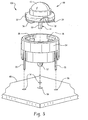
- Figure 8 is an illustration of another embodiment of the system comprising a carrier array and LED packages
- Figure 9 is an exploded view of another embodiment of an LED package with plural LED dice
- Figure 10 is a perspective view of a segmented annular contact according to several embodiments.
- Figure 11 is an exploded view of another embodiment of an LED package with plural LED dice connected in series;
- Figure 12 is a plan view of a leadframe with plural LED dice connected in series according to an embodiment of the present invention.
- Figure 13A is a plan view of an LED package showing an embodiment of the flexible extensions and base contact for connecting electrical power;
- Figure 13B is a plan view of electrical contacts on a PCB or a mounting device that correspond to the flexible extensions and base contact of Figure 13A according to an embodiment of the present invention
- Figure 14A is a plan view of an LED package showing an alternate embodiment of the flexible extensions and base contact for connecting electrical power;
- Figure 14B is a plan view of electrical contacts on a PCB or a mounting device that correspond to the flexible extensions and base contact of Figure 14A according to an embodiment of the present invention
- Figure 15A is a side elevation of another embodiment of an LED package
- Figure 15B is a bottom view of the LED package of Figure 15A according to an embodiment of the present invention.
- Figure 16A is a side elevation of another embodiment of an LED package
- Figure 16B is a bottom view of the LED package of Figure 16A according to an embodiment of the present invention.
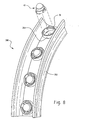
- Figure 17 is an illustration of another embodiment of a system comprising a carrier strip and LED packages.
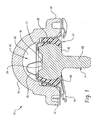
- the LED package 10 comprises an annular contact 12, a base contact, 14, an LED die 16, and a lens 18.
- the annular contact 12 and base contact 14 may each be configured as either an anode or as a cathode for the LED die 16, as desired.
- An optical material 20 may be located in a cavity 22 defined by the annular contact 12, the base contact 14, and the lens 18.
- the optical material 20 may be a silicone material, a gel or grease, a non-resilient material, a non-liquid material, or the like.
- the cavity 22 may contain a liquid, viscous, resilient, rigid or solid optical material 20 or may not contain any material.
- the optical material 20 may be "UV-stable" to resist degradation due to exposure to ultraviolet radiation, such as from sunlight.
- the LED die 16 may be coupled to the annular contact 12 via a wire bonding 26.
- the LED die 16 may also be coupled to a die cup 24 of the base contact 14 by solder or a thermally and electrically conductive adhesive, such as an epoxy.
- the die cup 24 may have reflective surfaces to aid in the distribution of light emitted by the LED die 16.
- a leadframe 27 may be assembled by coupling the base contact 14 to the annular contact 12 through use of a coupling material 28, which may be liquid crystal polymer or the like, so long as the material is thermally conductive and electrically insulating.
- the lens 18 is coupled to the leadframe 27 via complementary coupling devices 30 which may be, for example, barbs or tabs, and coupling devices 31 which may be, for example, receiving openings.
- complementary coupling devices 30 which may be, for example, barbs or tabs
- coupling devices 31 which may be, for example, receiving openings.
- the lens 18 may be coupled to the leadframe 27 with an adhesive, such as an epoxy.
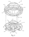
- the lens 18 of the LED package 10 further comprises protrusions 32, which may be lens "feet,” that allow the LED package 10 to be removeably secured in a coupling device 36 of a mounting device 54 in a socket-like fashion, wherein the feet 32 are biased against the coupling device 36 via flexible extensions 34 extending from a peripheral portion of the annular contact 12.
- the flexible extensions 34 may also serve as contacts to electrically couple the annular contact 12 to corresponding contacts in the mounting device 54, or to corresponding lands on a printed circuit board (“PCB”) 40.
- the mounting device 54 extensions 55 extending from the mounting device 54 are received in openings 56 in PCB 40 and extension 57 extending from the mounting device 54 is received in opening 58 in the PCB 40 to couple the mounting device 54 to the PCB 40.
- an opening 59 (not shown) receives the base contact post 60.
- the opening 59 may have a corresponding contact to detachably couple to the base contact post 60 to complete the electrical connection to the LED package 10.
- the annular contact 12 forms a portion of the leadframe 27 for the LED package 10 and is further designed to provide a large surface area for sinking heat generated during use.
- the shape has the still further benefit of reducing thermal expansion due to hoop stresses inherent with the annular geometry.
- the annular contact 12 somewhat resembles an inverted pie pan having a centralized, preferably concentric window 50 formed in the ''bottom'' 52 providing access to the LED die 16 and wire bonding 26, and through which light emitted from the LED die 16 is distributed to the lens 18.
- other embodiments contemplate other generally symmetrical shapes, which are equally well suited as leadframe portions, as is the annular embodiment.
- the stamped barbs 30 are formed about the periphery of a body of the annular contact 12 for captive engagement between the annular contact and the receiving openings 31 of the lens 18 during assembly of the LED package 10.
- the LED package 10 also allows for significant improvement in the assembly process for products that use LEDs. Since the LED package 10 is not orientation-specific, it may be mounted in the mounting device 54 on the PCB 40 as shown in Figures 2 and 5, or as seen in Figure 7 the LED package 10 may be mounted in a mounting device 254 in a light illumination device 200. Likewise, as shown in Figure 8 the LED package 10 may be mounted in a mounting device 354 in an light fixture assembly 300, where in any of these embodiments the LED package 10 is mounted in any orientation, radially about its center. This eliminates the need for specific component orientation prior to assembly.
- FIG. 1-5 and 7-8 may resemble a plug that allows the LED package 10 to be easily installed into the coupling device 36 of the mounting device 54,254,354 in a socket-like fashion without the need for heat or tools, and secured by rotating the LED package 10 until the protrusions 32 are fully engaged with the coupling devices 36.
- the LED package 10 utilize multiple LED dice 16, such as the embodiments shown in Figure 9.
- the dice 16 may be any desired combination of LED colors, such as red, green and blue.
- each of the LED dice 16 may be coupled via wire bonding 26 to different segments of the annular contact 12 to provide two or more separate annular contact segments for each LED die 16.
- An example annular contact 12 having three segments 12A-C is shown in Figures 9 and 10.
- the annular contact also has a centralized, preferably concentric window 50 formed in the "bottom" 52 providing access to the LED die 16 and wire bonding 26, and through which light emitted from the LED die 16 is distributed to the lens 18.
- the segmented annular contact 12 may include flexible extensions 34 and complementary coupling devices 30.
- Annular contact segments 12A-C may be electrically isolated to facilitate individual illumination of LED dice 16. Alternatively, the annular contact segments 12A-C may be electrically interconnected to simultaneously illuminate the LED dice 16. Electrical power may be coupled to multiple LED dice 16 by connecting the N-type material portions or contacts of the dice to the base contact 14 to form a first electrical connection to a power source. Alternatively, the P-type material contact of the dice 16 may be connected to the base contact 14. The remaining contacts of the dice 16 are then individually connected to particular annular contact segments 12A-C.
- two or more LED dice 16 may be electrically insulated from the base contact 14 and electrically interconnected in series fashion, as illustrated in Figures 11 and 12 such that the N-type contact of a first LED die 16 is connected to a P-type contact of a second LED die with a wire bond. Additional LED dice 16 may be connected in the series string in a like manner.
- the P-type contact of the first LED die 16 is connected to the annular contact 12 with a wire bond while the N-type contact of the last LED die in the series is connected to the base contact 14.
- the P-type contact of the first LED die 16 may be connected to the base contact and the N-type contact of the last LED die in the series may be connected to the annular contact 12 with a wire bond.
- the P-type and N-type contacts may be located on the top surface of the die 16 to facilitate the wire bonding connections.
- the flexible extensions 34 may be used to complete the electrical connection to a power source, as previously described. At least one flexible extension 34 may be connected to each LED die 16.
- the flexible extensions 34A-C may be configured to orient with corresponding contacts 64A-C on a PCB 40 or a mounting device 54 to facilitate individual coupling to the LED dice 16 via annular contact segments 12A-C, as shown in Figures 13A-B.
- the orientation of the flexible extensions 34 and corresponding contacts 64 may or may not be indexed.
- the base contact 14 may couple to a corresponding contact 66 to complete the electrical circuit.
- the flexible extensions 34A-C may each have a differing diametrical pitch as shown in Figure 14A to permit individual electrical coupling to corresponding contacts 64A-C, as shown in Figure 14B, allowing individual electrical coupling to the LED dice 16 connected to annular contact segments 12A-C.
- the base contact 14 couples with a corresponding contact 66 to complete the electrical circuit.
- the leadframe 27 may be laser welded, rather than soldered, or otherwise mechanically coupled to the PCB 40 to provide electrical contact between the LED package 10 and the PCB 40, thereby minimizing the risk of overheating the LED die 16 during assembly of the LED package 10 into a product or subassembly.
- the leadframe 27 may be laser welded to a contact arrangement to eliminate the need for a PCB 40.
- the LED package 10 utilizes a lens 18, which may be premolded and may be constructed of any one of a number of known materials, such as epoxy resin, urea resin, silicon resin, acrylic resin, glass, or the like, in various lens patterns or geometries. While shown in a circular embodiment, the shape of the lens 18 may be any generally symmetrical shape such as, without limitation, square, hexagonal, triangular and the like.
- the lens 18 provides the optical pattern for the LED package 10, and may be configured as a convex, concave, or collimating lens and may be optically clear or contain dispersants to diffuse the emitted light.
- the inside surface of the lens 18 may be coated with a suitable light excitable material or the lens 18 may comprise a suitable light excitable material, which may be a phosphor material, for generating white light when excited with a blue, ultraviolet, or other color LED die 16.
- the optical material 20 may comprise the light excitable material.
- the lens 18 both partially defines the cavity 22 for the optical material 20 and acts as a protective shield for the LED die 16 and attendant wire bonding 26. By premolding the lens 18, the optical output of the LED package 10 is easily modified by producing a different configuration, pattern, or geometry of the lens 18.
- the LED die 16 which may have an index of refraction "n" of about 3.40, provides light output.
- the LED die 16 design and its method of manufacture are described in by Shimizu and others.
- the LED die 16 may be a multi-layer epitaxial semiconductor structure comprising an N-type material portion and a P-type material portion wherein the P-type material portion is electrically connected to an annular contact 12 and the N-type material portion is electrically connected to a base contact 14.
- the N-type material portion may be electrically connected to the annular contact 12 and the P-type material portion may be electrically connected to the base contact 14.
- the LED die 16 When electrically energized, the LED die 16 emits light of a wavelength predetermined by its chemical makeup.
- multiple colors of LED dice 16, such as red, blue and green, may be combined into a single LED package, as previously discussed and seen in Figures 9, 11 and 12.
- a blue, ultraviolet, or other color LED die 16 is used to excite a phosphor containing component in the lens 18 or in optical material 20 in order to produce a white light.
- Some prior art devices that have similar functions are Singer et al. that teaches the use of a phosphor layer on top of a blue LED die to produce a white LED, Shimizu et al. that teaches the use of phosphor materials embedded into a resin coating material place over the LED die, and Shimizu et al. that teaches the use of phosphor materials in the molded lens surrounding the LED die.
- the optical material 20 may be an optical quality gel or grease or other soft optical material, which may have a refractive index "n" of about 1.70 or greater.
- the optical material 20 is contained in the lens 18 to possibly provide gradual transition of index of refraction between the LED die 16, which may have an index of refraction "n" of about 3.40, and the lens 18, which may have an index of refraction "n” of about 1.5.
- the optical material 20 is an optical gel it may be of a type manufactured, for example, by Nye Optical.
- the soft optical material 20 reduces the stress on the wire bond 26 and LED die 16 caused by thermal expansion of the LED components.
- the optical material 20 is formed so that it has varying indexes of refraction by arranging it in layers within the lens 18, where the layer having the highest index of refraction is closest to the LED die 16. In addition to facilitating assembly of the LED package 10, the varying layers of optical material 20 between the LED die 16 and the lens 18 also lessens the Fresnel losses within the LED package 10.
- a white emitted light is produced using a blue, ultraviolet, or other color LED die 16 by exciting light excitable materials, which may be fluorescent materials, that may be located in or on the lens 18, or similar to what is disclosed in Shimizu et al. in U.S. Pat. Nos. 5,998,925 and 6,069,440, the optical material 20 may contain a suitable phosphor material.
- the optical material 20 may contain a suitable phosphor material.
- one or more layers of the optical material 20 replaces the prior art cured epoxy coating resin.
- the phosphor bearing optical material 20 fills the entire cavity 22, which is more effective for converting more of the excitation output into white light.
- the semispherical configuration of the phosphor bearing optical material 20 also provides more of an omni-directional output than the LEDs generally depicted by Shimizu et al.
- the wire bonding 26 used to connect the annular contact 12 to the LED die 16 may be gold, but may also be made from copper, platinum, aluminum or alloys thereof.
- the diameter of the wire bonding 26 is typically in the area from 10-45 ⁇ m.
- wire bonds with diameters less than 25 ⁇ m are not recommended because of breakage at the bonding point.
- the wire bonding 26 is encapsulated in a soft optical material rather than a hard resin, thus permitting some expansion without loss of the electrical bonding.
- the wire bonding 26 is connected to the N-type material portion or P-type material portion of the LED die 16 and the annular contact 12 by conventional wire bonding techniques.
- the base contact 14 which may be a copper slug or a heat sink, is provided at the center of the LED package 10 and serves as an electrical connection for the LED package 10.
- the base contact 14 is configured to have the die cup 24 at its uppermost surface, within which the LED die 16 is mounted.
- the liquid crystal polymer 28 may be used to couple the base contact 14 into place within the annular contact 12 to form the leadframe 27.
- the liquid crystal polymer 28 also provides a barrier to seal the optical material 20 in place.
- the liquid crystal polymer 28 is thermally coupled to the annular contact 12 it provides for additional heat sinking for the LED die 16.
- the inner surface of the die cup 24 may be finished with a reflective surface, via plating, polishing or other means, in order to direct the light emitted from the LED die 16 in a predetermined manner.
- the mass of the base contact 14 provides superior heat sinking for the LED die 16 to allow higher power to be applied to the LED die 16, resulting in higher lumen output.
- the base contact 14 may be provided with an integral center post 60, as best illustrated in Figures 1-5.
- the LED package 10 can be assembled into a PCB 40 assembly by normal soldering techniques or, without the use of heat, by fitting the LED package 10 into a complementary socket arrangement of mounting devices 32 and 36.
- a lower base portion 62 of the base contact 14 can be laser welded or otherwise mechanically coupled to the PCB 40 or mounting device 54 to provide an electrical connection.
- an LED package 410 comprises a base contact 414 with a post 460 that comprises protrusions 470 that may be coupled to a complementary coupling device, which may be a bayonet-type coupling device.
- an LED package 510 comprises a base contact 514 with a post 560 having a threaded outer surface 570, which may be coupled to a complementary coupling device. The threaded outer surface 570 may serve to mechanically and/or electrically couple the LED package 510 to the complementary coupling device (not shown).
- one embodiment provides an array of the annular contacts 12 that is formed continuously into the carrier strip 70, which may be an annular contact carrier strip, such as by stamping or other conventional means.
- the anode carrier strip 70 also provides for alternate means of packaging the LED package 10 into subassemblies.
- the carrier strip 42 which may be a base contact carrier strip, containing receiving devices 72 having a common base contact may be employed as one assembly.
- Each of the center posts 60 of each of the LED packages 10 may be connected to the receiving devices 72 on a carrier strip 42, where each of the annular contacts 12 may be connected using a carrier strip 70. In such an application, only one electrical connection to the base contact via the carrier strip 42 would be necessary.
- the annular contact carrier strip 70 can be configured to have a common electrical connection, in which case an entire strip of the LED packages 10 can be easily assembled by making only two electrical connections.
- the base contact carrier strip 42 and the anode carrier strip 70 may be periodically scored (shown as dashed lines) along their length to enable the base contact carrier strip 42 and the annular contact carrier strip 70 to be in broken into predetermined lengths.
- the LED package 10 may be incorporated directly into products to eliminate the need for secondary coupling devices and printed circuit boards.
- Figure 7 illustrates a portable lighting illumination device 200, such as a flashlight.
- the LED package 10 is mounted into a mounting device 254.
- the mounting device 254 serves to mechanically secure the LED package 10 within the flashlight 200, and also facilitates electrical connections between the LED package 10 and the batteries 256.
- a housing 258 and lighthead 260 provide a secure package for the flashlight components.
- the LED package 10 may be directly incorporated to a light fixture 300, as shown in Figure 8.
- a housing structure 302 holds one or more mounting devices 354.
- the mounting devices 354 mechanically secure the LED packages 10 to the housing structure 302 and also facilitate electrical connections to the LED package.
- the light fixture 300 may be any type of interior or exterior, fixed or portable light. Examples include, but are not limited to, position lights, reading lights, indicators, night lights, backlights, and marker lights. Additional examples may include automotive signaling devices such as stop lights, brake lights, taillights indicator lights, turn signals and hazard lights.
Applications Claiming Priority (2)
| Application Number | Priority Date | Filing Date | Title |
|---|---|---|---|
| US411707 | 2003-04-11 | ||
| US10/411,707 US6903380B2 (en) | 2003-04-11 | 2003-04-11 | High power light emitting diode |
Publications (2)
| Publication Number | Publication Date |
|---|---|
| EP1467416A2 true EP1467416A2 (fr) | 2004-10-13 |
| EP1467416A3 EP1467416A3 (fr) | 2010-11-03 |
Family
ID=32869228
Family Applications (1)
| Application Number | Title | Priority Date | Filing Date |
|---|---|---|---|
| EP04005176A Withdrawn EP1467416A3 (fr) | 2003-04-11 | 2004-03-04 | Diode électroluminescente de grande puissance |
Country Status (7)
| Country | Link |
|---|---|
| US (2) | US6903380B2 (fr) |
| EP (1) | EP1467416A3 (fr) |
| CN (1) | CN1536686A (fr) |
| CA (1) | CA2451808A1 (fr) |
| MX (1) | MXPA03012020A (fr) |
| MY (1) | MY134507A (fr) |
| TW (1) | TWI238542B (fr) |
Cited By (19)
| Publication number | Priority date | Publication date | Assignee | Title |
|---|---|---|---|---|
| WO2006047306A1 (fr) * | 2004-10-22 | 2006-05-04 | Johnson Controls Technology Company | Lampe avec un materiau emissif a l'exterieur de la source de lumiere |
| US7235878B2 (en) | 2004-03-18 | 2007-06-26 | Phoseon Technology, Inc. | Direct cooling of LEDs |
| EP1892690A3 (fr) * | 2006-08-21 | 2008-10-08 | Honeywell Technologies Sarl | Affichage muni de LEDS multicolores |
| WO2010004503A1 (fr) * | 2008-07-11 | 2010-01-14 | Koninklijke Philips Electronics N.V. | Dispositif luminescent et procédé d’assemblage |
| WO2010010495A1 (fr) * | 2008-07-25 | 2010-01-28 | Koninklijke Philips Electronics N.V. | Dispositif de refroidissement permettant de refroidir une puce à semi-conducteurs |
| WO2010051985A3 (fr) * | 2008-11-05 | 2010-07-01 | Zumtobel Lighting Gmbh & Co.Kg. | Lampe à led |
| US7819550B2 (en) | 2003-10-31 | 2010-10-26 | Phoseon Technology, Inc. | Collection optics for led array with offset hemispherical or faceted surfaces |
| WO2011053260A1 (fr) * | 2009-10-29 | 2011-05-05 | Pokorny Otto | Luminaire à agencement compact doté d'une ampoule compacte à del comprenant une interface thermique, mécanique et électrique |
| WO2012041639A1 (fr) * | 2010-09-30 | 2012-04-05 | Osram Ag | Lentille moulable à haute température, dispositif d'éclairage comprenant la lentille et procédé de fabrication du dispositif d'éclairage |
| WO2012059364A1 (fr) * | 2010-11-02 | 2012-05-10 | Osram Ag | Dispositif d'éclairage et procédé d'assemblage d'un dispositif d'éclairage |
| US8192053B2 (en) | 2002-05-08 | 2012-06-05 | Phoseon Technology, Inc. | High efficiency solid-state light source and methods of use and manufacture |
| US8637332B2 (en) | 2004-03-18 | 2014-01-28 | Phoseon Technology, Inc. | Micro-reflectors on a substrate for high-density LED array |
| WO2015067613A1 (fr) * | 2013-11-08 | 2015-05-14 | Osram Opto Semiconductors Gmbh | Composant optoélectronique |
| WO2015155619A1 (fr) * | 2014-04-07 | 2015-10-15 | Elica S.P.A. | Hotte domestique |
| US9281001B2 (en) | 2004-11-08 | 2016-03-08 | Phoseon Technology, Inc. | Methods and systems relating to light sources for use in industrial processes |
| EP2060226B1 (fr) * | 2007-11-14 | 2017-01-04 | Carl Zeiss Meditec AG | Endoilluminateur |
| EP3210521A1 (fr) * | 2016-02-24 | 2017-08-30 | Richard Wolf GmbH | Instrument à tige endoscopique |
| US10544943B2 (en) | 2014-04-07 | 2020-01-28 | Elica S.P.A. | Domestic hoods |
| EP3832199A1 (fr) * | 2019-12-06 | 2021-06-09 | Marelli Automotive Lighting Italy S.p.A. | Dispositif d'éclairage et / ou de signalisation automobile et procédé d'assemblage associé |
Families Citing this family (174)
| Publication number | Priority date | Publication date | Assignee | Title |
|---|---|---|---|---|
| DE10117889A1 (de) * | 2001-04-10 | 2002-10-24 | Osram Opto Semiconductors Gmbh | Leiterrahmen und Gehäuse für ein strahlungsemittierendes Bauelement, strahlungsemittierendes Bauelement sowie Verfahren zu dessen Herstellung |
| US8201985B2 (en) | 2001-08-24 | 2012-06-19 | Cao Group, Inc. | Light bulb utilizing a replaceable LED light source |
| US8569785B2 (en) * | 2001-08-24 | 2013-10-29 | Cao Group, Inc. | Semiconductor light source for illuminating a physical space including a 3-dimensional lead frame |
| US7728345B2 (en) * | 2001-08-24 | 2010-06-01 | Cao Group, Inc. | Semiconductor light source for illuminating a physical space including a 3-dimensional lead frame |
| US7976211B2 (en) * | 2001-08-24 | 2011-07-12 | Densen Cao | Light bulb utilizing a replaceable LED light source |
| KR20080064904A (ko) * | 2002-06-14 | 2008-07-09 | 레드니엄 테크놀로지 피티와이 리미티드 | Led 패키징 방법 및 패키징된 led |
| US7244965B2 (en) | 2002-09-04 | 2007-07-17 | Cree Inc, | Power surface mount light emitting die package |
| US7775685B2 (en) * | 2003-05-27 | 2010-08-17 | Cree, Inc. | Power surface mount light emitting die package |
| US6903380B2 (en) * | 2003-04-11 | 2005-06-07 | Weldon Technologies, Inc. | High power light emitting diode |
| US20050006659A1 (en) * | 2003-07-09 | 2005-01-13 | Ng Kee Yean | Light emitting diode utilizing a discrete wavelength-converting layer for color conversion |
| US20050053896A1 (en) * | 2003-09-09 | 2005-03-10 | The Procter & Gamble Company | Illuminated electric toothbrushes emitting high luminous intensity toothbrush |
| FR2862424B1 (fr) * | 2003-11-18 | 2006-10-20 | Valeo Electronique Sys Liaison | Dispositif de refroidissement d'un composant electrique et procede de fabrication de ce dispositif |
| US7321161B2 (en) * | 2003-12-19 | 2008-01-22 | Philips Lumileds Lighting Company, Llc | LED package assembly with datum reference feature |
| US7081644B2 (en) * | 2004-02-06 | 2006-07-25 | Barnes Group Inc. | Overmolded lens on leadframe and method for overmolding lens on lead frame |
| KR100576866B1 (ko) * | 2004-06-16 | 2006-05-10 | 삼성전기주식회사 | 발광다이오드 및 그 제조방법 |
| JP2006049657A (ja) * | 2004-08-06 | 2006-02-16 | Citizen Electronics Co Ltd | Ledランプ |
| US7670872B2 (en) * | 2004-10-29 | 2010-03-02 | LED Engin, Inc. (Cayman) | Method of manufacturing ceramic LED packages |
| US8816369B2 (en) | 2004-10-29 | 2014-08-26 | Led Engin, Inc. | LED packages with mushroom shaped lenses and methods of manufacturing LED light-emitting devices |
| US9929326B2 (en) | 2004-10-29 | 2018-03-27 | Ledengin, Inc. | LED package having mushroom-shaped lens with volume diffuser |
| US7473933B2 (en) * | 2004-10-29 | 2009-01-06 | Ledengin, Inc. (Cayman) | High power LED package with universal bonding pads and interconnect arrangement |
| US8324641B2 (en) | 2007-06-29 | 2012-12-04 | Ledengin, Inc. | Matrix material including an embedded dispersion of beads for a light-emitting device |
| US7772609B2 (en) * | 2004-10-29 | 2010-08-10 | Ledengin, Inc. (Cayman) | LED package with structure and materials for high heat dissipation |
| US8134292B2 (en) * | 2004-10-29 | 2012-03-13 | Ledengin, Inc. | Light emitting device with a thermal insulating and refractive index matching material |
| KR100631903B1 (ko) * | 2005-02-17 | 2006-10-11 | 삼성전기주식회사 | 고출력 led 하우징 및 그 제조 방법 |
| DE102005020908A1 (de) * | 2005-02-28 | 2006-08-31 | Osram Opto Semiconductors Gmbh | Beleuchtungsvorrichtung |
| US20080296589A1 (en) * | 2005-03-24 | 2008-12-04 | Ingo Speier | Solid-State Lighting Device Package |
| CA2614803C (fr) * | 2005-04-05 | 2015-08-25 | Tir Technology Lp | Boitier de dispositif electronique a evaporateur integre |
| JP2006324324A (ja) * | 2005-05-17 | 2006-11-30 | Sumitomo Electric Ind Ltd | 発光装置、発光装置の製造方法および窒化物半導体基板 |
| KR100616684B1 (ko) * | 2005-06-03 | 2006-08-28 | 삼성전기주식회사 | 고출력 led 패키지 및 그 제조방법 |
| US7980743B2 (en) * | 2005-06-14 | 2011-07-19 | Cree, Inc. | LED backlighting for displays |
| CN100538421C (zh) * | 2005-06-14 | 2009-09-09 | 罗姆股份有限公司 | 发光装置 |
| KR100592508B1 (ko) * | 2005-07-15 | 2006-06-26 | 한국광기술원 | 비콘 모양의 기판을 구비한 고출력 발광 다이오드 패키지 |
| US7234842B2 (en) * | 2005-07-28 | 2007-06-26 | Tom Frederico | Replaceable LED socket torch and lighting head assembly |
| TWI297784B (en) * | 2005-09-22 | 2008-06-11 | Lite On Technology Corp | Optical module having a lens formed without contacting a reflector and method of manufacturing the same |
| KR20070045462A (ko) * | 2005-10-27 | 2007-05-02 | 엘지이노텍 주식회사 | 발광 다이오드 패키지 |
| US20070096132A1 (en) * | 2005-11-01 | 2007-05-03 | Jiahn-Chang Wu | Coaxial LED lighting board |
| JP2009516913A (ja) * | 2005-11-22 | 2009-04-23 | コーニンクレッカ フィリップス エレクトロニクス エヌ ヴィ | 発光モジュール及びその製造方法 |
| SG151282A1 (en) * | 2005-12-29 | 2009-04-30 | Lam Chiang Lim | High power led housing removably fixed to a heat sink |
| US8044412B2 (en) | 2006-01-20 | 2011-10-25 | Taiwan Semiconductor Manufacturing Company, Ltd | Package for a light emitting element |
| TW200729539A (en) * | 2006-01-26 | 2007-08-01 | Litmx Inc | Making method for the circuit board of separated light emitting diode |
| JP2007235103A (ja) * | 2006-01-31 | 2007-09-13 | Sanyo Electric Co Ltd | 半導体発光装置 |
| JP5130680B2 (ja) * | 2006-03-02 | 2013-01-30 | 日亜化学工業株式会社 | 半導体装置およびその形成方法 |
| US20070230182A1 (en) * | 2006-03-28 | 2007-10-04 | Yun Tai | Led module |
| FR2899763B1 (fr) * | 2006-04-06 | 2008-07-04 | Valeo Electronique Sys Liaison | Support, notamment pour composant electronique de puissance, module de puissance comprenant ce support, ensemble comprenant le module et organe electrique pilote par ce module |
| TWI297223B (en) * | 2006-04-25 | 2008-05-21 | Gigno Technology Co Ltd | Package module of light emitting diode |
| BRPI0711150A2 (pt) | 2006-05-02 | 2011-08-23 | Superbulbs Inc | bulbo de led de plástico |
| AU2007248758A1 (en) | 2006-05-02 | 2007-11-15 | Daniel Chandler | Heat removal design for LED bulbs |
| EP2013919A2 (fr) | 2006-05-02 | 2009-01-14 | Superbulbs, Inc. | Procédé de dispersion lumineuse et diffusions préférentielles de certaines longueurs d'onde de lumière destinées à des diodes électroluminescentes et à des ampoules construites à partir de ce procédé |
| US7906794B2 (en) | 2006-07-05 | 2011-03-15 | Koninklijke Philips Electronics N.V. | Light emitting device package with frame and optically transmissive element |
| US20080029720A1 (en) | 2006-08-03 | 2008-02-07 | Intematix Corporation | LED lighting arrangement including light emitting phosphor |
| WO2008052327A1 (fr) * | 2006-10-31 | 2008-05-08 | Tir Technology Lp | Ensemble d'éclairage |
| US7587289B1 (en) * | 2007-02-13 | 2009-09-08 | American Megatrends, Inc. | Data cable powered sensor fixture |
| US8011794B1 (en) | 2007-02-13 | 2011-09-06 | American Megatrends, Inc. | Data cable powered light fixture |
| US20080197374A1 (en) * | 2007-02-15 | 2008-08-21 | Wen-Kung Sung | High-power light-emitting diode |
| US20080218998A1 (en) * | 2007-03-08 | 2008-09-11 | Quest William J | Device having multiple light sources and methods of use |
| US20080291674A1 (en) * | 2007-04-06 | 2008-11-27 | Welsh Jr Calvin Rex | Lighting device utilizing an LED light source for projection of a light pattern onto a surface |
| US7540761B2 (en) * | 2007-05-01 | 2009-06-02 | Tyco Electronics Corporation | LED connector assembly with heat sink |
| WO2008151009A1 (fr) * | 2007-05-31 | 2008-12-11 | Lumination Llc | Dispositifs d'éclairage robustes sur le plan environnemental et procédés de fabrication de ceux-ci |
| DE102007025749A1 (de) * | 2007-06-01 | 2008-12-11 | Wacker Chemie Ag | Leuchtkörper-Silicon-Formteil |
| JP5431688B2 (ja) * | 2007-06-29 | 2014-03-05 | ソウル セミコンダクター カンパニー リミテッド | マルチledパッケージ |
| TW200903834A (en) * | 2007-07-05 | 2009-01-16 | Bright Led Electronics Corp | High heat-dissipation light emitting diode device |
| US20090008662A1 (en) * | 2007-07-05 | 2009-01-08 | Ian Ashdown | Lighting device package |
| DE102007036226A1 (de) * | 2007-08-02 | 2009-02-05 | Perkinelmer Elcos Gmbh | Anbringungsstruktur für LEDs, LED-Baugruppe, LED-Baugruppensockel, Verfahren zum Ausbilden einer Anbringungsstruktur |
| US7652301B2 (en) * | 2007-08-16 | 2010-01-26 | Philips Lumileds Lighting Company, Llc | Optical element coupled to low profile side emitting LED |
| CN101162816B (zh) * | 2007-09-13 | 2010-09-01 | 番禺得意精密电子工业有限公司 | 电连接装置 |
| CA2700376C (fr) | 2007-09-21 | 2015-07-21 | Cooper Technologies Company | Dispositif d'eclairage encastre a diodes electroluminescentes |
| WO2009045438A1 (fr) | 2007-10-03 | 2009-04-09 | Superbulbs, Inc. | Ampoules a del en verre |
| EP2215403A4 (fr) | 2007-10-24 | 2012-08-29 | Switch Bulb Co Inc | Diffuseur pour sources lumineuses de diodes électroluminescentes |
| JP5104385B2 (ja) * | 2008-02-20 | 2012-12-19 | 豊田合成株式会社 | Ledランプモジュール |
| US7866850B2 (en) | 2008-02-26 | 2011-01-11 | Journée Lighting, Inc. | Light fixture assembly and LED assembly |
| US7942563B2 (en) * | 2008-02-29 | 2011-05-17 | Tyco Electronics Corporation | LED with light pipe assembly |
| TW200939412A (en) * | 2008-03-14 | 2009-09-16 | Sung Jung Minute Industry Co Ltd | Reinforced chip packaging structure |
| US8158999B2 (en) * | 2008-03-14 | 2012-04-17 | Sung Jung Minute Industry Co., Ltd. | Reinforced chip package structure |
| US20090273940A1 (en) * | 2008-05-01 | 2009-11-05 | Cao Group, Inc. | LED lighting device |
| TWI340219B (en) * | 2008-05-09 | 2011-04-11 | Neobulb Technologies Inc | Outdoor illuminating apparatus |
| JP5155890B2 (ja) | 2008-06-12 | 2013-03-06 | ルネサスエレクトロニクス株式会社 | 半導体装置およびその製造方法 |
| KR101101134B1 (ko) * | 2008-07-03 | 2012-01-05 | 삼성엘이디 주식회사 | Led 패키지 및 그 led 패키지를 포함하는 백라이트 유닛 |
| US8492179B2 (en) * | 2008-07-11 | 2013-07-23 | Koninklijke Philips N.V. | Method of mounting a LED module to a heat sink |
| JP2010034287A (ja) * | 2008-07-29 | 2010-02-12 | Sumitomo Electric Ind Ltd | キャップ及び光モジュール |
| US20100033964A1 (en) * | 2008-08-08 | 2010-02-11 | Photonics & Co., Limited | Light emitting diode (led) lighting device |
| US20100053978A1 (en) * | 2008-08-26 | 2010-03-04 | Han-Ming Lee | Radiating semi-conductor light |
| TR200806540A2 (tr) * | 2008-09-01 | 2010-01-21 | Atalay Suav | Fırınlarda kullanılan bayonet kilitlemeli lamba duyu |
| US20100058837A1 (en) * | 2008-09-05 | 2010-03-11 | Quest William J | Device having multiple light sources and methods of use |
| US20100067240A1 (en) * | 2008-09-16 | 2010-03-18 | John Selverian | Optical Cup For Lighting Module |
| US8188486B2 (en) * | 2008-09-16 | 2012-05-29 | Osram Sylvania Inc. | Optical disk for lighting module |
| US8183585B2 (en) * | 2008-09-16 | 2012-05-22 | Osram Sylvania Inc. | Lighting module |
| US7952114B2 (en) | 2008-09-23 | 2011-05-31 | Tyco Electronics Corporation | LED interconnect assembly |
| JP5227135B2 (ja) * | 2008-10-10 | 2013-07-03 | スタンレー電気株式会社 | 半導体発光装置およびその製造方法 |
| RU2524400C2 (ru) * | 2008-10-14 | 2014-07-27 | Конинклейке Филипс Электроникс Н.В. | Система для передачи тепла между двумя соединяемыми элементами |
| US8075165B2 (en) * | 2008-10-14 | 2011-12-13 | Ledengin, Inc. | Total internal reflection lens and mechanical retention and locating device |
| TW201022327A (en) * | 2008-10-30 | 2010-06-16 | Solvay Advanced Polymers Llc | Hydroquinone-containing polyesters having improved whiteness |
| US20100117106A1 (en) * | 2008-11-07 | 2010-05-13 | Ledengin, Inc. | Led with light-conversion layer |
| TWI391021B (zh) * | 2008-12-22 | 2013-03-21 | Young Optics Inc | 發光二極體封裝體及投影裝置 |
| US8507300B2 (en) * | 2008-12-24 | 2013-08-13 | Ledengin, Inc. | Light-emitting diode with light-conversion layer |
| EP2399070B1 (fr) * | 2009-02-17 | 2017-08-23 | Epistar Corporation | Ampoules d'éclairage à led pour éclairage d'espace |
| US8269248B2 (en) * | 2009-03-02 | 2012-09-18 | Thompson Joseph B | Light emitting assemblies and portions thereof |
| US20100225215A1 (en) * | 2009-03-03 | 2010-09-09 | Han-Ming Lee | Multi-chip cup semi-conductor lamp |
| CN102341646A (zh) | 2009-03-05 | 2012-02-01 | 欧司朗股份有限公司 | 具有插座和容座的发光装置 |
| CN101894901B (zh) | 2009-04-08 | 2013-11-20 | 硅谷光擎 | 用于多个发光二极管的封装 |
| US8598793B2 (en) | 2011-05-12 | 2013-12-03 | Ledengin, Inc. | Tuning of emitter with multiple LEDs to a single color bin |
| US7985000B2 (en) * | 2009-04-08 | 2011-07-26 | Ledengin, Inc. | Lighting apparatus having multiple light-emitting diodes with individual light-conversion layers |
| DE102009022255A1 (de) * | 2009-05-20 | 2010-11-25 | Eutegra Ag | Leuchtdiode mit Kühlkörper |
| KR20110002892A (ko) * | 2009-06-29 | 2011-01-11 | 서울반도체 주식회사 | 발광 모듈 |
| US8622579B2 (en) | 2009-06-29 | 2014-01-07 | Seoul Semiconductor Co., Ltd. | Illumination system |
| CN101988679A (zh) * | 2009-07-29 | 2011-03-23 | 富准精密工业(深圳)有限公司 | 发光二极管模组 |
| DE102009035515A1 (de) * | 2009-07-31 | 2011-02-03 | Osram Gesellschaft mit beschränkter Haftung | Leuchtvorrichtung und Verfahren zum Herstellen einer Leucht-vorrichtung |
| US8414178B2 (en) * | 2009-08-12 | 2013-04-09 | Journée Lighting, Inc. | LED light module for use in a lighting assembly |
| US9029814B2 (en) * | 2009-10-15 | 2015-05-12 | Hamamatsu Photonics K.K. | LED light source device |
| US8303141B2 (en) * | 2009-12-17 | 2012-11-06 | Ledengin, Inc. | Total internal reflection lens with integrated lamp cover |
| CN101764190A (zh) * | 2010-01-01 | 2010-06-30 | 中山伟强科技有限公司 | 一种发光二极管的封装结构 |
| US9080729B2 (en) | 2010-04-08 | 2015-07-14 | Ledengin, Inc. | Multiple-LED emitter for A-19 lamps |
| US9345095B2 (en) | 2010-04-08 | 2016-05-17 | Ledengin, Inc. | Tunable multi-LED emitter module |
| US8858022B2 (en) | 2011-05-05 | 2014-10-14 | Ledengin, Inc. | Spot TIR lens system for small high-power emitter |
| US8193557B2 (en) * | 2010-04-20 | 2012-06-05 | Bridgelux, Inc. | Sub-assembly for a light-emitting device package and a light emitting diode package with features preventing encapsulant delamination |
| WO2011137355A1 (fr) * | 2010-04-30 | 2011-11-03 | Uniflux Led, Inc. | Structure de refroidissement pour lampes à del |
| US8766112B2 (en) * | 2010-07-19 | 2014-07-01 | Robert Bosch Gmbh | Occupant weight sensing using intelligent fastener and vertical load transmitting brackets |
| US9546765B2 (en) | 2010-10-05 | 2017-01-17 | Intematix Corporation | Diffuser component having scattering particles |
| US8957585B2 (en) | 2010-10-05 | 2015-02-17 | Intermatix Corporation | Solid-state light emitting devices with photoluminescence wavelength conversion |
| JP6069205B2 (ja) | 2010-10-05 | 2017-02-01 | インテマティックス・コーポレーションIntematix Corporation | フォトルミネッセンス波長変換を備える発光装置及び波長変換コンポーネント |
| US8610341B2 (en) | 2010-10-05 | 2013-12-17 | Intematix Corporation | Wavelength conversion component |
| US8614539B2 (en) | 2010-10-05 | 2013-12-24 | Intematix Corporation | Wavelength conversion component with scattering particles |
| US8604678B2 (en) | 2010-10-05 | 2013-12-10 | Intematix Corporation | Wavelength conversion component with a diffusing layer |
| TWI414714B (zh) | 2011-04-15 | 2013-11-11 | Lextar Electronics Corp | 發光二極體杯燈 |
| CN102588762A (zh) * | 2011-01-06 | 2012-07-18 | 隆达电子股份有限公司 | 发光二极管杯灯 |
| US8922108B2 (en) | 2011-03-01 | 2014-12-30 | Cree, Inc. | Remote component devices, systems, and methods for use with light emitting devices |
| US9010956B1 (en) | 2011-03-15 | 2015-04-21 | Cooper Technologies Company | LED module with on-board reflector-baffle-trim ring |
| US8513900B2 (en) | 2011-05-12 | 2013-08-20 | Ledengin, Inc. | Apparatus for tuning of emitter with multiple LEDs to a single color bin |
| CN102255032A (zh) * | 2011-07-06 | 2011-11-23 | 深圳市顶点照明设备有限公司 | 一种大功率led的配光结构 |
| US8591069B2 (en) | 2011-09-21 | 2013-11-26 | Switch Bulb Company, Inc. | LED light bulb with controlled color distribution using quantum dots |
| DE102011115037A1 (de) * | 2011-10-07 | 2013-04-11 | NORKA Norddeutsche Kunststoff- und Elektro-Gesellschaft Stäcker mbH & Co. KG | Leuchte mit einem LED-Leuchtmittel |
| US11032884B2 (en) | 2012-03-02 | 2021-06-08 | Ledengin, Inc. | Method for making tunable multi-led emitter module |
| US9897284B2 (en) | 2012-03-28 | 2018-02-20 | Ledengin, Inc. | LED-based MR16 replacement lamp |
| US20140185269A1 (en) | 2012-12-28 | 2014-07-03 | Intermatix Corporation | Solid-state lamps utilizing photoluminescence wavelength conversion components |
| DE102013201808A1 (de) * | 2013-02-05 | 2014-08-07 | Richard Wolf Gmbh | LED-Beleuchtungsmodul |
| US9565782B2 (en) | 2013-02-15 | 2017-02-07 | Ecosense Lighting Inc. | Field replaceable power supply cartridge |
| US9234801B2 (en) | 2013-03-15 | 2016-01-12 | Ledengin, Inc. | Manufacturing method for LED emitter with high color consistency |
| CN105121951A (zh) | 2013-03-15 | 2015-12-02 | 英特曼帝克司公司 | 光致发光波长转换组件 |
| US10033464B2 (en) * | 2013-05-28 | 2018-07-24 | Stmicroelectronics S.R.L. | Optoelectronic device having improved optical coupling |
| DE102013106688B4 (de) * | 2013-06-26 | 2017-08-24 | Osram Oled Gmbh | Optoelektronisches Bauelement und Verfahren zum Herstellen eines optoelektronischen Bauelementes |
| EP2851612B1 (fr) * | 2013-09-24 | 2019-06-26 | Glashütte Limburg Leuchten GmbH + Co. KG | Lampe dotée d'un abat-jour |
| US9327643B2 (en) | 2013-11-21 | 2016-05-03 | Ford Global Technologies, Llc | Photoluminescent lift gate lamp |
| US9406654B2 (en) | 2014-01-27 | 2016-08-02 | Ledengin, Inc. | Package for high-power LED devices |
| US10145529B2 (en) * | 2014-05-30 | 2018-12-04 | Lumileds Llc | Optical lens package for automotive lighting application |
| DE102014107964A1 (de) * | 2014-06-05 | 2015-12-17 | Osram Opto Semiconductors Gmbh | Optoelektronisches Bauelement |
| US10477636B1 (en) | 2014-10-28 | 2019-11-12 | Ecosense Lighting Inc. | Lighting systems having multiple light sources |
| US9642206B2 (en) | 2014-11-26 | 2017-05-02 | Ledengin, Inc. | Compact emitter for warm dimming and color tunable lamp |
| EP3238278B1 (fr) * | 2014-12-22 | 2020-03-04 | MAG Instrument, Inc. | Appareil d'éclairage à efficacité améliorée pourvu d'une del montée directement sur un dissipateur thermique |
| US11306897B2 (en) | 2015-02-09 | 2022-04-19 | Ecosense Lighting Inc. | Lighting systems generating partially-collimated light emissions |
| US9869450B2 (en) | 2015-02-09 | 2018-01-16 | Ecosense Lighting Inc. | Lighting systems having a truncated parabolic- or hyperbolic-conical light reflector, or a total internal reflection lens; and having another light reflector |
| US9530943B2 (en) | 2015-02-27 | 2016-12-27 | Ledengin, Inc. | LED emitter packages with high CRI |
| US9651216B2 (en) | 2015-03-03 | 2017-05-16 | Ecosense Lighting Inc. | Lighting systems including asymmetric lens modules for selectable light distribution |
| US9568665B2 (en) | 2015-03-03 | 2017-02-14 | Ecosense Lighting Inc. | Lighting systems including lens modules for selectable light distribution |
| US9651227B2 (en) | 2015-03-03 | 2017-05-16 | Ecosense Lighting Inc. | Low-profile lighting system having pivotable lighting enclosure |
| US9746159B1 (en) | 2015-03-03 | 2017-08-29 | Ecosense Lighting Inc. | Lighting system having a sealing system |
| DE102015205354A1 (de) * | 2015-03-24 | 2016-09-29 | Osram Gmbh | Optoelektronische Baugruppe und Verfahren zum Herstellen einer optoelektronischen Baugruppe |
| USD785218S1 (en) | 2015-07-06 | 2017-04-25 | Ecosense Lighting Inc. | LED luminaire having a mounting system |
| USD782094S1 (en) | 2015-07-20 | 2017-03-21 | Ecosense Lighting Inc. | LED luminaire having a mounting system |
| USD782093S1 (en) | 2015-07-20 | 2017-03-21 | Ecosense Lighting Inc. | LED luminaire having a mounting system |
| US9651232B1 (en) | 2015-08-03 | 2017-05-16 | Ecosense Lighting Inc. | Lighting system having a mounting device |
| GB2547655A (en) * | 2016-02-23 | 2017-08-30 | Plumen Ltd | A light unit |
| DE102016207947A1 (de) * | 2016-05-09 | 2017-11-09 | Osram Gmbh | Optoelektronische Baugruppe, elektronische Baugruppe, Verfahren zum Ausbilden einer optoelektronischen Baugruppe und Verfahren zum Ausbilden einer elektronischen Baugruppe |
| CA3036345C (fr) * | 2016-09-09 | 2023-12-12 | Photoscience Japan Corporation | Dispositif et procede d'irradiation ultraviolette |
| JP6755772B2 (ja) * | 2016-10-27 | 2020-09-16 | メタウォーター株式会社 | 水処理装置 |
| US10219345B2 (en) | 2016-11-10 | 2019-02-26 | Ledengin, Inc. | Tunable LED emitter with continuous spectrum |
| DE102017100165A1 (de) | 2017-01-05 | 2018-07-05 | Jabil Optics Germany GmbH | Lichtemittierende Anordnung und lichtemittierendes System |
| DE102017105817A1 (de) | 2017-03-17 | 2018-09-20 | First Sensor Lewicki GmbH | Beleuchtungseinrichtung zur Befestigung in einem optischen Diagnosegerät |
| CN106989317B (zh) * | 2017-03-23 | 2023-08-11 | 厦门佰明光电股份有限公司 | 一种透镜及led警示灯 |
| US10088122B1 (en) * | 2017-08-04 | 2018-10-02 | Jute Industrial Co., Ltd. | Integrated lamp |
| CN107370481B (zh) * | 2017-08-22 | 2023-07-21 | 无锡华普微电子有限公司 | 带触摸功能的人体红外感应开关 |
| CN108361563A (zh) * | 2018-02-23 | 2018-08-03 | 芜湖乐知智能科技有限公司 | 一种封装led发光装置 |
| US10575374B2 (en) | 2018-03-09 | 2020-02-25 | Ledengin, Inc. | Package for flip-chip LEDs with close spacing of LED chips |
| CN111370555B (zh) * | 2020-04-07 | 2021-04-30 | 一诠科技(中国)有限公司 | 一种发光二极管 |
| CN113623550B (zh) * | 2021-08-19 | 2023-03-03 | 深圳市雷兴阳实业有限公司 | 球头模顶灯珠、应用该灯珠的装置及应用该灯珠的设备 |
| CN116435201B (zh) * | 2023-06-12 | 2023-09-12 | 四川遂宁市利普芯微电子有限公司 | 一种塑封封装方法以及器件封装结构 |
Citations (4)
| Publication number | Priority date | Publication date | Assignee | Title |
|---|---|---|---|---|
| US5513082A (en) * | 1994-12-16 | 1996-04-30 | Oshino Electric Lamp Works, Ltd. | Small lamp socket device for panel/printed board |
| GB2343549A (en) * | 1998-11-06 | 2000-05-10 | Hewlett Packard Co | LED with silicone encapsulation |
| EP1139439A1 (fr) * | 2000-03-31 | 2001-10-04 | Relume Corporation | DEL avec dissipateur thermique intégré |
| US20020113244A1 (en) * | 2001-02-22 | 2002-08-22 | Barnett Thomas J. | High power LED |
Family Cites Families (28)
| Publication number | Priority date | Publication date | Assignee | Title |
|---|---|---|---|---|
| US3760237A (en) | 1972-06-21 | 1973-09-18 | Gen Electric | Solid state lamp assembly having conical light director |
| US4478588A (en) | 1978-03-06 | 1984-10-23 | Amp Incorporated | Light emitting diode assembly |
| NL8502025A (nl) | 1985-07-15 | 1987-02-02 | Philips Nv | Lagedrukkwikdampontladingslamp. |
| US4882617A (en) | 1986-12-24 | 1989-11-21 | U.S. Philips Corporation | Projection device and associated electro-optic monochrome display device with phosphor layer and interference filters |
| US5266817A (en) * | 1992-05-18 | 1993-11-30 | Lin Paul Y S | Package structure of multi-chip light emitting diode |
| US5578839A (en) | 1992-11-20 | 1996-11-26 | Nichia Chemical Industries, Ltd. | Light-emitting gallium nitride-based compound semiconductor device |
| EP1450415A3 (fr) | 1993-04-28 | 2005-05-04 | Nichia Corporation | Dispositif semi-conducteur composé III-V comprenant des composés à base de nitrure de gallium |
| JP2894921B2 (ja) | 1993-04-30 | 1999-05-24 | シャープ株式会社 | 半導体装置およびその製造方法 |
| US5514627A (en) | 1994-01-24 | 1996-05-07 | Hewlett-Packard Company | Method and apparatus for improving the performance of light emitting diodes |
| JPH07297479A (ja) | 1994-04-27 | 1995-11-10 | Mitsubishi Electric Corp | 光半導体装置およびその製造方法 |
| US5557115A (en) | 1994-08-11 | 1996-09-17 | Rohm Co. Ltd. | Light emitting semiconductor device with sub-mount |
| JP3271645B2 (ja) | 1995-06-08 | 2002-04-02 | 日亜化学工業株式会社 | 窒化物半導体発光ダイオード |
| US5798537A (en) | 1995-08-31 | 1998-08-25 | Kabushiki Kaisha Toshiba | Blue light-emitting device |
| TW383508B (en) | 1996-07-29 | 2000-03-01 | Nichia Kagaku Kogyo Kk | Light emitting device and display |
| JPH11103097A (ja) | 1997-07-30 | 1999-04-13 | Rohm Co Ltd | 半導体発光素子 |
| US5910661A (en) | 1997-05-13 | 1999-06-08 | Colvin, Jr.; Arthur E. | Flourescence sensing device |
| US5813753A (en) | 1997-05-27 | 1998-09-29 | Philips Electronics North America Corporation | UV/blue led-phosphor device with efficient conversion of UV/blues light to visible light |
| US5813752A (en) | 1997-05-27 | 1998-09-29 | Philips Electronics North America Corporation | UV/blue LED-phosphor device with short wave pass, long wave pass band pass and peroit filters |
| US5847507A (en) | 1997-07-14 | 1998-12-08 | Hewlett-Packard Company | Fluorescent dye added to epoxy of light emitting diode lens |
| JPH11135838A (ja) | 1997-10-20 | 1999-05-21 | Ind Technol Res Inst | 白色発光ダイオード及びその製造方法 |
| US6051849A (en) | 1998-02-27 | 2000-04-18 | North Carolina State University | Gallium nitride semiconductor structures including a lateral gallium nitride layer that extends from an underlying gallium nitride layer |
| US6158882A (en) | 1998-06-30 | 2000-12-12 | Emteq, Inc. | LED semiconductor lighting system |
| US6274924B1 (en) | 1998-11-05 | 2001-08-14 | Lumileds Lighting, U.S. Llc | Surface mountable LED package |
| JP2001036143A (ja) | 1999-07-19 | 2001-02-09 | Stanley Electric Co Ltd | マイクロレンズ付発光素子アレイチップ及びその製造方法 |
| US6614103B1 (en) * | 2000-09-01 | 2003-09-02 | General Electric Company | Plastic packaging of LED arrays |
| US6561680B1 (en) * | 2000-11-14 | 2003-05-13 | Kelvin Shih | Light emitting diode with thermally conductive structure |
| US6917057B2 (en) * | 2002-12-31 | 2005-07-12 | Gelcore Llc | Layered phosphor coatings for LED devices |
| US6903380B2 (en) * | 2003-04-11 | 2005-06-07 | Weldon Technologies, Inc. | High power light emitting diode |
-
2003
- 2003-04-11 US US10/411,707 patent/US6903380B2/en not_active Expired - Lifetime
- 2003-05-16 MY MYPI20031826A patent/MY134507A/en unknown
- 2003-05-28 TW TW092114322A patent/TWI238542B/zh not_active IP Right Cessation
- 2003-12-02 CA CA002451808A patent/CA2451808A1/fr not_active Abandoned
- 2003-12-19 MX MXPA03012020A patent/MXPA03012020A/es active IP Right Grant
-
2004
- 2004-02-03 CN CNA2004100032865A patent/CN1536686A/zh active Pending
- 2004-03-04 EP EP04005176A patent/EP1467416A3/fr not_active Withdrawn
-
2005
- 2005-04-26 US US11/114,991 patent/US7138667B2/en active Active
Patent Citations (5)
| Publication number | Priority date | Publication date | Assignee | Title |
|---|---|---|---|---|
| US5513082A (en) * | 1994-12-16 | 1996-04-30 | Oshino Electric Lamp Works, Ltd. | Small lamp socket device for panel/printed board |
| GB2343549A (en) * | 1998-11-06 | 2000-05-10 | Hewlett Packard Co | LED with silicone encapsulation |
| EP1139439A1 (fr) * | 2000-03-31 | 2001-10-04 | Relume Corporation | DEL avec dissipateur thermique intégré |
| US20020113244A1 (en) * | 2001-02-22 | 2002-08-22 | Barnett Thomas J. | High power LED |
| WO2002069409A1 (fr) * | 2001-02-22 | 2002-09-06 | Weldon Technologies, Inc. | Diode electroluminescente grande puissance |
Cited By (26)
| Publication number | Priority date | Publication date | Assignee | Title |
|---|---|---|---|---|
| US8192053B2 (en) | 2002-05-08 | 2012-06-05 | Phoseon Technology, Inc. | High efficiency solid-state light source and methods of use and manufacture |
| US10401012B2 (en) | 2002-05-08 | 2019-09-03 | Phoseon Technology, Inc. | High efficiency solid-state light source and methods of use and manufacture |
| US8496356B2 (en) | 2002-05-08 | 2013-07-30 | Phoseon Technology, Inc. | High efficiency solid-state light source and methods of use and manufacture |
| US8523387B2 (en) | 2003-10-31 | 2013-09-03 | Phoseon Technology, Inc. | Collection optics for LED array with offset hemispherical or faceted surfaces |
| US7819550B2 (en) | 2003-10-31 | 2010-10-26 | Phoseon Technology, Inc. | Collection optics for led array with offset hemispherical or faceted surfaces |
| US7235878B2 (en) | 2004-03-18 | 2007-06-26 | Phoseon Technology, Inc. | Direct cooling of LEDs |
| US8637332B2 (en) | 2004-03-18 | 2014-01-28 | Phoseon Technology, Inc. | Micro-reflectors on a substrate for high-density LED array |
| WO2006047306A1 (fr) * | 2004-10-22 | 2006-05-04 | Johnson Controls Technology Company | Lampe avec un materiau emissif a l'exterieur de la source de lumiere |
| US9281001B2 (en) | 2004-11-08 | 2016-03-08 | Phoseon Technology, Inc. | Methods and systems relating to light sources for use in industrial processes |
| EP1892690A3 (fr) * | 2006-08-21 | 2008-10-08 | Honeywell Technologies Sarl | Affichage muni de LEDS multicolores |
| EP2060226B1 (fr) * | 2007-11-14 | 2017-01-04 | Carl Zeiss Meditec AG | Endoilluminateur |
| WO2010004503A1 (fr) * | 2008-07-11 | 2010-01-14 | Koninklijke Philips Electronics N.V. | Dispositif luminescent et procédé d’assemblage |
| US8559175B2 (en) | 2008-07-25 | 2013-10-15 | Koninlijke Philips N.V. | Cooling device for cooling a semiconductor die |
| WO2010010495A1 (fr) * | 2008-07-25 | 2010-01-28 | Koninklijke Philips Electronics N.V. | Dispositif de refroidissement permettant de refroidir une puce à semi-conducteurs |
| WO2010051985A3 (fr) * | 2008-11-05 | 2010-07-01 | Zumtobel Lighting Gmbh & Co.Kg. | Lampe à led |
| WO2011053260A1 (fr) * | 2009-10-29 | 2011-05-05 | Pokorny Otto | Luminaire à agencement compact doté d'une ampoule compacte à del comprenant une interface thermique, mécanique et électrique |
| WO2012041639A1 (fr) * | 2010-09-30 | 2012-04-05 | Osram Ag | Lentille moulable à haute température, dispositif d'éclairage comprenant la lentille et procédé de fabrication du dispositif d'éclairage |
| US9447943B2 (en) | 2010-09-30 | 2016-09-20 | Osram Gmbh | High temperature moldable lens, lighting device comprising lens and method making lighting device |
| WO2012059364A1 (fr) * | 2010-11-02 | 2012-05-10 | Osram Ag | Dispositif d'éclairage et procédé d'assemblage d'un dispositif d'éclairage |
| WO2015067613A1 (fr) * | 2013-11-08 | 2015-05-14 | Osram Opto Semiconductors Gmbh | Composant optoélectronique |
| US9793442B2 (en) | 2013-11-08 | 2017-10-17 | Osram Opto Semiconductors Gmbh | Optoelectronic component |
| WO2015155619A1 (fr) * | 2014-04-07 | 2015-10-15 | Elica S.P.A. | Hotte domestique |
| US10544943B2 (en) | 2014-04-07 | 2020-01-28 | Elica S.P.A. | Domestic hoods |
| US10962233B2 (en) | 2014-04-07 | 2021-03-30 | Elicas.P.A. | Domestic hoods |
| EP3210521A1 (fr) * | 2016-02-24 | 2017-08-30 | Richard Wolf GmbH | Instrument à tige endoscopique |
| EP3832199A1 (fr) * | 2019-12-06 | 2021-06-09 | Marelli Automotive Lighting Italy S.p.A. | Dispositif d'éclairage et / ou de signalisation automobile et procédé d'assemblage associé |
Also Published As
| Publication number | Publication date |
|---|---|
| TW200421631A (en) | 2004-10-16 |
| CN1536686A (zh) | 2004-10-13 |
| US20050194607A1 (en) | 2005-09-08 |
| CA2451808A1 (fr) | 2004-10-11 |
| US6903380B2 (en) | 2005-06-07 |
| US20040201025A1 (en) | 2004-10-14 |
| MXPA03012020A (es) | 2004-10-14 |
| MY134507A (en) | 2007-12-31 |
| US7138667B2 (en) | 2006-11-21 |
| TWI238542B (en) | 2005-08-21 |
| EP1467416A3 (fr) | 2010-11-03 |
Similar Documents
| Publication | Publication Date | Title |
|---|---|---|
| US6903380B2 (en) | High power light emitting diode | |
| CA2438889C (fr) | Diode electroluminescente grande puissance | |
| JP4698412B2 (ja) | 発光装置および照明装置 | |
| JP3978451B2 (ja) | 発光装置 | |
| JP4789672B2 (ja) | 発光装置および照明装置 | |
| US8994045B2 (en) | Lighting device having luminescent material between a reflective cup and a solid state light emitter | |
| EP2337987B1 (fr) | Dispositif d'éclairage, structure de transfert de chaleur et élément de transfert de chaleur | |
| JP4873963B2 (ja) | 発光装置およびそれを用いた照明装置 | |
| JP3898721B2 (ja) | 発光装置および照明装置 | |
| JP5036222B2 (ja) | 発光装置 | |
| JP2007507115A (ja) | Led光エンジン用の方法および装置 | |
| US20110084612A1 (en) | Hybrid chip-on-heatsink device and methods | |
| JP4847793B2 (ja) | 発光装置 | |
| JP2007194675A (ja) | 発光装置 | |
| JP2007214592A (ja) | 発光装置 | |
| US9443832B2 (en) | Light emitting device, light source for illumination, and illumination apparatus | |
| JP2006066657A (ja) | 発光装置および照明装置 | |
| US9927111B2 (en) | LED based illumination device with integrated output window | |
| JP2014082481A (ja) | 発光装置 | |
| JP2011066307A (ja) | 発光装置 | |
| JP2006100441A (ja) | 発光素子収納用パッケージおよび発光装置ならびに照明装置 | |
| JP5085851B2 (ja) | 発光装置および照明装置 | |
| AU2012200593B2 (en) | Lighting device, heat transfer structure and heat transfer element |
Legal Events
| Date | Code | Title | Description |
|---|---|---|---|
| PUAI | Public reference made under article 153(3) epc to a published international application that has entered the european phase |
Free format text: ORIGINAL CODE: 0009012 |
|
| AK | Designated contracting states |
Kind code of ref document: A2 Designated state(s): AT BE BG CH CY CZ DE DK EE ES FI FR GB GR HU IE IT LI LU MC NL PL PT RO SE SI SK TR |
|
| AX | Request for extension of the european patent |
Extension state: AL LT LV MK |
|
| REG | Reference to a national code |
Ref country code: HK Ref legal event code: DE Ref document number: 1071635 Country of ref document: HK |
|
| PUAL | Search report despatched |
Free format text: ORIGINAL CODE: 0009013 |
|
| AK | Designated contracting states |
Kind code of ref document: A3 Designated state(s): AT BE BG CH CY CZ DE DK EE ES FI FR GB GR HU IE IT LI LU MC NL PL PT RO SE SI SK TR |
|
| AX | Request for extension of the european patent |
Extension state: AL LT LV MK |
|
| 17P | Request for examination filed |
Effective date: 20110502 |
|
| AKX | Designation fees paid |
Designated state(s): AT BE BG CH CY CZ DE DK EE ES FI FR GB GR HU IE IT LI LU MC NL PL PT RO SE SI SK TR |
|
| REG | Reference to a national code |
Ref country code: HK Ref legal event code: WD Ref document number: 1071635 Country of ref document: HK |
|
| 17Q | First examination report despatched |
Effective date: 20111005 |
|
| STAA | Information on the status of an ep patent application or granted ep patent |
Free format text: STATUS: THE APPLICATION IS DEEMED TO BE WITHDRAWN |
|
| 18D | Application deemed to be withdrawn |
Effective date: 20120417 |