EP1442615B1 - Display device, receiver, and test apparatus - Google Patents
Display device, receiver, and test apparatus Download PDFInfo
- Publication number
- EP1442615B1 EP1442615B1 EP02775483.7A EP02775483A EP1442615B1 EP 1442615 B1 EP1442615 B1 EP 1442615B1 EP 02775483 A EP02775483 A EP 02775483A EP 1442615 B1 EP1442615 B1 EP 1442615B1
- Authority
- EP
- European Patent Office
- Prior art keywords
- test
- circuit
- signal
- unit
- display device
- Prior art date
- Legal status (The legal status is an assumption and is not a legal conclusion. Google has not performed a legal analysis and makes no representation as to the accuracy of the status listed.)
- Expired - Lifetime
Links
- 238000012360 testing method Methods 0.000 title claims description 632
- 230000008054 signal transmission Effects 0.000 claims description 66
- 230000007257 malfunction Effects 0.000 claims description 35
- 238000012545 processing Methods 0.000 claims description 32
- 238000007689 inspection Methods 0.000 description 279
- 230000005540 biological transmission Effects 0.000 description 49
- 230000007274 generation of a signal involved in cell-cell signaling Effects 0.000 description 39
- 230000004044 response Effects 0.000 description 28
- 238000000034 method Methods 0.000 description 22
- 238000010586 diagram Methods 0.000 description 21
- 238000003860 storage Methods 0.000 description 17
- 230000008569 process Effects 0.000 description 15
- 101100113692 Caenorhabditis elegans clk-2 gene Proteins 0.000 description 11
- 230000000694 effects Effects 0.000 description 11
- 238000004806 packaging method and process Methods 0.000 description 11
- 238000011179 visual inspection Methods 0.000 description 9
- 238000005259 measurement Methods 0.000 description 6
- 238000005516 engineering process Methods 0.000 description 5
- 101100003180 Colletotrichum lindemuthianum ATG1 gene Proteins 0.000 description 4
- 238000002360 preparation method Methods 0.000 description 4
- 230000004438 eyesight Effects 0.000 description 3
- 238000003825 pressing Methods 0.000 description 3
- 230000015556 catabolic process Effects 0.000 description 2
- 230000008859 change Effects 0.000 description 2
- 238000006731 degradation reaction Methods 0.000 description 2
- 238000001514 detection method Methods 0.000 description 2
- 230000006870 function Effects 0.000 description 2
- 238000004519 manufacturing process Methods 0.000 description 2
- 230000003068 static effect Effects 0.000 description 2
- 238000012356 Product development Methods 0.000 description 1
- 230000000593 degrading effect Effects 0.000 description 1
- 230000001419 dependent effect Effects 0.000 description 1
- 238000011835 investigation Methods 0.000 description 1
- 238000012986 modification Methods 0.000 description 1
- 230000004048 modification Effects 0.000 description 1
- 238000010998 test method Methods 0.000 description 1
- 238000013024 troubleshooting Methods 0.000 description 1
- 230000000007 visual effect Effects 0.000 description 1
Images









Classifications
-
- H—ELECTRICITY
- H04—ELECTRIC COMMUNICATION TECHNIQUE
- H04N—PICTORIAL COMMUNICATION, e.g. TELEVISION
- H04N7/00—Television systems
- H04N7/12—Systems in which the television signal is transmitted via one channel or a plurality of parallel channels, the bandwidth of each channel being less than the bandwidth of the television signal
-
- H—ELECTRICITY
- H04—ELECTRIC COMMUNICATION TECHNIQUE
- H04N—PICTORIAL COMMUNICATION, e.g. TELEVISION
- H04N17/00—Diagnosis, testing or measuring for television systems or their details
- H04N17/04—Diagnosis, testing or measuring for television systems or their details for receivers
Definitions
- the present invention relates to display devices to be tested and their associated technologies.
- Fig. 23 is a block diagram illustrating a typical digital video data transmit/receive system that is configured according to the DVI standard.
- this digital video data transmit/receive system comprises a video data transmitter 500, a cable 501, and a display device 502.
- the video data transmitter 500 is connected to the display device 502 through the cable 501.
- the video data transmitter 500 includes a video generation circuit 503, a data transmission circuit 504, a clock signal generation circuit 505, a control signal transmission circuit 506, and a control signal reception circuit 507.
- the display device 502 includes a reception LSI (reception integrated circuit) 508 and a display unit 509.
- the reception LSI 508 includes a data reception circuit 510, a PLL circuit (Phase Locked Loop) 511, a control signal reception circuit 512, and a control signal transmission circuit 513.
- PLL circuit Phase Locked Loop
- control signal transmission circuit 506 of the video data transmitter 500 sends a control signal informing of transmission of video data to the control signal reception circuit 512 of the display device 502 via the cable 501.
- the control signal reception circuit 512 then receives the control signal.
- the control signal transmission circuit 513 of the display device 502 transmits display control information such as resolutions of the display device 502 to the control signal reception circuit 507 of the video data transmitter 500 via the cable 501.
- the clock signal generation circuit 505 of the video data transmitter 500 generates a clock signal and sends it to the video generation circuit 503 and the PLL circuit 511 of the display device 502.
- the video generation circuit 503 outputs video data in sync with the clock signal supplied by the clock signal generation circuit 505.
- the data transmission circuit 504 transmits the video data outputted by the video generation circuit 503 to the data reception circuit 510 of the display device 502 via the cable 501.
- the data reception circuit 510 of the display device 502 captures the video data in sync with a timing signal that is generated by the PLL circuit 511 in sync with the clock signal.
- the data reception circuit 510 outputs the captured video data to the display unit 509, on which the video data is in turn displayed.
- image disturbances appearing on the display unit 509 are visually inspected or data error rates are measured to check the operation of such the digital video data transmit/receive system.
- the error rate measurement board has been connected to an internal board to measure data error rates.
- noise environments are different between before and after assembly of the display device 502.
- the display device 502 since the display device 502 receives data that is transmitted by the video data transmitter 500 at as high a rate as GHz, the circuits, such as the data reception circuit 510 provided in the display device 502 are significantly dependent on noise environments.
- the method described in the DVI standard only allows for observing data error rates to indirectly estimate the possibility of the malfunctioning of the PLL circuit 511, providing no means for detecting a malfunction of the PLL circuit 511 itself.
- an additional pin to the reception LSI 508 causes an increase in packaging area or a loss in pin compatibility (loss in component compatibility) with LSIs that have been developed.
- US6037978 discloses a sync signal self-test device that includes a pre-amplifier, for pre-amplifying red, green, and blue video signals from a computer system; a microprocessor, for checking the horizontal and vertical sync signal frequencies, and for controlling production of on screen display signals when the horizontal and vertical sync signal frequencies from the computer system are outside the operating range of the monitor, and for generating horizontal and vertical sync signals; an on screen display integrated element, for outputting, under the control of the microprocessor, error message signals in synchronization with control signals from the microprocessor; a buffer, for temporarily storing output signals from the on screen display integrated element; a mixing element, for mixing outputs of the pre-amplifier and the buffer; and a main amplifier, for amplifying the output of the mixing element for the picture tube.
- a pre-amplifier for pre-amplifying red, green, and blue video signals from a computer system
- a microprocessor for checking the horizontal and vertical sync signal frequencies, and for controlling production of on screen display signals
- the present invention relates to a display device according to claim 1, and to a receiver according to claim 13.
- Fig. 1 is a block diagram illustrating an exemplary test apparatus and an exemplary display device according to Embodiment 1 useful for understanding the present invention.
- test apparatus 1 is connected to the display device 3 via a cable 5.
- the test apparatus 1 comprises a test signal generation circuit 10, a test signal transmission circuit 11, a control circuit 12, a control signal transmission circuit 13, and a control signal reception circuit 14.
- the test signal generation circuit 10 includes a test pattern generation circuit 15, a clock signal generation circuit 16, and a jitter signal generation circuit 17.
- the test signal transmission circuit 11 includes a data transmission circuit 18 and a phase modulation circuit 19.
- the display device 3 comprises a reception circuit 30 and a display unit 31.
- the reception circuit 30 includes a data reception related circuit 34, an inspection circuit 35, a control signal reception circuit 32, a control signal transmission circuit 33, a display switching circuit 36, an inspection result image generation circuit 37.
- the data reception related circuit 34 includes a data reception circuit 38 and a PLL (Phase Locked Loop) circuit 39.
- PLL Phase Locked Loop
- the inspection circuit 35 includes an error information generation circuit 40 and a malfunction information generation circuit 41.
- test apparatus 1 of Fig. 1 sends a test signal via the cable 5 to carry out a test on the display device 3.
- the state in which the display device 3 is ready for the test or carrying out the test is called "test mode".
- the display device 3 receives video data from a video data transmitter to display it on the display unit 31. This normal state of operations is called "normal mode".
- Fig. 2 is a block diagram illustrating the exemplary video data transmitter to be used in the normal mode.
- Fig. 2 the same components as those of Fig. 1 are indicated by the same reference numerals.
- the video data transmitter 6 comprises a video generation circuit 60, a clock signal generation circuit 61, a data transmission circuit 62, a control signal transmission circuit 63, and control signal reception circuit 64.
- a video data transmitter such as the video data transmitter 6 includes a personal computer or a set top box (STB).
- STB set top box
- test signal generation circuit 10 in the test apparatus 1 of Fig. 1 is described below.
- the test signal generation circuit 10 generates a test signal and outputs it to the test signal transmission circuit 11.
- test signal generation circuit 10 configured as mentioned above with reference to Fig. 1 , is described in detail as below.
- Fig. 3 is an exemplary diagram illustrating the test pattern generation circuit 15 of Fig. 1 .
- the test pattern generation circuit 15 includes a PN (Pseudo Noise) pattern generation circuit 150, a test video data generation circuit 153, and a switch circuit 154.
- PN Pulseudo Noise
- the PN pattern generation circuit 150 includes a shift register 151 and an exclusive OR circuit (EXOR circuit) 152.
- EXOR circuit exclusive OR circuit
- the PN pattern generation circuit 150 generates a PN pattern as the test signal.
- a generation polynomial used by the PN pattern generation circuit 150 is ((x to the power of 23) + (x to the power of 5) + 1) according to the DVI standard.
- the PN pattern is an example of a test pattern.
- the test video data generation circuit 153 generates test video data as the test signal.
- the switch circuit 154 outputs either one of the PN pattern or the test video data in accordance with a switching signal from the control circuit 12 of Fig. 1 .
- the clock signal generation circuit 16 of the test apparatus 1 of Fig. 1 is described below.
- the clock signal generation circuit 16 generates a clock signal clk1 and outputs it to the phase modulation circuit 19.
- the jitter signal generation circuit 17 of the test apparatus 1 of Fig. 1 is described below.
- the jitter signal generation circuit 17 generates a jitter signal clk2 and outputs it to the phase modulation circuit 19.
- test signal transmission circuit 11 of the test apparatus 1 of Fig. 1 is described below.
- the test signal transmission circuit 11 sends as test signal outputted by the test signal generation circuit 10 to the display device 3 via the cable 5.
- test signal transmission circuit 11 configured as mentioned above with reference to Fig. 1 , is described in detail as below.
- Fig. 4 is an exemplary diagram illustrating the data transmission circuit 18 of Fig. 1 .
- the data transmission circuit 18 includes an 8B10B encoder circuit 180 and a transmission amplifier 181.
- the 8B10B encoder circuit 180 encodes 8-bit data (the PN pattern or the test video data) outputted by the test pattern generation circuit 15 of Fig. 1 to generate a 10-bit redundant code (hereinafter referred to as an 8B10B code) including two redundant bits.
- the encoding algorithm used here is shown in the DVI standard.
- the transmission amplifier 181 amplifies the 8B10B code generated by the 8B10B encoder circuit 180 and then transmits the resulting code to the data reception circuit 38 of the display device 3 of Fig. 1 via the cable 5 of Fig. 1 .
- Fig. 5 is another exemplary diagram illustrating the data transmission circuit 18 of the test apparatus 1 of Fig. 1 .
- the data transmission circuit 18 includes the transmission amplifier 181.
- the transmission amplifier 181 amplifies data (the PN pattern or the test video data) outputted by the test pattern generation circuit 15 of Fig. 1 and then transmits the resulting code to the data reception circuit 38 of the display device 3 of Fig. 1 via the cable 5 of Fig. 1 .
- Fig. 5 When it is not necessary to follow the DVI standard, the one shown in Fig. 5 can be employed as the data transmission circuit 18.
- phase modulation circuit 19 of the test apparatus 1 of Fig. 1 is described below.
- Fig. 6 is an exemplary diagram illustrating the phase modulation circuit 19. As shown in Fig. 6 , the phase modulation circuit 19 receives the clock signal clk1 outputted by the clock signal generation circuit 16 of Fig. 1 and the jitter signal clk2 outputted by the jitter signal generation circuit 17 of Fig. 1 .
- the phase modulation circuit 19 outputs an output signal clk3 as a test signal to the test pattern generation circuit 15 of the test apparatus 1 of Fig. 1 and transmits it to the PLL circuit 39 of the display device 3 of Fig. 1 via the cable 5.
- the output signal clk3 is a clock signal including jitter.
- the output signal clk3 is a clock signal that does not contain the jitter.
- the aforementioned PN pattern generation circuit 150 of Fig. 3 outputs the PN pattern to the data transmission circuit 18 of the test apparatus 1 of Fig. 1 in sync with the clock signal clk3 containing the jitter outputted by the phase modulation circuit 19.
- test video data generation circuit 153 of Fig. 3 outputs the test video data to the data transmission circuit 18 of the test apparatus 1 of Fig. 1 in sync with the clock signal clk3 that does not contain the jitter outputted by the phase modulation circuit 19.
- control circuit 12 of the test apparatus 1 is described below.
- the control circuit 12 controls each of the circuits in the test apparatus 1. This will be described later as appropriate together with an explanation of the entire test flow.
- control signal transmission circuit 13 and the control signal reception circuit 14 of the test apparatus 1 of Fig. 1 are described below.
- the control signal transmission circuit 13 receives a command from the control circuit 12 to transmit a test related control signal to the control signal reception circuit 32 of the display device 3 via the cable 5. This will be described later as appropriate together with the explanation of the entire test flow.
- the control signal reception circuit 14 receives a test related control signal transmitted by the control signal transmission circuit 33 of the display device 3 via the cable 5. This will be described later as appropriate together with the explanation of the entire test flow.
- reception circuit 30 of the display device 3 of Fig. 1 is described below.
- the reception circuit 30 receives the video data transmitted by the video data transmitter 6 of Fig. 2 in the normal mode and then outputs it to the display unit 31 of the display device 3. On the other hand, the reception circuit 30 receives the test signal transmitted by the test apparatus 1 of Fig. 1 in the test mode.
- reception circuit 30 configured as mentioned above with reference to Fig. 1 , is described in detail as below.
- the data reception related circuit 34 of the display device 3 of Fig. 1 receives in the test mode the test signal transmitted by the test signal transmission circuit 11 of the test apparatus 1 of Fig. 1 .
- the data reception related circuit 34 receives in the normal mode the video data transmitted by the video data transmitter 6 of Fig. 2 .
- the inspection circuit 35 of the display device 3 of Fig. 1 inspects the data reception related circuit 34 in the test mode, and generates the inspection information to output it to the inspection result image generation circuit 37.
- the inspection result image generation circuit 37 of the display device 3 of Fig. 1 receives in the test mode the inspection information generated by the inspection circuit 35.
- the inspection result image generation circuit -37 generates image data indicating the inputted inspection information.
- the image data indicating the inspection information may hereinafter be referred to as "inspection result image data”.
- an image indicating the inspection information may hereinafter be referred to as "inspection result image”.
- the display switching circuit 36 of the display device 3 of Fig. 1 is described below.
- the display switching circuit 36 outputs in the normal mode the video data received by the data reception circuit 38 to the display unit 31.
- the display switching circuit 36 superimposes the inspection result image data generated by the inspection result image generation circuit 37 on the test signal (the PN pattern) received by the data reception circuit 38 to output the resulting signal to the display unit 31.
- the display switching circuit 36 superimposes the inspection result image data generated by the inspection result image generation circuit 37 on the test signal (the test video data) received by the data reception circuit 38 to output the resulting signal to the display unit 31.
- the display switching circuit 36 provides different operations between the normal mode (without the superimposition) and test mode (with the superimposition).
- the control signal reception circuit 32 receives a control signal from the test apparatus 1 and then outputs a display switching signal to the display switching circuit 36 to perform the switching between these operations.
- control signal reception circuit 32 and the control signal transmission circuit 33 of the display device 3 of Fig. 1 are described below.
- the control signal reception circuit 32 receives in the test mode the test related control signal transmitted by the control signal transmission circuit 13 of the test apparatus 1 via the cable 5. This will be described later as appropriate together with the explanation of the entire test flow.
- the control signal reception circuit 32 receives in the normal mode a control signal transmitted via the cable 5 by the control signal transmission circuit 63 of the video data transmitter 6 of Fig. 2 .
- the control signal transmission circuit 33 transmits in the test mode the test related control signal to the control signal reception circuit 14 of the test apparatus 1 via the cable 5. This will be described later as appropriate together with the explanation of the entire test flow.
- the control signal transmission circuit 33 transmits in the normal mode a control signal via the cable 5 to the control signal reception circuit 64 of the video data transmitter 6 of Fig. 2 .
- the data reception related circuit 34 is described below in detail.
- the data reception related circuit 34 configured as mentioned above with reference to Fig. 1 , is described as below.
- the PLL circuit 39 of Fig. 1 is described below.
- the PLL circuit 39 generates in the test mode a timing signal in sync with the clock signal clk3 transmitted via the cable 5 by the phase modulation circuit 19 of the test apparatus 1.
- the timing signal is outputted to the data reception circuit 38 and the malfunction information generation circuit 41.
- the PLL circuit 39 in the normal mode, the PLL circuit 39 generates a timing signal in sync with a clock signal transmitted via the cable 5 by the clock signal generation circuit 61 of the video data transmitter 6 of Fig. 2 and then outputs the timing signal to the data reception circuit 38.
- the data reception circuit 38 of Fig. 1 captures in the test mode the test signal transmitted by the data transmission circuit 18 of the test apparatus 1, in sync with the timing signal outputted by the PLL circuit 39.
- test signal captured is outputted to the display switching circuit 36 and the error information generation circuit 40.
- the data reception circuit 38 captures the video data transmitted by the data transmission circuit 62 of the video data transmitter 6 of Fig. 2 in sync with the timing signal outputted by the PLL circuit 39 and then outputs the video data to the display switching circuit 36.
- the inspection circuit 35 of Fig. 1 is described below in detail.
- the inspection circuit 35 configured as mentioned above with reference to Fig. 1 , is described as below.
- the error information generation circuit 40 In the test mode, the error information generation circuit 40 generates data error information on the test signal (the PN pattern) received by the data reception circuit 38 and then outputs the resulting signal to the inspection result image generation circuit 37 as the inspection information.
- Fig. 7 is an exemplary diagram illustrating the data reception circuit 38 and the error information generation circuit 40 of the display device 3 of Fig. 1 .
- the data reception circuit 38 includes a reception amplifier 380 and an 8B10B decoder circuit 381.
- the error information generation circuit 40 includes a PN pattern generation circuit 400, a data comparator circuit 401, a counter 402, and a divider circuit 403.
- the reception amplifier 380 receives and amplifies the 8B10B code transmitted by the data transmission circuit 18 conforming to the DVI standard of Fig. 4 or by the data transmission circuit 62 of the video data transmitter 6 of Fig. 2 , and then outputting the resulting signal to the 8B10B decoder circuit 381.
- the 8B10B decoder circuit 381 decodes the inputted 8B10B code into the original 8-bit data and then outputs the resulting signal to the display switching circuit 36 of Fig. 1 .
- This decoding algorithm is shown in the DVI standard.
- the decoded 8-bit data is also outputted to the data comparator circuit 401 of Fig. 7 .
- the decoded 8-bit data is the PN pattern.
- the PN pattern generation circuit 400 of Fig. 7 generates the same PN pattern as that generated by the PN pattern generation circuit 150 ( Fig. 3 ) of the test apparatus 1.
- the data comparator circuit 401 compares the PN pattern generated by the PN pattern generation circuit 400 and the PN pattern outputted by the 8B10B decoder circuit 381. If any mismatched bits are detected, an inconsistency signal is outputted to the counter 402.
- the counter 402 counts the inconsistency signal and then sends information indicating the number of counts to the divider circuit 403.
- the divider circuit 403 divides the number of counts by the number of inspection bits to thereby determine the data error rate (the bit error rate).
- the number of inspection bits is the number of bits per one loop of the inspection flow. This will be made clear in the explanation of the entire test flow described later.
- Information indicating the data error rate determined in this manner is outputted to the inspection result image generation circuit 37 of Fig. 1 as the inspection information.
- Fig. 8 is another exemplary diagram illustrating the data reception circuit 38 and the error information generation circuit 40 of the display device 3 of Fig. 1 .
- the same components as those of Fig. 7 are indicated by the same reference numerals.
- the data reception circuit 38 includes the reception amplifier 380.
- the error information generation circuit 40 includes the PN pattern generation circuit 400, the data comparator circuit 401, the counter 402, and the divider circuit 403.
- the reception amplifier 380 receives and amplifies data transmitted by the typical data transmission circuit 18 of Fig. 5 or by the data transmission circuit 62 of the video data transmitter 6 of Fig. 2 , and then sends the resulting signal to the display switching circuit 36 of Fig. 1 .
- the amplified data is also outputted to the data comparator circuit 401 of Fig. 8 .
- this amplified data is the PN pattern.
- the error information generation circuit 40 of Fig. 8 is the same as the error information generation circuit 40 of Fig. 7 .
- the malfunction information generation circuit 41 of Fig. 1 receives the timing signal that is generated by the PLL circuit 39 in accordance with the clock signal clk3 containing the jitter, and then generates malfunction information of the PLL circuit 39 to deliver the resulting signal to the inspection result image generation circuit 37 as the inspection information.
- the loss of lock (the lock loss) of the PLL circuit is described below in a general manner.
- the PLL circuit generates an output clock (timing signal) in sync with an input clock.
- the loss of lock (the lock loss) means the state in which the PLL circuit cannot generate the output clock (timing signal) in sync with the input clock with the phase being kept unstable.
- the state in which the PLL circuit is generating the output clock (timing signal) in sync with the input clock is referred to as the PLL circuit being "locked”
- the state in which the PLL circuit locking is lost is referred to as the "loss of lock (lock loss)”.
- the PLL circuit 39 may be unable to generate the timing signal in sync with the clock signal clk3 containing the jitter received by the phase modulation circuit 19 of the test apparatus 1, thereby causing the timing signal to be unstable in phase.
- the malfunction information generation circuit 41 outputs the lock loss signal to the inspection result image generation circuit 37 as the inspection information.
- a device for detecting the loss of lock (the lock loss) of the PLL circuit is disclosed in Japanese Unexamined Patent Publication No. Hei-7-170179 . In this Embodiment, it is possible to employ this device as the malfunction information generation circuit 41.
- the inspection result image generation circuit 37 generates information indicating the presence or absence of the loss of lock of the PLL circuit 39 in accordance with the lock loss signal outputted by the malfunction information generation circuit 41.
- the inspection result image generation circuit 37 generates image data (inspection result image data) indicating the data error rate and the presence or absence of the loss of lock.
- the aforementioned reception circuit 30 of Fig. 1 can be configured as an integrated circuit (LSI).
- LSI integrated circuit
- a term “component” may be used below.
- this "component” means “pin” for inputting/outputting a signal in the LSI.
- the “component” includes other known terminals.
- the display unit 31 of the display device 3 of Fig. 1 displays in the normal mode the video data outputted by the display switching circuit 36.
- the display unit 31 displays image data, outputted by the display switching circuit 36, which is generated by superimposing the inspection result image data on the test signal (the PN pattern or the test video data).
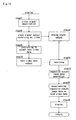
- Fig. 9 is a flowchart for use with the test apparatus 1 and the display device 3 according to this Embodiment.
- step 1 the test apparatus 1 is initialized. Then, in step 2, the display device 3 is inspected. Then, in step 3, the inspection result image data is displayed on the display unit 31 of the display device 3.
- Fig. 10 illustrates an initializing flowchart in step 1 of Fig. 9 .
- the processing at the left shows the processing for the test apparatus 1, while the processing at the right indicates the processing for the display device 3.
- step 10 the test apparatus 1 is initialized. More specifically, this step can be described as below.
- the control circuit 12 outputs a switching signal to the switch circuit 154 ( Fig. 3 ) of the test pattern generation circuit 15 to switch the test pattern generation circuit 15 so as to output the PN pattern. Additionally, the control circuit 12 initializes the jitter signal generation circuit 17.
- step 11 the test apparatus 1 instructs the display device 3 to start the test. More specifically, this step can be described as below.
- the control circuit 12 of the test apparatus 1 commands the control signal transmission circuit 13 to send a control signal for commanding the commencement of the test to the control signal reception circuit 32 of the display device 3.
- control signal transmission circuit 13 of the test apparatus 1 sends the control signal for commanding the commencement of the test to the control signal reception circuit 32 of the display device 3.
- step 12 the control signal reception circuit 32 of the display device 3 outputs the display switching signal to the display switching circuit 36 to turn on the display switching circuit 36.
- step 13 the control signal transmission circuit 33 of the display device 3 transmits a control signal for informing the completion of preparation for the test to the control signal reception circuit 14 of the test apparatus 1.
- step 14 the control signal reception circuit 14 of the test apparatus 1 receives the control signal for informing the completion of preparation for the test and then informs this to the control circuit 12.
- Fig. 11 illustrates an inspection flowchart in step 2 of Fig. 9 .
- the processing at the left shows the processing for the test apparatus 1, while the processing at the right indicates the processing for the display device 3.
- step 20 the phase modulation circuit 19 of the test apparatus 1 outputs the clock signal clk3 containing the jitter to the test pattern generation circuit 15 and the PLL circuit 39 of the display device 3.
- step 21 the test pattern generation circuit 15 of the test apparatus 1 outputs the PN pattern having a constant number of bits in sync with the clock signal containing the jitter supplied by the phase modulation circuit 19.
- the data transmission circuit 18 of the test apparatus 1 transmits the PN pattern to the data reception circuit 38 of the display device 3.
- step 22 the PLL circuit 39 of the display device 3 generates the timing signal in sync with the received clock signal clk3 containing the jitter. Subsequently, the PLL circuit 39 outputs the generated timing signal to the data reception circuit 38 and the malfunction information generation circuit 41.
- step 23 when the PLL circuit 39 is in the lock loss state, the malfunction information generation circuit 41 which inputted the timing signal generates the lock loss signal and then outputs it to the inspection result image generation circuit 37 as the inspection information.
- step 24 the data reception circuit 38 of the display device 3 captures the PN pattern transmitted by the data transmission circuit 18 of the test apparatus 1, in sync with the timing signal supplied by the PLL circuit 39.
- the data reception circuit 38 outputs the received PN pattern as received data to the display switching circuit 36 and the error information generation circuit 40.
- step 25 the error information generation circuit 40 determines the data error rate of the received data and then outputs the resulting signal to the inspection result image generation circuit 37 as the inspection information.
- the inspection result image generation circuit 37 of the display device 3 adds one line of the inspection information (the jitter frequency, the presence or absence of the loss of lock of the PLL circuit 39, and the data error rate) to generate the image data (the inspection result image data) indicating the inspection information, which is in turn outputted to the display switching circuit 36.
- This inspection information (the jitter frequency, the presence or absence of the loss of lock of the PLL circuit 39, and the data error rate) is stored in a storage circuit (not shown).
- step 27 the display switching circuit 36 superimposes the inspection result image data outputted by the inspection result image generation circuit 37 on the received data (the PN pattern) outputted by the data reception circuit 38 and then outputs the resulting signal to the display unit 31.
- step 28 the display unit 31 displays the received data (the PN pattern) on which the inspection result image data is superimposed.
- step 29 the process proceeds to step 3 of Fig. 9 , and if not, the process proceeds to step 30 (step 29).
- step 30 the control circuit 12 of the test apparatus 1 changes the jitter frequency of the jitter signal generation circuit 17. Then, at this jitter frequency, the process performs processing from step 20 to step 29.
- the number of bits per one loop in the inspection flow shown in Fig. 11 is the number of inspection bits.
- the error information generation circuit 40 of Fig. 7 and Fig. 8 divides the number of inconsistent bits in the PN pattern by the number of inspection bits to thereby determine the data error rate (the bit error rate).
- step 3 of Fig. 9 is described below in detail.
- Fig. 12 illustrates a display flow in step 3 of Fig. 9 .
- the processing at the left shows the processing for the test apparatus 1, while the processing at the right indicates the processing for the display device 3.
- step 31 the control circuit 12 of the test apparatus 1 commands the jitter signal generation circuit 17 to deactivate the generation of the jitter signal.
- the jitter signal generation circuit 17 deactivates the generation of the jitter signal clk2 by zeroing the jitter amplitude Aj and the jitter frequency fj of the jitter signal clk2.
- step 32 the phase modulation circuit 19 of the test apparatus 1 outputs the clock signal clk3 containing no jitter to the test pattern generation circuit 15 and the PLL circuit 39 of the display device 3.
- step 33 the control circuit 12 of the test apparatus 1 outputs a switching signal to the switch circuit 154 ( Fig.3 ) of the test pattern generation circuit 15, thereby switching the test pattern generation circuit 15 to output test video data.
- step 34 the test pattern generation circuit 15 outputs the test video data in sync with the clock signal containing no jitter outputted by the phase modulation circuit 19.
- the data transmission circuit 18 of the test apparatus 1 transmits the test video data to the data reception circuit 38 of the display device 3.
- step 35 the PLL circuit 39 of the display device 3 generates a timing signal in sync with the clock signal containing no jitter transmitted by the phase modulation circuit 19 of the test apparatus 1.
- the PLL circuit 39 outputs the generated timing signal to the data reception circuit 38.
- step 36 the data reception circuit 38 of the display device 3 captures the test video data transmitted by the data transmission circuit 18 of the test apparatus 1, in sync with the timing signal outputted by the PLL circuit 39.
- the data reception circuit 38 outputs the received test video data as received data to the display switching circuit 36.
- the inspection result image generation circuit 37 of the display device 3 acquires the inspection information (the jitter frequency, the presence or absence of the loss of lock of the PLL circuit 39, and the data error rate) from the storage circuit (not shown) to generate the image data (the inspection result image data) indicating the inspection information.
- the inspection information the jitter frequency, the presence or absence of the loss of lock of the PLL circuit 39, and the data error rate
- the inspection result image generation circuit 37 outputs the generated inspection result image data to the display switching circuit 36.
- step 38 the display switching circuit 36 of the display device 3 superimposes the inspection result image data outputted by the inspection result image generation circuit 37 on the received data (the test video data) outputted by the data reception circuit 38 and then outputs the resulting signal to the display unit 31.
- step 39 the display unit 31 of the display device 3 displays the test video data on which the inspection result image data is superimposed.
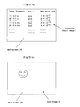
- Fig. 13 shows exemplary views of image data to be displayed on the display unit 31 of the display device 3 in step 39 of Fig. 12 .
- Fig. 13(a) is an example of the display provided when the display switching signal from the control signal reception circuit 32 of Fig. 1 is on
- Fig. 13(b) is an example of the display provided when the display switching signal from the control signal reception circuit 32 of Fig. 1 is off.
- step 12 of Fig. 10 the control signal reception circuit 32 enables the display switching signal to turn on the display switching circuit 36.
- this causes the test video data superimposing the inspection result image data to be displayed on the display unit 31 of the display device 3.
- test image A is displayed on a main screen 310 of the display unit 31, while an inspection result image B is displayed on a sub screen 311.
- control signal reception circuit 32 of the display device 3 has received the control signal transmitted by the control signal transmission circuit 13 of the test apparatus 1 and has thus been commanded to turn off the switching signal.
- the display switching circuit 36 is turned off, thereby causing the test video data to be outputted on the display unit 31.
- Fig. 14 is an exemplary view illustrating the inspection result image B to be displayed on the sub screen 311 of the display unit 31 of Fig. 13 .
- the jitter frequency, the presence or absence of the loss of lock of the PLL circuit 39, and the data error rate are displayed on the sub screen 311 of the display unit 31 as the inspection result image.
- "OK” indicates the locked state of the PLL circuit
- "NG” indicates the lock loss state of the PLL circuit.
- the display switching circuit 36 of the test apparatus 1 of Fig. 1 superimposes the inspection result image data on the test video data and then outputs the resulting signal to the display unit 31.
- the display switching circuit 36 can be employed as a simple switching circuit without this type of superimposition.
- step 12 of Fig. 10 the control signal reception circuit 32 has activated the display switching signal to thereby turn on the display switching circuit 36.
- the display switching circuit 36 outputs the inspection result image data outputted by the inspection result image generation circuit 37 onto the display unit 31 without the superimposition in step 38 of Fig. 12 .
- the control signal reception circuit 32 of the display device 3 has received the control signal transmitted by the control signal reception circuit 14 of the test apparatus 1 and has thus been instructed to turn off the display switching signal.
- the display switching circuit 36 is turned off causing the test video data to be outputted onto the display unit 31.
- Fig. 15 shows other exemplary views of image data to be displayed on the display unit 31 of the display device 3 in step 39 of Fig. 12 .
- Fig. 15(a) shows an exemplary representation provided when the display switching signal from the control signal reception circuit 32 of Fig. 1 is turned on
- Fig. 15(b) shows an exemplary representation provided when the display switching signal from the control signal reception circuit 32 of Fig. 1 is turned off.
- the inspection result image B is displayed on the main screen 310 of the display unit 31.
- the inspection result image B displayed here is an image as shown in Fig. 14 .
- the test image A is displayed on the main screen 310 of the display unit 31.
- the timing signal is supplied to the data reception circuit 38 of the display device 3 of Fig. 1 in sync with the clock signal containing the jitter (see steps 20 and 22 of Fig. 11 ).
- Other main factors that affect the data error rate include noise from other circuits, and thus the data error rate includes the influence caused by the noise.
- the clock signal containing the jitter is supplied to the PLL circuit 39 of the display device 3 of Fig. 1 (see steps 20 and 22 of Fig. 11 ).
- Other main factors that affect the PLL circuit 39 include noise from other circuits, and thus the loss of lock of the PLL circuit 39 includes the influence caused by the noise.
- test mode has been described. Now, with reference to Fig. 2 , the operation in the normal mode will be briefly described below.
- control signal transmission circuit 63 of the video data transmitter 6 transmits a control signal for informing of the transmission of the video data to the control signal reception circuit 32 of the display device 3 via the cable 5.
- the control signal reception circuit 32 receives the control signal.
- the component 8 for receiving the test related control signal e.g., a pin provided in the case of the reception circuit 30 comprising an integrated circuit
- the control signal transmission circuit 33 of the display device 3 transmits display control information, such as the resolution of the display device 3, to the control signal reception circuit 64 of the video data transmitter 6 via the cable 5.
- the clock signal generation circuit 61 of the video data transmitter 6 generates a clock signal to transmit it to the video generation circuit 60 and the PLL circuit 39 of the display device 3.
- the video generation circuit 60 outputs the video data in sync with the clock signal supplied by the clock signal generation circuit 61.
- the data transmission circuit 62 transmits the video data outputted by the video generation circuit 60 to the data reception circuit 38 of the display device 3 via the cable 5.
- the data reception circuit 38 of the display device 3 captures the video data in sync with the timing signal that is generated by the PLL circuit 39 in sync with the clock signal.
- the data reception circuit 38 outputs the captured video data to the display switching circuit 36.
- the display switching circuit 36 since the display switching circuit 36 is in an off state, the video data is outputted to the display unit 31 for display.
- the inspection circuit 35 is provided inside the display device 3 of Fig. 1 .
- the data reception related circuit 34 is inspected and the inspection information (the data error rate and the lock loss signal) is generated.
- the inspection result image generation circuit 37 generates the image data (the inspection result image data) indicating the inspection information, and the inspection result image data is displayed on the display unit 31 provided with the display device 3 ( Fig. 13 through Fig. 15 ).
- the inspection result image data is displayed on the display unit 31 incorporated into the display device 3, it is not required to provide an additional terminal outside the display device 3 to output the inspection result image data.
- control signal reception circuit 32 of the display device 3 receives the test related control signal from the test apparatus 1. Additionally, the control signal reception circuit 32 can receive and process an external signal other than the test related control signal via the component 8 for receiving the test related control signal.
- the display device 3 proceeds to the test mode.
- control signal reception circuit 32 of the display device 3 can receive and process the external signal other than the test related control signal. This makes it possible for the display device 3 to change to the normal mode by transmitting to the control signal reception circuit 32 an external control signal for instructing it to return to the normal mode. Additionally, the display device 3 can proceed to the test mode by only transmitting the control signal for instructing the commencement of the test to the control signal reception circuit 32 from the test apparatus 1 external thereto.
- control signal reception circuit 32 of the display device 3 can receive and process an external signal other than the test related control signal, control signal reception circuit 32 can receive and process the signal transmitted by the video data transmitter 6 external thereto.
- the present invention provides the control signal reception circuit 32 that can operate not only in the test mode but also in the normal mode.
- control signal reception circuit 32 uses the common component 8 in either the test mode or normal mode.
- control signal transmission circuit 33 of the display device 3 can transmit the test related control signal. Additionally, the control signal transmission circuit 33 can transmit a signal other than the test related control signal via the component 9 for transmitting the test related control signal to the outside.
- control signal transmission circuit 33 This makes it possible for the control signal transmission circuit 33 to transmit a signal to the external video data transmitter 6 via the component 9 for transmitting the test related control signal to the outside.
- control signal transmission circuit 33 This makes it possible for the control signal transmission circuit 33 to transmit signals as required to the external video data transmitter 6 after it proceeds to the normal mode.
- the present invention provides the control signal transmission circuit 33 that can operate not only in the test mode but also in the normal mode.
- control signal transmission circuit 33 uses the common component 9 in either the test mode or normal mode.
- the display switching circuit 36 of the display device 3 superimposes the inspection result image data generated by the inspection result image generation circuit 37 on the test signal (test video data) inputted by the data reception circuit 38 and then outputs the resulting signal to the display unit 31.
- the display switching circuit 36 outputs either one of the video data or the test video data superimposing the inspection result image data to the display unit 31. This makes it possible to share the component for outputting the video data to the display unit 31 and the component for outputting the test video data superimposing the inspection result image data to the display unit 31.
- the display switching circuit 36 receives the video data from the data reception circuit 38 to output it to the display unit 31 in the normal mode.
- the display switching circuit 36 receives the inspection result image data generated by the inspection result image generation circuit 37 and then outputs it to the display unit 31.
- the function for enabling superimposition can be eliminated when the display switching circuit 36 is used simply as the switching circuit, thereby making it possible to simplify the display switching circuit 36.
- the display switching circuit 36 employed simply as the switching circuit outputs either one of the video data or the inspection result image data generated by the inspection result image generation circuit 37 to the display unit 31. This makes it possible to share the component for outputting the video data to the display unit 31 and the component for outputting the inspection result image data generated by the inspection result image generation circuit 37 to the display unit 31.
- the display switching circuit 36 employed simply as the switching circuit receives the inspection result image data generated by the inspection result image generation circuit 37 in accordance with the control signal for instructing a display switchover received by the control signal reception circuit 32 to output the data to the display unit 31.
- the display switching circuit 36 receives the test video data as the test signal and then outputs the test video data to the display unit 31.
- the display switching circuit 36 employed simply as the switching circuit outputs either one of the inspection result image data or the test video data to the display unit 31 in accordance with the control signal. This makes it possible to share the component for outputting the inspection result image data to the display unit 31 and the component for outputting the test video data to the display unit 31.
- the data reception circuit 38 of the display device 3 receives the video data in the normal mode, while receiving the PN pattern as the test signal in the test mode.
- the error information generation circuit 40 of the display device 3 generates the data error rate of the PN pattern received by the data reception circuit 38.
- the data error rate is then displayed on the display unit 31 (see Fig. 14 ).
- the PLL circuit 39 receives the clock signal in the normal mode, while receiving the clock signal containing the jitter as the test signal, generating the timing signal in sync therewith.
- the malfunction information generation circuit 41 generates the lock loss signal when the PLL circuit 39 locking is lost.
- the presence or absence of the loss of lock is displayed on the display unit 31 (see Fig. 14 ).
- the data reception circuit 38 of the display device 3 receives the video data in sync with the timing signal based on the clock signal in the normal mode, while receiving the PN pattern as the test signal in sync with the timing signal based on the clock signal containing the jitter.
- the data error rate can be determined on the PN pattern received in sync with the timing signal in this manner, thereby providing the findings on the effects of the jitter.
- the inspection circuit 35 inspects the data reception related circuit 34 to generate the inspection information, and the image data (the inspection result image data) indicating the inspection information is displayed on the display unit 31.
- test apparatus 1 As described above, the following holds true for the test apparatus 1 according to this embodiment.
- control signal transmission circuit 13 of the test apparatus 1 receives the command from the control circuit 12 and then transmits the control signal for instructing the commencement of the test to the display device 3.
- the display device 3 for receiving the test signal can be made ready for the test in a simple manner by only transmitting the control signal to the display device 3.
- control circuit 12 of the test apparatus 1 instructs the jitter frequency as a test condition to the jitter signal generation circuit 17 of the test signal generation circuit 10.
- the test pattern generation circuit 15 of the test apparatus 1 generates the PN pattern as the test signal.
- the PN pattern is then transmitted to the display device 3.
- phase modulation circuit 19 of the test apparatus 1 superimposes the jitter signal clk2 on the clock signal clk1 to generate the clock signal clk3 containing the jitter, and then transmits the clock signal clk3 containing the jitter as the test signal to the PLL circuit 39 of the display device 3.
- the test pattern generation circuit 15 of the test apparatus 1 outputs the PN pattern to the data transmission circuit 18 in sync with the clock signal containing the jitter generated by the phase modulation circuit 19.
- the test apparatus 1 transmits the test signal (the PN pattern, the test video data, and the clock signal clk3 containing jitter) to the display device 3 via the cable 5.
- test can be carried out with the test apparatus 1 being connected not via the cable 5 but directly to the display device 3.
- test video data generation circuit 153 of Fig. 3 can be eliminated.
- the display switching circuit 36 of the display device 3 of Fig. 1 is employed simply as a switching circuit.
- a test apparatus receives inspection information from a display device to generate inspection result image data, which is in turn transmitted to the display device. This will be described below in detail.
- Fig. 16 is a block diagram illustrating an exemplary test apparatus 1 and an exemplary display device according to Embodiment 2, which is according to the present invention. Referring to Fig. 16 , the same components as those of Fig. 1 are indicated with the same reference numerals, and their descriptions will be omitted as appropriate.
- the test apparatus 8 is connected to the display device 7 via a cable 5.
- the test apparatus 8 comprises a test signal generation circuit 80, a test signal transmission circuit 11, a control circuit 12, a control signal transmission circuit 13, a control signal reception circuit 14, an inspection result image generation circuit 82, and an inspection information storage circuit 83.
- the test signal generation circuit 80 includes a test pattern generation circuit 15, a clock signal generation circuit 16, a jitter signal generation circuit 17, and a superimposition circuit 81.
- the test signal transmission circuit 11 includes a data transmission circuit 18 and a phase modulation circuit 19.
- the display device 7 comprises a reception circuit 70 and a display unit 31.
- the reception circuit 70 includes a data reception related circuit 34, an inspection circuit 35, a control signal reception circuit 32, and a control signal transmission circuit 33.
- the data reception related circuit 34 includes a data reception circuit 38 and a PLL (Phase Locked Loop) circuit 39.
- PLL Phase Locked Loop
- the inspection circuit 35 includes an error information generation circuit 40 and a malfunction information generation circuit 41.
- the reception circuit 70 may be configured as an integrated circuit (LSI).
- LSI integrated circuit
- this "component” means a signal input/output "pin" of the LSI.
- the “component” includes other known terminals.
- test apparatus 8 of Fig. 16 sends the test signal via the cable 5 to carry out the test on the display device 7.
- the state in which the display device 7 is ready for the test or carrying out the test is called the "test mode".
- the display device 7 receives the video data from the video data transmitter 6 of Fig. 2 to display it on the display unit 31.
- This normal state of operation is called "normal mode".
- the operation in the normal mode is the same as in Embodiment 1.
- the display device 7 of Fig. 16 is not provided with the display switching circuit 36 and the inspection result image generation circuit 37.
- the other components are provided for the display device 7 of Fig. 16 as well as for the display device 3 of Fig. 1 , and thus their descriptions are omitted.
- the information indicating the data error rate generated by the error information generation circuit 40 and the lock loss signal generated by the malfunction information generation circuit 41 are outputted to the control signal transmission circuit 33.
- the test apparatus 8 has the test pattern generation circuit 15, the clock signal generation circuit 16, the jitter signal generation circuit 17, the test signal transmission circuit 11, the control circuit 12, the control signal transmission circuit 13, and the control signal reception circuit 14, which are the same as the test pattern generation circuit 15, the clock signal generation circuit 16, the jitter signal generation circuit 17, the test signal transmission circuit 11, the control circuit 12, the control signal transmission circuit 13, and the control signal reception circuit 14 of the test apparatus 1 of Fig. 1 , respectively.
- the descriptions of these components are omitted.
- control signal reception circuit 14 receives the inspection information (the presence or absence of the loss of lock of the PLL circuit 39, and the information indicating the data error rate) transmitted by the control signal transmission circuit 33 of the display device 7, and then outputs the information to the inspection information storage circuit 83.
- the inspection information storage circuit 83 stores the inspection information.
- the inspection result image generation circuit 82 acquires the inspection information from the inspection information storage circuit 83 to generate the image data indicating the inspection information.
- the image data indicating inspection information may hereinafter be referred to as "inspection result image data”.
- an image indicating the inspection information may hereinafter be referred to as "inspection result image”.
- the inspection result image generation circuit 82 outputs the generated inspection result image data to the superimposition circuit 81.
- the superimposition circuit 81 superimposes the inspection result image data on the test signal (the PN pattern or the test video data) generated by the test pattern generation circuit 15, and then outputs the resulting signal to the data transmission circuit 18.
- the data reception circuit 38 of the display device 7 receives the test signal superimposing the inspection result image data from the data transmission circuit 18 of the test apparatus 8, and then outputs the resulting signal to the display unit 31.
- the display unit 31 displays the test signal superimposing the inspection result image data.
- step 1 the test apparatus 8 is initialized. Then, in step 2, the display device 7 is inspected. Then, in step 3, the inspection result image data is displayed on the display unit 31 of the display device 7.
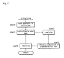
- Fig. 17 illustrates the initializing flow in step 1 of Fig. 9 .
- the processing at the left shows the processing for the test apparatus 8, while the processing at the right indicates the processing for the display device 7.
- step 10 the test apparatus 8 is initialized. More specifically, this step can be described as below.
- the control circuit 12 of the test apparatus 8 outputs the switching signal to the switch circuit 154 ( Fig. 3 ) of the test pattern generation circuit 15 to switch the test pattern generation circuit 15 so as to output the PN pattern. Additionally, the control circuit 12 initializes the jitter signal generation circuit 17.
- step 11 the test apparatus 8 instructs the display device 7 to start test. More specifically, this step can be described as below.
- the control circuit 12 of the test apparatus 8 commands the control signal transmission circuit 13 to send the control signal for the commencement of the test to the control signal reception circuit 32 of the display device 7.
- control signal transmission circuit 13 of the test apparatus 8 sends the control signal for commanding the commencement of the test to the control signal reception circuit 32 of the display device 7.
- step 12 the control signal reception circuit 32 of the display device 7 receives the control signal for instructing the commencement of the test.
- the inspection information the information indicating the presence or absence of the loss of lock of the PLL circuit 39 and the information indicating the data error rate
- step 13 the control signal transmission circuit 33 of the display device 7 transmits the control signal for informing the completion of preparation for the test to the control signal reception circuit 14 of the test apparatus 8.
- step 14 the control signal reception circuit 14 of the test apparatus 8 receives the control signal for informing the completion of preparation for the test and then informs the control circuit 12 of it.
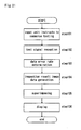
- Fig. 18 illustrates the inspection flow in step 2 of Fig. 9 .
- the processing at the left shows the processing for the test apparatus 8, while the processing at the right indicates the processing for the display device 7.
- step 20 the phase modulation circuit 19 of the test apparatus 8 outputs the clock signal clk3 containing the jitter to the test pattern generation circuit 15 and the PLL circuit 39 of the display device 7.
- step 21 the test pattern generation circuit 15 of the test apparatus 8 outputs the PN pattern having the constant number of bits in sync with the clock signal containing the jitter supplied by the phase modulation circuit 19.
- step 22 the superimposition circuit 81 of the test apparatus 8 superimposes the inspection result image data generated by the inspection result image generation circuit 82 of the test apparatus 8 on the PN pattern, and then outputs the resulting signal to the data transmission circuit 18, with the inspection result image being blank at first.
- the data transmission circuit 18 of the test apparatus 8 transmits the PN pattern superimposing the inspection result image data to the data reception circuit 38 of the display device 7.
- step 23 the PLL circuit 39 of the display device 7 generates the timing signal in sync with the received clock signal clk3 containing the jitter. Subsequently, the PLL circuit 39 outputs the generated timing signal to the data reception circuit 38 and the malfunction information generation circuit 41.
- step 24 when the PLL circuit 39 is in the lock loss state, the malfunction information generation circuit 41 having inputted the timing signal generates the lock loss signal and then outputs it to the control signal transmission circuit 33 as the inspection information.
- control signal transmission circuit 33 In response to this lock loss signal, the control signal transmission circuit 33 generates the information indicating the presence or absence of the loss of lock of the PLL circuit 39.
- step 25 the data reception circuit 38 of the display device 7 captures the PN pattern superimposing the inspection result image data, in sync with the timing signal supplied by the PLL circuit 39.
- the PN pattern superimposing the inspection result image data is transmitted to the data reception circuit 38 by the data transmission circuit 18 of the test apparatus 8.
- the data reception circuit 38 outputs the received PN pattern as the received data to the display unit 31 and the error information generation circuit 40.
- step 25 the error information generation circuit 40 determines the data error rate of the received data and then outputs the resulting signal to the control signal transmission circuit 33 as the inspection information.
- step 27 the control signal transmission circuit 33 of the display device 7 transmits the inspection information (the information indicating the presence or absence of the loss of lock of the PLL circuit 39 and the information indicating the data error rate) to the control signal reception circuit 14 of the test apparatus 8.
- the inspection information the information indicating the presence or absence of the loss of lock of the PLL circuit 39 and the information indicating the data error rate
- step 28 the control signal reception circuit 14 outputs the received inspection information to the inspection information storage circuit 83.
- the inspection result image generation circuit 82 acquires the inspection information from the inspection information storage circuit 83 to generate the inspection result image data, and then outputs the data to the superimposition circuit 81.
- step 29 the process proceeds to step 3 of Fig. 9 , and if not, the process proceeds to step 30 (step 29).
- step 30 the control circuit 12 of the test apparatus 8 changes the jitter frequency of the jitter signal generation circuit 17. Then, at that jitter frequency, processing 20 through 29 are performed.
- the number of bits per one loop in the inspection flow shown in Fig. 18 is the number of inspection bits.
- the error information generation circuit 40 of Fig. 7 and Fig. 8 divides the number of inconsistent bits in the PN pattern by the number of inspection bits to thereby determine the data error rate.
- step 3 of Fig. 9 is described below in detail.
- Fig. 19 illustrates the display flowchart in step 3 of Fig. 9 .
- the processing at the left shows the processing for the test apparatus 8, while the processing at the right indicates the processing for the display device 7.
- step 31 the control circuit 12 of the test apparatus 8 commands the jitter signal generation circuit 17 to deactivate the generation of the jitter signal.
- the jitter signal generation circuit 17 deactivates the generation of the jitter signal clk2 by zeroing the jitter amplitude Aj and the jitter frequency fj of the jitter signal clk2.
- step 32 the phase modulation circuit 19 of the test apparatus 8 outputs the clock signal clk3 containing no jitter to the test pattern generation circuit 15 and the PLL circuit 39 of the display device 7.
- step 33 the control circuit 12 of the test apparatus 8 outputs the switching signal to the switch circuit 154 ( Fig.3 ) of the test pattern generation circuit 15, thereby switching the test pattern generation circuit 15 so as to output the test video data.
- step 34 the test pattern generation circuit 15 outputs the test video data in sync with the clock signal containing no jitter outputted by the phase modulation circuit 19.
- step 35 the inspection information storage circuit 83 of the test apparatus 8 outputs the stored inspection information to the inspection result image generation circuit 82, while the inspection result image generation circuit 82 generates the inspection result image data.
- step 36 the superimposition circuit 81 of the test apparatus 8 superimposes the inspection result image data generated by the inspection result image generation circuit 82 on the test video data outputted by the test pattern generation circuit 15, and then outputs the resulting signal to the data transmission circuit 18.
- step 37 the PLL circuit 39 of the display device 7 generates the timing signal in sync with the clock signal containing no jitter transmitted by the phase modulation circuit 19 of the test apparatus 8.
- the PLL circuit 39 outputs the generated timing signal to the data reception circuit 38.
- step 38 the data reception circuit 38 of the display device 7 captures the test video data superimposing the inspection result image data, in sync with the timing signal outputted by the PLL circuit 39.
- the test video data superimposing the inspection result image data is transmitted to the data reception circuit 38 by the data transmission circuit 18 of the test apparatus 8.
- the data reception circuit 38 outputs the test video data superimposing the inspection result image data to the display unit 31 as the received data.
- step 39 the display unit 31 of the display device 7 displays the test video data on which the inspection result image data is superimposed.
- This display example is the same as that in Fig. 13(a) and Fig. 14 .
- the inspection circuit 35 is provided inside the display device 7 of Fig. 16 .
- the data reception related circuit 34 is inspected and the inspection information (the data error rate and the lock loss signal) is generated.
- control signal transmission circuit 33 transmits the inspection information (the data error rate and the presence or absence of loss of lock) to the test apparatus 8, and the inspection result image generation circuit 82 of the test apparatus 8 generates the inspection result image data.
- the test apparatus 8 then transmits the test video data superimposing the inspection result image data to the display device 7, allowing the display unit 31 of the display device 7 to display it.
- the inspection result image data is generated in the test apparatus 8, it is not necessary to provide a circuit for generating the inspection result image data inside the display device 7 to be tested. This alleviates the level of complication of the display device 7 when compared with Embodiment 1.
- test video data superimposing the inspection result image data to the display device 7 from the test apparatus 8 external thereto, it is possible to check the inspection result of the data reception related circuit 34 at the display unit 31 of the display device 7 and visually inspect the test video data as well.
- the inspection result image data is generated externally and then the data reception circuit 38 that receives the video data in the normal mode receives the test video data superimposing the inspection result image data to output the data to the display unit 31.
- control signal reception circuit 32 of the display device 7 receives the test related control signal. Additionally, the control signal reception circuit 32 can receive and process the external signal other than the test related control signal via the component 8 for receiving the test related control signal.
- the display device 7 can proceed to the test mode by only transmitting the control signal for instructing the commencement of the test to the control signal reception circuit 32 from the test apparatus 8 external thereto.
- the modes can be switched only with the control signal outside the display device 7.
- control signal reception circuit 32 can receive and process the external signal other than the test related control signal, the control signal reception circuit 32 can receive and process the control signal transmitted by the video data transmitter 6 external thereto.
- the present invention provides the control signal reception circuit 32 that can operate not only in the test mode but also in the normal mode.
- control signal reception circuit 32 uses the common component 8 in either the test mode or the normal mode.
- control signal transmission circuit 33 can transmit the control signal other than the test related control signal via the component 9 for transmitting the test related control signal to the outside. This makes it possible to transmit signals to the external video data transmitter 6.
- control signal transmission circuit 33 This in turn makes it possible for the control signal transmission circuit 33 to transmit signals as required to the external video data transmitter 6 after it proceeds to the normal mode.
- the present invention provides the control signal transmission circuit 33 that can operate not only in the test mode but also in the normal mode.
- control signal transmission circuit 33 uses the common component 9 in either the test mode or the normal mode.
- control signal transmission circuit 33 and the control signal reception circuit 32 are provided, thereby eliminating the need for providing the display device 7, on its exterior, with an additional dedicated terminal for the output of the inspection information or an additional dedicated terminal for the input of the inspection result image data.
- the data reception circuit 38 of the display device 7 receives the video data in the normal mode, while receiving the PN pattern as the test signal in the test mode.
- the error information generation circuit 40 of the display device 7 generates the data error rate of the PN pattern received by the data reception circuit 38.
- the control signal transmission circuit 33 inside the display device 7 then transmits the information indicating the data error rate generated by the error information generation circuit 40 to the outside as the inspection information.
- the PLL circuit 39 of the display device 7 receives the clock signal in the normal mode, while receiving the clock signal containing the jitter as the test signal, generating the timing signal in sync therewith.
- the malfunction information generation circuit 41 generates the lock loss signal when the PLL circuit 39 locking is lost.
- control signal transmission circuit 33 transmits the information indicating the presence or absence of the loss of lock of the PLL circuit 39 as the inspection information to the outside.
- the data reception circuit 38 of the display device 7 receives the video data in sync with the timing signal based on the clock signal in the normal mode, while receiving the PN pattern in the test mode in sync with the timing signal based on the clock signal containing the jitter.
- the error information generation circuit 40 of the display device 7 determines the data error rate of the PN pattern received in sync with the timing signal in this manner, thereby making it possible to provide the findings on the effects of the jitter.
- the inspection circuit 35 inspects the data reception related circuit 34 to generate the inspection information, and the image data (the inspection result image data) indicating the inspection information is displayed on the display unit 31.
- test apparatus 8 As described above, the following holds true for the test apparatus 8 according to this embodiment.
- control signal transmission circuit 13 of the test apparatus 8 receives the command from the control circuit 12 and then transmits the control signal for instructing the commencement of the test to the display device 7.
- the display device 7 for receiving the test signal can be made ready for the test in a simple manner by only transmitting the control signal to the display device 7.
- the inspection result image data is generated in the test apparatus 8, it is not necessary to provide a circuit for generating the inspection result image data inside the display device 7 to be tested. This alleviates the level of complication of the display device 7.
- the superimposition circuit 81 of the test apparatus 8 superimposes the inspection result image data on the test video data and then outputs the resulting data to the data transmission circuit 18.
- the data transmission circuit 18 of the test apparatus 8 transmits the test video data superimposing the inspection result image data to the display device 7.
- test apparatus 8 is provided with the control circuit 12. As in Embodiment 1, this alleviates the time and manpower for setting the test condition that has been conventionally set manually.
- the test pattern generation circuit 15 of the test apparatus 8 generates the PN pattern as the test signal.
- the PN pattern is then transmitted to the display device 7.
- phase modulation circuit 19 of the test apparatus 8 superimposes the jitter signal clk2 on the clock signal clk1 to generate the clock signal clk3 containing the jitter, and then transmits the clock signal clk3 containing the jitter as the test signal to the PLL circuit 39 of the display device 7.
- the test pattern generation circuit 15 of the test apparatus 8 outputs the PN pattern to the data transmission circuit 18 in sync with the clock signal containing the jitter generated by the phase modulation circuit 19.
- the test apparatus 8 transmits the test signal (the PN pattern, the test video data, and the clock signal clk3 containing jitter) to the display device 7 via the cable 5.
- test can also be carried out with the test apparatus 8 being connected not via the cable 5 but directly to the display device 7.
- test video data generation circuit 153 of Fig. 3 can be eliminated.
- the superimposition circuit 81 of Fig. 16 is replaced with a switching circuit.
- the control circuit 12 commands the switching circuit to display the inspection result image data on the display device 7
- the data transmission circuit 18 outputs the inspection result image data
- the PN pattern is outputted to the data transmission circuit 18 when the inspection is carried out for the data reception related circuit 34 of the display device 7.
- the technique of the literature aiming not to damage the integrated circuit is significantly different from the present invention in that the object of the present invention is to inspect the display device without having to disassemble the display device and without changing the noise environment thereof.
- the technique of the literature is to connect a known IC tester to the test input pins and output pins of the integrated circuit to measure the jitter of the PLL circuit. Accordingly, in consideration of the integrated circuit being built in the display device, the display device must be disassembled to inspect the integrated circuit, thereby making it impossible to address the object of the present invention.
- the technique of the literature is limited to jitter information, and never refers to the data error rate and the lock loss signal of the PLL circuit.
- the literature does not disclose any specific means for outputting signals to outside the integrated circuit, such as the display switching circuit 36 according to this embodiment.
- Fig. 20 is a block diagram illustrating a video data transmitter and a display device according to Embodiment 3 useful for understanding the present invention.
- Fig. 20 the same components as those of Fig. 1 are indicated with the same reference numerals.
- the video data transmitter 100 is connected to the display device 200 via a cable 5.
- the display device 200 comprises a reception circuit 201, an input unit 206, and a display unit 31.
- the reception circuit 201 includes a data reception related circuit 202, an inspection circuit 204, a display switching circuit 36, and an inspection result image generation circuit 37.
- the data reception related circuit 202 includes a data reception circuit 38.
- the inspection circuit 204 includes an error information generation circuit 40.
- the video data transmitter 100 transmits video data such as movies to the display device 200 via the cable 5 when the display device 200 is in the normal mode.
- the video data transmitter 100 is the same as the video data transmitter 6 of Fig. 2 and, for example, incorporated into a personal computer, a set top box (STB), a DVD (Digital Video Disc) player or the like.
- STB set top box
- DVD Digital Video Disc
- the video data transmitter 100 transmits a test signal to the display device 200 via the cable 5 when the display device 200 is in the test mode.
- the test signal includes test video data or a PN pattern.
- the test video data includes test image data or a color pattern or both the test image data and the color pattern.
- the test image data includes test moving image data or test static image data.
- the test image data is an image produced by photographing an object while the color pattern is a patterned image.
- test mode The state in which the display device 200 is ready for a test or carrying out the test is called hereafter the "test mode".
- the video data transmitter 100 is able to read video data stored on a storage medium.
- the video data transmitter 100 is allowed to read out the test signal by setting thereto a storage medium having the test signal recorded thereon, and then transmits the test signal to the display device 200.
- the video data transmitter 100 is the DVD player.
- the video data transmitter 100 is allowed to read out the test signal by setting thereto a DVD having the test signal recorded thereon, and then transmits the test signal to the display device 200.
- the video data transmitter 100 is provided with a storage device having the test signal recorded therein.
- the video data transmitter 100 is allowed to read out the test signal from the storage device and then transmits it to the display device 200.
- the video data transmitter 100 is the set top box equipped with a ROM (Read Only Memory) having the test signal recorded thereon.
- the video data transmitter 100 is allowed to read out the test signal from the ROM and then transmits the signal to the display device 200.
- the input unit 206 of the display device 200 instructs the display switching circuit 36 to move into the test mode or move out of the test mode.
- the display device 200 is placed in the test mode.
- the display device 200 is switched from the test mode into the normal mode.
- the input unit 206 includes an interface with the outside such as a button, a switch, a sensor for receiving a signal from an infrared remote controller, or a terminal other than a terminal for inputting the video data. Via this interface, the input unit 206 receives an instruction (to move into or out of the test mode) from the outside.
- an interface e.g., a button, a switch, a sensor for receiving a signal from an infrared remote controller, or a terminal other than a terminal for inputting the video data
- an interface e.g., a button, a switch, a sensor for receiving a signal from an infrared remote controller, or a terminal other than a terminal for inputting the video data
- the reception circuit 201 receives the video data transmitted by the video data transmitter 100 and then outputs the data to the display unit 31.
- the reception circuit 201 receives the test signal transmitted by the video data transmitter 100.
- reception circuit 201 configured as mentioned above with reference to Fig. 20 , is described in detail as below.
- the data reception related circuit 202 of the display device 200 is described below.
- the data reception related circuit 202 receives the test signal transmitted by the video data transmitter 100. -
- the data reception related circuit 202 receives the video data transmitted by the video data transmitter 100.
- the inspection circuit 204 of the display device 200 inspects the data reception related circuit 202 to generate inspection information and then outputs the information to the inspection result image generation circuit 37.
- the inspection result image generation circuit 37 of the display device 200 receives the inspection information generated by the inspection circuit 204.
- the inspection result image generation circuit 37 generates image data indicating the inspection information received.
- the image data indicating the inspection information may hereinafter be referred to as "inspection result image data”.
- an image indicating the inspection information may hereinafter be referred to as "inspection result image”.
- the display switching circuit 36 of the display device 200 In the normal mode, the display switching circuit 36 outputs the video data received by the data reception related circuit 202 to the display unit 31.
- the display switching circuit 36 superimposes the inspection result image data generated by the inspection result image generation circuit 37 on the test signal received by the data reception related circuit 202 and then outputs the resulting signal to the display unit 31.
- the display switching circuit 36 provides different operations between the normal mode (without the superimposition) and test mode (with the superimposition). The switching between the operations is performed in accordance with the instructions from the input unit 206.
- the display switching circuit 36 superimposes the inspection result image data generated by the inspection result image generation circuit 37 on the test signal received by the data reception related circuit 202 and then outputs the resulting signal to the display unit 31.
- the display switching circuit 36 outputs the video data received by the data reception related circuit 202 to the display unit 31.
- the data reception related circuit 202 receives the test signal transmitted by the video data transmitter 100.
- the data reception circuit 38 outputs the received test signal to the display switching circuit 36 and the error information generation circuit 40 of the inspection circuit 204.
- the data reception circuit 38 receives the video data transmitted by the video data transmitter 100 and then outputs the data to the display switching circuit 36.
- the inspection circuit 204 of Fig. 20 is described below in detail.
- the error information generation circuit 40 of the investigation circuit 204 generates data error information on the test signal received by the data reception circuit 38 and then outputs the data error information as the inspection information to the inspection result image generation circuit 37.
- the error information generation circuit 40 generates a "data error rate (bit error rate)" as the data error information.
- the reception circuit 201 of Fig. 20 described above can be configured as an integrated circuit (LSI).
- LSI integrated circuit
- this "component” means a signal input/output "pin" of the LSI.
- the “component” includes other known terminals.
- the display unit 31 of the display device 200 of Fig. 20 is described below.
- the display unit 31 displays the video data outputted by the display switching circuit 36.
- the display unit 31 displays image data generated by superimposing the inspection result image data on the test signal.
- the image data is outputted to the display unit 31 by the display switching circuit 36 in the test mode.
- Fig. 21 is a flowchart for use with the display device 200 in the test mode according to this embodiment.
- step 101 the input unit 206 instructs the display switching circuit 36 to commence testing.
- the input unit 206 instructs the display switching circuit 36 to move into the test mode.
- step 102 the data reception circuit 38 receives the test signal (the test video data and the PN pattern) from the video data transmitter 100.
- the data reception circuit 38 outputs the received test signal as received data to the display switching circuit 36 and the error information generation circuit 40.
- step 103 the error information generation circuit 40 determines the data error rate of the received data and then outputs the resulting signal as the inspection information to the inspection result image generation circuit 37.
- step 104 the inspection result image generation circuit 37 generates the image data (the inspection result image data) indicating the inspection information (the data error rate) and then outputs the data to the display switching circuit 36.
- step 105 the display switching circuit 36 superimposes the inspection result image data outputted by the inspection result image generation circuit 37 on the received data outputted by the data reception circuit 38 and then outputs the resulting data to the display unit 31.
- step 106 the display unit 31 displays the received data superimposing the inspection result image data.
- Fig. 22(a) is an exemplary view illustrating the test signal received in the test mode by the data reception circuit 38.
- Fig. 22(b) is an exemplary view illustrating the inspection result image data generated in the test mode by the inspection result image generation circuit 37.
- Fig. 22(c) is an exemplary view illustrating the image data to be displayed in the test mode on the display unit 31.
- the data reception circuit 38 has received the test signal "a" of Fig. 22 from the video data transmitter 100 in the test mode.
- the test signal "a” is comprised of the test moving image data "b", the color pattern "c", and the PN pattern (random image) "d".
- the test moving image data "b” and the color pattern "c" constitute the test video data.
- test signal "a" received by the data reception circuit 38 is outputted to the display switching circuit 36 and the error information generation circuit 40.
- test signal "a” is stored on the storage medium to be set in the video data transmitter 100 or in the storage device provided in the video data transmitter 100.
- the inspection result image generation circuit 37 generates the image data "e” indicating the data error rate of the PN pattern "d".
- the error information generation circuit 40 generates the data error rate of the PN pattern "d”.
- the image data "e” indicating the data error rate generated by the inspection result image generation circuit 37 is outputted to the display switching circuit 36.
- the display switching circuit 36 superimposes the inspection result image data "e” on the PN pattern "d" of the test signal "a” inputted from the data reception circuit 38.
- the display switching circuit 36 outputs the image data superimposing the inspection result image data "e” on the PN pattern "d” of the test signal "a” to the display unit 31.
- the display unit 31 then displays, on a screen 210 of the display unit 31, the image data generated by superimposing the inspection result image data "e” on the PN pattern "d" of the test signal "a”, or the image data formed of the test moving image data "b", the color pattern "c", and the inspection result image data "e”.
- the display switching circuit 36 can also output any one of the test signal "a” and the inspection result image data "e” to the display unit 31 in accordance with the instructions from the input unit 206.
- the display switching circuit 36 can also output any one piece of data selected from the group of the test moving image data "b", the color pattern "c", and the inspection result image data "e” to the display unit 31.
- the display switching circuit 36 can also output any two pieces of data selected from the group of the test moving image data "b", the color pattern "c", and the inspection result image data "e” to the display unit 31.
- the test signal "a” includes the test moving image data "b".
- the test signal "a” may be formed of the color pattern "c” and the PN pattern "d”.
- the test signal "a” includes the color pattern "c".
- the test signal "a” may be formed of the test moving image data "b" and the PN pattern "d".
- test moving image data "b" is employed as the test signal "a".
- test static image data may also be employed.
- test mode The operations of the test mode have been described. Now, with reference to Fig. 20 , the operations in the normal mode will be briefly described below.
- the video data transmitter 100 transmits the video data such as the movies to the display device 200 via the cable 5.
- the data reception circuit 38 of the display device 200 receives the video data from the video data transmitter 100 and then provides the video data to the display switching circuit 36.
- the display switching circuit 36 supplies the video data inputted from the data reception circuit 38 to the display unit 31.
- the display unit 31 displays the video data inputted from the display switching circuit 36.
- the inspection circuit 204 is provided inside the display device 200 of Fig. 20 .
- the data reception related circuit 202 is inspected and the inspection information (the data error rate) is generated.
- the inspection result image generation circuit 37 generates the image data (the inspection result image data) indicating the inspection information and the inspection result image data is displayed on the display unit 31 provided with the display device 200 ( Fig. 22(c) ).
- the inspection result image data is displayed in the display unit 31 provided with the display device 200, it is not necessary to provide a terminal for outputting the inspection result image data outside the display device 200.
- the display switching circuit 36 of the display device 200 superimposes the inspection result image data generated by the inspection result image generation circuit 37 on the test signal inputted from the data reception circuit 3 8 and then outputs the resulting signal to the display unit 31.
- the display switching circuit 36 outputs any one of the video data or the test signal superimposing the inspection result image data to the display unit 31. This makes it possible to share a component for outputting the video data to the display unit 31 and a component for outputting the test signal superimposing the inspection result image data to the display unit 31.
- the inspection circuit 204 inspects the data reception related circuit 202 to generate the inspection information and then the image data (the inspection result image data) indicating the inspection information is displayed on the display unit 31.
- test signal is also transmitted to the data reception related circuit 202 via the cable 5.
- the display device 200 is provided with the input unit 206 for instructing a switchover between the modes.
- the input unit 206 provided in the display device 200 can instruct the display device 200 to move into the test mode.
- the display device 200 can be tested in a simpler manner.
- the input unit 206 can instruct a switchover between the modes using the interface with the outside that is used in the normal mode.
Landscapes
- Engineering & Computer Science (AREA)
- Multimedia (AREA)
- Signal Processing (AREA)
- Health & Medical Sciences (AREA)
- Biomedical Technology (AREA)
- General Health & Medical Sciences (AREA)
- Testing, Inspecting, Measuring Of Stereoscopic Televisions And Televisions (AREA)
Applications Claiming Priority (3)
| Application Number | Priority Date | Filing Date | Title |
|---|---|---|---|
| JP2001344282 | 2001-11-09 | ||
| JP2001344282 | 2001-11-09 | ||
| PCT/JP2002/011476 WO2003041419A1 (en) | 2001-11-09 | 2002-11-01 | Display device, receiver, and test apparatus |
Publications (2)
| Publication Number | Publication Date |
|---|---|
| EP1442615A1 EP1442615A1 (en) | 2004-08-04 |
| EP1442615B1 true EP1442615B1 (en) | 2013-10-23 |
Family
ID=19157831
Family Applications (1)
| Application Number | Title | Priority Date | Filing Date |
|---|---|---|---|
| EP02775483.7A Expired - Lifetime EP1442615B1 (en) | 2001-11-09 | 2002-11-01 | Display device, receiver, and test apparatus |
Country Status (6)
| Country | Link |
|---|---|
| US (1) | US7103800B2 (https=) |
| EP (1) | EP1442615B1 (https=) |
| JP (1) | JP4295110B2 (https=) |
| KR (1) | KR20040053292A (https=) |
| CN (1) | CN1305320C (https=) |
| WO (1) | WO2003041419A1 (https=) |
Families Citing this family (29)
| Publication number | Priority date | Publication date | Assignee | Title |
|---|---|---|---|---|
| JP4323873B2 (ja) * | 2003-06-13 | 2009-09-02 | 富士通株式会社 | 入出力インタフェース回路 |
| JP4617302B2 (ja) * | 2004-03-22 | 2011-01-26 | 株式会社デジタル | 表示器、コンピュータを表示器として機能させるためのプログラムプロダクト、およびそのプログラムプロダクトを格納した記録媒体 |
| FR2875309B1 (fr) * | 2004-09-15 | 2006-12-22 | Alstom Transport Sa | Dispositif et procede de controle d'une console |
| DE102005024649B4 (de) * | 2005-05-25 | 2007-04-12 | Infineon Technologies Ag | Vorrichtung und Verfahren zum Messen von Jitter |
| KR100711739B1 (ko) * | 2005-07-21 | 2007-04-25 | 삼성전자주식회사 | 테스트 시스템 및 그것의 테스트 방법 |
| US7546507B1 (en) * | 2005-12-02 | 2009-06-09 | Altera Corporation | Method and apparatus for debugging semiconductor devices |
| CN100584046C (zh) * | 2005-12-27 | 2010-01-20 | 鸿富锦精密工业(深圳)有限公司 | 多媒体装置测试系统及其方法 |
| JP4923786B2 (ja) * | 2006-06-30 | 2012-04-25 | カシオ計算機株式会社 | ディスプレイ検査装置 |
| EP3200189B1 (en) * | 2007-04-12 | 2021-06-02 | Rambus Inc. | Memory system with point-to-point request interconnect |
| US20080275662A1 (en) * | 2007-05-01 | 2008-11-06 | Vladimir Dmitriev-Zdorov | Generating transmission-code compliant test sequences |
| CN101039443B (zh) * | 2007-05-15 | 2010-08-18 | 中兴通讯股份有限公司 | 一种数字电视接收终端电视功能故障的定位和显示方法 |
| JP5161484B2 (ja) * | 2007-05-17 | 2013-03-13 | オンセミコンダクター・トレーディング・リミテッド | 映像信号処理集積回路 |
| TW200924385A (en) | 2007-11-28 | 2009-06-01 | Realtek Semiconductor Corp | Jitter generator for generating jittered clock signal |
| CN102006160B (zh) * | 2007-12-24 | 2013-09-11 | 瑞昱半导体股份有限公司 | 用来产生抖动时钟信号的抖动产生器 |
| TWI406216B (zh) * | 2008-09-02 | 2013-08-21 | Himax Tech Ltd | 電壓寫入裝置及電壓寫入方法 |
| KR101651285B1 (ko) * | 2009-07-28 | 2016-08-26 | 삼성전자 주식회사 | 전자기기, 원격제어장치 및 오류검출방법 |
| KR101918627B1 (ko) | 2012-04-04 | 2018-11-15 | 삼성전자 주식회사 | 데이터 수신장치 및 그 테스트 방법 |
| US9436543B2 (en) * | 2012-09-13 | 2016-09-06 | Freescale Semiconductor, Inc. | Electronic device and method for protecting an electronic device against unauthorized use |
| CN103905513A (zh) * | 2012-12-28 | 2014-07-02 | 鸿富锦精密工业(深圳)有限公司 | 电子装置远程控制系统及方法 |
| TWI569238B (zh) * | 2014-10-13 | 2017-02-01 | 群創光電股份有限公司 | 顯示面板及顯示面板自動化檢測方法 |
| KR102317897B1 (ko) | 2015-06-04 | 2021-10-28 | 삼성디스플레이 주식회사 | 테스트 보드 및 그의 구동방법 |
| JP6726999B2 (ja) * | 2016-03-30 | 2020-07-22 | Dxアンテナ株式会社 | 検査システム |
| CN109522165B (zh) * | 2018-09-19 | 2020-05-15 | 昆山国显光电有限公司 | 显示模组测试平台 |
| JP7102450B2 (ja) * | 2020-01-31 | 2022-07-19 | アンリツ株式会社 | 誤り率測定システム及び誤り率測定方法 |
| CN115118958A (zh) * | 2022-06-14 | 2022-09-27 | 国营芜湖机械厂 | 一种机载任务处理机的视频信号检测装置及其检测方法 |
| CN114910733B (zh) * | 2022-07-15 | 2022-09-30 | 深圳益实科技有限公司 | 一种基于人工智能的显示器故障智能诊断分析系统 |
| CN115118961B (zh) * | 2022-08-26 | 2022-10-28 | 北京数字光芯集成电路设计有限公司 | 视频数据测试系统、方法及其应用 |
| KR20240114697A (ko) | 2023-01-17 | 2024-07-24 | 연세대학교 산학협력단 | 중합 고분자 전해질 기반 고체 후막 전극 및 그 제조방법 |
| KR20240125824A (ko) * | 2023-02-10 | 2024-08-20 | 삼성디스플레이 주식회사 | 표시 장치 |
Citations (1)
| Publication number | Priority date | Publication date | Assignee | Title |
|---|---|---|---|---|
| US6037978A (en) * | 1996-03-28 | 2000-03-14 | Samsung Electronics Co., Ltd. | Sync signal self-test device and method |
Family Cites Families (12)
| Publication number | Priority date | Publication date | Assignee | Title |
|---|---|---|---|---|
| GB9123105D0 (en) * | 1991-10-31 | 1991-12-18 | Crosfield Electronics Ltd | Calibration apparatus |
| US5572444A (en) * | 1992-08-19 | 1996-11-05 | Mtl Systems, Inc. | Method and apparatus for automatic performance evaluation of electronic display devices |
| JPH07170179A (ja) | 1993-12-16 | 1995-07-04 | Matsushita Electric Ind Co Ltd | Pllロック検出装置 |
| US5565897A (en) * | 1994-01-14 | 1996-10-15 | Elonex Technologies, Inc. | Interactive system for calibration of display monitors |
| US5969756A (en) * | 1994-06-13 | 1999-10-19 | Image Processing Systems Inc. | Test and alignment system for electronic display devices and test fixture for same |
| US5537145A (en) * | 1994-12-06 | 1996-07-16 | Sun Microsystems, Inc. | Evaluation method and system for performance of flat panel displays and interface hardware |
| KR0151353B1 (ko) * | 1995-06-14 | 1998-10-15 | 김광호 | 모니터의 자기진단회로 및 그 방법 |
| US6326996B1 (en) * | 1995-11-06 | 2001-12-04 | Gateway, Inc. | Display device having self contained diagnostic image generation capability |
| KR100206764B1 (ko) * | 1995-12-05 | 1999-07-01 | 구자홍 | 영상기기의 예비점검 장치 및 방법 |
| JPH10132901A (ja) * | 1996-10-30 | 1998-05-22 | Ricoh Co Ltd | 画像形成装置 |
| JP2950370B2 (ja) | 1997-03-27 | 1999-09-20 | 日本電気株式会社 | Pllジッタ測定方法及び集積回路 |
| US20030036866A1 (en) * | 2001-08-14 | 2003-02-20 | Dinesh Nair | System and method for creating a test executive sequence to perform display inspection |
-
2002
- 2002-11-01 EP EP02775483.7A patent/EP1442615B1/en not_active Expired - Lifetime
- 2002-11-01 JP JP2003543326A patent/JP4295110B2/ja not_active Expired - Fee Related
- 2002-11-01 WO PCT/JP2002/011476 patent/WO2003041419A1/en not_active Ceased
- 2002-11-01 CN CNB028222644A patent/CN1305320C/zh not_active Expired - Fee Related
- 2002-11-01 KR KR10-2004-7007052A patent/KR20040053292A/ko not_active Withdrawn
- 2002-11-12 US US10/291,695 patent/US7103800B2/en not_active Expired - Lifetime
Patent Citations (1)
| Publication number | Priority date | Publication date | Assignee | Title |
|---|---|---|---|---|
| US6037978A (en) * | 1996-03-28 | 2000-03-14 | Samsung Electronics Co., Ltd. | Sync signal self-test device and method |
Also Published As
| Publication number | Publication date |
|---|---|
| JP4295110B2 (ja) | 2009-07-15 |
| US20030093715A1 (en) | 2003-05-15 |
| EP1442615A1 (en) | 2004-08-04 |
| KR20040053292A (ko) | 2004-06-23 |
| JP2005509379A (ja) | 2005-04-07 |
| CN1305320C (zh) | 2007-03-14 |
| CN1586083A (zh) | 2005-02-23 |
| WO2003041419A1 (en) | 2003-05-15 |
| US7103800B2 (en) | 2006-09-05 |
Similar Documents
| Publication | Publication Date | Title |
|---|---|---|
| EP1442615B1 (en) | Display device, receiver, and test apparatus | |
| US8185669B2 (en) | Signal output device of HDMI device and method thereof | |
| US9418618B2 (en) | Video signal transmission apparatus, play system and video signal transmission method | |
| WO2001051940A1 (en) | An algorithmic test pattern generator, with built-in-self-test (bist) capabilities, for functional testing of a circuit | |
| CN101677356A (zh) | 视频显示设备、方法、传输线状态检测设备、方法、电路 | |
| CA1228165A (en) | Integrated circuit device testable by an external computer | |
| RU2216120C2 (ru) | Устройство и способ согласования видеоинформации в компьютерной системе, видеоинтерфейс (варианты) | |
| US6747620B2 (en) | Apparatus for self-diagnosing a video signal in an LCD panel and a method thereof | |
| US20100315430A1 (en) | Screen data transmitting terminal, screen data receiving terminal, screen data transmission system, screen data transmitting program, screen data receiving program, screen data transmitting method and screen data receiving method | |
| JP3944329B2 (ja) | コンポジット・ビデオ・カラー・フレームのアライメントを制御及び検出する装置及び方法 | |
| KR100751410B1 (ko) | Hdmi 에러 체크 기능을 구비한 영상기기 및 그제어방법 | |
| JP2009047698A (ja) | シリアル・データ・コミュニケーションのチャネル間スキュー測定方法及び装置 | |
| WO2009014364A2 (en) | A concurrent output signal generator of slot type | |
| CA1228164A (en) | Integrated circuit devices | |
| KR100935375B1 (ko) | 화질 검사 시스템 | |
| KR100961167B1 (ko) | 영상출력기기 인터페이스 테스트 시스템 및 그 방법 | |
| JP2009093696A (ja) | 情報再生装置のテストシステム | |
| KR20040098144A (ko) | 온 스크린 디스플레이를 이용한 화질 테스트 방법 | |
| JP2005244474A (ja) | 受信品質表示システムと受信品質通信システムと通信装置および受信品質表示方法 | |
| KR0127155Y1 (ko) | Pc 비디오 신호의 자동진단 시스템 | |
| KR101854125B1 (ko) | 케이블을 통해 전달되는 신호의 계측과 변환이 가능한 컨버터 | |
| JP3378973B2 (ja) | 制御コンソール | |
| KR101949500B1 (ko) | 방송영상 출력장비의 화질 테스트 방법 및 영상 출력 방법 | |
| KR20120069984A (ko) | 영상 시현기 인터페이스 실시간 시험 시스템 및 그 방법 | |
| KR20050007720A (ko) | 전자기기 테스트 시스템 및 테스트 방법 |
Legal Events
| Date | Code | Title | Description |
|---|---|---|---|
| PUAI | Public reference made under article 153(3) epc to a published international application that has entered the european phase |
Free format text: ORIGINAL CODE: 0009012 |
|
| 17P | Request for examination filed |
Effective date: 20040430 |
|
| AK | Designated contracting states |
Kind code of ref document: A1 Designated state(s): AT BE BG CH CY CZ DE DK EE ES FI FR GB GR IE IT LI LU MC NL PT SE SK TR |
|
| AX | Request for extension of the european patent |
Extension state: AL LT LV MK RO SI |
|
| RAP1 | Party data changed (applicant data changed or rights of an application transferred) |
Owner name: PANASONIC CORPORATION |
|
| 17Q | First examination report despatched |
Effective date: 20091221 |
|
| GRAP | Despatch of communication of intention to grant a patent |
Free format text: ORIGINAL CODE: EPIDOSNIGR1 |
|
| INTG | Intention to grant announced |
Effective date: 20130604 |
|
| GRAS | Grant fee paid |
Free format text: ORIGINAL CODE: EPIDOSNIGR3 |
|
| GRAA | (expected) grant |
Free format text: ORIGINAL CODE: 0009210 |
|
| AK | Designated contracting states |
Kind code of ref document: B1 Designated state(s): DE FR GB |
|
| REG | Reference to a national code |
Ref country code: GB Ref legal event code: FG4D |
|
| REG | Reference to a national code |
Ref country code: DE Ref legal event code: R096 Ref document number: 60245675 Country of ref document: DE Effective date: 20131219 |
|
| REG | Reference to a national code |
Ref country code: DE Ref legal event code: R097 Ref document number: 60245675 Country of ref document: DE |
|
| REG | Reference to a national code |
Ref country code: FR Ref legal event code: ST Effective date: 20140731 |
|
| PLBE | No opposition filed within time limit |
Free format text: ORIGINAL CODE: 0009261 |
|
| STAA | Information on the status of an ep patent application or granted ep patent |
Free format text: STATUS: NO OPPOSITION FILED WITHIN TIME LIMIT |
|
| GBPC | Gb: european patent ceased through non-payment of renewal fee |
Effective date: 20140123 |
|
| 26N | No opposition filed |
Effective date: 20140724 |
|
| REG | Reference to a national code |
Ref country code: DE Ref legal event code: R097 Ref document number: 60245675 Country of ref document: DE Effective date: 20140724 |
|
| PG25 | Lapsed in a contracting state [announced via postgrant information from national office to epo] |
Ref country code: GB Free format text: LAPSE BECAUSE OF NON-PAYMENT OF DUE FEES Effective date: 20140123 Ref country code: FR Free format text: LAPSE BECAUSE OF NON-PAYMENT OF DUE FEES Effective date: 20131223 |
|
| PGFP | Annual fee paid to national office [announced via postgrant information from national office to epo] |
Ref country code: DE Payment date: 20201119 Year of fee payment: 19 |
|
| REG | Reference to a national code |
Ref country code: DE Ref legal event code: R119 Ref document number: 60245675 Country of ref document: DE |
|
| PG25 | Lapsed in a contracting state [announced via postgrant information from national office to epo] |
Ref country code: DE Free format text: LAPSE BECAUSE OF NON-PAYMENT OF DUE FEES Effective date: 20220601 |