EP1432133B1 - Duplexeur et dispositif de communication - Google Patents
Duplexeur et dispositif de communication Download PDFInfo
- Publication number
- EP1432133B1 EP1432133B1 EP03293198A EP03293198A EP1432133B1 EP 1432133 B1 EP1432133 B1 EP 1432133B1 EP 03293198 A EP03293198 A EP 03293198A EP 03293198 A EP03293198 A EP 03293198A EP 1432133 B1 EP1432133 B1 EP 1432133B1
- Authority
- EP
- European Patent Office
- Prior art keywords
- filter
- duplexer
- parallel
- matching circuit
- inductor
- Prior art date
- Legal status (The legal status is an assumption and is not a legal conclusion. Google has not performed a legal analysis and makes no representation as to the accuracy of the status listed.)
- Expired - Lifetime
Links
- 238000004891 communication Methods 0.000 title claims description 7
- 238000010897 surface acoustic wave method Methods 0.000 claims description 63
- 239000003990 capacitor Substances 0.000 claims description 38
- 239000000758 substrate Substances 0.000 claims description 33
- 230000001629 suppression Effects 0.000 abstract description 15
- 230000001413 cellular effect Effects 0.000 description 11
- 230000005540 biological transmission Effects 0.000 description 10
- 230000001965 increasing effect Effects 0.000 description 7
- 238000010586 diagram Methods 0.000 description 6
- 230000000052 comparative effect Effects 0.000 description 5
- 238000003780 insertion Methods 0.000 description 5
- 230000037431 insertion Effects 0.000 description 5
- 230000001939 inductive effect Effects 0.000 description 4
- 238000012360 testing method Methods 0.000 description 4
- 230000008859 change Effects 0.000 description 3
- 230000005611 electricity Effects 0.000 description 3
- 238000000034 method Methods 0.000 description 3
- 230000003068 static effect Effects 0.000 description 3
- 230000008878 coupling Effects 0.000 description 2
- 238000010168 coupling process Methods 0.000 description 2
- 238000005859 coupling reaction Methods 0.000 description 2
- 230000036039 immunity Effects 0.000 description 2
- 239000002184 metal Substances 0.000 description 2
- 238000010295 mobile communication Methods 0.000 description 2
- 238000005549 size reduction Methods 0.000 description 2
- 238000013459 approach Methods 0.000 description 1
- 230000009286 beneficial effect Effects 0.000 description 1
- 230000015556 catabolic process Effects 0.000 description 1
- 238000006731 degradation reaction Methods 0.000 description 1
- 230000007257 malfunction Effects 0.000 description 1
- 238000012986 modification Methods 0.000 description 1
- 230000004048 modification Effects 0.000 description 1
Images


Classifications
-
- H—ELECTRICITY
- H03—ELECTRONIC CIRCUITRY
- H03H—IMPEDANCE NETWORKS, e.g. RESONANT CIRCUITS; RESONATORS
- H03H9/00—Networks comprising electromechanical or electro-acoustic devices; Electromechanical resonators
- H03H9/70—Multiple-port networks for connecting several sources or loads, working on different frequencies or frequency bands, to a common load or source
- H03H9/72—Networks using surface acoustic waves
-
- H—ELECTRICITY
- H03—ELECTRONIC CIRCUITRY
- H03H—IMPEDANCE NETWORKS, e.g. RESONANT CIRCUITS; RESONATORS
- H03H9/00—Networks comprising electromechanical or electro-acoustic devices; Electromechanical resonators
- H03H9/02—Details
- H03H9/05—Holders; Supports
- H03H9/0538—Constructional combinations of supports or holders with electromechanical or other electronic elements
- H03H9/0566—Constructional combinations of supports or holders with electromechanical or other electronic elements for duplexers
- H03H9/0576—Constructional combinations of supports or holders with electromechanical or other electronic elements for duplexers including surface acoustic wave [SAW] devices
-
- H—ELECTRICITY
- H01—ELECTRIC ELEMENTS
- H01P—WAVEGUIDES; RESONATORS, LINES, OR OTHER DEVICES OF THE WAVEGUIDE TYPE
- H01P1/00—Auxiliary devices
- H01P1/20—Frequency-selective devices, e.g. filters
- H01P1/213—Frequency-selective devices, e.g. filters combining or separating two or more different frequencies
- H01P1/2135—Frequency-selective devices, e.g. filters combining or separating two or more different frequencies using strip line filters
-
- H—ELECTRICITY
- H04—ELECTRIC COMMUNICATION TECHNIQUE
- H04B—TRANSMISSION
- H04B1/00—Details of transmission systems, not covered by a single one of groups H04B3/00 - H04B13/00; Details of transmission systems not characterised by the medium used for transmission
- H04B1/38—Transceivers, i.e. devices in which transmitter and receiver form a structural unit and in which at least one part is used for functions of transmitting and receiving
- H04B1/40—Circuits
- H04B1/50—Circuits using different frequencies for the two directions of communication
- H04B1/52—Hybrid arrangements, i.e. arrangements for transition from single-path two-direction transmission to single-direction transmission on each of two paths or vice versa
- H04B1/525—Hybrid arrangements, i.e. arrangements for transition from single-path two-direction transmission to single-direction transmission on each of two paths or vice versa with means for reducing leakage of transmitter signal into the receiver
-
- H—ELECTRICITY
- H03—ELECTRONIC CIRCUITRY
- H03H—IMPEDANCE NETWORKS, e.g. RESONANT CIRCUITS; RESONATORS
- H03H1/00—Constructional details of impedance networks whose electrical mode of operation is not specified or applicable to more than one type of network
- H03H2001/0021—Constructional details
- H03H2001/0078—Constructional details comprising spiral inductor on a substrate
Definitions
- the present invention relates to a branching filter (duplexer) using a surface acoustic wave (SAW) filter, and more particularly, to a branching filter which provides harmonic suppression and high surge resistance without increasing the number of components and the size of the device, and also relates to a communications apparatus including the duplexer.
- a branching filter duplexer
- SAW surface acoustic wave
- the cellular phones share an antenna between the transmitter and the receiver in order to reduce the size.
- the cellular phones include a branching filter (hereinafter referred to as a duplexer or DPX) for separating a transmission high-frequency signal and a reception high-frequency signal whose center frequency is different from that of the transmission high-frequency signal.
- the duplexer includes a transmitting filter and a receiving filter which are connected to the antenna.
- Fig. 11 shows a duplexer 50.
- the duplexer 50 includes a low-pass filter between, for example, an antenna (ANT) and a receiving (Rx) filter 52, defining a matching circuit for suppressing mutual interference between the transmitter (Tx) side and the receiver (Rx) side.
- the low-pass filter has a three-section structure including parallel capacitors 57 and 59 and a series inductor 58.
- the matching circuit of the duplexer 50 makes the impedance of the Rx filter 52 infinite at the frequencies of the other filter for the antenna, i.e., the passband frequencies of a transmitting (Tx) filter 51.
- the matching circuit also minimizes change in the impedance of one of the filters at the passband frequencies of the other filter when the filters are connected to, thus, suppress mutual interference.
- Fig. 12 is a circuit block diagram of a typical cellular phone.
- a power amplifier (PA) 61 is connected to an input terminal of a Tx filter 51 of a duplexer 50, and communications signal harmonics are caused by the characteristic of the PA 61.
- Such harmonics are also emitted from the antenna, which thus causes noise.
- an isolator is connected between the input terminal of the Tx filter 51 and the PA 61 at a location indicated by a dotted circle 63.
- SAW filters compact surface acoustic wave filters
- IDTs interdigital transducers
- the SAW filters further include reflectors on both (right and left) sides of each IDT in the SAW propagation direction.
- duplexers using a SAW filter also have a problem in that harmonics (second, third, ..., nth harmonics) at the passband frequencies pass through the SAW filter because of its structure.
- the harmonics input from the PA 61 also pass through the SAW filter, which leads to noise.
- Electrode pitch of the SAW filter is very narrow, such as submicron to 2 ⁇ m, which results in low surge resistance. Incoming static electricity from the antenna during cellular phone use can damage the SAW filter, and ESD (electrostatic discharge) protection is therefore required.
- duplexer When the above-described duplexer shown in Japanese Unexamined Patent Application Publication No. 6-350307 uses SAW filters as the Tx filter 51 and the Rx filter 52 in order to reduce the duplexer size, an additional isolator is required between the Tx filter 51 and the PA 61 to suppress a harmonic input from the PA 61 to the Tx filter 51, or an additional isolator is required between the antenna and the Tx filter 51 to suppress a harmonic in this SAW filter. If the duplexer includes an additional protection circuit for improving the surge resistance of the SAW filters, the number of components, such as the isolator and the protection circuit, increases and the duplexer size inevitably increases.
- Japanese Unexamined Patent Application Publication No. 7-226607 discloses a duplexer using a SAW filter in which a strip line (matching circuit) provided in an internal layer of a multi-layer dielectric substrate is connected to a SAW filter provided on the principal surface of the substrate via a via hole.
- the duplexer disclosed in this publication does not provide ESD protection.
- Japanese Unexamined Patent Application Publication No. 2001-352271 discloses an electrostatic protection circuit which is connected to an antenna of a mobile communications apparatus.
- a parallel-connected transmission line permits incoming static electricity from an antenna to escape to ground, which prevents failure caused by electrostatic discharge.
- this electrostatic protection circuit does not provide harmonic suppression, and thus, requires an additional trap circuit for harmonic suppression.
- Japanese Unexamined Patent Application Publication No. 2001-127663 discloses that a circuit which is defined by a parallel inductor and a series capacitor and which is connected between an antenna and a filter is added to a high-frequency switching module for electrostatic protection.
- a multi-layer substrate is used in order to prevent an increase in the size of the circuit because of the space required for the additional circuit.
- a trap circuit for harmonic suppression and a circuit for electrostatic protection are separately required, thus increasing the number of components.
- US 5,023,866 describes a duplexer including transmission line filters that exhibit flyback frequency responses at or near odd harmonics of the passband frequencies.
- Two or more open circuit stubs are used to suppress the unwanted harmonics due to the flyback phenomenon.
- the length and impedance of the transmission line between the stubs is adjusted in view of compensating for reactive impedance of the stubs at the passband frequencies.
- preferred embodiments of the present invention provide a duplexer which provides harmonic suppression and high surge resistance without increasing the number of components or the size.
- the present invention provides a duplexer comprising: a transmitting filter and a receiving filter which are connected in parallel to an antenna terminal; and a matching circuit provided between the antenna terminal and at least one of the transmitting filter and the receiving filter; characterized in that each of the transmitting filter and the receiving filter includes a surface acoustic wave filter; the matching circuit includes a first parallel capacitor device connected with the antenna terminal, wherein the first parallel capacitor device includes, as a trap circuit, at least one open stub corresponding to a harmonic to be suppressed, as a trap circuit, and the first parallel capacitor device includes a parallel inductor connected between the antenna terminal and ground; and the open stub is capacitive and the combined reactance of the open stub and the parallel inductor is capacitive in the passband of the transmitting filter and the receiving filter.
- the matching circuit prevents mutual interference between the Tx filter and the Rx filter when the antenna is shared between the transmitter and the receiver. Therefore, a communications apparatus including the duplexer is compact due to the shared antenna, and achieves stable transmission and reception properties.
- harmonics are suppressed without the need for any additional component, such as an isolator of the related art.
- the trap circuit includes at least one open stub corresponding to a harmonic to be suppressed.
- the open stub is preferably built in, for example, a multi-layer substrate, which reduces the size of the duplexer.
- the matching circuit includes a parallel inductor connected between the antenna terminal and ground.
- the parallel inductor is used to control the capacitance of the matching circuit, and the desired characteristics of the matching circuit are therefore achieved. Moreover, if a high voltage surge current, such as electrostatic discharge, is applied to the antenna, the parallel inductor permits the escape of the surge current to ground, and the Rx filter is protected from the surge current. The surge resistance is therefore greatly improved.
- the open stub In the passband of the Tx filter and the Rx filter the open stub is capacitive and the combined reactance of the open stub and the parallel inductor is capacitive. This facilitates control of the characteristics of the matching circuit.
- the parallel inductor has a Q factor of about 20 or more.
- Such a high-Q parallel inductor improves the characteristics, such as insertion loss, of the duplexer.
- the matching circuit includes a first parallel capacitor connected to the antenna terminal, a series inductor, and a second parallel capacitor, and the first parallel capacitor includes the trap circuit.
- the duplexer includes a package for housing the Tx filter and the Rx filter or a package for housing each of the Tx filter and the Rx filter, and a multi-layer substrate including the package and a portion of the matching circuit mounted thereon. Since a portion of the matching circuit is mounted on the multi-layer substrate, advantageously, the matching circuit is easily controlled, and a high-Q inductor is used for the matching circuit.
- the trap circuit is preferably built in the multi-layer substrate.
- the trap circuit built in the multi-layer substrate further reduces the size of the duplexer.
- the parallel inductor of the matching circuit is preferably a chip coil or a high-Q inductor, which is advantageous for the characteristics.
- the parallel inductor of the matching circuit is preferably a short stub which is built in the multi-layer substrate. This further reduces the size of the duplexer.
- the duplexer preferably includes a package for housing the Tx filter and the Rx filter, and this package also preferably houses the matching circuit. This also reduces the size of the duplexer.
- the parallel inductor of the matching circuit is preferably a spiral microstrip line.
- each of the Tx filter and the Rx filter is preferably a surface acoustic wave (SAW) filter.
- the Tx filter is preferably a ladder-type SAW filter having a first series SAW resonator connected to the antenna.
- Each of the Tx filter and the Rx filter is a SAW filter which improves the surge resistance.
- a communications apparatus includes a duplexer having the above-described structures.
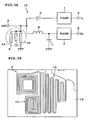
- Fig. 1A is a circuit diagram of a duplexer according to a first preferred embodiment of the present invention
- Fig. 1B is a plan view of open stubs of the duplexer
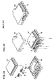
- Figs. 2A through 2C are external perspective views of the duplexer according to the first preferred embodiment, illustrating the assembly procedure.
- the duplexer includes an input terminal 4 to which a transmission (Tx) signal is input, an output terminal 5 from which a received (Rx) signal is output, and an antenna (ANT) terminal 3 defining a shared input/output terminal to which the transmission signal is input and from which the received signal is output.
- Tx transmission
- Rx received
- ANT antenna
- the duplexer further includes Tx-signal and Rx-signal band-pass filters (BPFs), which are defined by T-shaped ladder SAW filters each having series resonators on the input and output sides, respectively, namely, a Tx SAW filter 1 and an Rx SAW filter 2.
- BPFs band-pass filters
- the Tx SAW filter 1 is connected between the antenna terminal 3 and the input terminal 4.
- the Rx SAW filter 2 is connected between the antenna terminal 3 and the output terminal 5.
- the Tx SAW filter 1 and the Rx SAW filter 2 are preferably housed in a single package 18, as shown in Figs. 2A and 2B .
- the duplexer further includes a matching circuit 15 having a capacitor 6, which is connected between the antenna terminal 3 and the Tx SAW filter 1, and a first parallel capacitor 14, a series inductor 8, and a second parallel capacitor 7, which are connected between the antenna terminal 3 and the Rx SAW filter 2.
- the first parallel capacitor 14 is connected between the antenna terminal 3 and ground.
- the inductor 8 is connected between the antenna terminal 3 and the Rx SAW filter 2.
- the second parallel capacitor 7 is connected between the Rx SAW filter 2 and ground.
- the capacitor 6, the first parallel capacitor 14, the inductor 8, and the second parallel capacitor 7 define the matching circuit 15 for impedance matching.
- the matching circuit 15 is a circuit for matching impedance to the antenna terminal conditions. Specifically, the impedance matching circuit 15 performs impedance matching such that, at the passband frequencies of the Rx SAW filter 2, the impedance of the Tx SAW filter 1 is as open as possible and the impedance of the Rx SAW filter 2 matches the antenna terminal conditions as much as possible.
- the matching circuit 15 also performs impedance matching such that, at the passband frequencies of the Tx SAW filter 1, the impedance of the Rx SAW filter 2 is as open as possible and the impedance of the Tx SAW filter 1 matches the antenna terminal conditions as much as possible.
- the Tx SAW filter 1 of the duplexer must have a characteristic in which the attenuation poles are located in the passband of the Rx filter 2.
- the Rx SAW filter 2 must have a characteristic in which the attenuation poles are located in the passband of the Tx filter 1.
- the attenuation poles in the high-frequency range are used for attenuation in the passband of the Rx SAW filter 2.
- an attenuation pole for harmonic suppression cannot be used in the Tx SAW filter 1 and the Rx SAW filter 2 of the duplexer.
- One typical harmonic suppression approach is to add a trap circuit, but this is not desirable in view of size reduction.
- the first parallel capacitor 14 includes open stubs (trap circuits) 9 and 10, which are defined by microstrip lines, for providing attenuation poles at the frequencies at which the second and third harmonics of the Tx band occur, respectively.
- the open stubs 9 and 10 provide suppression of second and third harmonics of the Tx band, respectively.
- the open stub 9 suppresses a second harmonic and the open stub 10 suppresses a third harmonic, the open stubs 9 and 10 have different lengths, which are about one quarter wavelength ( ⁇ ) of the second and third harmonics, respectively.
- open stubs are capacitive in the frequency range lower than the resonance point and are inductive in the frequency range higher than the resonance point. Therefore, the open stubs 9 and 10 used for harmonic suppression are capacitive at the passband frequencies.
- a stub which is also referred to as a stub resonator, is a series resonator having zero impedance with the transmission line short-circuited at a length equal to an even-numbered multiple of ⁇ /4 (a short stub) or open at a length equal to an odd-numbered multiple of ⁇ /4 (an open stub), or a parallel resonator an impedance of ⁇ with the transmission line short-circuited at a length that is substantially equal to an odd-numbered multiple of ⁇ /4 or open at a length equal to an even-numbered multiple of ⁇ /4, where ⁇ indicates the wavelength of the frequency of the desired attenuation pole.
- the open stubs 9 and 10 are provided in a multi-layer substrate 12. Since the microstrip lines of the open stubs 9 and 10 are provided in a layer of the multi-layer substrate 12, the multi-layer substrate 12 having the open stubs 9 and 10 is only about 50 ⁇ m thicker than and has a cross-sectional area in the plane direction thereof (i.e., the occupied area) approximately the same as the multi-layer substrate 12 without the open stubs 9 and 10. Thus, the size of the multi-layer substrate 12 is not substantially increased.
- the open stubs 9 and 10 function as parallel capacitors in the passband, and the lengths of the open stubs 9 and 10 are adjusted so as to suppress the second and third harmonics of the Tx band, respectively.
- the capacitances of the open stubs 9 and 10 are therefore fixed.
- a parallel inductor 11 for capacitance control is connected between the antenna terminal 3 and ground to obtain the desired capacitance of the first parallel capacitor 14.
- the parallel inductor 11 is preferably a wound-type chip coil with a Q factor of at least about 20.
- the chip components are connected to each other via signal lines provided in advance on the mounting surface of the multi-layer substrate 12. After the components are mounted on the surface of the multi-layer substrate 12, a metal cover 20 is mounted on the multi-layer substrate 12 (see Fig.2B ) so as to cover the mounted components, thereby providing the duplexer according to the first preferred embodiment as shown in Fig.2C .
- the duplexer includes SAW filters, namely, the Tx SAW filter 1 and the Rx SAW filter 2, thus achieving size reduction.
- the matching circuit 15 is defined by the first parallel capacitor 14, the series inductor 8, and the second parallel capacitor 7, and the first parallel capacitor 14 is defined by the open stubs (trap circuits) 9 and 10 and the parallel inductor 11, thus achieving both harmonic suppression and electrostatic discharge (ESD) protection.
- a duplexer according to a second preferred embodiment of the present invention will now be described with reference to Figs. 3A through 4C .
- components having similar functions to those of the first preferred embodiment are given the same reference numerals, and a description thereof is omitted.
- the duplexer according to the second preferred embodiment includes a microstrip-line parallel inductor 16, in place of the parallel inductor 11 defined by a wound-type chip coil in the first preferred embodiment, as shown in Fig. 3A .
- the microstrip-line parallel inductor 16 which is short-circuited to ground is also referred to as a short stub, a half-wavelength line, or a short-circuited stub, and inherently attenuates a certain characteristic frequency.
- the parallel inductor 16 functions only as an inductor.
- short stubs are inductive at frequencies that are lower than the antiresonance point, capacitive at the frequencies from the antiresonance point to the resonance point, and inductive at frequencies that are higher than the resonance point.
- the length of the parallel inductor 16, which is a short stub is preferably arranged so as to be inductive in the passband of the Rx SAW filter 2.
- the microstrip line of the parallel inductor 16 is provided in, for example, the same layer of the multi-layer substrate 12 as the layer in which the open stubs 9 and 10 are provided.
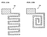
- the microstrip line of the parallel inductor 16 may have a meandering pattern or a spiral pattern, but preferably has a spiral pattern to reduce the size thereof.
- One end of such a patterned microstrip line is connected to a ground pattern provided on the reverse surface of the multi-layer substrate 12 via a through hole (not shown) provided in the multi-layer substrate 12 in the thickness direction thereof.
- the microstrip line of the parallel inductor 16 has a resonance point in a frequency range higher than the passband.
- the parallel inductor 16 has an inductance component in the passband.
- harmonic suppression and high surge resistance are achieved while reducing the number of mounted components.
- the parallel inductor 16 which controls capacitance is defined by a microstrip line
- the microstrip line can be built in the layered structure of the multi-layer substrate 12, and the parallel inductor 16 achieves advantages similar to the parallel inductor 11 of the first preferred embodiment mounted on the surface of the multi-layer substrate 12.
- the microstrip line of the parallel inductor 16 requires a smaller space, thus, reducing the size of the duplexer.
- the capacitor 6, the second parallel capacitor 7, the inductor 8, the Tx SAW filter 1, and the Rx SAW filter 2 are surface-mounted on the multi-layer substrate 12.
- These chip components are connected to each other via signal lines formed in advance on the mounting surface of the multi-layer substrate 12.
- a metal cover 22 is mounted on the multi-layer substrate 12 so as to cover the mounted components, thereby producing the duplexer of the second preferred embodiment (see Fig.4C ).
- each of the Tx SAW filter 1 and the Rx SAW filter 2 are housed in separate packages.
- the SAW filters 1 and 2 may be housed in a single package.
- each of the Tx SAW filter 1 and the Rx SAW filter 2, which are BPFs is preferably a T-shaped ladder SAW filter having series resonators on the input and output sides.
- each of the filters 1 and 2 may be a ⁇ -shaped ladder filter beginning with a parallel resonator.
- a communications apparatus such as a cellular phone, including the above-described duplexer suppresses harmonics from the Tx SAW filter 1 via the open stubs 9 and 10, which thus greatly improves the noise performance of the apparatus.
- the resonance points of the open stubs 9 and 10 are substantially adjusted for the wavelengths of the second and third harmonics, respectively, thereby suppressing harmonics or spurious components from a power amplifier or a SAW filter.
- the duplexer according to the first and second preferred embodiments of the present invention has higher surge resistance than the duplexer of the comparative example, and provides higher electrical durability of the device, such as a cellular phone.
- the parallel inductor 11 or 16 is preferably connected between the antenna and the Tx (or Rx) side, thus permitting an incoming electrostatic surge current from the antenna to escape to ground via the parallel inductor 11 or 16. The surge current is prevented from reaching the SAW filter, and the surge resistance greatly increases.
- T-shaped ladder SAW filters are preferably used in the first and second preferred embodiments, a voltage applied to one resonator is dispersed, thus improving the surge resistance.
- the duplexer of preferred embodiments of the present invention requires fewer components than a duplexer in which all the capacitors and inductors of the matching circuit 15 are defined by chips, because the open stubs 9 and 10 function as parallel capacitors in the passband, thus eliminating the need for a traditional parallel capacitor defined by a chip, such as a multi-layer capacitor.
- the capacitance generated by the open stubs 9 and 10 is controlled by the mounted parallel inductor. Therefore, the number of required components is not increased.
- the insertion loss of the duplexer of preferred embodiments of the present invention was measured when the Q factor of the parallel inductor varied in a range of about 1 to about 100. The results are shown in Figs. 7 and 8 . It was found that the Q factor of the parallel inductor was preferably at least about 20. Generally, wound-type chip coil components have a higher Q factor than microstrip-line inductors. Therefore, it is more beneficial that the parallel inductor be defined by a wound-type chip coil component in view of the minimal degradation of the insertion loss of the duplexer.
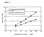
- Fig. 9 shows the relationship between the inductance and the microstrip line length when the microstrip line of the duplexer is a meandering microstrip line 32 shown in Fig. 10A and when the microstrip line is a spiral microstrip line 34 shown in Fig. 10B .
- the spiral microstrip line 34 has a shorter pattern length than the meandering microstrip line 32, and thus, requires a smaller space.
- spiral microstrip line 34 In the spiral microstrip line 34, a signal flows in adjacent line portions in the same direction, thus making it difficult to cancel the magnetic fields generated by the current. In the meandering microstrip line 32, on the other hand, a signal flows in adjacent line portions in opposite directions, thus, making it possible to easily cancel the magnetic fields generated by the current.
- the spiral microstrip line 34 generates lower magnetic coupling, and has lower inductance loss caused by the magnetic coupling. Therefore, the spiral microstrip line 34 has a shorter pattern length.
- an attenuation pole is defined by an open stub.
- the duplexer disclosed in that publication includes a matching circuit having a different structure from that of the present invention.
Landscapes
- Physics & Mathematics (AREA)
- Acoustics & Sound (AREA)
- Engineering & Computer Science (AREA)
- Computer Networks & Wireless Communication (AREA)
- Signal Processing (AREA)
- Surface Acoustic Wave Elements And Circuit Networks Thereof (AREA)
- Transceivers (AREA)
- Control Of Motors That Do Not Use Commutators (AREA)
Claims (13)
- Duplexeur comprenant :un filtre de transmission (1) et un filtre de réception (2) qui sont connectés en parallèle à une borne d'antenne (3) ; etun circuit d'adaptation (15) prévu entre la borne d'antenne (3) et au moins l'un du filtre de transmission (1) et du filtre de réception (2),caractérisé en ce que :le filtre de transmission (1) et le filtre de réception (2) comprennent chacun un filtre à onde acoustique de surface ;le circuit d'adaptation comprend un premier dispositif formant condensateur parallèle (14) connecté à la borne d'antenne (3), où le premier dispositif formant condensateur parallèle (14) comprend, en tant que circuit réjecteur, au moins un bras de réactance en circuit ouvert (9/10) correspondant à une harmonique à supprimer, et le premier dispositif formant condensateur parallèle (14) comprend une inductance parallèle (11) connectée entre la borne d'antenne (3) et la terre ; etle bras de réactance en circuit ouvert (9/10) est capacitif et la réactance combinée du bras de réactance en circuit ouvert (9/10) et de l'inductance parallèle (11) est capacitive dans la bande passante du filtre de transmission (1) et du filtre de réception (2).
- Duplexeur selon la revendication 1, dans lequel le circuit d'adaptation (15) comprend une inductance série (8) et un deuxième condensateur parallèle (7), et une première extrémité de l'inductance série (8) est connectée à la borne d'antenne (3) et une deuxième extrémité de l'inductance série (8) est connectée au deuxième condensateur parallèle (7).
- Duplexeur selon la revendication 1 ou 2, dans lequel l'inductance parallèle (11) a un facteur Q d'au moins environ 20.
- Duplexeur selon l'une quelconque des revendications précédentes, comprenant en outre :au moins un boîtier pour loger au moins l'un du filtre de transmission (1) et du filtre de réception (2) ; etun substrat multicouche (12) sur lequel est monté le boîtier et une partie du circuit d'adaptation (15).
- Duplexeur selon la revendication 4, dans lequel le bras de réactance en circuit ouvert (9/10) est formé dans le substrat multicouche (12).
- Duplexeur selon la revendication 4 ou 5, dans lequel l'inductance parallèle (11) du circuit d'adaptation (15) comprend une inductance-pastille.
- Duplexeur selon la revendication 4 ou 5, dans lequel l'inductance parallèle (11) du circuit d'adaptation (15) comprend un bras de réactance court qui est formé dans le substrat multicouche (12).
- Duplexeur selon la revendication 1, comprenant en outre un boîtier pour loger le filtre de transmission (1) et le filtre de réception (2), où le boîtier loge également le circuit d'adaptation (15).
- Duplexeur selon la revendication 7, dans lequel l'inductance parallèle (11) du circuit d'adaptation (15) comprend une ligne microbande en spirale (34).
- Duplexeur selon l'une quelconque des revendications précédentes, dans lequel le filtre de transmission (1) comprend un filtre SAW de type récurrent, ayant un premier résonateur SAW série connecté du côté de l'antenne.
- Duplexeur selon la revendication 1, dans lequel l'inductance parallèle (11) est une inductance-pastille de type bobiné.
- Duplexeur selon la revendication 10, dans lequel le filtre SAW de type récurrent est un filtre SAW récurrent en T.
- Appareil de communication comprenant le duplexeur selon l'une quelconque des revendications précédentes.
Applications Claiming Priority (2)
| Application Number | Priority Date | Filing Date | Title |
|---|---|---|---|
| JP2002365968 | 2002-12-18 | ||
| JP2002365968A JP3972810B2 (ja) | 2002-12-18 | 2002-12-18 | 分波器、および通信機 |
Publications (2)
| Publication Number | Publication Date |
|---|---|
| EP1432133A1 EP1432133A1 (fr) | 2004-06-23 |
| EP1432133B1 true EP1432133B1 (fr) | 2010-07-21 |
Family
ID=32376253
Family Applications (1)
| Application Number | Title | Priority Date | Filing Date |
|---|---|---|---|
| EP03293198A Expired - Lifetime EP1432133B1 (fr) | 2002-12-18 | 2003-12-17 | Duplexeur et dispositif de communication |
Country Status (7)
| Country | Link |
|---|---|
| US (1) | US6982612B2 (fr) |
| EP (1) | EP1432133B1 (fr) |
| JP (1) | JP3972810B2 (fr) |
| KR (1) | KR100598433B1 (fr) |
| CN (1) | CN1317793C (fr) |
| AT (1) | ATE475226T1 (fr) |
| DE (1) | DE60333431D1 (fr) |
Families Citing this family (43)
| Publication number | Priority date | Publication date | Assignee | Title |
|---|---|---|---|---|
| JP4096845B2 (ja) * | 2002-11-08 | 2008-06-04 | 株式会社村田製作所 | 分波器および通信装置 |
| JP3839001B2 (ja) * | 2003-07-28 | 2006-11-01 | 埼玉日本電気株式会社 | 携帯無線機 |
| JP2005268878A (ja) * | 2004-03-16 | 2005-09-29 | Matsushita Electric Ind Co Ltd | アンテナ共用器 |
| ATE434291T1 (de) * | 2004-03-30 | 2009-07-15 | Tdk Corp | Diplexer- und anpass-schaltung |
| KR100617138B1 (ko) * | 2004-12-02 | 2006-08-31 | 엘지전자 주식회사 | 모바일 스위치가 내장된 듀플렉서 모듈 및 이를 이용한이동 통신 단말기 |
| JP5059013B2 (ja) * | 2005-10-17 | 2012-10-24 | サムスン エレクトロニクス カンパニー リミテッド | 多重ユーザ多重アンテナ通信システムの送・受信機及び送・受信方法 |
| CN100574004C (zh) * | 2005-11-11 | 2009-12-23 | 中国科学院上海微系统与信息技术研究所 | 补偿型螺旋微带谐振单元及其构成的环形耦合器 |
| DE102006005298B4 (de) * | 2006-02-06 | 2017-05-24 | Epcos Ag | Duplexer |
| EP2031755B1 (fr) * | 2006-06-12 | 2013-11-20 | Murata Manufacturing Co. Ltd. | Démultiplexeur d'ondes |
| DE102006031548A1 (de) * | 2006-07-07 | 2008-01-17 | Epcos Ag | Sendeempfangsschaltung |
| WO2008029641A1 (fr) * | 2006-08-30 | 2008-03-13 | Kyocera Corporation | Carte de circuit pour dispositif séparateur d'onde, séparateur d'onde et dispositif de communication |
| JP4345850B2 (ja) | 2006-09-11 | 2009-10-14 | ソニー株式会社 | 通信システム及び通信装置 |
| EP1926223B1 (fr) | 2006-11-21 | 2018-02-28 | Sony Corporation | Système et appareil de communication |
| JP4843467B2 (ja) * | 2006-11-22 | 2011-12-21 | Necトーキン株式会社 | 高表面インピーダンス構造体、アンテナ装置、及びrfidタグ |
| JP5038740B2 (ja) * | 2007-02-23 | 2012-10-03 | パナソニック株式会社 | 帯域通過フィルタおよびその製造方法 |
| JP4823943B2 (ja) * | 2007-03-06 | 2011-11-24 | 均 北吉 | 無線タグ、無線タグリーダ及びパルス符号化鍵検出回路とそれらを用いた無線タグシステム |
| JP5183459B2 (ja) * | 2008-12-26 | 2013-04-17 | 太陽誘電株式会社 | 分波器、分波器用基板および電子装置 |
| US8289910B2 (en) * | 2009-04-24 | 2012-10-16 | Kathrein-Werke Kg | Device for receiving and transmitting mobile telephony signals with multiple transmit-receive branches |
| KR101714040B1 (ko) * | 2010-07-06 | 2017-03-08 | 엘지이노텍 주식회사 | 안테나 임피던스 모니터링 시스템 |
| RU2597325C2 (ru) * | 2011-01-14 | 2016-09-10 | Конинклейке Филипс Электроникс Н.В. | Система радиоприемника с разнесением |
| US9391650B2 (en) * | 2011-02-11 | 2016-07-12 | Qualcomm Incorporated | Front-end RF filters with embedded impedance transformation |
| TWI474633B (zh) | 2011-12-16 | 2015-02-21 | Richwave Technology Corp | 具靜電保護機制之整合被動元件 |
| KR101447075B1 (ko) | 2012-12-21 | 2014-10-06 | 전자부품연구원 | 다이플렉서와 정합회로를 이용한 듀플렉서 |
| JP6380400B2 (ja) * | 2013-09-26 | 2018-08-29 | 株式会社村田製作所 | 周波数可変フィルタ |
| JP6395638B2 (ja) * | 2015-02-24 | 2018-09-26 | 古河電気工業株式会社 | 無線装置 |
| JP5999295B1 (ja) * | 2015-04-01 | 2016-09-28 | 株式会社村田製作所 | デュプレクサ |
| CN107735948B (zh) * | 2015-06-24 | 2019-01-04 | 株式会社村田制作所 | 多工器、发送装置、接收装置、高频前端电路、通信装置以及多工器的阻抗匹配方法 |
| KR101991219B1 (ko) * | 2016-05-19 | 2019-06-19 | 가부시키가이샤 무라타 세이사쿠쇼 | 필터 장치 |
| JP6690608B2 (ja) * | 2017-07-20 | 2020-04-28 | 株式会社村田製作所 | マルチプレクサ、高周波フロントエンド回路および通信装置 |
| KR102046345B1 (ko) * | 2017-07-31 | 2019-11-19 | 가부시키가이샤 무라타 세이사쿠쇼 | 분파기 및 프론트엔드 회로 |
| CN107483073B (zh) * | 2017-09-08 | 2021-04-23 | 台州市吉吉知识产权运营有限公司 | 一种射频匹配电路和射频系统 |
| JP7055006B2 (ja) * | 2017-11-29 | 2022-04-15 | キヤノン株式会社 | 分岐回路 |
| DE102018102832B4 (de) * | 2018-02-08 | 2023-01-05 | RF360 Europe GmbH | Filterschaltung mit einem Notchfilter |
| JP6930463B2 (ja) * | 2018-03-08 | 2021-09-01 | 株式会社村田製作所 | マルチプレクサ、および、通信装置 |
| DE102019210495A1 (de) | 2018-07-18 | 2020-01-23 | Skyworks Solutions, Inc. | Paralleles akustisches hybridpassivfilter |
| CN111602288B (zh) | 2018-08-06 | 2021-04-16 | 株式会社村田制作所 | 电路基板、电路基板模块以及天线模块 |
| US20200112920A1 (en) * | 2018-10-05 | 2020-04-09 | California Eastern Laboratories, Inc. | Compliant radio and method of use |
| JP6919664B2 (ja) * | 2019-01-31 | 2021-08-18 | 株式会社村田製作所 | マルチプレクサおよび通信装置 |
| CN110350272A (zh) * | 2019-07-02 | 2019-10-18 | 湖南赛博诺格电子科技有限公司 | 一种传输型小型化90°移相器 |
| CN110600839B (zh) | 2019-09-18 | 2021-09-21 | 京东方科技集团股份有限公司 | 控制基板、液晶移相器及控制基板的制作方法 |
| US11818836B2 (en) | 2020-02-03 | 2023-11-14 | Commscope Technologies Llc | Systems for electrostatic discharge protection |
| US11309860B1 (en) * | 2020-10-09 | 2022-04-19 | Apple Inc. | Single ladder duplexer with impedance gradient |
| DE102021202319A1 (de) | 2021-03-04 | 2022-09-08 | Continental Automotive Technologies GmbH | Antennenanordnung für einen elektronischen Fahrzeugschlüssel |
Family Cites Families (14)
| Publication number | Priority date | Publication date | Assignee | Title |
|---|---|---|---|---|
| US5023866A (en) | 1987-02-27 | 1991-06-11 | Motorola, Inc. | Duplexer filter having harmonic rejection to control flyback |
| US5095285A (en) * | 1990-08-31 | 1992-03-10 | Texas Instruments Incorporated | Monolithically realizable harmonic trapping circuit |
| JPH066111A (ja) | 1992-06-18 | 1994-01-14 | Mitsubishi Electric Corp | 複合デュプレックスフィルタ |
| GB2271487B (en) | 1992-10-09 | 1995-08-02 | Maxon Systems Inc | Single antenna transmitter/receiver |
| JPH06350307A (ja) | 1993-06-03 | 1994-12-22 | Fuji Elelctrochem Co Ltd | 分波器 |
| JPH07226607A (ja) | 1994-02-10 | 1995-08-22 | Hitachi Ltd | 分波器、分波器モジュールおよび無線通信装置 |
| JPH11312907A (ja) * | 1997-12-18 | 1999-11-09 | Matsushita Electric Ind Co Ltd | 整合回路チップ、整合回路付きフィルタ、共用器、及び移動体通信機器 |
| US5939939A (en) * | 1998-02-27 | 1999-08-17 | Motorola, Inc. | Power combiner with harmonic selectivity |
| JP2001127663A (ja) | 1999-10-29 | 2001-05-11 | Ngk Spark Plug Co Ltd | 静電気保護回路 |
| JP2001313542A (ja) * | 2000-04-28 | 2001-11-09 | Oki Electric Ind Co Ltd | 分波器 |
| JP2001352271A (ja) | 2000-06-09 | 2001-12-21 | Hitachi Metals Ltd | 高周波スイッチモジュール |
| US6577199B2 (en) * | 2000-12-07 | 2003-06-10 | Ericsson, Inc. | Harmonic matching network for a saturated amplifier |
| TW486861B (en) * | 2001-07-04 | 2002-05-11 | Ind Tech Res Inst | Impedance matching circuit for a multi-band power amplifier |
| JP3900013B2 (ja) * | 2001-07-30 | 2007-04-04 | 株式会社村田製作所 | 弾性表面波分波器、通信装置 |
-
2002
- 2002-12-18 JP JP2002365968A patent/JP3972810B2/ja not_active Expired - Lifetime
-
2003
- 2003-12-02 US US10/725,877 patent/US6982612B2/en not_active Expired - Lifetime
- 2003-12-08 CN CNB2003101201512A patent/CN1317793C/zh not_active Expired - Lifetime
- 2003-12-15 KR KR1020030091192A patent/KR100598433B1/ko active IP Right Grant
- 2003-12-17 EP EP03293198A patent/EP1432133B1/fr not_active Expired - Lifetime
- 2003-12-17 AT AT03293198T patent/ATE475226T1/de not_active IP Right Cessation
- 2003-12-17 DE DE60333431T patent/DE60333431D1/de not_active Expired - Lifetime
Also Published As
| Publication number | Publication date |
|---|---|
| US6982612B2 (en) | 2006-01-03 |
| KR100598433B1 (ko) | 2006-07-11 |
| JP2004200941A (ja) | 2004-07-15 |
| KR20040054506A (ko) | 2004-06-25 |
| CN1508903A (zh) | 2004-06-30 |
| DE60333431D1 (de) | 2010-09-02 |
| JP3972810B2 (ja) | 2007-09-05 |
| US20040119562A1 (en) | 2004-06-24 |
| CN1317793C (zh) | 2007-05-23 |
| EP1432133A1 (fr) | 2004-06-23 |
| ATE475226T1 (de) | 2010-08-15 |
Similar Documents
| Publication | Publication Date | Title |
|---|---|---|
| EP1432133B1 (fr) | Duplexeur et dispositif de communication | |
| KR101116941B1 (ko) | 필터, 듀플렉서, 통신 모듈 | |
| JP5463669B2 (ja) | 分波回路、高周波回路及び高周波モジュール | |
| KR100906356B1 (ko) | 하이 패스 필터 | |
| EP1253713B1 (fr) | Réglage des coefficients de couplage effectifs pour résonateurs acoustiques à ondes de volume | |
| US7339445B2 (en) | BAW duplexer without phase shifter | |
| US6756864B2 (en) | Branching filter and communication apparatus | |
| US7646265B2 (en) | BAW resonator filter bandwidth and out-of-band frequency rejection | |
| EP2141805B1 (fr) | Dispositif de résonateur, filtre l'incluant, et duplexeur | |
| JP3487692B2 (ja) | 分波器 | |
| US7579927B2 (en) | Duplexer | |
| EP2093881B1 (fr) | Dispositif de filtre d'onde élastique | |
| EP1758247A2 (fr) | Duplexeur avec circuit d'adaptation | |
| JP2001024476A (ja) | 送受切換器 | |
| US20050073375A1 (en) | Single chip-type film bulk acoustic resonator duplexer | |
| US6972641B2 (en) | FBAR ladder filter and method of grounding of FBAR ladder filters | |
| JPH06350307A (ja) | 分波器 | |
| CN115955213A (zh) | 一种提升带外远端多倍频抑制的双工器 | |
| CN212305276U (zh) | 带通滤波器和滤波器 | |
| US20050046512A1 (en) | Demultiplexer | |
| CN113067561A (zh) | 带阻滤波器与多频带阻滤波器 | |
| CN112491384A (zh) | 一种fbar滤波器电路 | |
| JP6406482B1 (ja) | トラップフィルタおよびフィルタ回路 | |
| US20230283260A1 (en) | Notch filter and multi-frequency notch filter | |
| KR20220131671A (ko) | 필터 장치 및 saw 필터 |
Legal Events
| Date | Code | Title | Description |
|---|---|---|---|
| PUAI | Public reference made under article 153(3) epc to a published international application that has entered the european phase |
Free format text: ORIGINAL CODE: 0009012 |
|
| 17P | Request for examination filed |
Effective date: 20031230 |
|
| AK | Designated contracting states |
Kind code of ref document: A1 Designated state(s): AT BE BG CH CY CZ DE DK EE ES FI FR GB GR HU IE IT LI LU MC NL PT RO SE SI SK TR |
|
| AX | Request for extension of the european patent |
Extension state: AL LT LV MK |
|
| AKX | Designation fees paid |
Designated state(s): AT BE BG CH CY CZ DE DK EE ES FI FR GB GR HU IE IT LI LU MC NL PT RO SE SI SK TR |
|
| 17Q | First examination report despatched |
Effective date: 20070611 |
|
| RAP1 | Party data changed (applicant data changed or rights of an application transferred) |
Owner name: MURATA MANUFACTURING CO., LTD. |
|
| GRAP | Despatch of communication of intention to grant a patent |
Free format text: ORIGINAL CODE: EPIDOSNIGR1 |
|
| GRAS | Grant fee paid |
Free format text: ORIGINAL CODE: EPIDOSNIGR3 |
|
| GRAA | (expected) grant |
Free format text: ORIGINAL CODE: 0009210 |
|
| AK | Designated contracting states |
Kind code of ref document: B1 Designated state(s): AT BE BG CH CY CZ DE DK EE ES FI FR GB GR HU IE IT LI LU MC NL PT RO SE SI SK TR |
|
| REG | Reference to a national code |
Ref country code: GB Ref legal event code: FG4D |
|
| REG | Reference to a national code |
Ref country code: CH Ref legal event code: EP |
|
| REG | Reference to a national code |
Ref country code: IE Ref legal event code: FG4D |
|
| REF | Corresponds to: |
Ref document number: 60333431 Country of ref document: DE Date of ref document: 20100902 Kind code of ref document: P |
|
| REG | Reference to a national code |
Ref country code: NL Ref legal event code: VDEP Effective date: 20100721 |
|
| PG25 | Lapsed in a contracting state [announced via postgrant information from national office to epo] |
Ref country code: FI Free format text: LAPSE BECAUSE OF FAILURE TO SUBMIT A TRANSLATION OF THE DESCRIPTION OR TO PAY THE FEE WITHIN THE PRESCRIBED TIME-LIMIT Effective date: 20100721 Ref country code: AT Free format text: LAPSE BECAUSE OF FAILURE TO SUBMIT A TRANSLATION OF THE DESCRIPTION OR TO PAY THE FEE WITHIN THE PRESCRIBED TIME-LIMIT Effective date: 20100721 Ref country code: NL Free format text: LAPSE BECAUSE OF FAILURE TO SUBMIT A TRANSLATION OF THE DESCRIPTION OR TO PAY THE FEE WITHIN THE PRESCRIBED TIME-LIMIT Effective date: 20100721 |
|
| PG25 | Lapsed in a contracting state [announced via postgrant information from national office to epo] |
Ref country code: SI Free format text: LAPSE BECAUSE OF FAILURE TO SUBMIT A TRANSLATION OF THE DESCRIPTION OR TO PAY THE FEE WITHIN THE PRESCRIBED TIME-LIMIT Effective date: 20100721 Ref country code: BG Free format text: LAPSE BECAUSE OF FAILURE TO SUBMIT A TRANSLATION OF THE DESCRIPTION OR TO PAY THE FEE WITHIN THE PRESCRIBED TIME-LIMIT Effective date: 20101021 Ref country code: CY Free format text: LAPSE BECAUSE OF FAILURE TO SUBMIT A TRANSLATION OF THE DESCRIPTION OR TO PAY THE FEE WITHIN THE PRESCRIBED TIME-LIMIT Effective date: 20100721 Ref country code: PT Free format text: LAPSE BECAUSE OF FAILURE TO SUBMIT A TRANSLATION OF THE DESCRIPTION OR TO PAY THE FEE WITHIN THE PRESCRIBED TIME-LIMIT Effective date: 20101122 |
|
| PG25 | Lapsed in a contracting state [announced via postgrant information from national office to epo] |
Ref country code: SE Free format text: LAPSE BECAUSE OF FAILURE TO SUBMIT A TRANSLATION OF THE DESCRIPTION OR TO PAY THE FEE WITHIN THE PRESCRIBED TIME-LIMIT Effective date: 20100721 Ref country code: GR Free format text: LAPSE BECAUSE OF FAILURE TO SUBMIT A TRANSLATION OF THE DESCRIPTION OR TO PAY THE FEE WITHIN THE PRESCRIBED TIME-LIMIT Effective date: 20101022 Ref country code: BE Free format text: LAPSE BECAUSE OF FAILURE TO SUBMIT A TRANSLATION OF THE DESCRIPTION OR TO PAY THE FEE WITHIN THE PRESCRIBED TIME-LIMIT Effective date: 20100721 |
|
| PG25 | Lapsed in a contracting state [announced via postgrant information from national office to epo] |
Ref country code: DK Free format text: LAPSE BECAUSE OF FAILURE TO SUBMIT A TRANSLATION OF THE DESCRIPTION OR TO PAY THE FEE WITHIN THE PRESCRIBED TIME-LIMIT Effective date: 20100721 |
|
| PLBE | No opposition filed within time limit |
Free format text: ORIGINAL CODE: 0009261 |
|
| STAA | Information on the status of an ep patent application or granted ep patent |
Free format text: STATUS: NO OPPOSITION FILED WITHIN TIME LIMIT |
|
| PG25 | Lapsed in a contracting state [announced via postgrant information from national office to epo] |
Ref country code: CZ Free format text: LAPSE BECAUSE OF FAILURE TO SUBMIT A TRANSLATION OF THE DESCRIPTION OR TO PAY THE FEE WITHIN THE PRESCRIBED TIME-LIMIT Effective date: 20100721 Ref country code: RO Free format text: LAPSE BECAUSE OF FAILURE TO SUBMIT A TRANSLATION OF THE DESCRIPTION OR TO PAY THE FEE WITHIN THE PRESCRIBED TIME-LIMIT Effective date: 20100721 Ref country code: IT Free format text: LAPSE BECAUSE OF FAILURE TO SUBMIT A TRANSLATION OF THE DESCRIPTION OR TO PAY THE FEE WITHIN THE PRESCRIBED TIME-LIMIT Effective date: 20100721 Ref country code: SK Free format text: LAPSE BECAUSE OF FAILURE TO SUBMIT A TRANSLATION OF THE DESCRIPTION OR TO PAY THE FEE WITHIN THE PRESCRIBED TIME-LIMIT Effective date: 20100721 Ref country code: EE Free format text: LAPSE BECAUSE OF FAILURE TO SUBMIT A TRANSLATION OF THE DESCRIPTION OR TO PAY THE FEE WITHIN THE PRESCRIBED TIME-LIMIT Effective date: 20100721 |
|
| 26N | No opposition filed |
Effective date: 20110426 |
|
| PG25 | Lapsed in a contracting state [announced via postgrant information from national office to epo] |
Ref country code: ES Free format text: LAPSE BECAUSE OF FAILURE TO SUBMIT A TRANSLATION OF THE DESCRIPTION OR TO PAY THE FEE WITHIN THE PRESCRIBED TIME-LIMIT Effective date: 20101101 |
|
| PG25 | Lapsed in a contracting state [announced via postgrant information from national office to epo] |
Ref country code: MC Free format text: LAPSE BECAUSE OF NON-PAYMENT OF DUE FEES Effective date: 20101231 |
|
| REG | Reference to a national code |
Ref country code: CH Ref legal event code: PL |
|
| REG | Reference to a national code |
Ref country code: DE Ref legal event code: R097 Ref document number: 60333431 Country of ref document: DE Effective date: 20110426 |
|
| GBPC | Gb: european patent ceased through non-payment of renewal fee |
Effective date: 20101217 |
|
| REG | Reference to a national code |
Ref country code: FR Ref legal event code: ST Effective date: 20110831 |
|
| PG25 | Lapsed in a contracting state [announced via postgrant information from national office to epo] |
Ref country code: IE Free format text: LAPSE BECAUSE OF NON-PAYMENT OF DUE FEES Effective date: 20101217 Ref country code: FR Free format text: LAPSE BECAUSE OF NON-PAYMENT OF DUE FEES Effective date: 20110103 Ref country code: LI Free format text: LAPSE BECAUSE OF NON-PAYMENT OF DUE FEES Effective date: 20101231 Ref country code: CH Free format text: LAPSE BECAUSE OF NON-PAYMENT OF DUE FEES Effective date: 20101231 |
|
| PG25 | Lapsed in a contracting state [announced via postgrant information from national office to epo] |
Ref country code: GB Free format text: LAPSE BECAUSE OF NON-PAYMENT OF DUE FEES Effective date: 20101217 |
|
| PG25 | Lapsed in a contracting state [announced via postgrant information from national office to epo] |
Ref country code: LU Free format text: LAPSE BECAUSE OF NON-PAYMENT OF DUE FEES Effective date: 20101217 Ref country code: HU Free format text: LAPSE BECAUSE OF FAILURE TO SUBMIT A TRANSLATION OF THE DESCRIPTION OR TO PAY THE FEE WITHIN THE PRESCRIBED TIME-LIMIT Effective date: 20110122 |
|
| PG25 | Lapsed in a contracting state [announced via postgrant information from national office to epo] |
Ref country code: TR Free format text: LAPSE BECAUSE OF FAILURE TO SUBMIT A TRANSLATION OF THE DESCRIPTION OR TO PAY THE FEE WITHIN THE PRESCRIBED TIME-LIMIT Effective date: 20100721 |
|
| PGFP | Annual fee paid to national office [announced via postgrant information from national office to epo] |
Ref country code: DE Payment date: 20221213 Year of fee payment: 20 |
|
| REG | Reference to a national code |
Ref country code: DE Ref legal event code: R071 Ref document number: 60333431 Country of ref document: DE |