EP1418618A2 - Vefahren zur Herstellung von Höhlen zwischen Multischichtmetallisierungen - Google Patents
Vefahren zur Herstellung von Höhlen zwischen Multischichtmetallisierungen Download PDFInfo
- Publication number
- EP1418618A2 EP1418618A2 EP03024703A EP03024703A EP1418618A2 EP 1418618 A2 EP1418618 A2 EP 1418618A2 EP 03024703 A EP03024703 A EP 03024703A EP 03024703 A EP03024703 A EP 03024703A EP 1418618 A2 EP1418618 A2 EP 1418618A2
- Authority
- EP
- European Patent Office
- Prior art keywords
- cavity
- polyamic acid
- polyimide
- alicyclic
- wirings
- Prior art date
- Legal status (The legal status is an assumption and is not a legal conclusion. Google has not performed a legal analysis and makes no representation as to the accuracy of the status listed.)
- Granted
Links
Images
Classifications
-
- H—ELECTRICITY
- H10—SEMICONDUCTOR DEVICES; ELECTRIC SOLID-STATE DEVICES NOT OTHERWISE PROVIDED FOR
- H10W—GENERIC PACKAGES, INTERCONNECTIONS, CONNECTORS OR OTHER CONSTRUCTIONAL DETAILS OF DEVICES COVERED BY CLASS H10
- H10W20/00—Interconnections in chips, wafers or substrates
- H10W20/01—Manufacture or treatment
-
- H—ELECTRICITY
- H10—SEMICONDUCTOR DEVICES; ELECTRIC SOLID-STATE DEVICES NOT OTHERWISE PROVIDED FOR
- H10W—GENERIC PACKAGES, INTERCONNECTIONS, CONNECTORS OR OTHER CONSTRUCTIONAL DETAILS OF DEVICES COVERED BY CLASS H10
- H10W10/00—Isolation regions in semiconductor bodies between components of integrated devices
- H10W10/01—Manufacture or treatment
- H10W10/021—Manufacture or treatment of air gaps
-
- H—ELECTRICITY
- H10—SEMICONDUCTOR DEVICES; ELECTRIC SOLID-STATE DEVICES NOT OTHERWISE PROVIDED FOR
- H10W—GENERIC PACKAGES, INTERCONNECTIONS, CONNECTORS OR OTHER CONSTRUCTIONAL DETAILS OF DEVICES COVERED BY CLASS H10
- H10W10/00—Isolation regions in semiconductor bodies between components of integrated devices
- H10W10/20—Air gaps
-
- H—ELECTRICITY
- H10—SEMICONDUCTOR DEVICES; ELECTRIC SOLID-STATE DEVICES NOT OTHERWISE PROVIDED FOR
- H10W—GENERIC PACKAGES, INTERCONNECTIONS, CONNECTORS OR OTHER CONSTRUCTIONAL DETAILS OF DEVICES COVERED BY CLASS H10
- H10W20/00—Interconnections in chips, wafers or substrates
- H10W20/01—Manufacture or treatment
- H10W20/071—Manufacture or treatment of dielectric parts thereof
- H10W20/072—Manufacture or treatment of dielectric parts thereof of dielectric parts comprising air gaps
-
- H—ELECTRICITY
- H10—SEMICONDUCTOR DEVICES; ELECTRIC SOLID-STATE DEVICES NOT OTHERWISE PROVIDED FOR
- H10W—GENERIC PACKAGES, INTERCONNECTIONS, CONNECTORS OR OTHER CONSTRUCTIONAL DETAILS OF DEVICES COVERED BY CLASS H10
- H10W20/00—Interconnections in chips, wafers or substrates
- H10W20/40—Interconnections external to wafers or substrates, e.g. back-end-of-line [BEOL] metallisations or vias connecting to gate electrodes
- H10W20/45—Interconnections external to wafers or substrates, e.g. back-end-of-line [BEOL] metallisations or vias connecting to gate electrodes characterised by their insulating parts
- H10W20/46—Interconnections external to wafers or substrates, e.g. back-end-of-line [BEOL] metallisations or vias connecting to gate electrodes characterised by their insulating parts comprising air gaps
-
- H—ELECTRICITY
- H10—SEMICONDUCTOR DEVICES; ELECTRIC SOLID-STATE DEVICES NOT OTHERWISE PROVIDED FOR
- H10W—GENERIC PACKAGES, INTERCONNECTIONS, CONNECTORS OR OTHER CONSTRUCTIONAL DETAILS OF DEVICES COVERED BY CLASS H10
- H10W20/00—Interconnections in chips, wafers or substrates
- H10W20/40—Interconnections external to wafers or substrates, e.g. back-end-of-line [BEOL] metallisations or vias connecting to gate electrodes
- H10W20/45—Interconnections external to wafers or substrates, e.g. back-end-of-line [BEOL] metallisations or vias connecting to gate electrodes characterised by their insulating parts
- H10W20/48—Insulating materials thereof
-
- H—ELECTRICITY
- H10—SEMICONDUCTOR DEVICES; ELECTRIC SOLID-STATE DEVICES NOT OTHERWISE PROVIDED FOR
- H10W—GENERIC PACKAGES, INTERCONNECTIONS, CONNECTORS OR OTHER CONSTRUCTIONAL DETAILS OF DEVICES COVERED BY CLASS H10
- H10W20/00—Interconnections in chips, wafers or substrates
- H10W20/40—Interconnections external to wafers or substrates, e.g. back-end-of-line [BEOL] metallisations or vias connecting to gate electrodes
- H10W20/495—Capacitive arrangements or effects of, or between wiring layers
-
- H—ELECTRICITY
- H10—SEMICONDUCTOR DEVICES; ELECTRIC SOLID-STATE DEVICES NOT OTHERWISE PROVIDED FOR
- H10W—GENERIC PACKAGES, INTERCONNECTIONS, CONNECTORS OR OTHER CONSTRUCTIONAL DETAILS OF DEVICES COVERED BY CLASS H10
- H10W20/00—Interconnections in chips, wafers or substrates
- H10W20/40—Interconnections external to wafers or substrates, e.g. back-end-of-line [BEOL] metallisations or vias connecting to gate electrodes
- H10W20/482—Interconnections external to wafers or substrates, e.g. back-end-of-line [BEOL] metallisations or vias connecting to gate electrodes for individual devices provided for in groups H10D8/00 - H10D48/00, e.g. for power transistors
- H10W20/483—Interconnections over air gaps, e.g. air bridges
Definitions
- the present invention relates to a method of forming a cavity between wirings using a heat decomposable alicyclic polymer that is a polyamic acid and/or a polyimide obtained by reacting a specific alicyclic tetracarboxylic acid dianhydride and a specific alicyclic diamine, reveals a specific heat resistant temperature and a specific heat decomposition temperature, and can readily form a cavity structure between metallic wirings in, for example, semiconductors.
- a heat decomposable alicyclic polymer that is a polyamic acid and/or a polyimide obtained by reacting a specific alicyclic tetracarboxylic acid dianhydride and a specific alicyclic diamine, reveals a specific heat resistant temperature and a specific heat decomposition temperature, and can readily form a cavity structure between metallic wirings in, for example, semiconductors.
- silica (SiO 2 ) films formed by the vacuum process such as the CVD process have widely been employed as a dielectric film in semiconductors, etc.
- coating type dielectric films containing a tetraalkoxysilane hydrolyzate as the major component and called an SOG (Spin on Glass) film are employed mainly for the purpose of flattening.
- SOG Spin on Glass
- an object of the present invention is to provide a method that can readily form a cavity structure between metallic wirings in, for example, semiconductors using a polyamic acid and/or a polyimide obtained by reacting a specific alicyclic tetracarboxylic acid dianhydride and a specific alicyclic diamine.
- the method comprises:
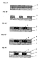
- the Figure is a view showing a process of the formation method of a cavity between metallic wirings according to the present invention.
- a cavity-forming polymer between multilayered wirings used the present invention is a polyamic acid and/or a polyimide obtained from at least one alicyclic tetracarboxylic acid dianhydride represented by the following general formula (1) and at least one alicyclic diamine represented by the following general formula (2).
- General formula (2) H 2 N-R 2 -NH 2
- R 1 represents a tetravalent alicyclic hydrocarbon group having 4-20 carbon atoms.
- the tetravalent alicyclic hydrocarbon group can contain a cyclic ether structure in the molecule.
- R 2 represents a divalent alicyclic hydrocarbon group having 4-20 carbon atoms.
- Examples of the tetravalent alicyclic hydrocarbon group having 4-20 carbon atoms represented by R 1 in the general formula (1) include tetravalent alicyclic hydrocarbon groups represented by the following formulae (3) to (27).
- alicyclic tetracarboxylic acid dianhydride represented by the general formula (1) and containing one of the tetravalent alicyclic hydrocarbon groups represented by the formulae (3) to (27).
- the alicyclic tetracarboxylic acid dianhydride can be used alone or as mixtures of two or more thereof.
- Examples of the divalent alicyclic hydrocarbon group having 4-20 carbon atoms represented by R 2 in the general formula (2) include divalent alicyclic hydrocarbon groups represented by the following formulae (28) to (61).
- the polyamic acid and/or the polyimide that is the cavity-forming polymer between metallic wirings is prepared by the following method.
- At least one aliphatic tetracarboxylic acid dianhydride represented by the general formula (1) and at least one alicyclic diamine represented by the general formula (2) are reacted in an aprotic polar solvent and/or a phenol based solvent in a solids concentration of 1-30 % by weight at a temperature in the range of 0-150°C for 1-24 hours, to obtain a polyamic acid solution.
- a dehydrating agent in an amount of 1-20 moles per mole of the aliphatic tetracarboxylic acid dianhydride represented by the general formula (1) and an imidation catalyst in an amount of 0.5-30 moles per mole of the aliphatic tetracarboxylic acid dianhydride represented by the general formula (1) are added to react the resulting polyamic acid solution at a temperature in the range of 0-180°C for 1-24 hours.
- a polyimide solution is obtained.
- the polyimide that can be used includes polyimides in which the polyamic acid is partially imidated.
- the polyamic acid solution and/or the polyimide solution used in the present invention can be substituted with other organic solvent by the conventional procedure, if desired.
- the aprotic polar solvent used in the present invention is not particularly limited so far as it can dissolve the polyamic acid formed by the reaction therein.
- Preferred examples of the aprotic polar solvent include ⁇ -butyrolactone, cyclohexanone, N-methyl-2- pyrrolidone, N,N-dimethylacetamide, N,N-dimethylformamide, dimethyl sulfoxide, tetramethylurea, and hexamethyl sulfonamide.
- the phenol based solvent used in the present invention is not particularly limited so far as it can dissolve the polyamic acid formed by the reaction therein.
- Preferred examples phenol based include m-cresol, xylenol, phenol, and halogenated phenols.
- the alicyclic tetracarboxylic acid dianhydride represented by the general formula (1) and the alicyclic diamine represented by the general formula (2) while adjusting the use proportion such that the amount of the acid anhydride group in the alicyclic tetracarboxylic acid anhydride is 0.2-2 equivalents, and preferably 0.7-1.3 equivalents, to one equivalent of the amino group in the alicyclic diamine compound.
- the dehydrating agent used in the present invention is not particularly limited so far as it can be dissolved or dispersed in the aprotic polar solvent and/or phenol based solvent.
- Preferred examples include acetic anhydride, propionic anhydride, and trifluoroacetic anhydride.
- the imidation catalyst used in the invention is not particularly limited so far as it is a tertiary amine that can be dissolved or dispersed in the aprotic polar solvent and/or phenol based solvent.
- Preferred examples include aliphatic tertiary amines such as trimethylamine, triethylamine, tripropylamine or tributylamine; aromatic tertiary amines such as N,N-dimethylaniline; and heterocyclic compounds such as pyridine, 2-methylpyridine, N-methylimidazole or quinoline.
- substitution solvent used in the present invention is not particularly limited so far as it is an organic solvent that can dissolve the polyamic acid and/or polyimide therein.
- Preferred examples include the above-described aprotic solvents, the above-described phenol based solvents, and alcohol based solvents such as diacetone alcohol.
- the polyamic acid and/or polyimide synthesized according to the above method preferably has a weight average molecular weight, as reduced into polystyrene measured by gel permeation chromatography, in the range of 1,000-500,000.
- a weight average molecular weight as reduced into polystyrene measured by gel permeation chromatography
- heat resistance of the resulting polymer may be insufficient, or the solution viscosity increases so that handling properties such as coating properties may be lowered, and hence, such is not preferable.
- the alicyclic polymer used in the present invention has a weight loss on heating at 350°C for one hour in an inert gas atmosphere and/or a vacuum atmosphere of 5% by weight or less and a weight loss on heating at 500°C for one hour in an inert gas atmosphere and/or a vacuum atmosphere of 80% by weight or more.
- the heat decomposable alicyclic polymer having a specific heat resistant temperature and a specific heat decomposition temperature can be removed only by simple heat treatment and has a mechanical strength that is sufficiently adaptive to the wiring processing process at temperatures of the heat resistant temperature or lower. Accordingly, it is possible to readily form a cavity structure between metallic wirings in semiconductors, etc., by using the alicyclic polymer of the present invention.
- the inert gas examples include rare gases such as helium, neon, argon, krypton, xenon or radon, and nitrogen.
- the inert gas generally used has a purity of 99.9% or more.
- the inert gas having a purity of 99.99% or more is preferably used, and the inert gas having a purity of 99.999% or more is particularly preferably used.
- Preferable examples of the inert gas used are nitrogen, argon, and helium.
- the vacuum atmosphere is usually 100 Torr or less, preferably 10 Torr or less, and more preferably 1 Torr or less.
- the alicyclic polymer used in the present invention usually has a weight loss on heating at 350°C for one hour in an inert gas atmosphere and/or a vacuum atmosphere of 5% by weight or less, preferably 3% by weight or less, and more preferably 1% by weight or less.
- the alicyclic polymer is thermally stable at a temperature of 350°C or lower at which processing of metallic wirings, etc., of semiconductor devices is usually carried out and therefore, is preferable as a material for formation processing of semiconductor devices.
- the alicyclic polymer usually has a weight loss on heating at 500°C for one hour in an inert gas atmosphere and/or a vacuum atmosphere of 80% by weight or more, preferably 90% by weight or more, and more preferably 95% by weight or more.
- an inert gas atmosphere 80% by weight or more, preferably 90% by weight or more, and more preferably 95% by weight or more.
- hydrogen, oxygen, ammonia, water, etc. it is possible to incorporate hydrogen, oxygen, ammonia, water, etc., in the inert gas atmosphere.
- the amount of the component incorporated is not particularly limited but is usually 50% by volume or less, and preferably 25% by volume or less.
- the alicyclic polymer has good heat decomposition properties at 500°C or lower and can be removed only by a simple heat treatment without necessity of an operation, such as etching or icing, that is usually employed during the formation processing of semiconductor devices. This makes it possible to easily form a cavity structure between metallic wirings in semiconductor devices, etc.
- the alicyclic polymer usually has a glass transition temperature of 200°C or higher, preferably 220°C or higher, and more preferably 240°C or higher. As described above, the alicyclic polymer has a high glass transition temperature, and hence, is preferable from the standpoints that even when exposed to high temperatures during the formation of metallic wirings in the semiconductor device, it does not exhibit a large change in volume following phase transition and keeps stability of the wiring shape.
- the alicyclic polymer has a mechanical strength sufficiently endurable to the formation processing of semiconductors. Specifically, since the alicyclic polymer usually has a hardness of 0.2 GPa or more, preferably 0.3 GPa or more, and more preferably 0.4 GPa or more, and usually has an elastic modulus of 5.0 GPa or more, preferably 6.0 GPa or more, and more preferably 7.0 GPa or more, it can be adapted to the formation processing of semiconductor devices such CMP.
- the alicyclic polymer can be processed into a film shape and provided for the use.
- the film of the alicyclic polymer can be obtained by diluting the polyamic acid and/or polyimide with an organic solvent, etc., forming the solution into a film shape by various processes such as a spin coating process, a dip coating process, a roll coating process, a flow coating process, a spray coating process or a hot press process, and optionally heating at a temperature of the heat decomposition temperature or lower of the alicyclic polymer to remove the unnecessary organic solvent.
- the alicyclic polymer makes it possible to easily form a cavity structure between metallic wirings in semiconductor devices, etc.
- the alicyclic polymer is applied to the surface of a prescribed first dielectric film of a semiconductor substrate (see Fig. 1A).
- the alicyclic polymer is patterned in a space for forming a metallic wiring using the conventional lithography technology and etching technology (see Fig. 1B).
- a metal such as Cu, Al, W or Mo is embedded in the pattern formed on the alicyclic polymer by the conventional method such as plating or CVD (see Fig. 1C).
- a layer of TaN, TiN, etc. may be formed between the alicyclic polymer and the metal.
- the surface can be flattened by CMP.
- a second dielectric film is formed on the alicyclic polymer having the metal embedded therein by the conventional spin process, CVD process or the like (see Fig. ID).
- the alicyclic polymer is removed upon heating, whereby a cavity can be formed between the metallic wirings (see Fig. 1E).
- the removal of the alicyclic polymer can be carried out every layer of the multilayered metallic wirings or by repeating the steps of Fig. 1A to Fig. 1D and then getting together some layers.
- a weight average molecular weight as reduced into polystyrene was measured by the GPC process.
- thermogravity (TG) process Upon heating in a nitrogen atmosphere at an arbitrary temperature for one hour, a change in weight was measured by the thermogravity (TG) process.
- a glass transition temperature was measured by the differential scanning calorimetry (DSC) process.
- the measurement was carried out by the nonaindentation process.
- Tthe reaction product was poured into a large amount of methanol to solidify a polymer, which was then recovered and dried at 80°C overnight.
- the resulting polymer was found to have a weight average molecular weight of 23,000.
- the resulting polymer was dissolved in N,N-dimethylacetamide (DMAc), and the solution was applied to a silicon wafer by the spin coating process.
- the silicon wafer was heat treated at 350°C for 30 minutes to obtain a transparent coating film having a film thickness of about 1 ⁇ m. This coating film was measured with respect to weight loss, glass transition temperature, elastic modulus and hardness according to the above-described methods. The results obtained are shown in the Table below.
- the silicon wafer was heat treated at 350°C for 30 minutes to obtain a transparent coating film having a film thickness of about 1 ⁇ m.
- This coating film was measured with respect to weight loss, glass transition temperature, elastic modulus and hardness according to the above methods. The results obtained are shown in the Table below.
- the reaction product was poured into a large amount of methanol to solidify a polymer, which was then recovered and dried at 80°C overnight.
- the resulting polymer was found to have a weight average molecular weight of 21,000.
- the resulting polymer was dissolved in ⁇ -butyrolactone (GBL), and the solution was applied to a silicon wafer by the spin coating process.
- the silicon wafer was heat treated at 350°C for 30 minutes to obtain a transparent coating film having a film thickness of about 1 ⁇ m. This coating film was measured with respect to weight loss, glass transition temperature, elastic modulus and hardness according to the above methods. The results obtained are shown in the Table below.
- the reaction product was poured into a large amount of methanol to solidify a polymer, which was then recovered and dried at 80°C overnight.
- the resulting polymer was found to have a weight average molecular weight of 19,000.
- the resulting polymer was dissolved in DMAc, and the solution was applied to a silicon wafer by the spin coating process.
- the silicon wafer was heat treated at 350°C for 30 minutes to obtain a transparent coating film having a film thickness of 1 ⁇ m. This coating film was measured with respect to weight loss, glass transition temperature, elastic modulus and hardness according to the above methods. The results obtained are shown in the Table below.
- the reaction product was poured into a large amount of methanol to solidify a polymer, which was then recovered and dried at 80°C overnight.
- the resulting polymer was found to have a weight average molecular weight of 25,000.
- the resulting polymer was dissolved in DMAc, and the solution was applied to a silicon wafer by the spin coating process.
- the silicon wafer was heat treated at 350°C for 30 minutes to obtain a transparent coating film having a film thickness of about 1 ⁇ m. This coating film was measured with respect to weight loss, glass transition temperature, elastic modulus and hardness according to the above methods. The results obtained are shown in the Table below.
- the silicon wafer was heat treated at 350°C for 30 minutes to obtain a transparent coating film having a film thickness of about 1 ⁇ m.
- This coating film was measured with respect to weight loss, glass transition temperature, elastic modulus and hardness according to the above methods. The results obtained are shown in the Table below.
- the silicon wafer was heat treated at 350°C for 30 minutes to obtain a transparent coating film having a film thickness of about 1 ⁇ m.
- This coating film was measured with respect to weight loss, glass transition temperature, elastic modulus and hardness according to the above methods. The results obtained are shown in the Table below.
- the resulting polymer was found to have a weight average molecular weight of 900.
- the resulting polymer solution was concentrated in vacuo so as to have a solids concentration of about 20% by weight and applied to a silicon wafer by the spin coating process.
- the silicon wafer was heat treated at 350°C for 30 minutes to obtain a transparent coating film having a film thickness of about 1 ⁇ m.
- This coating film was measured with respect to weight loss, glass transition temperature, elastic modulus and hardness according to the above methods. The results obtained are shown in the Table below.
- the reaction product was poured into a large amount of methanol to solidify a polymer, which was then recovered and dried at 80°C overnight.
- the resulting polymer was found to have a weight average molecular weight of 23,000.
- the resulting polymer was dissolved in ⁇ -butyrolactone (GBL), and the solution was applied to a silicon wafer by the spin coating process.
- the silicon wafer was heat treated at 350°C for 30 minutes to obtain a transparent coating film having a film thickness of about 1 ⁇ m. This coating film was measured with respect to weight loss, glass transition temperature, elastic modulus and hardness according to the above methods. The results obtained are shown in the Table below.
- the reaction product was poured into a large amount of methanol to solidify a polymer, which was then recovered and dried at 80°C overnight.
- the resulting polymer was found to have a weight average molecular weight of 18,000.
- the resulting polymer was dissolved in DMAc, and the solution was applied to a silicon wafer by the spin coating process.
- the silicon wafer was heat treated at 350°C for 30 minutes to obtain a transparent coating film having a film thickness of 1 ⁇ m. This coating film was measured with respect to weight loss, glass transition temperature, elastic modulus and hardness according to the above methods. The results obtained are shown in the Table below.
- the present invention relates to an alicyclic polymer obtained by reacting a specific alicyclic tetracarboxylic acid dianhydride and a specific alicyclic diamine and to a process of producing the same. Since the alicyclic polymer has a specific heat resistant temperature and a specific heat decomposition temperature, it can be removed only by simple heat treatment and has a mechanical strength that is sufficiently adaptive to the wiring processing process at temperatures of the heat resistant temperature or lower. Accordingly, it is possible to readily form a cavity structure between metallic wirings in semiconductors, etc., by using the alicyclic polymer.
- the method includes a step of coating the surface of a first dielectric film formed on a semiconductor substrate with a polyamic acid and/or a polyimide, a step of patterning a cavity-forming polymer between the multilayered wirings, a step of forming a second dielectric film on the cavity-forming polymer between the multilayered wirings containing a metallic wiring, and a step of removing the cavity-forming polymer between the multilayered wirings by heating to form a cavity between the metallic wirings.
Landscapes
- Macromolecular Compounds Obtained By Forming Nitrogen-Containing Linkages In General (AREA)
- Internal Circuitry In Semiconductor Integrated Circuit Devices (AREA)
- Formation Of Insulating Films (AREA)
Applications Claiming Priority (2)
| Application Number | Priority Date | Filing Date | Title |
|---|---|---|---|
| JP2002314248A JP3775375B2 (ja) | 2002-10-29 | 2002-10-29 | 多層配線間の空洞形成方法 |
| JP2002314248 | 2002-10-29 |
Publications (3)
| Publication Number | Publication Date |
|---|---|
| EP1418618A2 true EP1418618A2 (de) | 2004-05-12 |
| EP1418618A3 EP1418618A3 (de) | 2008-01-23 |
| EP1418618B1 EP1418618B1 (de) | 2009-10-21 |
Family
ID=32105369
Family Applications (1)
| Application Number | Title | Priority Date | Filing Date |
|---|---|---|---|
| EP03024703A Expired - Lifetime EP1418618B1 (de) | 2002-10-29 | 2003-10-28 | Verfahren zur Herstellung von Hohlräumen zwischen mehrlagigen Verdrahtungen |
Country Status (6)
| Country | Link |
|---|---|
| US (1) | US7005248B2 (de) |
| EP (1) | EP1418618B1 (de) |
| JP (1) | JP3775375B2 (de) |
| KR (1) | KR101062556B1 (de) |
| DE (1) | DE60329741D1 (de) |
| TW (1) | TWI248450B (de) |
Cited By (8)
| Publication number | Priority date | Publication date | Assignee | Title |
|---|---|---|---|---|
| EP1930382A4 (de) * | 2005-09-28 | 2010-01-27 | Central Glass Co Ltd | Beschichtungsstoffe aus nieder- oder mittelmolekularen organischen verbindungen |
| US8067527B2 (en) | 2006-07-10 | 2011-11-29 | Nissan Chemical Industries, Ltd. | Polyamic acid and polyimide |
| WO2012097153A1 (en) * | 2011-01-12 | 2012-07-19 | SanDisk Technologies, Inc. | Method of manufacturing air gap isolation in high-density non-volatile memory |
| US8946048B2 (en) | 2010-06-19 | 2015-02-03 | Sandisk Technologies Inc. | Method of fabricating non-volatile memory with flat cell structures and air gap isolation |
| US9123714B2 (en) | 2012-02-16 | 2015-09-01 | Sandisk Technologies Inc. | Metal layer air gap formation |
| US9123577B2 (en) | 2012-12-12 | 2015-09-01 | Sandisk Technologies Inc. | Air gap isolation in non-volatile memory using sacrificial films |
| US9349740B2 (en) | 2014-01-24 | 2016-05-24 | Sandisk Technologies Inc. | Non-volatile storage element with suspended charge storage region |
| US9379120B2 (en) | 2010-06-20 | 2016-06-28 | Sandisk Technologies Inc. | Metal control gate structures and air gap isolation in non-volatile memory |
Families Citing this family (6)
| Publication number | Priority date | Publication date | Assignee | Title |
|---|---|---|---|---|
| JP5040254B2 (ja) * | 2006-10-18 | 2012-10-03 | 東洋紡績株式会社 | ポリイミド系樹脂およびそれを用いたフレキシブル配線板 |
| JP2008243907A (ja) * | 2007-03-26 | 2008-10-09 | Jsr Corp | 導電層間の空洞形成用組成物、導電層間の空洞形成用犠牲膜および導電層間の空洞形成方法 |
| KR20130111154A (ko) * | 2012-03-30 | 2013-10-10 | 주식회사 엘지화학 | 유기전자소자용 기판 |
| JP7390194B2 (ja) * | 2020-01-17 | 2023-12-01 | 東京エレクトロン株式会社 | エアギャップ形成方法 |
| CN112501593B (zh) * | 2020-10-29 | 2022-09-30 | 长芯科技(上海)有限公司 | 一种流量传感器芯片的制造方法 |
| TW202436430A (zh) * | 2023-03-03 | 2024-09-16 | 日商日產化學股份有限公司 | 空洞形成用組成物 |
Family Cites Families (8)
| Publication number | Priority date | Publication date | Assignee | Title |
|---|---|---|---|---|
| US244580A (en) * | 1881-07-19 | Straw rope or band making machine | ||
| US244574A (en) * | 1881-07-19 | Device for postaae | ||
| US5210174A (en) * | 1989-11-22 | 1993-05-11 | Mitsui Toatsu Chemicals, Inc. | Preparation process of polyimide |
| US5461003A (en) * | 1994-05-27 | 1995-10-24 | Texas Instruments Incorporated | Multilevel interconnect structure with air gaps formed between metal leads |
| ATE415704T1 (de) * | 1997-01-21 | 2008-12-15 | Georgia Tech Res Inst | Herstellung eines halbleiterbauelements mit luftspalten für niedrigstkapazitive leiterbahnen |
| US6777159B1 (en) | 1999-05-31 | 2004-08-17 | Pi R&D Co., Ltd. | Method for forming polyimide pattern using photosensitive polyimide and composition for use therein |
| JP2002146021A (ja) | 2000-11-10 | 2002-05-22 | Ube Ind Ltd | 可溶性、透明なポリイミドおよびその製造法 |
| JP2004149607A (ja) * | 2002-10-29 | 2004-05-27 | Jsr Corp | 多層配線間の空洞形成用重合体およびその製造方法 |
-
2002
- 2002-10-29 JP JP2002314248A patent/JP3775375B2/ja not_active Expired - Fee Related
-
2003
- 2003-10-28 DE DE60329741T patent/DE60329741D1/de not_active Expired - Lifetime
- 2003-10-28 US US10/693,972 patent/US7005248B2/en not_active Expired - Lifetime
- 2003-10-28 KR KR1020030075309A patent/KR101062556B1/ko not_active Expired - Fee Related
- 2003-10-28 EP EP03024703A patent/EP1418618B1/de not_active Expired - Lifetime
- 2003-10-29 TW TW092130024A patent/TWI248450B/zh not_active IP Right Cessation
Cited By (12)
| Publication number | Priority date | Publication date | Assignee | Title |
|---|---|---|---|---|
| EP1930382A4 (de) * | 2005-09-28 | 2010-01-27 | Central Glass Co Ltd | Beschichtungsstoffe aus nieder- oder mittelmolekularen organischen verbindungen |
| US7919224B2 (en) | 2005-09-28 | 2011-04-05 | Central Glass Company, Limited | Coating materials consisting of low- or medium-molecular organic compounds |
| US8067527B2 (en) | 2006-07-10 | 2011-11-29 | Nissan Chemical Industries, Ltd. | Polyamic acid and polyimide |
| US8946048B2 (en) | 2010-06-19 | 2015-02-03 | Sandisk Technologies Inc. | Method of fabricating non-volatile memory with flat cell structures and air gap isolation |
| US9698149B2 (en) | 2010-06-19 | 2017-07-04 | Sandisk Technologies Llc | Non-volatile memory with flat cell structures and air gap isolation |
| US9379120B2 (en) | 2010-06-20 | 2016-06-28 | Sandisk Technologies Inc. | Metal control gate structures and air gap isolation in non-volatile memory |
| WO2012097153A1 (en) * | 2011-01-12 | 2012-07-19 | SanDisk Technologies, Inc. | Method of manufacturing air gap isolation in high-density non-volatile memory |
| US8778749B2 (en) | 2011-01-12 | 2014-07-15 | Sandisk Technologies Inc. | Air isolation in high density non-volatile memory |
| US9123714B2 (en) | 2012-02-16 | 2015-09-01 | Sandisk Technologies Inc. | Metal layer air gap formation |
| US9123577B2 (en) | 2012-12-12 | 2015-09-01 | Sandisk Technologies Inc. | Air gap isolation in non-volatile memory using sacrificial films |
| US9349740B2 (en) | 2014-01-24 | 2016-05-24 | Sandisk Technologies Inc. | Non-volatile storage element with suspended charge storage region |
| US9548311B2 (en) | 2014-01-24 | 2017-01-17 | Sandisk Technologies Llc | Non-volatile storage element with suspended charge storage region |
Also Published As
| Publication number | Publication date |
|---|---|
| TWI248450B (en) | 2006-02-01 |
| DE60329741D1 (de) | 2009-12-03 |
| US7005248B2 (en) | 2006-02-28 |
| TW200424235A (en) | 2004-11-16 |
| US20040092127A1 (en) | 2004-05-13 |
| KR20040038723A (ko) | 2004-05-08 |
| JP2004149609A (ja) | 2004-05-27 |
| EP1418618B1 (de) | 2009-10-21 |
| KR101062556B1 (ko) | 2011-09-06 |
| EP1418618A3 (de) | 2008-01-23 |
| JP3775375B2 (ja) | 2006-05-17 |
Similar Documents
| Publication | Publication Date | Title |
|---|---|---|
| EP1418618B1 (de) | Verfahren zur Herstellung von Hohlräumen zwischen mehrlagigen Verdrahtungen | |
| JP4815690B2 (ja) | ポリイミド、ポリイミド前駆体及びこれらの製造方法 | |
| JP2008214412A (ja) | ポリイミドフィルムおよびその製造方法 | |
| JP2020033540A (ja) | シルセスキオキサン含有ポリイミド | |
| US6265753B1 (en) | Interconnect dielectric compositions, preparation thereof, and integrated circuit devices fabricated therewith | |
| US5132386A (en) | Insulating resin composition and semiconductor device using the same | |
| JP3765289B2 (ja) | 多層配線間の空洞形成方法 | |
| JPH06136120A (ja) | 可溶性ポリイミドの製造方法 | |
| JP2561244B2 (ja) | 半導体装置の製造方法 | |
| JP3966743B2 (ja) | 多層感光性樹脂フィルム及びそれからなる絶縁膜 | |
| JPH069222B2 (ja) | 多層配線構造の製造法 | |
| JP4940499B2 (ja) | 低誘電率重合体 | |
| JP4305408B2 (ja) | 絶縁膜用材料、絶縁膜用コーティングワニス、及び、これらを用いた絶縁膜並びに半導体装置 | |
| WO2013111241A1 (ja) | ポリイミド前駆体及びそれを用いた樹脂組成物 | |
| JPH10298285A (ja) | ポリアミック酸およびポリイミド | |
| JP2001323061A (ja) | 低誘電率ポリイミド組成物 | |
| JPS62153313A (ja) | 有機溶媒可溶性ポリイミドおよびその製法 | |
| JP2001217235A (ja) | 半導体素子保護膜形成用感光性樹脂組成物、半導体素子保護用多孔質樹脂および半導体装置 | |
| JP3653888B2 (ja) | ポリアミック酸およびポリイミド | |
| JP2001072769A (ja) | 芳香族ジアミン化合物並びにそれを用いたポリアミド酸及びポリイミド | |
| JP2594545B2 (ja) | 半導体装置の製造方法 | |
| JPS6227432A (ja) | 有機溶媒可溶性ポリイミド | |
| JP2664902B2 (ja) | 半導体装置の製造方法 | |
| JP2000302868A (ja) | 芳香族ジアミン化合物並びにそれを用いたポリアミド酸及びポリイミド | |
| JPH05222195A (ja) | ポリイミド系樹脂前駆体の製造法および樹脂組成物 |
Legal Events
| Date | Code | Title | Description |
|---|---|---|---|
| PUAI | Public reference made under article 153(3) epc to a published international application that has entered the european phase |
Free format text: ORIGINAL CODE: 0009012 |
|
| AK | Designated contracting states |
Kind code of ref document: A2 Designated state(s): AT BE BG CH CY CZ DE DK EE ES FI FR GB GR HU IE IT LI LU MC NL PT RO SE SI SK TR |
|
| AX | Request for extension of the european patent |
Extension state: AL LT LV MK |
|
| PUAL | Search report despatched |
Free format text: ORIGINAL CODE: 0009013 |
|
| AK | Designated contracting states |
Kind code of ref document: A3 Designated state(s): AT BE BG CH CY CZ DE DK EE ES FI FR GB GR HU IE IT LI LU MC NL PT RO SE SI SK TR |
|
| AX | Request for extension of the european patent |
Extension state: AL LT LV MK |
|
| 17P | Request for examination filed |
Effective date: 20080311 |
|
| 17Q | First examination report despatched |
Effective date: 20080410 |
|
| AKX | Designation fees paid |
Designated state(s): BE DE FR GB NL |
|
| GRAP | Despatch of communication of intention to grant a patent |
Free format text: ORIGINAL CODE: EPIDOSNIGR1 |
|
| GRAS | Grant fee paid |
Free format text: ORIGINAL CODE: EPIDOSNIGR3 |
|
| GRAA | (expected) grant |
Free format text: ORIGINAL CODE: 0009210 |
|
| AK | Designated contracting states |
Kind code of ref document: B1 Designated state(s): BE DE FR GB NL |
|
| REG | Reference to a national code |
Ref country code: GB Ref legal event code: FG4D |
|
| REF | Corresponds to: |
Ref document number: 60329741 Country of ref document: DE Date of ref document: 20091203 Kind code of ref document: P |
|
| NLV1 | Nl: lapsed or annulled due to failure to fulfill the requirements of art. 29p and 29m of the patents act | ||
| PG25 | Lapsed in a contracting state [announced via postgrant information from national office to epo] |
Ref country code: BE Free format text: LAPSE BECAUSE OF FAILURE TO SUBMIT A TRANSLATION OF THE DESCRIPTION OR TO PAY THE FEE WITHIN THE PRESCRIBED TIME-LIMIT Effective date: 20091021 |
|
| PLBE | No opposition filed within time limit |
Free format text: ORIGINAL CODE: 0009261 |
|
| STAA | Information on the status of an ep patent application or granted ep patent |
Free format text: STATUS: NO OPPOSITION FILED WITHIN TIME LIMIT |
|
| 26N | No opposition filed |
Effective date: 20100722 |
|
| GBPC | Gb: european patent ceased through non-payment of renewal fee |
Effective date: 20100121 |
|
| PG25 | Lapsed in a contracting state [announced via postgrant information from national office to epo] |
Ref country code: GB Free format text: LAPSE BECAUSE OF NON-PAYMENT OF DUE FEES Effective date: 20100121 |
|
| PG25 | Lapsed in a contracting state [announced via postgrant information from national office to epo] |
Ref country code: NL Free format text: LAPSE BECAUSE OF FAILURE TO SUBMIT A TRANSLATION OF THE DESCRIPTION OR TO PAY THE FEE WITHIN THE PRESCRIBED TIME-LIMIT Effective date: 20091021 |
|
| REG | Reference to a national code |
Ref country code: FR Ref legal event code: PLFP Year of fee payment: 14 |
|
| PGFP | Annual fee paid to national office [announced via postgrant information from national office to epo] |
Ref country code: FR Payment date: 20160919 Year of fee payment: 14 |
|
| PGFP | Annual fee paid to national office [announced via postgrant information from national office to epo] |
Ref country code: DE Payment date: 20161025 Year of fee payment: 14 |
|
| REG | Reference to a national code |
Ref country code: DE Ref legal event code: R119 Ref document number: 60329741 Country of ref document: DE |
|
| REG | Reference to a national code |
Ref country code: FR Ref legal event code: ST Effective date: 20180629 |
|
| PG25 | Lapsed in a contracting state [announced via postgrant information from national office to epo] |
Ref country code: DE Free format text: LAPSE BECAUSE OF NON-PAYMENT OF DUE FEES Effective date: 20180501 |
|
| PG25 | Lapsed in a contracting state [announced via postgrant information from national office to epo] |
Ref country code: FR Free format text: LAPSE BECAUSE OF NON-PAYMENT OF DUE FEES Effective date: 20171031 |