EP1410423B1 - Flash anneal - Google Patents
Flash anneal Download PDFInfo
- Publication number
- EP1410423B1 EP1410423B1 EP02748190A EP02748190A EP1410423B1 EP 1410423 B1 EP1410423 B1 EP 1410423B1 EP 02748190 A EP02748190 A EP 02748190A EP 02748190 A EP02748190 A EP 02748190A EP 1410423 B1 EP1410423 B1 EP 1410423B1
- Authority
- EP
- European Patent Office
- Prior art keywords
- radiation energy
- substrate
- energy source
- wafer
- radiation
- Prior art date
- Legal status (The legal status is an assumption and is not a legal conclusion. Google has not performed a legal analysis and makes no representation as to the accuracy of the status listed.)
- Expired - Lifetime
Links
Images


Classifications
-
- H—ELECTRICITY
- H01—ELECTRIC ELEMENTS
- H01L—SEMICONDUCTOR DEVICES NOT COVERED BY CLASS H10
- H01L21/00—Processes or apparatus adapted for the manufacture or treatment of semiconductor or solid state devices or of parts thereof
- H01L21/02—Manufacture or treatment of semiconductor devices or of parts thereof
- H01L21/04—Manufacture or treatment of semiconductor devices or of parts thereof the devices having potential barriers, e.g. a PN junction, depletion layer or carrier concentration layer
- H01L21/18—Manufacture or treatment of semiconductor devices or of parts thereof the devices having potential barriers, e.g. a PN junction, depletion layer or carrier concentration layer the devices having semiconductor bodies comprising elements of Group IV of the Periodic Table or AIIIBV compounds with or without impurities, e.g. doping materials
- H01L21/30—Treatment of semiconductor bodies using processes or apparatus not provided for in groups H01L21/20 - H01L21/26
- H01L21/324—Thermal treatment for modifying the properties of semiconductor bodies, e.g. annealing, sintering
-
- H—ELECTRICITY
- H01—ELECTRIC ELEMENTS
- H01L—SEMICONDUCTOR DEVICES NOT COVERED BY CLASS H10
- H01L21/00—Processes or apparatus adapted for the manufacture or treatment of semiconductor or solid state devices or of parts thereof
- H01L21/67—Apparatus specially adapted for handling semiconductor or electric solid state devices during manufacture or treatment thereof; Apparatus specially adapted for handling wafers during manufacture or treatment of semiconductor or electric solid state devices or components ; Apparatus not specifically provided for elsewhere
- H01L21/67005—Apparatus not specifically provided for elsewhere
- H01L21/67011—Apparatus for manufacture or treatment
- H01L21/67098—Apparatus for thermal treatment
- H01L21/67115—Apparatus for thermal treatment mainly by radiation
-
- C—CHEMISTRY; METALLURGY
- C30—CRYSTAL GROWTH
- C30B—SINGLE-CRYSTAL GROWTH; UNIDIRECTIONAL SOLIDIFICATION OF EUTECTIC MATERIAL OR UNIDIRECTIONAL DEMIXING OF EUTECTOID MATERIAL; REFINING BY ZONE-MELTING OF MATERIAL; PRODUCTION OF A HOMOGENEOUS POLYCRYSTALLINE MATERIAL WITH DEFINED STRUCTURE; SINGLE CRYSTALS OR HOMOGENEOUS POLYCRYSTALLINE MATERIAL WITH DEFINED STRUCTURE; AFTER-TREATMENT OF SINGLE CRYSTALS OR A HOMOGENEOUS POLYCRYSTALLINE MATERIAL WITH DEFINED STRUCTURE; APPARATUS THEREFOR
- C30B31/00—Diffusion or doping processes for single crystals or homogeneous polycrystalline material with defined structure; Apparatus therefor
- C30B31/06—Diffusion or doping processes for single crystals or homogeneous polycrystalline material with defined structure; Apparatus therefor by contacting with diffusion material in the gaseous state
- C30B31/12—Heating of the reaction chamber
-
- H—ELECTRICITY
- H05—ELECTRIC TECHNIQUES NOT OTHERWISE PROVIDED FOR
- H05B—ELECTRIC HEATING; ELECTRIC LIGHT SOURCES NOT OTHERWISE PROVIDED FOR; CIRCUIT ARRANGEMENTS FOR ELECTRIC LIGHT SOURCES, IN GENERAL
- H05B3/00—Ohmic-resistance heating
- H05B3/0033—Heating devices using lamps
- H05B3/0038—Heating devices using lamps for industrial applications
- H05B3/0047—Heating devices using lamps for industrial applications for semiconductor manufacture
Definitions
- This invention generally relates to semiconductor manufacturing equipment and, more particularly, to a system and method for rapid thermal processing of a semiconductor wafer.
- Rapid Thermal Processing typically includes quickly raising the temperature of the wafer and holding it at that temperature for a time long enough to successfully perform a fabrication process, while avoiding such problems as unwanted dopant diffusion that would otherwise occur at the high processing temperatures.
- the light source is usually a bank of Halogen lamps that emit radiation energy that is focused on the wafer by the reflectors.
- Halogen lamp-based RTP systems have considerable drawbacks with regard to achieving and maintaining a uniform temperature distribution across the active layer of the wafer surface.
- the Halogen lamp has a filament, which generates broadband radiation. By applying more power to the filament, the intensity of the lamp can be increased.
- silicon wafers are heated using a useable band of short wavelengths, and are otherwise transparent to wavelengths outside of this band. The radiation from the lamp remains mostly outside of the useable wavelength band during typical halogen lamp operation. As a consequence, much of the applied power is wasted.
- filament type lamps are generally create a broad wavelength distribution that is independently uncontrollable. Consequently, temperature fluctuations occur on the surface of the wafer which may cause crystal defects and slip dislocations in the wafer at high temperatures (e.g. ⁇ 1000°C) and under various lamp configurations.
- a film must be used that does not degrade over time, and must not sputter, bubble, or degas when heated, otherwise non-uniform absorption will result. Because of the requirements placed on the thin absorption film, the materials for this film are limited. As a result, the same RTP apparatus may heat wafers differently and unpredictably, which wastes both time and materials.
- US-A-6 080 965 discloses a system for thermal processing comprising a radiation source which emits light that is reflected from a mirror and onto a window through a transparent window.
- US-A-5 893 952 relates to an apparatus for rapid thermal processing of a substrate with a high-wattage laser as an energy source and transmitted to an optical scanner via an optical switch for scanning across the surface of the wafer.
- US-A-5 446 825 discloses an apparatus for rapid thermal processing with multiple lamps and a reflector for directing light from the lamps through an optical quartz window and onto the surface of the wafer.
- the present invention provides a system and method for uniformly and controllably heating the active surface of a semiconductor wafer or substrate during processing.
- the present invention may include, as described in greater detail below, a radiation energy source provided, which is enclosed or substantially surrounded by a reflective/absorptive surface, which both reflects and absorbs the radiation, emitted from the energy source such that the resultant energy output as seen by the wafer is substantially free of non-uniformity.
- the resultant energy can be uniformly spread over the wafer to heat only the active layer of the wafer surface. Because the resultant energy is uniform over the diameter of the wafer there is no significant heating overlap.
- the resultant energy can be provided at a very high intensity such that only a short exposure time is necessary to heat the active layer of the substrate.
- the process can be referred to as a "flash" anneal process, which can include crystallizing the active layer of the substrate, doping the active layer, or otherwise heat treating the active layer.
- the present invention can provide a continuous heat exposure to allow the bulk of the substrate to be heated.
- a system for rapid thermal processing of a substrate.
- the system includes a radiation energy source surrounded by a reflector, and a radiation outlet channel which concentrates the radiation energy.
- the outlet allows at least a portion of the concentrated radiation energy to escape from the surrounding reflector, which causes radiation energy to impinge on a surface of a substrate to heat an active layer of the substrate.
- the surface of the substrate is impinged on by the radiation energy for a substantially instantaneous reaction time.
- the radiation energy source comprises a plurality of high-intensity lamps.
- the substrate is preferably housed in a non-oxygenated environment.
- the reflector includes a reflective surface for focusing the radiation energy from the radiation energy source at a first focal point.
- the radiation energy is focused to impinge on the surface of a substrate for a time of between about 1 nanosecond and about 10 seconds. This raises the temperature of the active layer of the substrate in a substantially instantaneous time to between about 500°C and about 1400°C.
- an energy flux emanating from the first focal point impinges on the surface of the substrate.
- the radiation energy source is preferably an Xe arc lamp.
- a method for rapid thermal processing of a substrate.
- the method includes providing a chamber including a radiation energy source, a reflector enclosing the energy source and an outlet channel.
- the outlet channel concentrates the radiation energy through a slit, and flashes the radiation energy source to impinge on a surface of a substrate to heat an active layer of the substrate.
- the temperature of the active layer is between about 500°C and 1400°C, and the flashing time is between about 1 nanosecond and about 10 seconds.
- the inner surface of the reflector is preferably coated with a material taken from the group consisting of gold and silver, and preferably reflects wavelengths of less than about 900 nm.
- an alternative method for rapid thermal processing of a substrate.
- the method includes providing a chamber including a radiation energy source, a reflector enclosing the energy source and an outlet channel.
- the outlet channel concentrates the radiation energy though a slit.
- the radiation energy power level is raised to a peak power level to expose an active layer of a substrate to a first radiation energy for a substantially instantaneous time duration.
- the first time duration being between about I nanosecond and about 10 seconds and the second time duration being between about zero seconds and about 3600 seconds.
- the radiation energy source includes a high-energy lamp, and has an energy density of between about 0.5 J/cm 2 and about 100 J/cm 2 .
- the active layer of the substrate is preferably between 0.05 ⁇ m and about 1 mm below a surface of said substrate, where the lamp is preferably either includes a flow tube including a cooling fluid, or an Xe arc lamp.
- the system and method of the present invention can be used to heat only the active layer of the substrate surface, thus the process is advantageous for implant anneal applications, such as shallow junction, ultra shallow junction, and source drain anneal.
- flash includes its ordinary meaning as generally understood by those of ordinary skill in the art. This definition includes the definition that flash means to give off light suddenly or substantially instantaneous (or in transient bursts) for a duration of time between about 1 nanosecond and about 10 seconds.
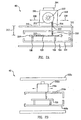
- FIGS 1A and 1B are schematic illustrations of a side view and top view, respectively, of one embodiment of a semiconductor wafer processing system 10 that establishes a representative environment of the present invention.
- Processing system 10 includes a loading station 12 which has multiple platforms 14 for supporting and moving a wafer cassette 16 up and into a loadlock 18.
- Wafer cassette 16 may be a removable cassette which is loaded into a platform 14, either manually or with automated guided vehicles (AGV).
- AGV automated guided vehicles
- Wafer cassette 16 may also be a fixed cassette, in which case wafers are loaded onto cassette 16 using conventional atmospheric robots or loaders (not shown).
- a robot 22 within transfer chamber 20 rotates toward loadlock 18 and picks up a wafer 24 from cassette 16.
- a reactor or thermal processing chamber 26 which may also be at atmospheric pressure or under vacuum, accepts wafer 24 from robot 22 through a gate valve 30.
- additional reactors may be added to the system, for example reactor 28.
- Robot 22 then retracts and, subsequently, gate valve 30 closes to begin the processing of wafer 24.
- gate valve 30 opens to allow robot 22 to pick-up and place wafer 24 into a cooling station 60. Cooling station 60 allows the newly processed wafers, which may have temperatures upwards of 100 °C, to cool before they are placed back into a wafer cassette in loadlock 18.
- reactors 26 and 28 are RTP reactors, such as those used in thermal anneals, dopant diffusion, thermal oxidation, nitridation, chemical vapor deposition, and similar processes.
- Reactors 26 and 28 are generally horizontally displaced, however in a preferred embodiment, reactors 26 and 28 are vertically displaced; ( i.e. stacked one over another) to minimize floor space occupied by system 10.
- Reactors 26 and 28 are bolted onto transfer chamber 20 and are further supported by a support frame 32. Process gases, coolant, and electrical connections may be provided through the rear face of the reactors using interfaces 34.
- FIG. 2A is a simplified illustration of an embodiment of RTP reactor system 40 in accordance with the principles of the present invention.
- reactor system 40 includes a process chamber 102 and a scanner assembly 200.
- Scanner assembly 200 may be positioned proximate to process chamber 102, such that in operation, the scanner assembly can be made to adequately scan the wafer disposed in the chamber.
- process chamber 102 may include a closed-end tube 103, defining an interior cavity 104.
- wafer support posts 106 typically three (of which two are shown), to support a single wafer 108.
- An opening or aperture (not shown) on one end of tube 103 provides access for the loading and unloading of wafer 108 before and after processing.
- the aperture may be a relatively small opening, but large enough to accommodate a wafer of between about 0.5 to 0.8 mm thick and up to 300 mm ( ⁇ 12 in.) in diameter, and the arm and end effector of robot 22.
- the aperture is no greater than between about 18 mm and 22 mm, preferably 20 mm.
- the relatively small aperture size helps to reduce radiation heat loss from tube 103.
- tube 103 requires no internal moving parts to position wafer 108, such as lift pins, actuators, and the like.
- tube 103 may be constructed with a minimal internal volume-surrounding wafer 108.
- the volume of interior cavity 104 is usually no greater than about 1.0 m 3 , and preferably the volume is no greater than about 0.3 m 3 . Accordingly, the small tube volume allows reactor system 40 to be made smaller, and as a result, system 10 may be made smaller, requiring less floor space.
- tube 103 is made of a transparent quartz or similar material.
- FIG. 2A also illustrates scanner assembly 200, which may be used in conjunction with a radiation energy source 202, to provide rapid thermal processing of semiconductor wafer 108.
- Scanner assembly 200 includes a housing 216 which supports an actuator 204, a reflecting chamber 212, and a radiation outlet channel 214.
- the external dimensions of housing 216 are determined by the application. For example, the length of housing 216 may be at least as great, or greater than the diameter of wafer 108.
- Actuator 204 provides a conventional means for making scanner assembly 200 operable to scan wafer 108.
- Actuator 204 may be configured to provide a back and forth scanning motion, as indicated in FIG. 2A by arrows 206 and 208, along a scanning length of tube 103.
- Actuator 204 may include, but is not limited to, conventional drivers and motion translation mechanisms, such as linear motors, stepper motors, hydraulic drives, and the like, and gears, pulleys, chains, and the like.
- scanner assembly 200 may be mounted external to both process chamber 102 and tube 103.
- Scanner assembly 200 is positioned above an optical window 210, which is provided along the scanning length of chamber 102 (i.e. at least as great as the diameter of wafer 108) to allow the radiation energy emitted from housing 216 to enter tube 103 and impinge on wafer 108.
- the scanning motion of scanner assembly 200a may take place internal to process chamber 102a, but external to tube 103a.
- Scanner assembly 200a is positioned above optical window 210a, formed on tube 103a along the scanning length (i.e. at least as great as the diameter of wafer 108) to allow the radiation energy emitted from housing 216a to enter tube 103a and impinge on wafer 108.
- scanner assembly 200b may be mounted external to process chamber 102b, with no process tube.
- scanner assembly 200b is positioned above optical window 210b, which is provided along the scanning length of chamber 102b (i.e. at least as great as the diameter of wafer 108) to allow the radiation energy emitted from housing 216b to impinge on wafer 108.
- Optical window 210 may be made of any material that allows for the transmission of the radiation energy, preferably quartz.
- Window 210 may have a thickness of between about 1 mm and about 5 mm and a diameter that is at least as great or greater than wafer 108.
- the distance between the surface of the wafer and the scanner assembly, indicated in FIG. 2A as gap 213, should be no greater than about 50 mm, preferably between about 10 mm and 25 mm.
- the relatively small gap 213 ensures that adequate control of the temperature/radiation energy distribution across wafer 108 is maintainable. A larger gap 213 may cause some of the radiation energy to escape before it impinges on wafer 108.
- Radiation source 202 is disposed within reflective chamber 212, typically positioned such that substantially all of the broadband radiation is allowed to impinge on an internal surface 218 of the chamber.
- radiation energy source 202 may be a high-intensity lamp of the type conventionally used in lamp heating operations.
- radiation energy source 202 is a filament-less lamp, such as a Xe arc lamp. Typical, power requirements for the preferred lamp 202 of the present invention are between about 500 Watts and about 50 kWatts.
- surface 218 of chamber 212 which is highly reflective of certain wavelengths and absorptive or non-reflective of others.
- surface 218 is coated with a material, which has the reflecting/absorbing characteristic.
- surface 218 may be coated with gold or silver, where the silver is further coated with a protection coating, such as SiN or any transparent coating, which prohibits oxidation of the silver.
- the coating efficiently reflects wavelengths of less than 900 nm, to produce an average wavelength of between about 900 nm and about 200 nm.
- Chamber 212 which may be formed into any suitable geometric shape.
- chamber 212 may be a round chamber.
- light energy can be focused at the center of chamber 212 and directed toward radiation outlet channel 214, described below.
- radiation energy source 202 can be off-center in chamber 212 to ensure that the focused light energy does not over heat energy source 202.
- FIG. 3 shows an alternative example of chamber 212, which may be formed into an elliptical chamber.
- Elliptical chamber 212 can have two focal points.
- Energy source 202 can be positioned at a first focal point 203, such that the light energy is focused at the second focal point 205 and directed to radiation outlet channel 214.
- Radiation outlet channel 214 can be about 5 mm to 20 mm long; preferably about 10 mm long, to adequately direct the radiation energy along the desired path.
- Radiation outlet channel 214 has an opening or slit 222 formed on the end of the channel which allows a beam 220 of the radiation energy to escape housing 216.
- Slit 222 is designed to shape beam 220 as desired, such that an optimal amount of energy may be focused on wafer 108.
- slit 222 may be a rectangular opening, which extends the length of scanner assembly 200, and is as great, or greater than the diameter of wafer 108.
- slit 222 may have a width of between about 1 mm and 10 mm; preferably 2 mm. As beam 222 is scanned over wafer 108, a uniform temperature distribution is created across the surface of wafer 108, which heats an active layer 224 of the wafer.
- active layer or device layer 224 is a portion of wafer 108, which extends from surface 223 of wafer 108 down to a depth ⁇ below surface 223.
- the depth a is typically between about 0.05 ⁇ m and 1 mm, but will vary with the process and device feature size.
- Active layer 224 is well known in the semiconductor manufacturing industry as that portion of the wafer in which semiconductor devices are formed, such as transistors, diodes, resistors, and capacitors.
- the temperature to which active layer 224 is heated is a function of the relationship between the speed at which scanner assembly 200 is moved across wafer 108 and the power supplied to lamp 202.
- the temperature of active layer 224 may range from between about 500 °C to about 1200 °C.
- the scan rate may vary between about 1 mm/sec to about 100 mm/sec at 500 watts to 50 kwatts. The slower the scan rate, the less power is required.
- wafer 108 can be pre-heated, for example, to about 300° C, such that the processing of active layer 224 begins at the higher temperature, which reduces processing time and saves energy.
- Heating active layer 224 using reactor system 40 increases the diffusion rate and solubility of active layer 224.
- a shallow doped region may be created in active layer 224.
- Doping the active layer includes scanning active layer 224 to a process temperature, for example, from between about 500 °C to about 1200 °C, in an environment of a doping compound, such as boron, phosphorus, nitrogen, arsenic, B 2 H 6 , PH 3 , N 2 O, NO, AsH 3 , and NH 3 .
- the concentration of the compound may range from about 0.1% to about 100% relative to a carrier gas, such as H 2 , N 2 and O 2 or a non-reactive gas, such as argon or helium. Higher concentrations of the compound can speed up the doping process and/or increase the dopant concentration within the active layer.
- FIG. 4 is a simplified illustration of a scanner assembly 300 that includes a high intensity pulse or continuous wave laser 302 to provide rapid thermal processing of semiconductor wafer 304.
- Scanner assembly 300 also includes a laser energy focusing assembly 306 and an actuator 308.
- the components of scanning assembly 300 may be enclosed in a single housing, which is mountable on to a process chamber 320 in a manner similar to the embodiments described above in FIG. 2A.
- Laser focusing assembly 306 includes a first focusing lens 310, a second focusing lens 312, and mirror 314. Focusing assembly operates in a well-known, conventional manner to focus the laser energy 301 from laser 302 onto wafer 304.
- the laser energy 301 from laser 302 can have a wavelength of less than 1 ⁇ m.
- Actuator 308 provides a conventional means for making scanner assembly 300 operable to scan wafer 304.
- Actuator 308 may be configured to move laser 302 and focusing assembly 306 to provide a back and forth scanning motion across wafer 304, as indicated in FIG. 4 by arrow 316.
- only mirror 314 may be moved to cause the laser scanning of wafer 304.
- wafer 304 may be made to move, such that a stationary beam 301 can be made to scan the wafer surface.
- Actuator 308 may include, but is not limited to, conventional drivers and motion translation mechanisms, such as linear motors, stepper motors, hydraulic drives, and the like, and gears, pulleys, chains, and the like.
- scanner assembly 300 is positioned above an optical window 318, which is provided along the scanning length of process chamber 320 to allow the laser energy to enter process chamber 320 and impinge on wafer 304.
- Window 318 may be made of any material that allows for the transmission of laser energy 301; preferably transparent quartz.
- Window 318 may have a thickness of between about 1 and about 5 mm and a diameter that is at least as great or greater than wafer 304.
- FIG. 5A is a simplified illustration of an RTP reactor system 500.
- Reactor system 500 includes a process chamber 502 and a reflector assembly 504.
- Reflector assembly 504 may include a reflector 506 and a radiation energy source 508.
- Reflector assembly 504 may be positioned within process chamber 502 proximate to a wafer 510, such that in operation, reflector assembly 504 can be made to adequately process wafer 510.
- Radiation energy source 508 can be a high-intensity lamp of the type conventionally used in lamp heating operations.
- radiation energy source 508 is a filament-less lamp, such as a Xe arc lamp (hereinafter "lamp 508").
- Lamp 508 can be any suitably shaped lamp, for example, a tube shaped lamp that has a length at least as long as the diameter of wafer 510.
- Lamp 508 can be surrounded by a flow tube 512.
- Flow tube 512 can contain a cooling fluid 522, for example, deionized water. Cooling fluid 522 is used to keep lamp 508 from overheating during operation. For example, cooling fluid can keep the temperature of lamp 508 under 100° C to keep any quartz components of lamp 508 from melting.
- cooling fluid 522 can be mixed with a non-conductive die. The non-conductive die can act as a niter to Keep only certain wavelengths from emanating from lamp 508 through flow tube 512.
- FIG. 5B is a simplified illustration of a plurality of lamps 508 disposed proximate to reflector 506. It should be understood that any number of lamps 508 can be used to achieve the desired heating levels required of a specific process.
- Reflector assembly 504 is in operational arrangement with wafer 510.
- Reflector 506 includes an inner surface 514, which can be highly reflective of certain wavelengths and absorptive or non-reflective of others.
- inner surface 514 can be coated with a material, which has the reflecting/absorbing characteristic.
- inner surface 514 may be coated with gold or silver, where the silver is further coated with a protection coating, such as SiN or any transparent coating, which prohibits oxidation of the silver.
- the coating efficiently reflects wavelengths of less than 900 nm, to produce an average wavelength of between about 900 nm and about 200 nm.
- inner surface is highly reflective across the full spectra of ultra violet (UV), infrared (IR) and visible wavelengths.
- Reflector 506 may be formed into any suitable geometric shape.
- reflector 506 may be flat, spherical, elliptical or parabolic.
- the light energy from lamp 508 can be focused at the center or focal point of reflector 506 to be directed toward wafer 510.
- the radiation emitted from lamp 508 and reflected from inner surface 514 of reflector 506 impinges on wafer 510, as simply and representatively illustrated by rays 516, 518 and 520, to provide a uniform temperature distribution across the surface of wafer 510, which heats the active layer 224 of the wafer (as described above in reference to FIG. 2D).
- the temperature to which active layer 224 is heated is a function of the relationship between the power supplied to lamp 508 and the length of time which the radiation energy is allowed to impinge on wafer 510.
- the temperature of active layer 224 may be raised to a range from between about 500 °C to about 1400 °C.
- wafer 510 may be exposed to a flash of lamp 508, where lamp 508 gives off light energy suddenly or substantially instantaneously, for example, for a duration of time between about 1 nanosecond and about 10 seconds at a power level of between about 0.5 J/cm 2 and about 100 J/cm 2 .
- the lamp power can be maintained at a second power level, for example, between about 1000 watts to about 500 kwatts.
- Wafer 510 can be exposed to the second power level for any time duration that may be necessary to complete the processing of wafer 510.
- the continuous exposure can last from between about 0.05 seconds and about 3600 seconds. The continuos exposure can heat the bulk of wafer 510 in addition to heating the active layer during the flash anneal.
- Wafer 510 can be pre-heated, for example, to about 300° C, such that the processing of active layer 224 begins at the higher temperature, which reduces processing time and saves energy.
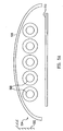
- FIG. 6 is a simplified illustration of a reflector assembly 504.
- Reflector 506 may be formed into an ellipse, which has two focal points F 1 and F 2 .
- Lamp 508 can be positioned at focal point F 1 , such that the energy is reflected from inner surface 514, exemplified by rays 524 and 525, and focused at the second focal point F 2 .
- Wafer 510 can be positioned at focal point F 2 , such that the energy can be used to process wafer 510.
- actuator 526 can be used to provide a conventional means for causing reflector assembly 504 to scan over wafer 510.
- Actuator 526 may be configured to move either wafer 510 or reflector assembly 504 to provide a back and forth scanning motion, as indicated by arrow 528, across wafer 510.
- FIG. 7 is a simplified illustration of reflector assembly 504.
- reflector 506 is formed into an ellipse, with two focal points F 1 and F 2 .
- Lamp 508 is positioned at focal point F 1 , such that the energy is reflected from inner surface 514 and focused at focal point F 2 .
- Wafer 510 is set back a distance d 1 from reflector assembly 504 and/or a distance d 2 from focal point F 2 .
- Distances d 1 and d 2 are selected such that wafer 510 is fully engulfed within a beam 533 emanating from focal point F 2 .
- Beam 533 outlined by rays 530 and 532, covers the entire surface area of wafer 510, such that the entire surface of wafer 510 is subjected simultaneously to substantially all of the reflected energy from lamp 508 to process wafer 510.
- FIG. 8 is an illustration of a reflector assembly 504.
- process chamber 502 including reflector assembly 504 may be mounted external to a second process chamber 536.
- Reflector assembly 504 can be positioned above an optical window 538, which is provided between chambers 502 and 536 to allow the radiation energy emitted from lamp 508 to enter second process chamber 536 and impinge on wafer 510.
- Optical window 538 may be made of any material that allows for the transmission of the radiation energy, preferably quartz.
- Window 538 may have a thickness of between about 1 and about 5 mm and a diameter that is at least as great or greater than wafer 510.
- Second process chamber 536 can be pulled to vacuum, for example, using a pump 540. Second chamber 536 can also be filled through inlet 542 with a non-oxygen gas, such as N 2 . During the processing of wafer 510, the vacuum or non-oxygen environment ensures that the transmission of ultra-violet (UV) wavelengths from lamp 508 can reach wafer 510.
- a non-oxygen gas such as N 2 .
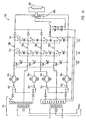
- FIGS. 9A-9D are simplified circuit diagrams of a power supply 600 for a lamp 602 in accordance with an embodiment of the present invention.
- power supply 600 includes a main circuit 604 and an ignition circuit 606.
- main circuit 604 includes an ignition transformer 608 whose primary winding 610 can be supplied with a voltage V 1 , and whose secondary winding 612 ignites lamp 602 with the stepped-up value of voltage V 1 .
- a capacitor 614 is provided in parallel to a series connection of primary winding 610 and a controllable switch 618.
- Capacitor 614 can be of any desired capacitance, for example, between about 10 ⁇ F and 100 F.
- Switch 618 can be, for example, any suitable manual switch, electromagnetic relay or solid state device.
- capacitor 614 can be connected in parallel with a resistor 616 and a diode 620 provided in series with resistor 616.
- resistor 616 acts as a current limiter and/or a dummy load.
- Capacitor 614 is charged when supply voltage V 1 is activated across nodes N 1 and N 2 .
- Voltage V 1 can be an AC voltage supplied via a direct line or a transformer output.
- Voltage V 1 can be adjustable and may range from between about 200 VAC and 1000 VAC.
- Ignition circuit 606 supplies the ignition energy with the aid of a pulse switch 622.
- ignition circuit 606 is provided with secondary winding 612 of ignition transformer 608.
- a resistor 624 in series with diode 626, is provided in series with secondary winding 612 and pulse switch 622.
- a capacitor 628 disposed in parallel to a shunt resistor 630, is in series connection to secondary winding 612.
- Capacitor 628 can be of any desired capacitance, for example, between about 0.5 ⁇ F and 100 ⁇ F.
- Capacitor 628 can be charged by a voltage V 2 , placed across nodes N 3 and N 4 .
- Voltage V 2 can be an AC voltage supplied via a direct line or a transformer output.
- Voltage V 2 can be adjustable and may range from between about 500 VAC and 1000 VAC.
- nodes N 1 and N 2 can be electrically coupled to nodes N 3 and N 4 so as to share the same power source.
- FIG. 9B shows an embodiment of primary circuit 604 and ignition circuit 606 where switches 618 and 619 are closed to allow supply voltage V 1 to be applied between nodes N 1 and N 2 , to begin the charging via resistor 616 of capacitor 614. At the same time, capacitor 628 of ignition circuit 606 is charged via resistor 624 with voltage V 2 applied between nodes N 3 and N 4 .
- FIG. 9C shows an embodiment, such that when capacitor 614 is charged to a desired capacity, switch 618 can be opened and switch 619 can be opened, thus removing the effect of supply voltage V 1 on capacitor 614 and allowing a voltage V c to be supplied from capacitor 614 across primary windings 610.
- Impulse switch 622 can be closed to allow capacitor 628 to discharge, such that a voltage V t is supplied across secondary windings 612. According to the transmission ratio of ignition transformer 608, a current flux generates a stepped-up voltage in primary windings 610 that is high enough to energize lamp 602.
- switch 622 can be released ( i.e. opened) and switch 619 can be closed to allow capacitor 614 to continue to discharge via the dummy load supplied through resistor 616.
- capacitor 628 of ignition circuit 606 begins to be re-charged once switch 622 is opened.
- Primary circuit 604 can be re-charged with the closing of switch 618.
- FIG. 10 is an embodiment of a power supply circuit 700 configured using the principles described in reference to FIGS. 9A-9D.
- This embodiment illustrates the versatility of power supply circuit 700.
- capacitors 708 from a plurality of primary circuits 706 can be stacked together to be used in conjunction with one another to increase the charge storing capacity of power supply 700.
- the stacked capacitors 708 form a first rack 709.
- Each primary circuit 706 can be connected together upon the closing of switches or relays 707.
- a plurality of capacitor racks, such as second rack 711 and third rack 713 can be connected in parallel with first rack 709 via a set of switches 714.
- the racks 709, 711, and 713 can be used together to vary the capacitance and thus the power level supplied to lamp 602.
- FIG. 10 illustrates additional versatility of power supply 700.
- AC power source 702 can be configured to provide a variable voltage, ranging for example between about 200 VAC and about 1000 VAC.
- resistor 704 of the primary circuit can be a halogen lamp or similar device, which can be used to dissipate heat energy and also provide a visual indication that the capacitor in the circuit is being charged or discharged.
- FIG. 11 is an embodiment of a power supply circuit 800 using the principles described in reference to FIGS. 9A-9D with the additional ability to allow a continuous powering of lamp 602. Accordingly, power supply circuit 800 can provide a flash exposure to the radiation energy of lamp 602 followed by a continuous component of exposure to the radiation energy of lamp 602.
- Power supply circuit 800 includes power circuit 802, where switches 804 and 806 when closed allow an AC supply voltage V 1 to be applied between nodes N 1 and N 2 , to begin the charging via resistor 808 of capacitor 810. At the same time, capacitor 812 of ignition circuit 814 is charged via resistor 816.
- a set of diodes 818 are provided to convert the AC voltage supply to a DC voltage supply.
- switch 820 When capacitors 810 and 812 are charged to desired capacities, switch 820 is closed allowing a voltage V 2 to be supplied from capacitor 810 across primary windings 822.
- Impulse switch 824 can be closed to allow capacitor 812 to discharge, such that a voltage V 3 is supplied across secondary windings 826.
- a current flux generates a stepped-up voltage in primary windings 822 that is high enough to energize lamp 602.
- voltage V 2 remains across the primary windings to allow lamp 602 to remain energized and, thus producing a radiation energy output. In this manner, discharge time can be controlled.
- the present invention overcomes many of the disadvantages of RTP systems using Halogen lamps for heating.
- filament-type Halogen lamps produce broadband energy, much of which cannot be used to heat the active layer of the wafer.
- power to the lamp is increased.
- This increase in power shifts the peak intensity.
- the arc lamp used in the present invention does not shift peak intensity with an increase in power and thus can be made to perform at a peak intensity that is within the useable band of wavelengths. As a consequence, the added power is more efficiently consumed at the active layer.
Landscapes
- Engineering & Computer Science (AREA)
- Manufacturing & Machinery (AREA)
- Chemical & Material Sciences (AREA)
- Physics & Mathematics (AREA)
- Power Engineering (AREA)
- Microelectronics & Electronic Packaging (AREA)
- Computer Hardware Design (AREA)
- General Physics & Mathematics (AREA)
- Condensed Matter Physics & Semiconductors (AREA)
- Metallurgy (AREA)
- Toxicology (AREA)
- Health & Medical Sciences (AREA)
- Organic Chemistry (AREA)
- Materials Engineering (AREA)
- Crystallography & Structural Chemistry (AREA)
- Recrystallisation Techniques (AREA)
- Physical Vapour Deposition (AREA)
- Chemical Vapour Deposition (AREA)
- Control Of Resistance Heating (AREA)
- Crystals, And After-Treatments Of Crystals (AREA)
- Glass Compositions (AREA)
Applications Claiming Priority (3)
| Application Number | Priority Date | Filing Date | Title |
|---|---|---|---|
| US910298 | 2001-07-20 | ||
| US09/910,298 US6376806B2 (en) | 2000-05-09 | 2001-07-20 | Flash anneal |
| PCT/US2002/022716 WO2003009350A2 (en) | 2001-07-20 | 2002-07-18 | Flash anneal |
Publications (2)
| Publication Number | Publication Date |
|---|---|
| EP1410423A2 EP1410423A2 (en) | 2004-04-21 |
| EP1410423B1 true EP1410423B1 (en) | 2007-03-07 |
Family
ID=25428586
Family Applications (1)
| Application Number | Title | Priority Date | Filing Date |
|---|---|---|---|
| EP02748190A Expired - Lifetime EP1410423B1 (en) | 2001-07-20 | 2002-07-18 | Flash anneal |
Country Status (8)
| Country | Link |
|---|---|
| US (1) | US6376806B2 (enExample) |
| EP (1) | EP1410423B1 (enExample) |
| JP (2) | JP2004536457A (enExample) |
| KR (1) | KR100809240B1 (enExample) |
| AT (1) | ATE356430T1 (enExample) |
| DE (1) | DE60218690T2 (enExample) |
| TW (1) | TWI270104B (enExample) |
| WO (1) | WO2003009350A2 (enExample) |
Families Citing this family (63)
| Publication number | Priority date | Publication date | Assignee | Title |
|---|---|---|---|---|
| US6048411A (en) * | 1997-05-12 | 2000-04-11 | Silicon Genesis Corporation | Silicon-on-silicon hybrid wafer assembly |
| US20070122997A1 (en) * | 1998-02-19 | 2007-05-31 | Silicon Genesis Corporation | Controlled process and resulting device |
| US6594446B2 (en) * | 2000-12-04 | 2003-07-15 | Vortek Industries Ltd. | Heat-treating methods and systems |
| JP3798674B2 (ja) * | 2001-10-29 | 2006-07-19 | 大日本スクリーン製造株式会社 | 熱処理装置および熱処理方法 |
| US7255899B2 (en) * | 2001-11-12 | 2007-08-14 | Dainippon Screen Mfg. Co., Ltd. | Heat treatment apparatus and heat treatment method of substrate |
| CN101324470B (zh) * | 2001-12-26 | 2011-03-30 | 加拿大马特森技术有限公司 | 测量温度和热处理的方法及系统 |
| US6849831B2 (en) | 2002-03-29 | 2005-02-01 | Mattson Technology, Inc. | Pulsed processing semiconductor heating methods using combinations of heating sources |
| US7005601B2 (en) | 2002-04-18 | 2006-02-28 | Applied Materials, Inc. | Thermal flux processing by scanning |
| US6987240B2 (en) * | 2002-04-18 | 2006-01-17 | Applied Materials, Inc. | Thermal flux processing by scanning |
| JP4429609B2 (ja) * | 2002-06-25 | 2010-03-10 | 大日本スクリーン製造株式会社 | 熱処理装置 |
| US6809035B2 (en) * | 2002-08-02 | 2004-10-26 | Wafermasters, Inc. | Hot plate annealing |
| JP2004134674A (ja) * | 2002-10-11 | 2004-04-30 | Toshiba Corp | 基板処理方法、加熱処理装置、パターン形成方法 |
| US6835914B2 (en) * | 2002-11-05 | 2004-12-28 | Mattson Technology, Inc. | Apparatus and method for reducing stray light in substrate processing chambers |
| US6881681B2 (en) * | 2002-11-22 | 2005-04-19 | Freescale Semiconductor, Inc. | Film deposition on a semiconductor wafer |
| JP4258631B2 (ja) * | 2002-12-03 | 2009-04-30 | 信越化学工業株式会社 | フォトマスクブランク及びフォトマスクの製造方法 |
| JP4988202B2 (ja) | 2002-12-20 | 2012-08-01 | マトソン テクノロジー カナダ インコーポレイテッド | 工作物の支持及び熱処理の方法とシステム |
| JP4675579B2 (ja) * | 2003-06-30 | 2011-04-27 | 大日本スクリーン製造株式会社 | 光エネルギー吸収比率の測定方法、光エネルギー吸収比率の測定装置および熱処理装置 |
| US7115837B2 (en) * | 2003-07-28 | 2006-10-03 | Mattson Technology, Inc. | Selective reflectivity process chamber with customized wavelength response and method |
| US20050074985A1 (en) * | 2003-10-01 | 2005-04-07 | Yoo Woo Sik | Method of making a vertical electronic device |
| US7354815B2 (en) * | 2003-11-18 | 2008-04-08 | Silicon Genesis Corporation | Method for fabricating semiconductor devices using strained silicon bearing material |
| WO2005059991A1 (en) * | 2003-12-19 | 2005-06-30 | Mattson Technology Canada Inc. | Apparatuses and methods for suppressing thermally induced motion of a workpiece |
| US7102141B2 (en) * | 2004-09-28 | 2006-09-05 | Intel Corporation | Flash lamp annealing apparatus to generate electromagnetic radiation having selective wavelengths |
| US20060118892A1 (en) * | 2004-12-02 | 2006-06-08 | Taiwan Semiconductor Manufacturing Company, Ltd. | Methods and Structures to Produce a Strain-Inducing Layer in a Semiconductor Device |
| JP4866020B2 (ja) * | 2005-05-02 | 2012-02-01 | 大日本スクリーン製造株式会社 | 熱処理装置 |
| TWI254960B (en) * | 2005-07-01 | 2006-05-11 | Chunghwa Picture Tubes Ltd | Plasma display device |
| US20070221640A1 (en) | 2006-03-08 | 2007-09-27 | Dean Jennings | Apparatus for thermal processing structures formed on a substrate |
| US7652227B2 (en) * | 2006-05-18 | 2010-01-26 | Applied Materials, Inc. | Heating and cooling plate for a vacuum chamber |
| US20080025354A1 (en) * | 2006-07-31 | 2008-01-31 | Dean Jennings | Ultra-Fast Beam Dithering with Surface Acoustic Wave Modulator |
| US7548364B2 (en) | 2006-07-31 | 2009-06-16 | Applied Materials, Inc. | Ultra-fast beam dithering with surface acoustic wave modulator |
| US8993410B2 (en) | 2006-09-08 | 2015-03-31 | Silicon Genesis Corporation | Substrate cleaving under controlled stress conditions |
| US9362439B2 (en) | 2008-05-07 | 2016-06-07 | Silicon Genesis Corporation | Layer transfer of films utilizing controlled shear region |
| US7811900B2 (en) * | 2006-09-08 | 2010-10-12 | Silicon Genesis Corporation | Method and structure for fabricating solar cells using a thick layer transfer process |
| US8293619B2 (en) | 2008-08-28 | 2012-10-23 | Silicon Genesis Corporation | Layer transfer of films utilizing controlled propagation |
| WO2008058397A1 (en) * | 2006-11-15 | 2008-05-22 | Mattson Technology Canada, Inc. | Systems and methods for supporting a workpiece during heat-treating |
| US7629275B2 (en) * | 2007-01-25 | 2009-12-08 | Taiwan Semiconductor Manufacturing Company, Ltd. | Multiple-time flash anneal process |
| JP2010525581A (ja) * | 2007-05-01 | 2010-07-22 | マトソン テクノロジー カナダ インコーポレイテッド | 照射パルス熱処理方法および装置 |
| US20090034071A1 (en) * | 2007-07-31 | 2009-02-05 | Dean Jennings | Method for partitioning and incoherently summing a coherent beam |
| US20090034072A1 (en) | 2007-07-31 | 2009-02-05 | Dean Jennings | Method and apparatus for decorrelation of spatially and temporally coherent light |
| US8148663B2 (en) | 2007-07-31 | 2012-04-03 | Applied Materials, Inc. | Apparatus and method of improving beam shaping and beam homogenization |
| JP5465373B2 (ja) * | 2007-09-12 | 2014-04-09 | 大日本スクリーン製造株式会社 | 熱処理装置 |
| JP5221099B2 (ja) * | 2007-10-17 | 2013-06-26 | 大日本スクリーン製造株式会社 | 熱処理装置および熱処理方法 |
| US9498845B2 (en) * | 2007-11-08 | 2016-11-22 | Applied Materials, Inc. | Pulse train annealing method and apparatus |
| US7800081B2 (en) * | 2007-11-08 | 2010-09-21 | Applied Materials, Inc. | Pulse train annealing method and apparatus |
| JP4816634B2 (ja) * | 2007-12-28 | 2011-11-16 | ウシオ電機株式会社 | 基板加熱装置及び基板加熱方法 |
| US8314368B2 (en) * | 2008-02-22 | 2012-11-20 | Applied Materials, Inc. | Silver reflectors for semiconductor processing chambers |
| JP5346484B2 (ja) | 2008-04-16 | 2013-11-20 | 大日本スクリーン製造株式会社 | 熱処理方法および熱処理装置 |
| WO2009137940A1 (en) | 2008-05-16 | 2009-11-19 | Mattson Technology Canada, Inc. | Workpiece breakage prevention method and apparatus |
| US20100047476A1 (en) * | 2008-08-21 | 2010-02-25 | Maa Jer-Shen | Silicon Nanoparticle Precursor |
| US8330126B2 (en) * | 2008-08-25 | 2012-12-11 | Silicon Genesis Corporation | Race track configuration and method for wafering silicon solar substrates |
| US8329557B2 (en) * | 2009-05-13 | 2012-12-11 | Silicon Genesis Corporation | Techniques for forming thin films by implantation with reduced channeling |
| JP2012043548A (ja) * | 2010-08-13 | 2012-03-01 | Thermo Riko:Kk | 高効率赤外線導入加熱装置 |
| KR101286058B1 (ko) | 2011-03-22 | 2013-07-19 | (주) 엔피홀딩스 | 열처리 장치 |
| DE102012110343A1 (de) * | 2012-10-29 | 2014-04-30 | Von Ardenne Anlagentechnik Gmbh | Verfahren und Vorrichtung zur lokal differenzierbaren Bedampfung von Substraten |
| US9018108B2 (en) | 2013-01-25 | 2015-04-28 | Applied Materials, Inc. | Low shrinkage dielectric films |
| US9842753B2 (en) * | 2013-04-26 | 2017-12-12 | Applied Materials, Inc. | Absorbing lamphead face |
| JP5718975B2 (ja) * | 2013-05-23 | 2015-05-13 | 株式会社Screenホールディングス | 熱処理方法 |
| JP5898258B2 (ja) * | 2014-05-01 | 2016-04-06 | 株式会社Screenホールディングス | 熱処理装置 |
| US9287148B1 (en) * | 2014-12-18 | 2016-03-15 | Varian Semiconductor Equipment Associates, Inc. | Dynamic heating method and system for wafer processing |
| CN108028214B (zh) * | 2015-12-30 | 2022-04-08 | 玛特森技术公司 | 用于毫秒退火系统的气体流动控制 |
| CN107393971A (zh) * | 2016-05-16 | 2017-11-24 | 昱晶能源科技股份有限公司 | 回复太阳能电池模块的效率的方法及其可携式装置 |
| JP6783571B2 (ja) * | 2016-07-13 | 2020-11-11 | 日本碍子株式会社 | 放射装置及び放射装置を用いた処理装置 |
| CN110785684B (zh) | 2017-06-29 | 2022-06-03 | 3M创新有限公司 | 制品及其制造方法 |
| JP7508303B2 (ja) | 2020-07-31 | 2024-07-01 | 株式会社Screenホールディングス | 熱処理方法 |
Family Cites Families (22)
| Publication number | Priority date | Publication date | Assignee | Title |
|---|---|---|---|---|
| JPS5575224A (en) * | 1978-12-01 | 1980-06-06 | Ushio Inc | Annealing furnace |
| US4356384A (en) | 1980-03-03 | 1982-10-26 | Arnon Gat | Method and means for heat treating semiconductor material using high intensity CW lamps |
| US4436985A (en) | 1982-05-03 | 1984-03-13 | Gca Corporation | Apparatus for heat treating semiconductor wafers |
| US4707217A (en) | 1986-05-28 | 1987-11-17 | The United States Of America As Represented By The Secretary Of The Navy | Single crystal thin films |
| US4755654A (en) | 1987-03-26 | 1988-07-05 | Crowley John L | Semiconductor wafer heating chamber |
| US5073698A (en) * | 1990-03-23 | 1991-12-17 | Peak Systems, Inc. | Method for selectively heating a film on a substrate |
| JPH0448621A (ja) * | 1990-06-14 | 1992-02-18 | Fujitsu Ltd | 半導体装置の製造方法及び製造装置 |
| US5446825A (en) * | 1991-04-24 | 1995-08-29 | Texas Instruments Incorporated | High performance multi-zone illuminator module for semiconductor wafer processing |
| GB2284469B (en) | 1993-12-01 | 1997-12-03 | Spectral Technology Limited | Lamp assembly |
| US5452396A (en) * | 1994-02-07 | 1995-09-19 | Midwest Research Institute | Optical processing furnace with quartz muffle and diffuser plate |
| JP3195157B2 (ja) | 1994-03-28 | 2001-08-06 | シャープ株式会社 | 半導体装置の製造方法およびその製造装置 |
| US5712191A (en) | 1994-09-16 | 1998-01-27 | Semiconductor Energy Laboratory Co., Ltd. | Method for producing semiconductor device |
| JP3573811B2 (ja) | 1994-12-19 | 2004-10-06 | 株式会社半導体エネルギー研究所 | 線状レーザー光の照射方法 |
| DE19544838A1 (de) | 1995-12-01 | 1997-06-05 | Bosch Gmbh Robert | Zündvorrichtung für eine Hochdruck-Gasentladungslampe |
| US5756369A (en) | 1996-07-11 | 1998-05-26 | Lsi Logic Corporation | Rapid thermal processing using a narrowband infrared source and feedback |
| JPH1174206A (ja) * | 1997-08-27 | 1999-03-16 | Japan Steel Works Ltd:The | 多結晶半導体の製造方法および製造装置 |
| US6080965A (en) * | 1997-09-18 | 2000-06-27 | Tokyo Electron Limited | Single-substrate-heat-treatment apparatus in semiconductor processing system |
| JPH1197370A (ja) | 1997-09-18 | 1999-04-09 | Tokyo Electron Ltd | 熱処理装置 |
| KR20010006155A (ko) * | 1998-02-13 | 2001-01-26 | 야스카와 히데아키 | 반도체장치의 제조방법 및 열처리장치 |
| US6144171A (en) | 1999-05-07 | 2000-11-07 | Philips Electronics North America Corporation | Ignitor for high intensity discharge lamps |
| DE19923400A1 (de) * | 1999-05-21 | 2000-11-30 | Steag Rtp Systems Gmbh | Vorrichtung und Verfahren zum thermischen Behandeln von Substraten |
| JP2003100638A (ja) * | 2001-07-16 | 2003-04-04 | Seiko Epson Corp | 半導体薄膜及び薄膜トランジスタの製造方法、電気光学装置及び電子機器 |
-
2001
- 2001-07-20 US US09/910,298 patent/US6376806B2/en not_active Expired - Lifetime
-
2002
- 2002-07-18 DE DE60218690T patent/DE60218690T2/de not_active Expired - Fee Related
- 2002-07-18 EP EP02748190A patent/EP1410423B1/en not_active Expired - Lifetime
- 2002-07-18 AT AT02748190T patent/ATE356430T1/de not_active IP Right Cessation
- 2002-07-18 KR KR1020037002899A patent/KR100809240B1/ko not_active Expired - Fee Related
- 2002-07-18 WO PCT/US2002/022716 patent/WO2003009350A2/en not_active Ceased
- 2002-07-18 JP JP2003514597A patent/JP2004536457A/ja active Pending
- 2002-07-19 TW TW091116132A patent/TWI270104B/zh not_active IP Right Cessation
-
2008
- 2008-01-08 JP JP2008000960A patent/JP4931833B2/ja not_active Expired - Fee Related
Also Published As
| Publication number | Publication date |
|---|---|
| DE60218690D1 (de) | 2007-04-19 |
| WO2003009350A2 (en) | 2003-01-30 |
| JP2004536457A (ja) | 2004-12-02 |
| US6376806B2 (en) | 2002-04-23 |
| DE60218690T2 (de) | 2007-12-06 |
| JP2008153680A (ja) | 2008-07-03 |
| KR20030051631A (ko) | 2003-06-25 |
| ATE356430T1 (de) | 2007-03-15 |
| US20010047990A1 (en) | 2001-12-06 |
| TWI270104B (en) | 2007-01-01 |
| JP4931833B2 (ja) | 2012-05-16 |
| KR100809240B1 (ko) | 2008-02-29 |
| WO2003009350A3 (en) | 2003-06-19 |
| EP1410423A2 (en) | 2004-04-21 |
Similar Documents
| Publication | Publication Date | Title |
|---|---|---|
| EP1410423B1 (en) | Flash anneal | |
| US4698486A (en) | Method of heating semiconductor wafers in order to achieve annealing, silicide formation, reflow of glass passivation layers, etc. | |
| US4649261A (en) | Apparatus for heating semiconductor wafers in order to achieve annealing, silicide formation, reflow of glass passivation layers, etc. | |
| US6809035B2 (en) | Hot plate annealing | |
| US7507667B2 (en) | Selective heating using flash anneal | |
| US20050062388A1 (en) | Heat-treating methods and systems | |
| US8796769B2 (en) | Thermal flux annealing influence of buried species | |
| US8405175B2 (en) | Suitably short wavelength light for laser annealing of silicon in DSA type systems | |
| US4398094A (en) | Equipment and method for annealing semiconductors | |
| US6337467B1 (en) | Lamp based scanning rapid thermal processing | |
| WO2005083341A1 (en) | Silicon layer for uniformizing temperature during photo-annealing | |
| US6862404B1 (en) | Focused photon energy heating chamber | |
| US20050074985A1 (en) | Method of making a vertical electronic device |
Legal Events
| Date | Code | Title | Description |
|---|---|---|---|
| PUAI | Public reference made under article 153(3) epc to a published international application that has entered the european phase |
Free format text: ORIGINAL CODE: 0009012 |
|
| 17P | Request for examination filed |
Effective date: 20030724 |
|
| AK | Designated contracting states |
Kind code of ref document: A2 Designated state(s): AT BE BG CH CY CZ DE DK EE ES FI FR GB GR IE IT LI LU MC NL PT SE SK TR |
|
| GRAP | Despatch of communication of intention to grant a patent |
Free format text: ORIGINAL CODE: EPIDOSNIGR1 |
|
| GRAS | Grant fee paid |
Free format text: ORIGINAL CODE: EPIDOSNIGR3 |
|
| GRAA | (expected) grant |
Free format text: ORIGINAL CODE: 0009210 |
|
| AK | Designated contracting states |
Kind code of ref document: B1 Designated state(s): AT BE BG CH CY CZ DE DK EE ES FI FR GB GR IE IT LI LU MC NL PT SE SK TR |
|
| PG25 | Lapsed in a contracting state [announced via postgrant information from national office to epo] |
Ref country code: BE Free format text: LAPSE BECAUSE OF FAILURE TO SUBMIT A TRANSLATION OF THE DESCRIPTION OR TO PAY THE FEE WITHIN THE PRESCRIBED TIME-LIMIT Effective date: 20070307 Ref country code: CH Free format text: LAPSE BECAUSE OF FAILURE TO SUBMIT A TRANSLATION OF THE DESCRIPTION OR TO PAY THE FEE WITHIN THE PRESCRIBED TIME-LIMIT Effective date: 20070307 Ref country code: FI Free format text: LAPSE BECAUSE OF FAILURE TO SUBMIT A TRANSLATION OF THE DESCRIPTION OR TO PAY THE FEE WITHIN THE PRESCRIBED TIME-LIMIT Effective date: 20070307 Ref country code: AT Free format text: LAPSE BECAUSE OF FAILURE TO SUBMIT A TRANSLATION OF THE DESCRIPTION OR TO PAY THE FEE WITHIN THE PRESCRIBED TIME-LIMIT Effective date: 20070307 Ref country code: LI Free format text: LAPSE BECAUSE OF FAILURE TO SUBMIT A TRANSLATION OF THE DESCRIPTION OR TO PAY THE FEE WITHIN THE PRESCRIBED TIME-LIMIT Effective date: 20070307 |
|
| REG | Reference to a national code |
Ref country code: GB Ref legal event code: FG4D |
|
| REG | Reference to a national code |
Ref country code: CH Ref legal event code: EP |
|
| REF | Corresponds to: |
Ref document number: 60218690 Country of ref document: DE Date of ref document: 20070419 Kind code of ref document: P |
|
| REG | Reference to a national code |
Ref country code: IE Ref legal event code: FG4D |
|
| PG25 | Lapsed in a contracting state [announced via postgrant information from national office to epo] |
Ref country code: SE Free format text: LAPSE BECAUSE OF FAILURE TO SUBMIT A TRANSLATION OF THE DESCRIPTION OR TO PAY THE FEE WITHIN THE PRESCRIBED TIME-LIMIT Effective date: 20070607 |
|
| PG25 | Lapsed in a contracting state [announced via postgrant information from national office to epo] |
Ref country code: ES Free format text: LAPSE BECAUSE OF FAILURE TO SUBMIT A TRANSLATION OF THE DESCRIPTION OR TO PAY THE FEE WITHIN THE PRESCRIBED TIME-LIMIT Effective date: 20070618 |
|
| PG25 | Lapsed in a contracting state [announced via postgrant information from national office to epo] |
Ref country code: PT Free format text: LAPSE BECAUSE OF FAILURE TO SUBMIT A TRANSLATION OF THE DESCRIPTION OR TO PAY THE FEE WITHIN THE PRESCRIBED TIME-LIMIT Effective date: 20070807 |
|
| REG | Reference to a national code |
Ref country code: CH Ref legal event code: PL |
|
| EN | Fr: translation not filed | ||
| PG25 | Lapsed in a contracting state [announced via postgrant information from national office to epo] |
Ref country code: SK Free format text: LAPSE BECAUSE OF FAILURE TO SUBMIT A TRANSLATION OF THE DESCRIPTION OR TO PAY THE FEE WITHIN THE PRESCRIBED TIME-LIMIT Effective date: 20070307 |
|
| PG25 | Lapsed in a contracting state [announced via postgrant information from national office to epo] |
Ref country code: CZ Free format text: LAPSE BECAUSE OF FAILURE TO SUBMIT A TRANSLATION OF THE DESCRIPTION OR TO PAY THE FEE WITHIN THE PRESCRIBED TIME-LIMIT Effective date: 20070307 |
|
| PLBE | No opposition filed within time limit |
Free format text: ORIGINAL CODE: 0009261 |
|
| STAA | Information on the status of an ep patent application or granted ep patent |
Free format text: STATUS: NO OPPOSITION FILED WITHIN TIME LIMIT |
|
| PG25 | Lapsed in a contracting state [announced via postgrant information from national office to epo] |
Ref country code: DK Free format text: LAPSE BECAUSE OF FAILURE TO SUBMIT A TRANSLATION OF THE DESCRIPTION OR TO PAY THE FEE WITHIN THE PRESCRIBED TIME-LIMIT Effective date: 20070307 |
|
| 26N | No opposition filed |
Effective date: 20071210 |
|
| GBPC | Gb: european patent ceased through non-payment of renewal fee |
Effective date: 20070718 |
|
| PG25 | Lapsed in a contracting state [announced via postgrant information from national office to epo] |
Ref country code: IT Free format text: LAPSE BECAUSE OF FAILURE TO SUBMIT A TRANSLATION OF THE DESCRIPTION OR TO PAY THE FEE WITHIN THE PRESCRIBED TIME-LIMIT Effective date: 20070307 Ref country code: GR Free format text: LAPSE BECAUSE OF FAILURE TO SUBMIT A TRANSLATION OF THE DESCRIPTION OR TO PAY THE FEE WITHIN THE PRESCRIBED TIME-LIMIT Effective date: 20070608 Ref country code: FR Free format text: LAPSE BECAUSE OF FAILURE TO SUBMIT A TRANSLATION OF THE DESCRIPTION OR TO PAY THE FEE WITHIN THE PRESCRIBED TIME-LIMIT Effective date: 20071026 Ref country code: MC Free format text: LAPSE BECAUSE OF NON-PAYMENT OF DUE FEES Effective date: 20070731 |
|
| PG25 | Lapsed in a contracting state [announced via postgrant information from national office to epo] |
Ref country code: GB Free format text: LAPSE BECAUSE OF NON-PAYMENT OF DUE FEES Effective date: 20070718 |
|
| PG25 | Lapsed in a contracting state [announced via postgrant information from national office to epo] |
Ref country code: IE Free format text: LAPSE BECAUSE OF NON-PAYMENT OF DUE FEES Effective date: 20070718 |
|
| PGFP | Annual fee paid to national office [announced via postgrant information from national office to epo] |
Ref country code: DE Payment date: 20080829 Year of fee payment: 7 |
|
| PG25 | Lapsed in a contracting state [announced via postgrant information from national office to epo] |
Ref country code: FR Free format text: LAPSE BECAUSE OF FAILURE TO SUBMIT A TRANSLATION OF THE DESCRIPTION OR TO PAY THE FEE WITHIN THE PRESCRIBED TIME-LIMIT Effective date: 20070307 |
|
| PGFP | Annual fee paid to national office [announced via postgrant information from national office to epo] |
Ref country code: NL Payment date: 20080724 Year of fee payment: 7 |
|
| PG25 | Lapsed in a contracting state [announced via postgrant information from national office to epo] |
Ref country code: EE Free format text: LAPSE BECAUSE OF FAILURE TO SUBMIT A TRANSLATION OF THE DESCRIPTION OR TO PAY THE FEE WITHIN THE PRESCRIBED TIME-LIMIT Effective date: 20070307 |
|
| PG25 | Lapsed in a contracting state [announced via postgrant information from national office to epo] |
Ref country code: CY Free format text: LAPSE BECAUSE OF FAILURE TO SUBMIT A TRANSLATION OF THE DESCRIPTION OR TO PAY THE FEE WITHIN THE PRESCRIBED TIME-LIMIT Effective date: 20070307 |
|
| PG25 | Lapsed in a contracting state [announced via postgrant information from national office to epo] |
Ref country code: LU Free format text: LAPSE BECAUSE OF NON-PAYMENT OF DUE FEES Effective date: 20070718 Ref country code: BG Free format text: LAPSE BECAUSE OF FAILURE TO SUBMIT A TRANSLATION OF THE DESCRIPTION OR TO PAY THE FEE WITHIN THE PRESCRIBED TIME-LIMIT Effective date: 20070607 |
|
| PG25 | Lapsed in a contracting state [announced via postgrant information from national office to epo] |
Ref country code: TR Free format text: LAPSE BECAUSE OF FAILURE TO SUBMIT A TRANSLATION OF THE DESCRIPTION OR TO PAY THE FEE WITHIN THE PRESCRIBED TIME-LIMIT Effective date: 20070307 |
|
| NLV4 | Nl: lapsed or anulled due to non-payment of the annual fee |
Effective date: 20100201 |
|
| PG25 | Lapsed in a contracting state [announced via postgrant information from national office to epo] |
Ref country code: DE Free format text: LAPSE BECAUSE OF NON-PAYMENT OF DUE FEES Effective date: 20100202 |
|
| PG25 | Lapsed in a contracting state [announced via postgrant information from national office to epo] |
Ref country code: NL Free format text: LAPSE BECAUSE OF NON-PAYMENT OF DUE FEES Effective date: 20100201 |