EP1357421B1 - Flüssigkristallanzeigevorrichtung und elektronisches Gerät - Google Patents
Flüssigkristallanzeigevorrichtung und elektronisches Gerät Download PDFInfo
- Publication number
- EP1357421B1 EP1357421B1 EP03077256A EP03077256A EP1357421B1 EP 1357421 B1 EP1357421 B1 EP 1357421B1 EP 03077256 A EP03077256 A EP 03077256A EP 03077256 A EP03077256 A EP 03077256A EP 1357421 B1 EP1357421 B1 EP 1357421B1
- Authority
- EP
- European Patent Office
- Prior art keywords
- liquid crystal
- area
- crystal display
- display device
- layer
- Prior art date
- Legal status (The legal status is an assumption and is not a legal conclusion. Google has not performed a legal analysis and makes no representation as to the accuracy of the status listed.)
- Expired - Lifetime
Links
Images


Classifications
-
- G—PHYSICS
- G02—OPTICS
- G02F—OPTICAL DEVICES OR ARRANGEMENTS FOR THE CONTROL OF LIGHT BY MODIFICATION OF THE OPTICAL PROPERTIES OF THE MEDIA OF THE ELEMENTS INVOLVED THEREIN; NON-LINEAR OPTICS; FREQUENCY-CHANGING OF LIGHT; OPTICAL LOGIC ELEMENTS; OPTICAL ANALOGUE/DIGITAL CONVERTERS
- G02F1/00—Devices or arrangements for the control of the intensity, colour, phase, polarisation or direction of light arriving from an independent light source, e.g. switching, gating or modulating; Non-linear optics
- G02F1/01—Devices or arrangements for the control of the intensity, colour, phase, polarisation or direction of light arriving from an independent light source, e.g. switching, gating or modulating; Non-linear optics for the control of the intensity, phase, polarisation or colour
- G02F1/13—Devices or arrangements for the control of the intensity, colour, phase, polarisation or direction of light arriving from an independent light source, e.g. switching, gating or modulating; Non-linear optics for the control of the intensity, phase, polarisation or colour based on liquid crystals, e.g. single liquid crystal display cells
- G02F1/133—Constructional arrangements; Operation of liquid crystal cells; Circuit arrangements
- G02F1/1333—Constructional arrangements; Manufacturing methods
- G02F1/1335—Structural association of cells with optical devices, e.g. polarisers or reflectors
- G02F1/133553—Reflecting elements
- G02F1/133555—Transflectors
-
- G—PHYSICS
- G02—OPTICS
- G02F—OPTICAL DEVICES OR ARRANGEMENTS FOR THE CONTROL OF LIGHT BY MODIFICATION OF THE OPTICAL PROPERTIES OF THE MEDIA OF THE ELEMENTS INVOLVED THEREIN; NON-LINEAR OPTICS; FREQUENCY-CHANGING OF LIGHT; OPTICAL LOGIC ELEMENTS; OPTICAL ANALOGUE/DIGITAL CONVERTERS
- G02F1/00—Devices or arrangements for the control of the intensity, colour, phase, polarisation or direction of light arriving from an independent light source, e.g. switching, gating or modulating; Non-linear optics
- G02F1/01—Devices or arrangements for the control of the intensity, colour, phase, polarisation or direction of light arriving from an independent light source, e.g. switching, gating or modulating; Non-linear optics for the control of the intensity, phase, polarisation or colour
- G02F1/13—Devices or arrangements for the control of the intensity, colour, phase, polarisation or direction of light arriving from an independent light source, e.g. switching, gating or modulating; Non-linear optics for the control of the intensity, phase, polarisation or colour based on liquid crystals, e.g. single liquid crystal display cells
- G02F1/133—Constructional arrangements; Operation of liquid crystal cells; Circuit arrangements
- G02F1/1333—Constructional arrangements; Manufacturing methods
- G02F1/1335—Structural association of cells with optical devices, e.g. polarisers or reflectors
- G02F1/133509—Filters, e.g. light shielding masks
- G02F1/133514—Colour filters
-
- G—PHYSICS
- G02—OPTICS
- G02F—OPTICAL DEVICES OR ARRANGEMENTS FOR THE CONTROL OF LIGHT BY MODIFICATION OF THE OPTICAL PROPERTIES OF THE MEDIA OF THE ELEMENTS INVOLVED THEREIN; NON-LINEAR OPTICS; FREQUENCY-CHANGING OF LIGHT; OPTICAL LOGIC ELEMENTS; OPTICAL ANALOGUE/DIGITAL CONVERTERS
- G02F1/00—Devices or arrangements for the control of the intensity, colour, phase, polarisation or direction of light arriving from an independent light source, e.g. switching, gating or modulating; Non-linear optics
- G02F1/01—Devices or arrangements for the control of the intensity, colour, phase, polarisation or direction of light arriving from an independent light source, e.g. switching, gating or modulating; Non-linear optics for the control of the intensity, phase, polarisation or colour
- G02F1/13—Devices or arrangements for the control of the intensity, colour, phase, polarisation or direction of light arriving from an independent light source, e.g. switching, gating or modulating; Non-linear optics for the control of the intensity, phase, polarisation or colour based on liquid crystals, e.g. single liquid crystal display cells
- G02F1/133—Constructional arrangements; Operation of liquid crystal cells; Circuit arrangements
- G02F1/1333—Constructional arrangements; Manufacturing methods
- G02F1/1343—Electrodes
-
- G—PHYSICS
- G02—OPTICS
- G02F—OPTICAL DEVICES OR ARRANGEMENTS FOR THE CONTROL OF LIGHT BY MODIFICATION OF THE OPTICAL PROPERTIES OF THE MEDIA OF THE ELEMENTS INVOLVED THEREIN; NON-LINEAR OPTICS; FREQUENCY-CHANGING OF LIGHT; OPTICAL LOGIC ELEMENTS; OPTICAL ANALOGUE/DIGITAL CONVERTERS
- G02F1/00—Devices or arrangements for the control of the intensity, colour, phase, polarisation or direction of light arriving from an independent light source, e.g. switching, gating or modulating; Non-linear optics
- G02F1/01—Devices or arrangements for the control of the intensity, colour, phase, polarisation or direction of light arriving from an independent light source, e.g. switching, gating or modulating; Non-linear optics for the control of the intensity, phase, polarisation or colour
- G02F1/13—Devices or arrangements for the control of the intensity, colour, phase, polarisation or direction of light arriving from an independent light source, e.g. switching, gating or modulating; Non-linear optics for the control of the intensity, phase, polarisation or colour based on liquid crystals, e.g. single liquid crystal display cells
- G02F1/133—Constructional arrangements; Operation of liquid crystal cells; Circuit arrangements
- G02F1/1333—Constructional arrangements; Manufacturing methods
- G02F1/1335—Structural association of cells with optical devices, e.g. polarisers or reflectors
- G02F1/133528—Polarisers
- G02F1/133543—Cholesteric polarisers
-
- G—PHYSICS
- G02—OPTICS
- G02F—OPTICAL DEVICES OR ARRANGEMENTS FOR THE CONTROL OF LIGHT BY MODIFICATION OF THE OPTICAL PROPERTIES OF THE MEDIA OF THE ELEMENTS INVOLVED THEREIN; NON-LINEAR OPTICS; FREQUENCY-CHANGING OF LIGHT; OPTICAL LOGIC ELEMENTS; OPTICAL ANALOGUE/DIGITAL CONVERTERS
- G02F1/00—Devices or arrangements for the control of the intensity, colour, phase, polarisation or direction of light arriving from an independent light source, e.g. switching, gating or modulating; Non-linear optics
- G02F1/01—Devices or arrangements for the control of the intensity, colour, phase, polarisation or direction of light arriving from an independent light source, e.g. switching, gating or modulating; Non-linear optics for the control of the intensity, phase, polarisation or colour
- G02F1/13—Devices or arrangements for the control of the intensity, colour, phase, polarisation or direction of light arriving from an independent light source, e.g. switching, gating or modulating; Non-linear optics for the control of the intensity, phase, polarisation or colour based on liquid crystals, e.g. single liquid crystal display cells
- G02F1/133—Constructional arrangements; Operation of liquid crystal cells; Circuit arrangements
- G02F1/136—Liquid crystal cells structurally associated with a semi-conducting layer or substrate, e.g. cells forming part of an integrated circuit
- G02F1/1362—Active matrix addressed cells
- G02F1/136222—Colour filters incorporated in the active matrix substrate
-
- G—PHYSICS
- G02—OPTICS
- G02F—OPTICAL DEVICES OR ARRANGEMENTS FOR THE CONTROL OF LIGHT BY MODIFICATION OF THE OPTICAL PROPERTIES OF THE MEDIA OF THE ELEMENTS INVOLVED THEREIN; NON-LINEAR OPTICS; FREQUENCY-CHANGING OF LIGHT; OPTICAL LOGIC ELEMENTS; OPTICAL ANALOGUE/DIGITAL CONVERTERS
- G02F2201/00—Constructional arrangements not provided for in groups G02F1/00 - G02F7/00
- G02F2201/12—Constructional arrangements not provided for in groups G02F1/00 - G02F7/00 electrode
- G02F2201/122—Constructional arrangements not provided for in groups G02F1/00 - G02F7/00 electrode having a particular pattern
-
- G—PHYSICS
- G02—OPTICS
- G02F—OPTICAL DEVICES OR ARRANGEMENTS FOR THE CONTROL OF LIGHT BY MODIFICATION OF THE OPTICAL PROPERTIES OF THE MEDIA OF THE ELEMENTS INVOLVED THEREIN; NON-LINEAR OPTICS; FREQUENCY-CHANGING OF LIGHT; OPTICAL LOGIC ELEMENTS; OPTICAL ANALOGUE/DIGITAL CONVERTERS
- G02F2201/00—Constructional arrangements not provided for in groups G02F1/00 - G02F7/00
- G02F2201/52—RGB geometrical arrangements
Definitions
- the present invention relates to a liquid crystal display device and to electronic equipment, and particularly relates to a transflective liquid crystal display device with good coloring in both reflective mode and transmissive mode, and capable of color display that is highly visually recognizable, and also relates to electronic equipment using the same.
- Reflective liquid crystal display devices are advantageous in that electric power consumption is low, since they do not have light sources such as back-lights, and have conventionally been widely used as accessory display units or the like for various types of portable electronic equipment and so forth.
- reflective liquid crystal display devices use external light, such as natural light like sunlight, or illumination light, to perform display, and accordingly there has been the disadvantage that the display is not readily visually recognized in dark situations.
- liquid crystal display devices wherein external light is used in bright situations in the same manner as with standard reflective liquid crystal display devices, and an internal light source such as a back-light is used in dark situations so as to make the display visible. That is to say, this liquid crystal display devices employs a display method serving as both reflective type and transmissive type, and the display method is switched between a reflective mode and transmissive mode according to the surrounding light, thereby enabling clear display even in dark surroundings while reducing electric power consumption, wherein external light contributes to the display when making reflection display, and light emitted from an illumination device (back-light) (this light hereafter referred to as "illumination light”) contributes to display when making transmissive display.
- illumination light this light hereafter referred to as "illumination light
- transflective liquid crystal display device this type of liquid crystal display device will be referred to as "transflective liquid crystal display device”.
- a transflective liquid crystal display device generally comprises a liquid crystal display panel wherein liquid crystal is sandwiched between a pair of substrates, and an illumination device provided on the other side of the liquid crystal display panel from the observation side for casting light on the substrate face of the liquid crystal display panel. Further, a reflective layer (transflective layer) having multiple opening portions is disposed on the substrate on the other side of the liquid crystal display panel from the observation side.
- a transflective liquid crystal display device which has a color filter.
- Such a color transflective liquid crystal display device with a color filter is arranged such that external light entering the liquid crystal display device in the reflective mode passes through the color filter, is reflected by the reflecting plate, and passes through the color filter again. Also, in the transmissive mode, light from the back-light also passes through the color filter. The same color filter is used for both the reflective mode and the transmissive mode.
- a color display can be obtained by passing through the color filter twice when in the reflective mode and one when in the transmissive mode, as described above.
- illumination light emitted from illumination devices having LEDs (Light Emitting Diode) or cold cathode tubes or the like as a light source often do not have uniform luminance (intensity) throughout all wavelengths in the visible light range.
- LEDs Light Emitting Diode
- Using such light with non-uniform distribution in luminance to perform transmissive display results in the spectral properties of the transmissive the liquid crystal display panel and emitting at the observation side being non-uniform, as well.
- there has been the problem of deterioration in color reproduction such as in the case of using illumination light which has higher luminance in the wavelength corresponding to the blue color as compared to the luminance of other wavelengths for example, to perform transmissive display, the display will be bluish.
- a transflective liquid crystal display comprising the features listed in the preamble of claim 1 is known from WO 99/28782 .
- the present invention has been made to solve the above problems, and accordingly it is an object thereof to provide a color transflective liquid crystal display device wherein, even in the event that the spectral properties of the illumination light used for transmissive display is not uniform, resultant deterioration in color reproduction can be suppressed, and similarly good colorization and high visual recognition for can be obtained for both the reflective mode and transmissive mode with a color transflective liquid crystal display device having both the reflective mode and transmissive mode.
- the present invention has the following configuration.
- the liquid crystal display device comprises: a liquid crystal display panel formed of liquid crystal sandwiched between a pair of mutually facing substrates, having pixels comprising multiple sub-pixels each corresponding to different colors; an illumination device provided on the opposite side of said liquid crystal display panel to the observation side, for illuminating said liquid crystal display panel with illumination light; a transflective layer disposed on the opposite side of said liquid crystal to the observation side, thereby forming reflective areas for reflecting external light and transmissive areas for transmitting said illumination light; and a color filter provided on the observation side of the transflective layer corresponding to each of the sub-pixels, for transmitting light of a wavelength corresponding to the color of each sub-pixel, characterised in that :
- the percentage of transmissive area of one of the sub-pixels is made to differ from the percentage of transmissive area of other sub-pixels, thereby enabling the essential light transmittance ratio of the subpixels as to the illumination light of the illumination device to be arbitrarily selected.
- the irregularities of the spectral properties of the illumination light luminance and quantity of light of the illumination light at each wavelength, spectral energy, etc.
- the irregularities of the spectral properties of the like emitting from the liquid crystal display panel at the observation side can be reduced by compensating for the irregularities, and the percentage of the transmissive area of sub-pixels of one of the colors can be intentionally increased so as to select a display color with the liquid crystal display panel.
- the area of the transmissive area at each sub-pixel is preferably an area according to the spectral properties of the illumination light. This can realize excellent color reproduction even in the event that there are irregularities in spectral properties of the illumination light, by compensating for irregularities by making the percentage of transmissive area at each sub-pixel to be a percentage according to the spectral properties.
- an arrangement may be conceived wherein the area of the transmissive area at each sub-pixel is an area according to the luminance of the wavelength of the illumination light corresponding to the color of the sub-pixel.
- the area of the transmissive area at a sub-pixel to be a color corresponding to a wavelength of the illumination light with great luminance smaller than the area of the transmissive area at a subpixel of a color corresponding to a wavelength of the illumination light with small luminance, light in the illumination light with more luminance can be made to have relatively less luminance in the observation light, and on the other hand, light in the illumination light with less luminance can be made to have relatively more luminance in the observation light.
- the spectral properties of the illumination light differs according to the position within the substrate face of the liquid crystal display panel.
- the area of the transmissive area at each of the sub-pixels preferably is made to differ in configuration according to the position of the sub-pixel within the substrate face of the liquid crystal display panel.
- the transmissive portion is an opening portion formed in the transflective layer corresponding to each of the sub-pixels.
- the manufacturing process can be simplified by a part of the transflective layer formed beforehand being removed by etching or the like.
- an arrangement wherein one opening portion is provided for each sub-pixel may be conceived, but in this case, opening portions will be concentrated at a part of the areas of the sub-pixels, which could lead to occurrence of graininess of the display due to the opening portions.
- the opening portion comprises opening parts of generally the same area formed mutually separated, the number thereof according to the area of the transmissive area at the sub-pixels.
- the opening portions can be dispersed over the entirety of the sub-pixel, so occurrence of graininess such as described above can be avoided.
- the transflective layer in a liquid crystal display device according to the present invention, may have the transmissive portion formed such that an area following at least one side of a plurality of sides defining each sub pixel serves as the transmissive area.
- the electronic equipment according to the present invention comprises one of the above-described liquid crystal display devices.
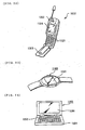
- the liquid crystal display device according to the present invention may be used as a display device in various types of electronic equipment, such as various display devices like televisions or monitors, communication equipment such as cellular telephones or PDAs, information processing devices such as personal computers, and so forth.
- various display devices like televisions or monitors
- communication equipment such as cellular telephones or PDAs
- information processing devices such as personal computers, and so forth.
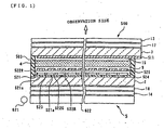
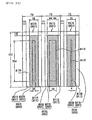
- this liquid crystal display device has a liquid crystal display panel (liquid crystal panel) 500 configured of a first substrate (upper substrate) 3 and a second substrate (lower substrate) 2 applied one to another across a seal member 503 with liquid crystal (a liquid crystal layer) 4 sandwiched therebetween, and an illumination device (a so-called back-light unit) 5 disposed at the second substrate 2 side of the liquid crystal display panel 500.
- the opposite side of the liquid crystal display panel 500 from the illumination device 5 as shown in Fig. 1 will be referred to as the "observation side”. That is to say, the "observation side” is the side at which an observer viewing images displayed on the liquid crystal display device is situated.
- the illumination device 5 has multiple LEDs 621 (only one is shown in Fig. 1 ) and a light guiding plate 622.
- the multiple LEDs 621 are arrayed facing the side edge of the light guiding plate 622, and cast light to this side edge face.
- the light guiding plate 622 is a plate-shaped member for guiding light from the LEDs 621 cast in from the side edge face to the substrate face of the liquid crystal display panel 500 (the surface of the second substrate 2) in a uniform manner.
- a scattering plate or the like is applied to the face of the light guiding plate 622 facing the liquid crystal display panel 500 to scatter the light cast out from the light guiding plate 622 to the liquid crystal display panel 500 in a uniform manner, while a reflecting plate is applied to the opposite side face for reflecting light heading in the opposite direction from the liquid crystal display panel 500, toward the liquid crystal display panel 500 (both omitted in the drawings).
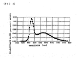
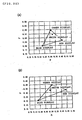
- Fig. 2 is a graph illustrating an example of spectral properties of the illumination light (the relation of the wavelength and luminance of the illumination light) irradiated to the liquid crystal display panel 500 from the illumination device 5.
- the horizontal axis shows the wavelength
- the vertical axis shows the luminance of the illumination light at each of the wavelengths, as a relative value wherein a predetermined luminance is set as "1.00" as a reference value.
- a case is assumed wherein there are irregularities in the luminance in the illumination light over the wavelengths within the visible light range, i.e., wherein the spectral properties of the illumination light are not uniform.
- the luminance of the illumination light according to the present embodiment is greatest at a wavelength close to 470 nm which corresponds to blue through green light, the luminance at around wavelengths 520 nm or above corresponding to yellow light through red light is comparatively weaker.
- the effects of the irregularities in the spectral properties in the light cast out at the observation side of the liquid crystal display panel 500 i.e., the light viewed by the observer.
- observation light the light viewed by the observer.
- the first substrate 3 and the second substrate 2 of the liquid crystal display panel 500 are plate-shaped transmissive members, such as glass or quartz, plastic, etc.
- the transparent electrodes 511 are formed on the inner surface (the liquid crystal 4 side) of the first substrate 3.
- the transparent electrodes 511 are band-shaped electrodes extending in a predetermined direction (the left and right directions in Fig. 1 ), and are formed of a transparent electroconductive material such as ITO (Indium tin Oxide) or the like.
- the surface of the first substrate 3 where the transparent electrodes 511 are formed is covered by an oriented film 15.
- This oriented film 15 is an organic thin film such as polyimide or the like, and has been subjected to rubbing processing for stipulating the orientation direction of the liquid crystal 4 when voltage is not applied.
- phase difference plate 17 and an upper polarization plate 13 are layered and disposed in that order on the first substrate 3.
- a reflective layer (transflective layer) 521 having multiple opening portions 521a is formed on the inter (liquid crystal 4 side) surface of the second substrate 2, of a material having reflecting light, such as aluminum or silver for example.
- the incidental light from the observation side of the liquid crystal display panel 500 is reflected at the surface of this transflective layer 521 (more specifically, at the surface other than the area where the opening portions 521a are formed) and is cast out at the observation side, thereby realizing a reflective display.
- the inner surface of the second substrate 2 is made to be coarse so as to form a scattering structure (unevenness) at the surface of the transflective layer 521, but this is omitted in the figures.
- a 1/4 wavelength plate 18 and a lower polarization plate 14 are disposed on the outer side (the surface of the outer side) of the second substrate 2.
- a color filter 522 (522R, 522G, 522B) and a shielding layer 523
- multiple transparent electrodes 525 and an oriented film 9 the same as the above-described oriented film 15.
- the transparent electrodes 525 are band-shaped electrodes formed on the surface of the overcoat layer 524 of a transparent electroconductive material.
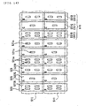
- Fig. 3 schematically shows the positional relation between the transparent electrodes 511 (shown by single-dot broken lines), on the first substrate 3, the transparent electrodes 525 on the second substrate 2, and the color filter 522.
- the transparent electrodes 525 extend in a direction intersecting the transparent electrodes 511 (vertical to the paper in Fig. 1 ).
- the liquid crystal 4 sandwiched between the first substrate 3 and second substrate 2 changes in orientation direction by voltage being applied between the transparent electrodes 511 and the transparent electrodes 525.
- sub-pixels 551 (551R, 551G, 551B)". That is to say, the sub-pixels 551 can also be described as the smallest units of areas wherein the orientation of liquid crystal changes according to application of voltage.
- the shielding layer 523 is formed in a lattice-like shape so as to cover the gap portions between the sub-pixels 551 arrayed in matrix fashion (that is to say, areas other than the areas where the transparent electrodes 511 and the transparent electrodes 525 face one another), serving to shield the gaps between the sub-pixels 551.
- the color filter 522 is a layer formed of a resin material or the like corresponding to the sub-pixels 551, and as shown in Fig. 3 , is colored, with a dye or pigment, either R (red), G (green), or B (blue).
- sub-pixels corresponding to the color filters 522R, 522G, and 522B will respectively be referred to as sub-pixels 551R, 551G, and 551B.
- These three sub-pixels 551R, 551G, and 551B with mutually differing colors form a pixel (dot) 615, which is the smallest unit of the display image.
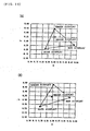
- Fig. 4 is a graph representing the transmittance ratio properties of each of the color filters 522R, 522G, and 522B, with the horizontal axis as the wavelength of incident light to the color filter 522, and the vertical axis as transmittance ratio (the percentage of light emitted as to the amount of incident light).
- the color filter 522R exhibits high transmittance ratio for light having a wavelength 600 nm or more which corresponds to red
- the color filter 522G exhibits high transmittance ratio for light having a wavelength of 500 through 600 nm which corresponds to green
- the color filter 522B exhibits high transmittance ratio for light having a wavelength of 400 through 500 nm which corresponds to blue light.
- the opening portions 521a are provided near the center of each of the sub-pixels 551 on the transflective layer 521. Illumination light form the illumination device 5 passes through the opening portions 521a and is emitted from the observation side of the liquid crystal display panel 500, thereby realizing transmissive display.
- the area of the sub-pixels 551 the area corresponding to the opening portions 521a, i.e., the area through which illumination light from the illumination device 5 passes, will be referred to as "transmitting area (transmissive area)".
- the opening portions 521a formed on the transflective layer 521 have the area thereof selected such that the area of the transmissive areas mutually differ for each of the three sub-pixels 551R, 551G, and 551B, making up each pixel 615. More specifically, the area of the opening portions 521a corresponding to each of the sub-pixels 551R, 551G, and 551B corresponds to the spectral properties of the illumination light emitted from the illumination device 5.
- the luminance of the wavelengths from blue light to green light is great, while the luminance of the wavelength corresponding to red light is comparatively small. Accordingly, with regard to the sub-pixels 551G where the green color filter 522G corresponding to the wavelength with the greatest luminance, the area of the opening portion 521a corresponding thereto is formed smaller in comparison to the sub-pixels 551R and 551B corresponding to the other colors.
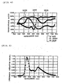
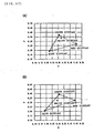
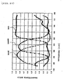
- Fig. 5 is a graph illustrating the spectral properties of the observed light emitting to the observation side from the liquid crystal display panel 500 in the event that transmissive display is carried out with the above-described configuration.
- Fig. 6 illustrates the spectral properties of the observed light in the event that transmissive display is carried out with an arrangement wherein all transmissive areas are of the same area for all sub-pixels 551 (hereafter referred to as "conventional configuration"), as a comparative example with that shown in Fig. 5 .
- the spectral properties of the observed light in the event that transmissive display is carried out using the illumination light having the spectral properties shown in Fig. 2 is shown.
- Fig. 2 the illumination light having the spectral properties shown in Fig. 2
- the horizontal axis shows the wavelength
- the vertical axis shows the luminance of the illumination light at each of the observed light, in a relative manner wherein a predetermined luminance (the same luminance in both Fig. 5 and Fig. 6 ) is set as "1.00" as a reference value.
- the observed light visually recognized by the observer is light which has an extremely high luminance near the wavelength 470 nm. Accordingly, the image light visually recognized by the observer will be a blue-greenish image.
- the luminance in the observed light near the wavelength 470 nm is comparatively lower than that in the case shown in Fig. 6 , as shown in Fig. 5 .
- the illumination light light at wavelengths with relatively small luminance is sufficiently allowed to pass through the transflective layer 521, while passage of light at wavelengths with relatively great luminance through the transflective layer 521 is restricted, thereby suppressing the effects which irregularities in the spectral properties of the illumination light have on the observed light.
- the non-uniformity in the spectral properties of the illumination light is compensated for, so that good color reproduction can be realized.
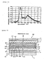
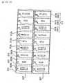
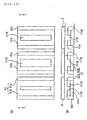
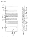
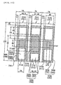
- Fig. 7 is a cross-sectional view schematically showing an example of the configuration of the liquid crystal display device according to the present embodiment
- Fig. 8 is a perspective diagram illustrating the configuration of the principal components of the liquid crystal display panel making up the liquid crystal display device.
- the cross-section along A-A' in Fig. 8 is equivalent to Fig. 7 .
- multiple pixel electrodes 513 arrayed in matrix fashion, and multiple scanning lines 514 extending in a predetermined direction (the direction vertical to the paper in Fig. 7 ) in the gap portions of the pixel electrodes 513, are formed on the inner side surface of the first substrate 3.
- Each of the pixel electrodes 513 are formed of a transparent electroconductive material such as ITO or the like, for example.
- each of the pixel electrodes 513 and the scanning lines 514 adjacent to the pixel electrodes 513 are connected by TFDs 515.
- Each of the TFDs 515 are two-terminal switching devices having non-linear current/voltage properties.
- a transflective layer 521 having multiple opening portions 521a, a color filter 522 and a shielding layer 523, an overcoat layer 524 for covering the surface of the second substrate 2 where these are formed.
- multiple data lines 527 extending in a direction intersecting with the scanning lines 514 are formed on the surface of the overcoat layer 524.
- the data lines 527 are band-shaped electrodes formed of an transparent electroconductive material.
- Fig. 9 shows the positional relation between the pixel electrodes 513 (shown by single-dot broken lines) and the data lines 527.
- the data lines 527 face the multiple pixel electrodes 513 arrayed in rows on the first substrate 3.
- the liquid crystal 4 sandwiched between the electrodes changes in orientation state by voltage being applied between the pixel electrodes 513 on the first substrate 3 and the data lines 527 on the second substrate 2.
- the areas where the pixel electrodes 513 and the data lines 527 face one another are equivalent to the sub-pixels 551 (more specifically, sub-pixels 551R, 551G, and 551B, corresponding to the respective color filters 522R, 522G, and 522B).
- opening portions 521a are formed at positions corresponding to near the center portion of each of the sub-pixels 551 on the transflective layer 521 with the present embodiment as well, as shown in Fig. 9 .
- the area of each of the opening portions 521a is determined such that the percentage of the transmissive area in each of the sub-pixels 551R, 551G, and 551B, is a percentage corresponding to the spectral properties of the illumination light from the illumination device 5.
- the present embodiment also assumes performing transmissive display using the illumination light having the spectral properties shown in Fig. 2 above.
- the area of the opening portion 521a corresponding thereto is smaller in comparison to the area of the opening portions 521a corresponding to the sub-pixels 551R or 551B corresponding to the other colors.
- the percentage of the transmissive area in the sub-pixel 551G is smaller than the percentage of the transmissive areas in the sub-pixels 551R or 551B of the other colors.
- the area of the opening portion 521a corresponding thereto is greater and the percentage of transmissive area in the sub-pixel 551R is greater in comparison to that of the sub-pixels 551G or 551B of the other colors.
- the area ratio of the opening portions 521a in the sub-pixels 551R, 551G, and 551B is "4 : 1 : 2".
- transmissive areas are areas following the edges of the sub-pixels 551.
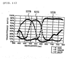
- Fig. 10 is a cross-section diagram illustrating the configuration of the liquid crystal display device according to the present embodiment.
- the liquid crystal panel 500 according to the present embodiment differs from the liquid crystal panel 500 described in the above embodiments in that the color filter 522 (522R, 522G, 522B), shielding layer 523, and overcoat layer 524 are formed on the first substrate 3, and in that the transparent electrodes 511 and oriented film 15 are formed on the surface of the overcoat layer.
- the transmittance ratio properties of the color filter 522 according to the present embodiment differs from the transmittance ratio properties of the color filter 522 according to the above-described embodiments shown in Fig. 4 .
- Fig. 11 is a graph illustrating the transmittance ratio properties of the color filters 522R, 522G, and 522B, according to the present embodiment.
- the color purity of the color filters 522 according to the present embodiment and particularly the color purity of the color filter 522G corresponding to the green color is higher than the color purity of the color filters 522 according to the above-described embodiments. More specifically, this is as follows.
- Tmax/Tmin the maximum transmittance ratio of each of the color filters 522 in the wavelength range of 380 nm through 780 nm and Tmin represents the minimum transmittance ratio in the same wavelength range, as a parameter for evaluating color purity that is to say, the greater the numerical value Tmax/Tmin is, the higher the color purity).
- Tmax/Tmin of the green color filter 522G shown in the above-described Fig.
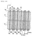
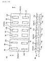
- the form of the transflective layer 528 differs from that of the first and second embodiments. That is, in the above-described embodiments, examples of configuration were described wherein the form of the transflective layer 521 (more specifically, the form of the opening portions 521a in the transflective layer 521) is selected such that the areas positioned at the center of the sub-pixels serve as the transmissive areas. Conversely, with the present embodiment, the form of the transflective layer 528 is selected such that the areas following two opposing sides of the four sides defining each generally-rectangular-shaped sub-pixel 551 (the two sides extending in the Y direction) are made to be the transmissive areas. The following is a description of the specific form of the transflective layer 528, with reference to Fig. 12 .
- the transflective layer 528 according to the present embodiment has multiple portions extending in the Y direction on the second substrate 2.
- the transparent electrodes 525 are of the same form as that shown in the above-described embodiments, but differ in that they are formed so as to cover the transflective layer 528.
- the transflective layer 528 according to the present embodiment is formed in stripes so as to correspond to the transparent electrodes 525.
- transmissive portions (portions for transmitting illumination light from the illumination device) 528a are formed on the transflective layer 528 following the gap portions of the transparent electrodes 525.
- transmissive portions 528a formed thus being formed on the transflective layer 528 the areas following the opposing sides extending in the Y direction, of the four side defining the perimeter of the generally-rectangular-shaped sub-pixel 551, serve as transmissive areas, as shown in Fig. 12 .
- the form of the transflective layer 528 is selected such that the area of the transmissive area in at least one sub-pixel 551 differs from the area of the transmissive areas the other sub-pixels 551, as with the above-described first and second embodiments.
- a width Wr of a reflective layer corresponding to a row of sub-pixels 551R and a width Wb of a reflective layer corresponding to a row of sub-pixels 551B are approximately equal, and a width Wb of a reflective layer corresponding to a row of sub-pixels 551G is wider than the width Wr and the width Wb. Accordingly, the area Sr of the transmissive area in the sub-pixel 551R and the area Sb of the transmissive area in the sub-pixel 551B are approximately equal, while the area Sg of the transmissive area in the sub-pixel 551G is smaller than the area Sr or area Sb.
- the transmittance ratio of the green color filter 522G shown in the above embodiment is markedly higher as compared to the transmittance ratio of the other color filters 522R or 522b of the other colors. Accordingly, in order to perform ideal white display using the color filter 522 having the transmittance ratio properties shown in Fig. 4 (i.e., color reproduction compensation), there is the need to make the area of the transmissive area in the green sub-pixel 551G markedly smaller than the area of the transmissive area in the other color sub-pixels 551R or 551B. Conventionally, the transmittance ratio of the color filter 522G having the transmittance ratio properties shown in Fig.
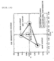
- Fig. 13 is a CIE chromaticity diagram indicating color coordinates of colors displayed by the liquid crystal display device according to the present embodiment.
- the color coordinates of colors displayed by a liquid crystal display device of a conventional configuration are shown as a comparative example with the present embodiment.
- a "conventional configuration" is a liquid crystal display device which uses a color filter having the transmittance ratio properties shown in Fig. 13 and has the same area for the transmissive areas for all sub-pixels.
- the color coordinates in the case of performing white display with the liquid crystal display device according to the present embodiment is closer to the ideal white display color coordinates as compared to the color coordinates in the case of performing white display with the liquid crystal display device according to the conventional configuration. That is to say, good color reproduction can be realized with the liquid crystal display device according to the present embodiment.
- the form of the transmissive areas of the sub-pixels i.e., the form of the transmissive portion (opening portion 521a or transmissive portion 528a) in the transflective layer 521 may be any form.
- the term "transmissive portion" in the present invention means "a portion in the transflective layer through which illumination light from the illumination device is transmitted", and is not restricted to opening portions (i.e., holes) formed in the transflective layer.
- the arrangement is such that the area of the opening portions 521a corresponding to the sub-pixels 551 is made to differ according to the spectral properties of the illumination light from the illumination device 5, but the arrangement may be as follows. That is, as shown in Fig. 14 , the area of the opening portions 521a provided in the transflective layer 521 are generally the same, while on the other hand, the number of opening portions 521a provided for each sub-pixel 551 is of a number according to the spectral properties of the illumination light.
- the area ratio of the opening portions 521a corresponding to the sub-pixels 551R, 551G, and 551B is "4 : 1 : 2" to correspond to the spectral properties of the illumination light illustrated in Fig. 2 above, but with the present modification, the ratio of the number of the opening portions 521a corresponding to the sub-pixels 551R, 551G, and 551B, is made to be "4 : 1 : 2", as shown in Fig. 4 .
- the same advantages as those of the above embodiments can be obtained with this configuration as well.
- the opening portions 521a can be scattered throughout the sub-pixels 551, and thus is advantageous in that such problems can be avoided.
- the percentage of transmissive area in the sub-pixels 551 is made to differ for each of the sub-pixels 551 corresponding to the same color. Irregularities in the spectral properties of the illumination light can be sufficiently compensated for with this configuration in the event that the spectral properties of the illumination light from the illumination device 5 are the same through the entire face of the substrate surface of the liquid crystal display panel 500. However, there may be cases wherein the spectral properties of the illumination light from the illumination device 5 differ according to places in the substrate face. For example, some places in the substrate face may be irradiated with illumination light having the spectral properties shown in Fig. 2 , while other places may be irradiated with illumination light having spectral properties other than those shown in Fig. 2 .
- the percentage of the transmissive area may be changed according to the position of the sub-pixels 551 in the substrate face (i.e., the area of the opening portions 521a may be made to differ).
- the area ratio of the transmissive area in the sub-pixels 551R, 551G, and 551B may be "4 : 1 : 2" at a pixel 615 situated at a position wherein illumination light having to the spectral properties illustrated in Fig.
- the area ratio of the transmissive area in the sub-pixels 551R, 551G, and 551B may be "3 : 1 : 2" at a pixel 615 situated at a position wherein illumination light having somewhat less luminance in the blue light through the green light as compared to the above illumination light is irradiated.
- the percentage of the transmissive area of the sub-pixels 551 corresponding to the same color is all the same throughout the sub-pixels 551.
- non-uniformity of spectral properties of the illumination light in the substrate face can be compensated for, and thus is advantageous in that color reproduction can be improved in a more sure manner.
- the advantages of compensating for irregularities in the spectral properties of the illumination light can be compensated for and good color reproduction can be realized, by setting the area according to the spectral properties of the illumination light, such as making the area of the transmissive area in sub-pixels of a color corresponding to a wavelength of the illumination light with great luminance to be smaller than the area of the transmissive area in sub-pixels of a color corresponding to a wavelength with less luminance.
- the area of the transmissive area of the sub-pixels does not necessarily need to be according to the spectral properties of the illumination light. For example, arranging for the area of the transmissive area in the sub-pixels 551G corresponding to green or the area of the transmissive area in the sub-pixels 551B corresponding to blue (i.e., the area of the opening portions 521a corresponding to these sub-pixels 551) to be greater than the area of the transmissive area in the sub-pixels 551R corresponding to red regardless of the spectral properties of the illumination light enables the display to be intentionally made blue-greenish.
- the area of the opening portion 521a in the transflective layer 521 be set such that the area of the transmissive area for one sub-pixel 551 to be different from the area of the transmissive area for another sub-pixel 551.
- the form of the transflective layer 528 is selected such that the areas following two opposing sides of the four sides defining each sub-pixel are made to be the transmissive areas, but the form of the transflective layer 528 may be selected such that the area following one side, three sides, or all sides (four sides) of the four sides is used as the transmissive area. That is to say, in the forming the transmissive area of the area following the edges of the sub-pixel, all that is necessary is to make an area following at least one of the multiple sides defining the sub-pixels to be the transmissive area. Also, in the third embodiment, an example is given of a transflective layer 528 with a form of being connected ling multiple sub-pixels 551, but the transflective layer 528 may be of a form separated for each pixel 551.]
- the above embodiments illustrate an example of a case wherein the transflective layer 521 is formed on the inner surface of the second substrate 2, but an arrangement may be conceived wherein the transflective layer 521 is formed on the outer surface of the second substrate 2. In short, a configuration wherein the transflective layer 521 is situated at the opposite side of the liquid crystal 4 as to the observation side will suffice.
- the applicable scope of the present invention is not restricted to this, and can also be applied to liquid crystal display devices using three-terminal switching devices, of which TFTs (Thin Film Transistor) are representative.
- TFTs Thin Film Transistor
- an opposing electrode is formed on the entire face of one substrate, while multiple scanning lines and multiple data lines are formed on the other substrate so as to be extended in the directions of mutually intersecting, and pixel electrodes connected to both of these via TFTs are arrayed in matrix fashion.
- the areas where the pixel electrodes and the opposing electrode face one another function as the sub-pixels.
- the transflective layer 521 and the transparent electrodes 525 are formed separately, but an arrangement may be made wherein an electrode for applying voltage to the liquid crystal 4 is formed of an electroconductive material having light-reflecting properties, so that this electrode also functions as the transflective layer 521. That is, as shown in Fig. 1 , the transflective layer 521 is not provided, and a reflecting electrode of the same form as the transparent electrode 525 is provided in the stead thereof.
- opening portions of the forms illustrated as examples in the above embodiments and modifications are provided at a portion of the areas of the reflecting electrode corresponding to the sub-pixels (i.e., the areas facing the transparent electrode 511 on the first substrate 30).
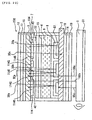
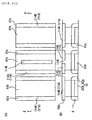
- Fig. 15 is a diagram illustrating an example of a non claimed liquid crystal display device, and is a partial cross-sectional diagram illustrating an example of a passive matrix transflective color liquid crystal display device wherein a color filter is provided on the inner side of the lower substrate.
- Fig. 16 is a diagram illustrating only the transflective layer and color filter and shielding film of the liquid crystal display device shown in Fig. 15 , wherein Fig. 16(A) is a plan view for describing the overlapping of the transflective layer and the color filter, and Fig. 16(B) is a cross-sectional view along A-A' shown in Fig. 16(A) .
- the liquid crystal display device shown in Fig. 15 has a schematic configuration comprising a liquid crystal panel (liquid crystal display panel) 1, and a back-light (illumination device) disposed at the rear side of the liquid crystal panel 1 (at the outer side of the lower substrate 2).
- the liquid crystal panel 1 has a schematic configuration comprising a liquid crystal layer 4 of an STN (Super Twisted Nematic) liquid crystal or the like sandwiched between the lower substrate 2 and upper substrate 3 disposed facing one another.
- STN Super Twisted Nematic
- the lower substrate 2 is formed of glass or resin or the like, with a transflective layer 6 disposed on the inner face side of the lower substrate 2, having a color filter 10 layered on the upper side of the with transflective layer 6, with a shielding film 41 of a black-colored resin material or the like provided between the pigment layers 11R, 11G, and 11B making up the color filter 10. Also, a transparent smoothing film 12 for smoothing the unevenness formed by the color filter 10 is layered on the color filter 10.
- stripe-shaped transparent electrodes (segment electrodes) 8 formed of a transparent electroconductive film such as indium tin oxide (hereafter referred to as "ITO") or the like are extended in the vertical direction to the paper on the smoothing film 12, and an oriented film 9 of polyimide or the like is disposed above the transparent electrodes 8 so as to cover the transparent electrodes 8.
- ITO indium tin oxide
- a 1/4 wavelength plate 18, a lower polarization plate 14, and a reflecting polarizer 19, are disposed on the outer side of the lower substrate 2.
- the upper substrate 3 is formed of glass or resin or the like, with stripe-shaped transparent electrode (common electrode) 7 formed of a transparent electroconductive film such as ITO or the like on the inner side of the upper substrate 3, extending in the direction orthogonal to the transparent electrodes 8 provided on the lower substrate 2 (the sideways direction in the drawing), having an oriented film 15 of polyimide or the like disposed below the transparent electrode 7 so as to cover the transparent electrode 7.
- stripe-shaped transparent electrode (common electrode) 7 formed of a transparent electroconductive film such as ITO or the like on the inner side of the upper substrate 3, extending in the direction orthogonal to the transparent electrodes 8 provided on the lower substrate 2 (the sideways direction in the drawing), having an oriented film 15 of polyimide or the like disposed below the transparent electrode 7 so as to cover the transparent electrode 7.
- a forward scattering plate 16, a phase difference plate 17, and an upper polarization plate 13 are layered and disposed in that order on the upper substrate 3.
- a reflecting plate 51 is disposed on the lower face side of the back-light 5 (the opposite side from the liquid crystal panel 1).
- the transflective layer 6 is formed of a metal film with high reflectivity such as aluminum or the like, and as shown in Fig. 16 , is formed by opening the metal film in the form of windows, having, for each pixel, transmissive areas 6a for transmitting light emitted from the back-light 5 and incident light from the upper substrate 3 side, and a reflective area 6b for reflecting incident light from the upper substrate 3 side.
- the color filter 10 is provided corresponding to each pixel making up the display area, with the red layer 11R and green layer 11G and blue layer 11B extending in the direction vertical to the paper so as to be orthogonal to the transparent electrode 7 provided on the upper substrate 3 described above, having pigment layers repeatedly arrayed in the order of the red layer 11R, green layer 11G, and blue layer 11B.
- the pigment layers 11R, 11G, and 11B are provided on the entirety of the area overlapping the transmissive areas 6a of the transflective layer 6 in a planar manner, and an area excluding a part of an area overlapping the reflective area 6b in a planar manner by opening the pigment layers 11R, 11G, and 11B in window fashion, as shown in Fig. 16 .
- the color filter 10 comprises a pigment layer formation area wherein the pigment layers 11R, 11G, and 11B are provided, and pigment layer non-formation areas 11D, 11E, and 11F which are a part of an area overlapping with the reflective area 6b in a planar manner but where the pigment layers 11R, 11G, and 11B are not provided.
- the area of the pigment layer formation area i.e., the area of the pigment layers 11R, 11G, and 11B, is set such that the red layer 11R, blue layer 11B, and green layer 11G are smaller in that order.
- the reflected light there is light 30a which passes through the pigment layers 11R, 11G, and 11B, and light 30b which passes through the pigment layer non-formation areas 11D, 11E, and 11F, wherein only the light 30a which has passed through the pigment layers 11R, 11G, and 11B is colored, and the light 30b which has passed through the pigment layer non-formation areas 11D, 11E, and 11F is not colored.
- the light emitted externally from the upper substrate 3 side when in the reflective mode is the sum of the colored light 30a which has passed through the pigment layers 11R, 11G, and 11B and the uncolored light 30b which has passed through the pigment layer non-formation areas 11D, 11E, and 11F.
- the light 50a cast into the liquid crystal display device from the back-light 5 when in the transmissive mode passes through the transmissive areas 6a, passes through the pigment layers 11 of the color filter 10, and is colored. Also, the light 50b cast into the liquid crystal display device from the back-light 5 when in the transmissive mode is shielded by the transflective layer 6.
- the light emitted externally from the upper substrate 3 side when in the transmissive mode becomes light 50a which has passed through the pigment layers 11 of the color filter 10 once and is colored.
- the light obtained when in the reflective mode is the sum of the uncolored light 30b which has passed through the pigment layer non-formation areas 11D, 11E, and 11F and the colored light 30a which has passed through the pigment layers 11.
- the light obtained when in the transmissive mode is only the light 50a which passes through the pigment layer 11 and is colored.
- the difference in concentration between the light obtained by passing through the color filter 10 twice when in the reflective mode and the light obtained by passing through the color filter 10 once when in the transmissive mode can be reduced.
- the pigment layer 11 is formed of the red layer 11R, green layer 11G, and blue layer 11B, with the area of the pigment layers 11R, 11G, and 11B being such that the red layer 11R, blue layer 11B, and green layer 11G are smaller in that order, and the color properties of the color filter 10 are adjusted by changing the area of the pigment layers 11R, 11G, and 11B, so that the color reproduction can be improved even further, and a liquid crystal display device having even more excellent display quality can be realized.
- the liquid crystal display device shown in Fig. 15 has a transparent film 12 for smoothing the steps between the areas where the pigment layers 11R, 11G, and 11B are provided and the pigment layer non-formation areas 11D, 11E, and 11F, so adverse effects due to steps between the areas where the pigment layers 11R, 11G, and 11B are provided and the pigment layer non-formation areas 11D, 11E, and 11F can be avoided, thereby improving the reliability of the liquid crystal display device.
- the transflective layer fabricated with a thin metal film absorbs light in addition to reflecting and transmitting light, but with the liquid crystal display device shown in Fig. 15 , the transflective layer 6 is opened in a window-like manner, thereby forming the transmissive areas 6a, so there is no absorbing of light, thereby enabling improving of the reflectivity and transmittance ratio.
- the overall configuration of the liquid crystal display device is the same as the fourth non claimed embodiment shown in Fig. 15 , and accordingly detailed description will be omitted.
- the point where the liquid crystal display device according to the fifth embodiment differs from the liquid crystal display device according to the fourth embodiment is only the form of the transflective layer and the color filter, so description of the transflective layer and the color filter will be given in detail with reference to Fig. 17 .
- Fig. 17 is a diagram illustrating only the transflective layer and the color filter and the transparent electrodes on the lower substrate in the liquid crystal display device according to the fifth embodiment, wherein Fig. 17(A) is a plan view for describing the overlapping of the transflective layer and the color filter, and Fig. 17(B) is a cross-sectional diagram following line C-C' shown in Fig. 17(A) .
- the transflective layer 61 is extended and provided in a stripe form in the direction vertical to the paper so as to be orthogonal to the transparent electrode 7 provided on the upper substrate 3, and provided with the same pitch as the transparent electrodes 8 provided on the lower substrate 2. Then, as shown in Fig.
- the width of the pattern of the transparent electrodes 8 provided on the lower substrate 2 is formed so as to be greater than the width of the metal film pattern making up the transflective layer 61, so that band-shaped areas where the metal film making up the transflective layer 61 and the transparent electrodes 8 do not overlap in a parallel manner serve as transmissive areas 61a, and the entire area where the metal film is provided serves as a reflective area 61b.
- the color filter 101 is provided for each of the pixels making up the display area, with the red layer 111R and green layer 111G and blue layer 111B extending in the direction vertical to the paper so as to be orthogonal to the transparent electrode 7 provided on the upper substrate 3, having pigment layers 111 repeatedly arrayed in the order of the red layer 111R, green layer 111G, and blue layer 111B.
- the pigment layers 111R, 111G, and 111B are provided on the entirety of the area overlapping the transmissive areas 61a of the transflective layer 61 in a planar manner, and an area excluding a part of an area overlapping the reflective area 61b of the transflective layer 61 in a planar manner by opening the pigment layers 111R, 111G, and 111B in stripe forms.
- the color filter 101 existing in the color filter 101 are a pigment layer formation area where the pigment layers 111R, 111G, and 111B are formed, and pigment layer non-formation areas 111D, 111E, and 111F which are a part of an area overlapping with the reflective area 61b in a planar manner where the pigment layers 111R, 111G, and 111B are not provided.
- the area of the pigment formation area i.e., the area of the pigment layers 111R, 111G, and 111B, is set such that the red layer 111R, blue layer 111B, and green layer 111G are smaller in that order, as with the fourth embodiment.
- Such a liquid crystal display device also has pigment layer non-formation areas 111D, 111E, and 111F at a part of an area overlapping with the reflective area 61b of the transflective layer 61 in a planar manner, as with the fourth embodiment, so a part of the external light cast into the liquid crystal display device when in the reflective mode passes through the pigment layer non-formation areas 111D, 111E, and 111F, and the light obtained by passing trough the color filter 101 twice when in the reflective mode is the sum of the uncolored light which has passed through the pigment layer non-formation areas 111D, 111E, and 111F and the colored light which has passed through the pigment layers 111.
- the pigment layer 111 is formed of the red layer 111R, green layer 111G, and blue layer 111B, with the area of the pigment layers 111R, 111G, and 111B being such that the red layer 111R, blue layer 111B, and green layer 111G are smaller in that order, and the color properties of the color filter 101 are adjusted by changing the area of the pigment layers 111R, 111G, and 111B, so that the color reproduction can be improved even further, and a liquid crystal display device having even more excellent display quality can be realized.
- the width of the pattern of the transparent electrodes 8 provided on the lower substrate 2 is formed so as to be greater than the width of the metal film pattern making up the transflective layer 61, thereby forming band-shaped transmissive areas 61a and reflective areas 61b are formed, so irregularities in the longitudinal direction of the openings are reduced as compared to a transflective layer with window-like openings, and accordingly this is stable from the perspective of manufacturing.
- Fig. 18 is a diagram illustrating an example of another non claimed liquid crystal display device and is a partial cross-sectional view illustrating an example of a passive matrix transflective color liquid crystal display device wherein a color filter is provided on the inner side of the upper substrate.
- Fig. 19 is a diagram illustrating only the transflective layer and color filter and shielding film of the liquid crystal display device shown in Fig. 18 , wherein Fig. 19(A) is a plan view for describing the overlapping of the transflective layer and the color filter, and Fig. 19(B) is a cross-sectional view along B-B' shown in Fig. 19(A) .
- the liquid crystal display device shown in Fig. 18 has a schematic configuration comprising a liquid crystal panel 100 and a back-light (illumination device) 5 disposed at the rear side of the liquid crystal panel 100 (at the outer side of the lower substrate 2).
- the liquid crystal panel 100 has a schematic configuration comprising a liquid crystal layer 4 sandwiched between the lower substrate 2 and upper substrate 3 disposed facing one another, as with the fourth embodiment.
- the lower substrate 2 has formed on the inner side thereof a transflective layer 6 and an insulating film 23 in that order, with a stripe-shaped transparent electrode 8 (a common electrode here) formed of a transparent electroconductive film such as ITO or the like extending sideways in the drawing upon the insulating film 23, and an oriented film 9 of polyimide or the like disposed above the transparent electrode 8 so as to cover the transparent electrode 8.
- a stripe-shaped transparent electrode 8 (a common electrode here) formed of a transparent electroconductive film such as ITO or the like extending sideways in the drawing upon the insulating film 23, and an oriented film 9 of polyimide or the like disposed above the transparent electrode 8 so as to cover the transparent electrode 8.
- a 1/4 wavelength plate 18, a lower polarization plate 14, and a reflecting polarizer 19, are disposed on the outer side of the lower substrate 2, as with the fourth embodiment.
- a color filter 20 is layered on the inner side of the upper substrate 3, with a shielding film 42 of a black-colored resin material or the like provided between the pigment layers 21R, 21G, and 21B making up the color filter 20.
- a transparent smoothing film 22 for smoothing the unevenness formed by the color filter 20 is layered below the color filter 20.
- stripe-shaped transparent electrodes (segment electrodes here) 7 formed of a transparent electroconductive film such as ITO or the like are extended in a direction orthogonal to the transparent electrode 8 disposed on the lower substrate 2 (in the vertical direction to the paper) under the smoothing film 22, and an oriented film 15 is disposed below the transparent electrodes 7 so as to cover the transparent electrodes 7.
- a forward scattering plate 16, a phase difference plate 17, and an upper polarization plate 13 are layered and disposed in that order on the outer side of the upper substrate 3, as with the fourth embodiment.
- a reflecting plate 51 is disposed on the lower face side of the back-light 5 (the opposite side from the liquid crystal panel 1), as with the fourth embodiment.
- the transflective layer 6 is formed by opening metal film in the form of windows, having, for each pixel, transmissive areas 6a and a reflective area 6b.
- the color filter 20 has the red layer 21R and green layer 21G and blue layer 21B extending in the direction vertical to the paper so as to be orthogonal to the transparent electrode 8 provided on the lower substrate 2, having pigment layers 21 repeatedly arrayed in the order of the red layer 21R, green layer 21G, and blue layer 21B.
- the pigment layers 21R, 21G, and 21B are provided on the entirety of the area overlapping the transmissive areas 6a of the transflective layer 6 in a planar manner, and an area excluding a part of an area overlapping the reflective area 6b of the transflective layer 6 in a planar manner, by opening the pigment layers 21R, 21G, and 21B, in window fashion.
- the color filter 20 comprises a pigment layer formation area wherein the pigment layers 21 are provided, and pigment layer non-formation areas 21D, 21E, and 21F which are a part of an area overlapping with the reflective area 6b in a planar manner but where the pigment layers 21R, 21G, and 21B are not provided.
- the area of the pigment formation area i.e., the area of the pigment layers 21R, 21G, and 21B, is set such that the red layer 21R, blue layer 21B, and green layer 21G are smaller in that order, as with the fourth embodiment.
- the light emitted externally from the upper substrate 3 side in the reflective mode is the sum of the uncolored light 30b and the colored light 30b.
- the light externally emitted from the upper substrate 3 side in the transmissive mode also becomes colored light 50a which has passed through the pigment layers 21 of the color filter 20 once, as with the fourth embodiment.
- the difference in concentration between the light obtained by passing through the color filter 20 twice when in the reflective mode and the light obtained by passing through the color filter 20 once when in the transmissive mode can be reduced.
- the pigment layer 21 is formed of the red layer 21R, green layer 21G, and blue layer 21B, with the area of the pigment layers 21R, 21G, and 21B being such that the red layer 21R, blue layer 21B, and green layer 21G are smaller in that order, and the color properties of the color filter 20 are adjusted by changing the area of the pigment layers 21R, 21G, and 21B, so that the color reproduction can be improved even further, and a liquid crystal display device having even more excellent display quality can be realized.
- Fig. 20 is a diagram illustrating an example of another non claimed liquid crystal display device , and is a partial cross-sectional view illustrating an example of a passive matrix transflective liquid crystal display device wherein transparent electrodes are directly provided on the transflective layer.
- Fig. 21 is a diagram illustrating only the transflective layer and color filter and transparent electrodes on the lower substrate, in the liquid crystal display device shown in Fig. 20 , wherein Fig. 21(A) is a plan view for describing the overlapping of the transflective layer and the color filter, and Fig. 21(B) is a cross-sectional view along D-D' shown in Fig. 21(A) .
- the liquid crystal display device shown in Fig. 20 has a schematic configuration comprising a liquid crystal panel 200 and a back-light (illumination device) 5 disposed at the rear side of the liquid crystal panel 200 (at the outer side of the lower substrate 2).
- the liquid crystal panel 200 has a schematic configuration comprising a liquid crystal layer 4 sandwiched between the lower substrate 2 and upper substrate 3 disposed facing one another, as with the fourth embodiment.
- the lower substrate 2 has formed on the inner side thereof a transflective layer 62 formed of a metal film with high reflectance such as aluminum or the like, and stripe-shaped transparent electrodes 8 (segment electrodes here) disposed directly on the transflective layer 62 and formed of a transparent electroconductive film such as ITO or the like, both extending vertically in the drawing, and an oriented film 9 disposed above the transparent electrodes 8 so as to cover the transparent electrodes 8.
- a transflective layer 62 formed of a metal film with high reflectance such as aluminum or the like
- stripe-shaped transparent electrodes 8 stripegment electrodes here
- a transparent electroconductive film such as ITO or the like
- a 1/4 wavelength plate 18, a lower polarization plate 14, and a reflecting polarizer 19, are disposed on the outer side of the lower substrate 2, as with the fourth embodiment.
- a color filter 104 is layered on the inner side of the upper substrate 3, with a shielding film 43 provided between the pigment layers 114R, 114G, and 114B making up the color filter 104.
- a transparent smoothing film 32 for smoothing the unevenness formed by the color filter 104 is layered below the color filter 104.
- a stripe-shaped transparent electrode (a common electrode here) 7 formed of a transparent electroconductive film ITO or the like is extended in a direction orthogonal to the transparent electrodes 8 disposed on the lower substrate 2 (in the sideways direction to the paper) under the smoothing film 32, and an oriented film 15 is disposed below the transparent electrode 7 so as to cover the transparent electrode 7.
- a forward scattering plate 16, a phase difference plate 17, and an upper polarization plate 13 are layered and disposed in that order on the upper substrate 3, as with the fourth embodiment.
- a reflecting plate 51 is disposed on the lower face side of the back-light 5 (the opposite side from the liquid crystal panel 1), as with the fourth embodiment.
- the transflective layer 62 is provided with the same pitch as the transparent electrodes 8 provided on the lower substrate 2, and as shown in Fig. 21(B) , the width of the pattern of the transparent electrodes 8 provided on the lower substrate 2 is formed so as to be greater than the width of the metal film pattern making up the transflective layer 62, so that band-shaped areas where the metal film making up the transflective layer 62 and the transparent electrodes 8 do not overlap in a planar manner serve as transmissive areas 62a, and the entire area where the metal film is provided serves as a reflective area 62b.
- the color filter 104 is provided corresponding to each of the pixels making up the display area as with the fourth embodiment, and has the red layer 114R and green layer 114G and blue layer 114B extending in the direction vertical to the paper so as to be orthogonal to the transparent electrode 7 provided on the upper substrate 3, having pigment layers 114 repeatedly arrayed in the order of the red layer 114R, green layer 114G, and blue layer 114B.
- the green layer 114G is provided on the entirety of the area overlapping the transmissive areas 62a of the transflective layer 62 in a planar manner, and an area excluding a part of an area overlapping the reflective area 62b of the transflective layer 62 in a planar manner by opening the green layer 114G in stripe fashion.
- the color filter 104 comprises a pigment layer formation area wherein the pigment layers 114R, 114G, and 114B are provided, and a pigment layer non-formation area 114E which is a part of an area overlapping with the reflective area 62b in a planar manner but where the green layer 114G is not provided.
- the area of the pigment formation area i.e., the area of the pigment layers 114R, 114G, and 114B, is set such that the red layer 114R, blue layer 114B, and green layer 114G are smaller in that order.
- the light which is emitted externally from the upper substrate 3 side in the reflective mode there is light 30a which passes through the pigment layers 114R, 114G, and 114B, and light 30b which passes through the pigment layer non-formation area 114E, wherein only the light 30a which has passed through the pigment layers 114R, 114G, and 114B is colored, and the light 30b which has passed through the pigment layer non-formation area 114E is not colored.
- the light emitted externally from the upper substrate 3 side when in the reflective mode is the sum of the uncolored light 30b and the colored light 30b.
- the light externally emitted from the upper substrate 3 side in the transmissive mode also becomes colored light 50a which has passed through the pigment layers 114 of the color filter 104 once, as with the fourth embodiment.
- the difference in concentration between the light obtained by passing through the color filter 104 twice when in the reflective mode and the light obtained by passing through the color filter 104 once when in the transmissive mode can be reduced.
- the pigment layer 114 is formed of the red layer 114R, green layer 114G, and blue layer 114B, with the area of the pigment layers 114R, 114G, and 114B being such that the green layer 114G is smaller than the red layer 114R and blue layer 114B, and the color properties of the color filter 104 are adjusted by changing the area of the green layer 114G, so that the color reproduction can be improved even further, and a liquid crystal display device having even more excellent display quality can be realized.
- the pigment layer non-formation area 114E is dependent on only the green layer 114G which contributes to colorization of green which is the most visually effective color, so excellent colorization can be obtained, and deterioration of reflectance due to providing the pigment layer non-formation area 114E can be reduced.
- the transparent electrodes 8 formed of a transparent electroconductive film are directly disposed on the transflective layer 62 formed of metal film, so the resistance value of the transparent electrodes 8 can be reduced thereby reducing chrominance non-uniformity in display.
- the overall configuration of the liquid crystal display device is the same as the fourth non claimed embodiment shown in Fig. 15 , and accordingly detailed description will be omitted.
- the liquid crystal display device according to the eighth embodiment has different area for the transmissive areas of the sub-pixels as with the above-described first embodiment, and also is formed so that the area of the pigment layer non-formation areas in the pigment layer differ as with the above-described fourth embodiment. Accordingly, detailed description of the configurations which are the same as the liquid crystal display device according to the first embodiment and the liquid crystal display device according to the fourth embodiment will be omitted, and description of the forms of the transflective layer and color filter which are the characteristic parts of the liquid crystal display device according to the eighth embodiment will be given in detail, with reference to the drawings.
- Fig. 32 is a diagram illustrating the transflective layer and color filter of the liquid crystal display device according to the eighth embodiment, and is a diagram corresponding to Fig. 16(A) described with the fourth embodiment.
- reference numeral 703 denotes a transflective layer.
- the transflective layer 703 has, for each pixel, transmissive areas 701 formed by opening the metal film in window fashion for light emitted from the back-light 5 or incident light from the upper substrate 3 to pass through, and reflective area 702 (hatched diagonally upwards toward the right in Fig. 32 ) for reflecting incident light from the upper substrate 3, as with the fourth embodiment.
- the transflective layer 703 is such that the area of the opening portions corresponding to each of the sub-pixels 751R, 751G, and 751B, making up each pixel 751, that is to say, the area of the transmissive areas 701R, 701G, and 701B, making up the transflective layers 703R, 703G, and 703B, and the area of the reflective areas 702R, 702G, and 702B, are at area ratios according to the spectral properties of the illumination light emitted from the illumination device 5.
- the color filter is provided for each of the pixels making up the display area, with the red layer 711R and green layer 711G and blue layer 711B extending so as to be orthogonal to the transparent electrode 7 provided on the upper substrate 3, having pigment layers 711 repeatedly arrayed in the order of the red layer 711R, green layer 711G, and blue layer 711B.
- the pigment layers 711R, 711G, and 711B are provided on the entirety of the area overlapping the transmissive areas 701R, 701G, and 701B of the transflective layers 703R, 703G, and 703B in a planar manner, and an area excluding a part of an area overlapping the reflective areas 702R, 702G, and 702B in a planar manner by opening the pigment layers 711R, 711G, and 711B in window forms.
- pigment layer formation area where the pigment layers 711R, 711G, and 711B are formed, and pigment layer non-formation areas 711D, 711E, and 711F which are a part of an area overlapping with the reflective areas 702R, 702G, and 702B in a planar manner where the pigment layers 711R, 711G, and 711B are not provided.
- the area of the transmissive area 701G corresponding thereto is smaller in comparison to the sub-pixels 751R and 751B corresponding to the other colors.
- the area of the transmissive area 701B corresponding thereto is larger in comparison to the sub-pixels 751R and 751G corresponding to the other colors.
- the area of the pigment layer formation area i.e., the area of the pigment layers 711R, 711G, and 711B, is set such that the blue layer 711B, red layer 711R, and green layer 711G are smaller in that order.
- the display colors and brightness are adjusted by performing both of the following first adjustment and second adjustment.
- the brightness is adjusted such that transmittance ratio sufficient for obtaining bright light when in the transmissive mode, by changing the ratio of the transmissive areas 701R, 701G, and 701B, and the reflective areas 702R, 702G, and 702B.
- the sub-pixel 751G where the green layer 711G is formed is made to be smaller in comparison with the other sub-pixels 751R and 751B, and the sub-pixel 751B where the blue layer 711B is formed is made to be larger in comparison with the other sub-pixels 751R and 751G, thereby changing the ratio of the transmissive areas 701R, 701G, and 701B, and the reflective areas 702R, 702G, and 702B.
- the brightness is adjusted such that transmittance ratio sufficient for obtaining bright light when in the reflective mode, by changing the ratio of the area of the pigment layer formation area which is the area of the pigment layers 711R, 711G, and 711B, and the area of the pigment layer non-formation areas 711D, 711E, and 711F.
- the area of the pigment layers 711R, 711G, and 711B is set such that the blue layer 711B, red layer 711R, and green layer 711G are smaller in that order, and the ratio of the area of the pigment layer formation area which is the area of the pigment layers 711R, 711G, and 711B, as to the area of the pigment layer non-formation areas 711D, 711E, and 711F, is changed.
- the color properties of the color filter are adjusted, and display color is adjusted.
- color display when in the reflective mode is changed in the first adjustment by changing the area of the reflective areas 702R, 702G, and 702B accompanying changing the ratio of the transmissive areas 701R, 701G, and 701B and the reflective areas 702R, 702G, and 702B, even in the event that the display color in the reflective mode has changed due to the first adjustment, change in the display color when in the reflective mode due to the first adjustment can be prevented from causing problems in the display color in the actual reflective mode by performing the second adjustment taking into consideration the change in display color by the first adjustment.
- both the first adjustment which is carried out by changing the ratio of the transmissive areas 701R, 701G, and 701B, and the reflective areas 702R, 702G, and 702B, and the second adjustment which is carried out by changing the ratio of the area of the pigment layer formation area and the area of the pigment layer non-formation areas 711D, 711E, and 711F, are performed, so in the event that the transmissive areas 701R, 701G, and 701B are enlarged in the first adjustment so that bright display can be obtained in the transmissive mode with improved transmittance ratio and the reflective areas 702R, 702G, and 702B become small, reducing the area of the pigment layer non-formation areas 711D, 711E, and 711F in the second adjustment allows transmittance ratio sufficient for obtaining bright light when in the reflective mode to be obtained. Accordingly, there is no problem of the display when in the reflective mode becoming dark even in the event that the transmissive areas 701R, 701B, and the reflective areas 702R,
- liquid crystal display device brightness can be effectively adjusted, and a bright display can be made both in the reflective mode and the transmissive mode.
- both the first adjustment which is carried out by changing the ratio of the transmissive areas 701R, 701G, and 701B, and the reflective areas 702R, 702G, and 702B, and the second adjustment which is carried out by changing the ratio of the area of the pigment layer formation area and the area of the pigment layer non-formation areas 711D, 711E, and 711F, are performed, so display color can be effectively adjusted, and extremely excellent color reproduction can be obtained.
- the effects which irregularities in spectral properties of the illumination light have on the observed light can be suppressed, and event in the event that transmissive display is performed using illumination light wherein the luminance of wavelengths corresponding to the green light is greater than the luminance of the other wavelengths, and wherein the luminance of wavelengths corresponding to the blue light is smaller than the luminance of the other wavelengths, situations wherein the image visually recognized by the observer is colored, can be avoided. That is to say, as with the first embodiment, the non-uniformity in the spectral properties of the illumination light are compensated, thereby realizing good color reproduction.
- both the first adjustment and second adjustment are performed with the liquid crystal display device according to the present embodiment, so color reproduction can be improved even further, and a liquid crystal display device having even more excellent display quality can be realized.
- pigment layer non-formation areas 711D, 711E, and 711F are formed at a part of the area overlapping the reflective areas 702R, 702G, and 702B of the transflective layers 703R, 703G, and 703B in a planar manner, so part of the external light cast into the liquid crystal display device when in the reflective mode passes through the pigment layer non-formation areas 711D, 711E, and 711F, and the light obtained by passing trough the color filter twice when in the reflective mode is the sum of the uncolored light which has passed through the pigment layer non-formation areas 711D, 711E, and 711F and the colored light which has passed through the pigment layers 711.
- a color transflective liquid crystal display device capable of display with similarly good colorization and high visual recognition, for both the reflective mode and transmissive mode, can be realized.
- the overall configuration of the liquid crystal display device is the same as the fifth non claimed embodiment shown in Fig. 17 , and accordingly detailed description will be omitted.
- the liquid crystal display device according to the ninth embodiment has different area for the transmissive areas of the sub-pixels and also is formed so that the area of the pigment layer non-formation areas in the pigment layers differ, as with the above-described eighth non claimed embodiment. Accordingly, the liquid crystal display device according to the ninth embodiment differs from the liquid crystal display device according to the eighth embodiment only regarding the forms of the transflective layer and color filter. Accordingly, the transflective layer and color filter will be described in detail, with reference to the drawings.
- Fig. 33 is a diagram illustrating the transflective layer and color filter of the liquid crystal display device according to the ninth embodiment, and is a diagram corresponding to Fig. 17(A) described with the fourth embodiment.
- reference numeral 803 denotes a transflective layer.
- the transflective layer 803 is extended and provided in a stripe form in the direction vertical to the paper so as to be orthogonal to the transparent electrode 7 provided on the upper substrate 3, and provided with the same pitch as the transparent electrodes 8 provided on the lower substrate 2. Then, as shown in Fig.
- the width of the pattern of the transparent electrodes 8 provided on the lower substrate 2 is formed so as to be greater than the width of the metal film pattern making up the transflective layer 803, so that band-shaped areas where the metal film making up the transflective layer 803 and the transparent electrodes 8 do not overlap in a planar manner serve as transmissive areas 801, and the entire area where the metal film is provided serves as a reflective area 802 (hatched diagonally upwards toward the right in Fig. 33 ).
- the transflective layer 803 is such that the areas following the edges of the sub-pixels 851R, 851G, and 851B, making up each pixel 851, that is to say, the area of the transmissive areas 801R, 801G, and 801B, making up the transflective layers 803R, 803G, and 803B, and the area of the reflective areas 802R, 802G, and 802B, are at area ratios according to the spectral properties of the illumination light emitted from the illumination device 5.
- the color filter is provided for each of the pixels making up the display area, with the red layer 811R and green layer 811G and blue layer 811B extending so as to be orthogonal to the transparent electrode 7 provided on the upper substrate 3, having pigment layers 811 repeatedly arrayed in the order of the red layer 811R, green layer 811G, and blue layer 811B.
- the pigment layers 811R, 811G, and 811B are provided on the entirety of the area overlapping the transmissive areas 801R, 801G, and 801B of the transflective layers 803R, 803G, and 803B in a planar manner, and an area excluding a part of an area overlapping the reflective areas 802R, 802G, and 802B of the transflective layers 803R, 803G, and 803B in a planar manner by opening the pigment layers 811R, 811G, and 811B in stripe forms.
- pigment layer formation area where the pigment layers 811R, 811G, and 811B are formed, and pigment layer non-formation areas 811D, 811E, and 811F which are a part of an area overlapping with the reflective areas 802R, 802G, and 802B in a planar manner where the pigment layers 811R, 811G, and 811B are not provided.
- the area of the transmissive area 801G corresponding thereto is smaller in comparison to the sub-pixels 851R and 851B corresponding to the other colors, as with the eighth embodiment.
- the area of the transmissive area 801B corresponding thereto is greater in comparison to the sub-pixels 851R and 851G corresponding to the other colors.
- the area of the pigment formation area i.e., the area of the pigment layers 811R, 811G, and 811B, is set such that the blue layer 811B, red layer 811R, and green layer 811G are smaller in that order, as with the eighth embodiment.
- the display colors and brightness can be adjusted by changing the ratio of the transmissive areas 801R, 801G, and 801B, and the reflective areas 802R, 802G, and 802B, and the display colors and brightness can be adjusted by changing the ratio of the area of the pigment layer formation area and the area of the pigment layer non-formation areas 811D, 811E, and 811F. Accordingly, display color and brightness can be effectively adjusted.
- liquid crystal display device capable of similarly bright display for both the reflective mode and transmissive mode, and extremely excellent color reproduction, can be realized.
- pigment layer non-formation areas 811D, 811E, and 811F are formed, so the difference in concentration between the light obtained by passing through the color filter twice when in the reflective mode and the light obtained by passing through the color filter once when in the transmissive mode can be reduced, and a color transflective liquid crystal display device capable of display with similarly good colorization and high visual recognition, for both the reflective mode and transmissive mode, can be realized.
- the liquid crystal display device may be arranged wherein, for example the transflective layer is formed of aluminum, and the pigment layer includes a blue layer and red layer, wherein the area of the pigment layer formation area is set such that the blue layer is smaller in comparison with the red layer.
- the area of the pigment layer formation area is set such that the blue layer is smaller in comparison with the red layer, so even in the event that the light reflected by the transflective layer is colored blue due to the transflective layer being formed of aluminum, this can be corrected by passing through the color filter twice.
- liquid crystal display device having excellent color reproduction and high display quality can be realized.
- the transflective layer is formed of silver
- the pigment layer includes a red layer and blue layer, wherein the area of the pigment layer formation area is set such that the red layer is smaller in comparison with the blue layer.
- the area of the pigment layer formation area is set such that the red layer is smaller in comparison with the blue layer, so even in the event that the light reflected by the transflective layer is colored yellow due to the transflective layer being formed of silver, this can be corrected by passing through the color filter twice. Accordingly, a liquid crystal display device having excellent color reproduction and high display quality can be realized.
- the smoothing film may be formed so as to cover over the color filter as in the example shown in the above-described embodiments, but anything that will smooth the unevenness formed by the color filter is sufficient, and thus may be formed only on the pigment layer non-formation area of the color filter, for example.
- the thickness of the overcoat layer can be made thinner as compared to arrangements wherein a smoothing film is not formed but rather an overcoat layer is provided.
- an arrangement may be made wherein, for example, an overcoat layer is formed without forming a smoothing layer, wherein the unevenness formed by the color filter is smoothed by the overcoat layer, so that the overcoat layer also serves as a smoothing film.
- smoothing may be performed by embedding a smoothing film in the pigment layer non-formation area by forming a smoothing film, as with the example described in the above-described embodiment, but smoothing may be performed by forming a transparent layer separate from the smoothing film and embedding the pigment layer non-formation area, and then forming a smoothing film over the transparent layer and the pigment layer formation area.
- the transflective layer refers to an article having reflecting functions provided with a transmitting portions, and needs not be a simple reflective layer. That is to say, this may be a reflective polarizer having polarizing functions.
- reflective polarizers include circular polarization plates using cholesteric liquid crystal, beam-splitter linear polarization plates using angle-of-polarization, wire grid linear polarizers wherein multiple slits around 60 nm are formed in a reflective layer, and so forth.
- passive matrix liquid crystal display devices can be given as examples of liquid crystal display devices to which the present invention can be applied, as with the above-described embodiments, the present invention is also applicable to active matrix liquid crystal display devices using thin film diodes (TFD), thin film transistors (TFT), and so forth, as switching devices.
- TFD thin film diodes
- TFT thin film transistors
- Fig. 22 is a perspective view illustrating the configuration of this cellular telephone.
- the cellular telephone 1032 comprises multiple operating buttons 1321, an earpiece 1322, a mouthpiece 1323, and along with these, a display unit 1324 using the liquid crystal display device according to the present invention (only the first substrate 3 is shown in Fig. 22 ).
- Fig. 23 is a perspective view illustrating an example of a wristwatch-type electronic device.
- reference numeral 1100 denotes the main unit of the watch
- reference numeral 1101 denotes the liquid crystal display unit using the liquid crystal display device.
- Fig. 24 is a perspective view illustrating an example of a portable information processing device such as a word processor, mobile personal computer, or the like.
- reference numeral 1200 denotes the information processing device
- reference numeral 1202 denotes an input unit such as a keyboard
- reference numeral 1204 denotes the main unit of the information processing device
- reference numeral 1206 denotes the liquid crystal display unit using the liquid crystal display device.
- examples of electronic equipment that can be given include liquid crystal televisions, viewfinder or monitor-viewed video cassette recorders, car navigation devices, pagers, palmtops, calculators, word processors, workstations, video phones, POS terminals, equipment having touch panels, and so forth.
- liquid crystal display device As described above, with the liquid crystal display device according to the present invention, irregularities in spectral properties of the illumination light from the illumination device can be compensated and high color reproduction can be realized, which can be used to form electronic equipment comprising a liquid crystal display device with similarly good colorization and high visual recognition for both the reflective mode and transmissive mode, and accordingly this is particularly suitable for electronic equipment regarding which high-quality display is required.
- the reflective film in the test example 1 through the test example 4 is a silver alloy colored yellow.
- a liquid crystal display device was fabricated in the same manner as the liquid crystal display device according to the fifth embodiment shown in Fig. 17 , except that the area ratio of the transmissive area and the reflective area was set at 11 : 25, and that there are no pigment layer non-formation areas in the color filter 103 which are areas where the pigment layers 113R, 113G, and 113B, are not formed, and that the color properties of the color filter were optimized (he color purity was lowered) to give priority to the display when in the reflective mode.
- test example 1 is an non claimed embodiment and test example 2 and test example 3 are comparative examples.
- Fig. 27 is a diagram illustrating the results of measuring the light emitted from the liquid crystal display device according to the test example 1, wherein Fig. 27(A) is a chromaticity diagram of the light obtained in the reflective mode, and 27(B) is a chromaticity diagram of the light obtained in the transmissive mode.
- Fig. 28 is a diagram illustrating the results of measuring the light emitted from the liquid crystal display device according to the test example 2, wherein Fig. 28(A) is a chromaticity diagram of the light obtained in the reflective mode, and 28(B) is a chromaticity diagram of the light obtained in the transmissive mode.
- Fig. 28 is a diagram illustrating the results of measuring the light emitted from the liquid crystal display device according to the test example 1, wherein Fig. 28(A) is a chromaticity diagram of the light obtained in the reflective mode, and 28(B) is a chromaticity diagram of the light obtained in the transmissive mode.
- FIG. 29 is a diagram illustrating the results of measuring the light emitted from the liquid crystal display device according to the test example 3, wherein Fig. 29(A) is a chromaticity diagram of the light obtained in the reflective mode, and 29(B) is a chromaticity diagram of the light obtained in the transmissive mode.
- color range area means the area of a triangle formed by connecting the three points of the x, y coordinates of the red, green, and blue display colors on a CIE chromaticity diagram.
- the liquid crystal display device according to the test example 3 which is a comparative example has a narrow color range area for both the light obtained in the reflective mode and the light obtained in the transmissive mode, as can be seen from Table 1, Fig. 29 , and Fig. 30 .
- the liquid crystal display device according to the test example 2 which is a comparative example, has a color range area wider in comparison with the liquid crystal display device according to the test example 3 for both the light obtained in the reflective mode and the light obtained in the transmissive mode, as can be seen from Table 1, Fig. 28 , and Fig. 29 . Moreover, there is sufficient white display reflectivity. However, with the light obtained in the reflective mode, the red display is purplish.
- the liquid crystal display device according to the test example 1 which is an non claimed embodiment, has a color range area wider in comparison with the liquid crystal display device according to the test example 3 for both the light obtained in the reflective mode and the light obtained in the transmissive mode, as can be seen from Table 1, Fig. 27 , and Fig. 28 , and has sufficient white display reflectivity.
- the color range area for the light obtained in the reflective mode is also wider in comparison with the liquid crystal display device according to the test example 2. Moreover, as with the liquid crystal display device according to the test example 2, the color purity of the red display and blue display increases in the light obtained in the reflective mode.
- the liquid crystal display device according to the test example 1 has good colorization in both the reflective mode and the transmissive mode, and that display with high visual recognition can be made.
- a liquid crystal display device according to a seventh embodiment shown in Fig. 20 and Fig. 21 was made, with the area ratio of the transmissive area and the reflective area at 17 : 19, and further the ratio of the area where the green layer 114G is formed and the pigment layer non-formation area 111E where the green layer 114G is not formed was set at 7 : 1, using a color filter having the spectral properties shown in Fig. 31 as the color filter. That is, in comparison to the liquid crystal display device according to the test example 1, the color purity of the green and red color filters is increased, and instead the color purity of the blue color filter is lowered, thereby raising the transmittance ratio.
- test example 4 is a non claimed embodiment.
- Fig. 30 is a diagram illustrating the results of measuring the light emitted from the liquid crystal display device according to the test example 4, wherein Fig. 30(A) is a chromaticity diagram of the light obtained in the reflective mode, and Fig. 30(B) is a chromaticity diagram of the light obtained in the transmissive mode.
- Liquid crystal display devices were fabricated, using the areas shown in Table 3 as the transmissive area, the pigment layer formation area which is the area of the pigment layers, and the pigment layer non-formation area.
- test example 5 through test example 8 are non claimed embodiments and test example 8 is a conventional example.
- Fig. 33 an example of the dimensions of the components for fabricating the liquid crystal display device according to the test example 7 is shown in Fig. 33 .
- the units of length of the parts shown in Fig. 33 are in ⁇ m, with the sub-pixel pitch at 237 ⁇ 79 ( ⁇ m), and the sub-pixel area at 14784 ⁇ m 2 .
- Test example 8 Test example 5 Test example 6 Test example 7 Area of transmissive area ( ⁇ m 2 ) Red 5824 6496 6496 6272 Green 5824 4928 4928 4928 Blue 5824 6496 6496 6270 Area of pigment layer formation area ( ⁇ m 2 ) Red 8960 8288 7748 7072 Green 8960 6796 6256 4456 Blue 8960 8288 8288 7344 Area of pigment layer non-formation area ( ⁇ m 2 ) Red 0 0 540 1440 Green 0 3060 3600 5400 Blue 0 0 0 720 Reflectivity (%) 17.1 20.0 21.2 25.1 White display in reflective mode x 0.306 0.314 0.313 0.319 y 0.335 0.327 0.325 0.324 Reflectivity (%) 3.0 3.0 3.0 3.0 White display in transmissive mode x 0.312 0.311 0.311 0.310 y 0.339 0.324 0.324 0.319
- the white display x, y coordinates on the CIE chromaticity diagram in the reflective mode and the transmissive mode, the reflectivity, and the transmittance ratio, were measured for the liquid crystal display devices according to test example 5 through test example 8 thus fabricated.
- the white display when in the reflective mode and the white display when in the transmissive mode is greenish. Also, it can be understood that the reflectivity is low, and that the display in the reflective mode is dark.
- the width of the pattern of the metal film making up the transflective layer was adjusted to make the area of the transmissive area for the green smaller, and to make the area of the transmissive area for red and the transmissive area for blue larger, and also a green pigment layer non-formation area was provided.
- the green pigment layer non-formation area was enlarged, and also a red pigment layer non-formation area was provided.
- the green pigment layer non-formation area was enlarged even further while reducing the area of the red transmissive area and enlarging the area of the blue transmissive area, the red pigment layer non-formation area was enlarged, and a blue pigment layer non-formation area was provided.
- test example 5 through test example 8 securing transmittance ratio whereby a bright display can be obtained in the transmissive mode while enlarging the area of the pigment layer non-formation area allows sufficient reflectivity for a bright display in the reflective mode to be obtained, and that a liquid crystal display device capable of bright display in both the reflective mode and transmissive mode can be obtained.
- liquid crystal display device capable of display with excellent color reproduction in both the reflective mode and transmissive mode can be obtained, by adjusting the area of the transmissive area and the area of the pigment layer non-formation area (pigment layer formation area).
- a liquid crystal display device according to an eight embodiment shown in Fig. 32 was fabricated wherein the area of the transmissive areas 701R, 701G, and 701B, the pigment layer formation area which is the pigment layers 711R, 711G, and 711B, and the pigment layer non-formation areas 711D, 711E, and 711F are the same area as the seventh embodiment shown in Table 3.
- test example 9 is a non claimed embodiment.
- Fig. 32 an example of the dimensions of the components for fabricating components for the liquid crystal display device according to the eighth embodiment having the same area as those for the liquid crystal display device according to the test example 7, is shown in Fig. 32 .
- the units of length of the parts shown in Fig. 33 are in ⁇ m, with the sub-pixel pitch at 237 ⁇ 79 ( ⁇ m), and the sub-pixel area at 14784 ⁇ m 2 .
- liquid crystal display device Accordingly, it was confirmed with the liquid crystal display device according to the eighth embodiment as well, as with the liquid crystal display device according to the ninth embodiment, that a liquid crystal display device having display with excellent color reproduction in both the reflective mode and transmissive mode can be obtained, and regardless of the shape of the transmissive area and pigment layer non-formation area (pigment layer formation area), adjusting the area of the transmissive area and pigment layer non-formation area (pigment layer formation area) for each color enables a liquid crystal display device capable of display with excellent color reproduction in both the reflective mode and transmissive mode to be obtained.
- the percentage of transmissive area in the sub-pixels is a percentage according to the spectral properties of the illumination light, so even in the event that the spectral properties of the illumination light used for transmissive display is not uniform, deterioration in color reproduction due to this can be suppressed.
- the pigment layers are formed on the entirety of the area overlapping the transmissive area in a planar manner, and an area excluding a part of an area overlapping the reflective area in a planar manner, with a pigment layer formation area where the pigment layers are formed, and a pigment layer non-formation area at a part of an area overlapping the reflective area in a planar manner, so the light obtained by passing trough the color filter twice when in the reflective mode is the sum of the uncolored light which has passed through the pigment layer non-formation area and the colored light which has passed through the pigment layer formation area.
- the area of the pigment layer formation area differs between at least one color pigment layer of the pigment layers and another color pigment layer, so the color properties of the color filter can be adjusted by changing the area of the pigment layer formation area, thereby improving color reproduction, and realizing a liquid crystal display device having excellent display quality.
- liquid crystal display device with the liquid crystal display device according to the present invention, a transparent film for smoothen the steps between the pigment layer formation area and a the areas where the pigment layers have not been provided is provided, so adverse effects due to the steps between the pigment layer formation area and the areas where the pigment layers have not been provided can be done away with, thereby improving the reliability of the liquid crystal display device.
Claims (10)
- Flüssigkristallanzeigevorrichtung, umfassend:eine Flüssigkristallanzeigetafel (500), die aus Flüssigkristall (4) gebildet ist, der zwischen einem Paar von wechselseitig zugewandten Oberflächen (2, 3) liegt, mit Pixeln, die mehrere Subpixel (R, G, B) umfassen, die jeweils verschiedenen Farben entsprechen;eine Beleuchtungsvorrichtung (5), die an der der Betrachtungsseite gegenüber liegenden Seite der Flüssigkristallanzeigetafel bereitgestellt ist, zum Beleuchten der Flüssigkristallanzeigetafel mit Beleuchtungslicht;eine transflektive Schicht (521), die an der der Betrachtungsseite gegenüber liegenden Seite des Flüssigkristalls bereitgestellt ist, wodurch reflektive Flächen (521) zum Reflektieren externen Lichts und transmissive Flächen (521a) zum Durchlassen des Beleuchtungslichts gebildet werden; undein Farbfilter (11), das an der Betrachtungsseite der transflektiven Schicht entsprechend jedem der Subpixel bereitgestellt ist, zum Durchlassen von Licht einer Wellenlänge entsprechend der Farbe jedes Subpixels,dadurch gekennzeichnet, dass:eine erste transmissive Fläche bei einem ersten Subpixel, entsprechend einer ersten Farbe, eine vorbestimmte Fläche aufweist, die sich von einer vorbestimmten Fläche einer zweiten transmissiven Fläche bei einem zweiten Subpixel, entsprechend einer zweiten Farbe, unterscheidet.
- Flüssigkristallanzeigevorrichtung nach Anspruch 1, wobei die vorbestimmte Fläche der transmissiven Fläche bei jedem Subpixel eine Fläche gemäß den Spektraleigenschaften des Beleuchtungslichts ist.
- Flüssigkristallanzeigevorrichtung nach Anspruch 2, wobei die vorbestimmte Fläche der transmissiven Fläche bei jedem Subpixel eine Fläche gemäß der Leuchtdichte der Wellenlänge des Beleuchtungslichts ist, die der Farbe des Subpixels entspricht.
- Flüssigkristallanzeigevorrichtung nach Anspruch 3, wobei die vorbestimmte Fläche der transmissiven Fläche bei einem Subpixel einer Farbe, die einer Wellenlänge des Beleuchtungslichts mit großer Leuchtdichte entspricht, kleiner ist als die Fläche der transmissiven Fläche bei einem Subpixel einer Farbe, die einer Wellenlänge des Beleuchtungslichts mit geringer Leuchtdichte entspricht.
- Flüssigkristallanzeigevorrichtung nach einem der Ansprüche 1 bis 4, wobei die vorbestimmte Fläche der transmissiven Fläche bei jedem der Subpixel sich für jedes Subpixel, das einer anderen Farbe entspricht, unterscheidet.
- Flüssigkristallanzeigevorrichtung nach einem der Ansprüche 1 bis 4, wobei die vorbestimmte Fläche der transmissiven Fläche bei jedem der Subpixel sich entsprechend der Position des Subpixels innerhalb der Substratfläche der Flüssigkristallanzeigetafel unterscheidet.
- Flüssigkristallanzeigevorrichtung nach einem der Ansprüche 1 bis 6, wobei jede der transmissiven Flächen ein Öffnungsabschnitt ist, der in der transflektiven Schicht entsprechend jedem der Subpixel gebildet ist.
- Flüssigkristallanzeigevorrichtung nach Anspruch 7, wobei der Öffnungsabschnitt Öffnungsteile mit im Allgemeinen derselben Fläche umfasst, die wechselseitig getrennt gebildet sind, deren Anzahl der Fläche der transmissiven Fläche bei den Subpixeln entspricht.
- Flüssigkristallanzeigevorrichtung nach einem der Ansprüche 1 bis 6, wobei in der transflektiven Schicht die transmissive Fläche so gebildet ist, dass eine Fläche, die mindestens einer Seite von mehreren Seiten folgt, die jedes Subpixel definieren, als transmissive Fläche dient.
- Elektronisches Gerät, umfassend die Flüssigkristallanzeigevorrichtung nach einem der Ansprüche 1 bis 9.
Applications Claiming Priority (9)
| Application Number | Priority Date | Filing Date | Title |
|---|---|---|---|
| JP2000390419 | 2000-12-22 | ||
| JP2000390419 | 2000-12-22 | ||
| JP2001188179 | 2001-06-21 | ||
| JP2001188179 | 2001-06-21 | ||
| JP2001322670 | 2001-10-19 | ||
| JP2001322670 | 2001-10-19 | ||
| JP2001367090 | 2001-11-30 | ||
| JP2001367090A JP3941481B2 (ja) | 2000-12-22 | 2001-11-30 | 液晶表示装置および電子機器 |
| EP01310830A EP1217421B1 (de) | 2000-12-22 | 2001-12-21 | Flüssigkristallanzeige und elektronisches Gerät |
Related Parent Applications (2)
| Application Number | Title | Priority Date | Filing Date |
|---|---|---|---|
| EP01310830.3 Division | 2001-12-21 | ||
| EP01310830A Division EP1217421B1 (de) | 2000-12-22 | 2001-12-21 | Flüssigkristallanzeige und elektronisches Gerät |
Publications (3)
| Publication Number | Publication Date |
|---|---|
| EP1357421A2 EP1357421A2 (de) | 2003-10-29 |
| EP1357421A3 EP1357421A3 (de) | 2003-11-05 |
| EP1357421B1 true EP1357421B1 (de) | 2010-09-08 |
Family
ID=27481901
Family Applications (3)
| Application Number | Title | Priority Date | Filing Date |
|---|---|---|---|
| EP01310830A Expired - Lifetime EP1217421B1 (de) | 2000-12-22 | 2001-12-21 | Flüssigkristallanzeige und elektronisches Gerät |
| EP03077256A Expired - Lifetime EP1357421B1 (de) | 2000-12-22 | 2001-12-21 | Flüssigkristallanzeigevorrichtung und elektronisches Gerät |
| EP08075800A Withdrawn EP2006725A3 (de) | 2000-12-22 | 2001-12-21 | Flüssigkristallanzeige und elektronisches Gerät |
Family Applications Before (1)
| Application Number | Title | Priority Date | Filing Date |
|---|---|---|---|
| EP01310830A Expired - Lifetime EP1217421B1 (de) | 2000-12-22 | 2001-12-21 | Flüssigkristallanzeige und elektronisches Gerät |
Family Applications After (1)
| Application Number | Title | Priority Date | Filing Date |
|---|---|---|---|
| EP08075800A Withdrawn EP2006725A3 (de) | 2000-12-22 | 2001-12-21 | Flüssigkristallanzeige und elektronisches Gerät |
Country Status (7)
| Country | Link |
|---|---|
| US (9) | US6909479B2 (de) |
| EP (3) | EP1217421B1 (de) |
| JP (1) | JP3941481B2 (de) |
| KR (2) | KR100479303B1 (de) |
| CN (3) | CN1945399B (de) |
| DE (2) | DE60144418D1 (de) |
| TW (1) | TW548485B (de) |
Families Citing this family (125)
| Publication number | Priority date | Publication date | Assignee | Title |
|---|---|---|---|---|
| JP3941481B2 (ja) * | 2000-12-22 | 2007-07-04 | セイコーエプソン株式会社 | 液晶表示装置および電子機器 |
| JP3491156B2 (ja) * | 2001-01-22 | 2004-01-26 | セイコーエプソン株式会社 | 液晶装置及びその製造方法並びに電子機器 |
| JP2002258272A (ja) * | 2001-02-28 | 2002-09-11 | Nec Corp | 反射板並びに反射型液晶表示装置 |
| JP4398602B2 (ja) * | 2001-05-18 | 2010-01-13 | 株式会社日立製作所 | 液晶表示装置 |
| TW552434B (en) * | 2001-06-04 | 2003-09-11 | Toray Industries | Color filter and liquid display element |
| JP2003079685A (ja) * | 2001-09-17 | 2003-03-18 | Seiko Epson Corp | 視覚障害者歩行用補助具 |
| JP4050119B2 (ja) * | 2001-10-02 | 2008-02-20 | シャープ株式会社 | 液晶表示装置 |
| TWI227354B (en) * | 2001-12-12 | 2005-02-01 | Seiko Epson Corp | Liquid crystal display device, substrate assembly for liquid crystal display device, and electronic apparatus |
| JP3642051B2 (ja) * | 2002-01-23 | 2005-04-27 | ソニー株式会社 | 液晶表示装置 |
| KR100984343B1 (ko) | 2002-12-02 | 2010-09-30 | 삼성전자주식회사 | 색필터 표시판 및 이를 포함하는 반투과형 액정 표시 장치 |
| KR100858295B1 (ko) * | 2002-02-26 | 2008-09-11 | 삼성전자주식회사 | 반사-투과형 액정표시장치 및 이의 제조 방법 |
| US6867833B2 (en) * | 2002-03-26 | 2005-03-15 | Giantplus Technology Co., Ltd. | Transflective mode color liquid crystal display |
| CN1307473C (zh) * | 2002-04-04 | 2007-03-28 | 索尼株式会社 | 液晶显示器 |
| US7528908B2 (en) * | 2002-06-04 | 2009-05-05 | Toray Industries, Inc. | Color filter for liquid crystal display and semitransmission liquid crystal display |
| CN1672090A (zh) * | 2002-08-02 | 2005-09-21 | 皇家飞利浦电子股份有限公司 | 透射反射式液晶显示器 |
| JP3882794B2 (ja) * | 2002-08-07 | 2007-02-21 | セイコーエプソン株式会社 | カラーフィルタ基板、電気光学装置、電子機器、およびカラーフィルタ基板の製造方法、ならびに電気光学装置の製造方法 |
| US7006746B2 (en) * | 2002-08-29 | 2006-02-28 | Micron Technology, Inc. | Waveguide for thermo optic device |
| US7248315B2 (en) | 2002-08-30 | 2007-07-24 | Casio Computer Co., Ltd. | Liquid crystal display device capable of transmission display and reflection display |
| JP2005538421A (ja) * | 2002-09-12 | 2005-12-15 | コーニンクレッカ フィリップス エレクトロニクス エヌ ヴィ | フリッカが低減された半透過型ディスプレイ |
| JP4200830B2 (ja) * | 2002-10-11 | 2008-12-24 | セイコーエプソン株式会社 | 電気光学装置の製造方法、電気光学装置及び電子機器 |
| JP3796499B2 (ja) * | 2002-11-06 | 2006-07-12 | キヤノン株式会社 | カラー表示素子、カラー表示素子の駆動方法及びカラー表示装置 |
| US7663570B2 (en) * | 2003-02-27 | 2010-02-16 | Nec Corporation | Image display device, portable terminal device and display panel |
| US6933534B1 (en) * | 2003-03-03 | 2005-08-23 | Rockwell Collins | Display having differing element sizes to improve efficiency, luminance, chromaticity, and lifetime |
| JP2004296353A (ja) * | 2003-03-27 | 2004-10-21 | Seiko Epson Corp | 電気光学装置及びその製造方法並びに表示装置 |
| JP4364536B2 (ja) * | 2003-03-28 | 2009-11-18 | シャープ株式会社 | 液晶表示装置 |
| JP2004301979A (ja) * | 2003-03-31 | 2004-10-28 | Fujitsu Display Technologies Corp | 液晶表示装置 |
| JP2004302359A (ja) * | 2003-04-01 | 2004-10-28 | Casio Comput Co Ltd | 液晶表示装置 |
| JP3918765B2 (ja) | 2003-04-21 | 2007-05-23 | セイコーエプソン株式会社 | 液晶表示装置および電子機器 |
| US6894750B2 (en) * | 2003-05-01 | 2005-05-17 | Motorola Inc. | Transflective color liquid crystal display with internal rear polarizer |
| KR100940909B1 (ko) * | 2003-06-10 | 2010-02-08 | 엘지디스플레이 주식회사 | 반사투과형 액정표시장치 |
| JP4194434B2 (ja) * | 2003-07-09 | 2008-12-10 | 株式会社 日立ディスプレイズ | 液晶表示装置 |
| JP2005031662A (ja) * | 2003-07-09 | 2005-02-03 | Samsung Electronics Co Ltd | アレー基板及びこれの製造方法と、これを有する液晶表示装置 |
| KR101007719B1 (ko) * | 2003-07-31 | 2011-01-13 | 삼성전자주식회사 | 컬러필터기판 및 이를 갖는 액정표시장치 |
| TWI247921B (en) * | 2003-09-10 | 2006-01-21 | Seiko Epson Corp | Electrooptic device, color filter substrate, manufacturing method for electrooptic device and electronic equipment |
| JP2005092180A (ja) * | 2003-09-12 | 2005-04-07 | Giantplus Technology Co Ltd | デュアル表示モードの液晶ディスプレイ |
| JP3897011B2 (ja) * | 2003-09-19 | 2007-03-22 | セイコーエプソン株式会社 | 電気光学装置及び電子機器 |
| JP2005106976A (ja) * | 2003-09-29 | 2005-04-21 | Seiko Epson Corp | 液晶装置及びそれを用いた電子機器 |
| US20050116615A1 (en) * | 2003-09-30 | 2005-06-02 | Shoichiro Matsumoto | Light emissive display device |
| JP2005114966A (ja) * | 2003-10-07 | 2005-04-28 | Alps Electric Co Ltd | カラー液晶表示装置 |
| KR100984353B1 (ko) * | 2003-10-16 | 2010-10-01 | 삼성전자주식회사 | 색필터 표시판 및 이를 이용한 액정 표시 장치 |
| KR101064191B1 (ko) * | 2003-10-20 | 2011-09-14 | 삼성전자주식회사 | 고휘도 반사투과형 액정표시장치 |
| JP4731112B2 (ja) * | 2003-11-28 | 2011-07-20 | 京セラ株式会社 | 液晶表示装置 |
| TWI276837B (en) | 2004-01-13 | 2007-03-21 | Innolux Display Corp | Color filter and display device using the same |
| TWI240107B (en) * | 2004-02-02 | 2005-09-21 | Toppoly Optoelectronics Corp | Transflective liquid crystal display |
| CN100443930C (zh) * | 2004-02-14 | 2008-12-17 | 鸿富锦精密工业(深圳)有限公司 | 彩色滤光片和显示装置 |
| JP3928641B2 (ja) * | 2004-02-24 | 2007-06-13 | セイコーエプソン株式会社 | 液晶装置、電子機器およびカラーフィルタ基板 |
| CN100359376C (zh) * | 2004-02-24 | 2008-01-02 | 统宝光电股份有限公司 | 半反射半穿透液晶显示器 |
| JP4799544B2 (ja) * | 2004-02-26 | 2011-10-26 | ティーピーオー ホンコン ホールディング リミテッド | 半透明型カラー液晶ディスプレイにおいて色点を最適化する方法 |
| TWI285288B (en) | 2004-04-27 | 2007-08-11 | Au Optronics Corp | Liquid crystal panel and liquid crystal display |
| CN100363788C (zh) * | 2004-05-20 | 2008-01-23 | 友达光电股份有限公司 | 液晶面板及液晶显示器 |
| KR101041970B1 (ko) * | 2004-06-11 | 2011-06-16 | 삼성전자주식회사 | 액정 표시 장치 |
| WO2006008901A1 (ja) * | 2004-06-23 | 2006-01-26 | Sharp Kabushiki Kaisha | 液晶表示装置及びその製造方法 |
| JP2006030255A (ja) * | 2004-07-12 | 2006-02-02 | Alps Electric Co Ltd | 半透過反射型カラー液晶表示装置 |
| DE102004041527B3 (de) * | 2004-08-27 | 2006-03-02 | Miele & Cie. Kg | Bedieneinheit zur Beeinflussung einer Steuerung eines Haushaltgeräts |
| JP4123208B2 (ja) | 2004-09-03 | 2008-07-23 | セイコーエプソン株式会社 | 液晶表示装置、電子機器 |
| JP4427436B2 (ja) * | 2004-11-25 | 2010-03-10 | シャープ株式会社 | 液晶表示装置 |
| JP2008523438A (ja) * | 2004-12-10 | 2008-07-03 | ポリマー、ビジョン、リミテッド | 低減されたモアレ効果を有するディスプレイ |
| KR101112553B1 (ko) * | 2005-02-24 | 2012-03-13 | 삼성전자주식회사 | 4색 액정 표시 장치 |
| JP2006284611A (ja) * | 2005-03-31 | 2006-10-19 | Alps Electric Co Ltd | 半透過型液晶表示パネル及びカラー液晶表示装置 |
| TWI258039B (en) * | 2005-05-09 | 2006-07-11 | Chi Mei Optoelectronics Corp | Display panel and liquid crystal display device |
| US20060268197A1 (en) * | 2005-05-31 | 2006-11-30 | Valliath George T | Combination full color and monochrome reflective display |
| KR20060124998A (ko) * | 2005-06-01 | 2006-12-06 | 엘지.필립스 엘시디 주식회사 | 횡전계 방식 액정표시장치 |
| KR101197049B1 (ko) * | 2005-06-27 | 2012-11-06 | 삼성디스플레이 주식회사 | 박막 트랜지스터 표시판 및 이를 포함하는 액정 표시 장치 |
| JP4197000B2 (ja) * | 2005-07-07 | 2008-12-17 | エプソンイメージングデバイス株式会社 | 電気光学装置および電子機器 |
| US7872681B2 (en) * | 2005-10-13 | 2011-01-18 | Rjs Technology, Inc. | System and method for a high performance color filter mosaic array |
| JP4950480B2 (ja) * | 2005-11-22 | 2012-06-13 | 東芝モバイルディスプレイ株式会社 | 液晶表示装置 |
| JP4337807B2 (ja) | 2005-12-05 | 2009-09-30 | エプソンイメージングデバイス株式会社 | 液晶装置および電子機器 |
| US20070132923A1 (en) * | 2005-12-09 | 2007-06-14 | Toppoly Optoelectronics Corp. | Systems for displaying images involving transflective thin film transistor liquid crystal displays |
| US20070159561A1 (en) * | 2006-01-10 | 2007-07-12 | Trendon Touch Technology Corp. | Display panel having touching circuit |
| JP4835165B2 (ja) * | 2006-01-18 | 2011-12-14 | 日立化成工業株式会社 | 金属反射膜を有する拡散反射層の開口部形成方法 |
| JP2007233336A (ja) * | 2006-01-31 | 2007-09-13 | Toshiba Matsushita Display Technology Co Ltd | 液晶表示装置 |
| CN101021630B (zh) * | 2006-02-15 | 2011-06-08 | 奇美电子股份有限公司 | 显示面板及液晶显示器 |
| JP4432914B2 (ja) * | 2006-02-20 | 2010-03-17 | セイコーエプソン株式会社 | 液晶表示装置、電子機器 |
| CN101916005B (zh) * | 2006-03-20 | 2012-05-23 | 夏普株式会社 | 显示装置 |
| US7990499B2 (en) * | 2006-03-20 | 2011-08-02 | Sharp Kabushiki Kaisha | Display device |
| DE102006017564B3 (de) * | 2006-04-13 | 2007-12-27 | Aeg Gesellschaft für Moderne Informationssysteme mbH | Farb- Flüssigkristallanzeigeeinrichtung |
| JP2008052259A (ja) * | 2006-07-26 | 2008-03-06 | Toshiba Matsushita Display Technology Co Ltd | 液晶表示装置 |
| US8243237B2 (en) | 2006-11-07 | 2012-08-14 | Sony Mobile Communications Ab | Transmissive and transflective device display |
| TWI322909B (en) * | 2006-11-22 | 2010-04-01 | Au Optronics Corp | Display panel |
| JP2008216691A (ja) * | 2007-03-05 | 2008-09-18 | Toshiba Matsushita Display Technology Co Ltd | 液晶表示装置 |
| TW200842413A (en) * | 2007-04-23 | 2008-11-01 | Wintek Corp | Reflective filter |
| US20090059137A1 (en) * | 2007-08-28 | 2009-03-05 | Arima Display Corporation | Method for designing display module and liquid crystal display of adopting the method |
| TW200912395A (en) * | 2007-09-14 | 2009-03-16 | Au Optronics Corp | Color filter and LCD |
| WO2009050294A2 (en) * | 2007-10-19 | 2009-04-23 | Seereal Technologies S.A. | Light modulating device |
| JP2009157276A (ja) * | 2007-12-27 | 2009-07-16 | Casio Comput Co Ltd | 液晶表示装置 |
| JP5339270B2 (ja) * | 2008-02-29 | 2013-11-13 | 株式会社ジャパンディスプレイ | 液晶表示装置および電子機器 |
| KR20090128890A (ko) * | 2008-06-11 | 2009-12-16 | 삼성전자주식회사 | 반사 투과형 디스플레이 패널 및 이를 채용한 디스플레이장치 |
| TW201017273A (en) * | 2008-07-16 | 2010-05-01 | Pixel Qi Corp | Transflective display |
| US8264646B2 (en) * | 2008-07-28 | 2012-09-11 | Pixel Qi Corporation | Transflective display with white tuning |
| JP4900363B2 (ja) * | 2008-10-28 | 2012-03-21 | カシオ計算機株式会社 | 液晶表示装置 |
| JP4905438B2 (ja) * | 2008-11-18 | 2012-03-28 | カシオ計算機株式会社 | 液晶表示装置 |
| US8294647B2 (en) * | 2009-02-13 | 2012-10-23 | Apple Inc. | LCD pixel design varying by color |
| TWI413831B (zh) * | 2009-03-09 | 2013-11-01 | Pixel Qi Corp | 平常黑半穿透液晶顯示器 |
| JP4650578B2 (ja) * | 2009-03-26 | 2011-03-16 | カシオ計算機株式会社 | 液晶表示装置 |
| KR100966082B1 (ko) * | 2009-06-16 | 2010-06-28 | 주식회사 토비스 | 액정 패널 절단 방법 |
| US8314907B2 (en) * | 2009-07-28 | 2012-11-20 | Pixel Qi Corporation | Transflective display sub-pixel structures with transmissive area having different sizes and reflective area having equal sizes |
| JP5293497B2 (ja) * | 2009-08-18 | 2013-09-18 | ソニー株式会社 | 表示装置 |
| CN102472937B (zh) * | 2009-08-20 | 2014-10-01 | 夏普株式会社 | 显示装置 |
| KR101698544B1 (ko) * | 2009-12-02 | 2017-01-23 | 엘지디스플레이 주식회사 | 액정표시모듈 |
| KR101639976B1 (ko) * | 2009-12-02 | 2016-07-18 | 엘지디스플레이 주식회사 | 액정표시모듈 |
| JP5458307B2 (ja) * | 2010-03-05 | 2014-04-02 | 株式会社ジャパンディスプレイ | 電気光学表示装置 |
| JP6270310B2 (ja) | 2011-12-12 | 2018-01-31 | ギガフォトン株式会社 | 冷却水温度制御装置 |
| CN103257731B (zh) * | 2012-02-20 | 2016-06-15 | 群康科技(深圳)有限公司 | 触控显示装置及其制造方法 |
| CN102681247B (zh) * | 2012-04-27 | 2015-04-01 | 京东方科技集团股份有限公司 | 半透半反彩色像素结构、彩膜基板、液晶面板及显示装置 |
| CN103513478B (zh) * | 2012-06-28 | 2016-03-09 | 群康科技(深圳)有限公司 | 显示器 |
| TWI454757B (zh) * | 2012-08-15 | 2014-10-01 | Au Optronics Corp | 光學觸控顯示裝置及其彩色濾光片 |
| JP2014153549A (ja) * | 2013-02-08 | 2014-08-25 | Ortus Technology Co Ltd | 液晶表示装置 |
| JP6145721B2 (ja) * | 2013-02-19 | 2017-06-14 | パナソニックIpマネジメント株式会社 | 画像表示装置 |
| JP6528370B2 (ja) * | 2014-07-25 | 2019-06-12 | セイコーエプソン株式会社 | 発光装置および電子機器 |
| KR102183919B1 (ko) * | 2014-07-31 | 2020-11-30 | 삼성디스플레이 주식회사 | 액정 표시 장치 |
| CN107003555B (zh) * | 2014-12-03 | 2021-01-15 | 夏普株式会社 | 液晶显示装置 |
| CN104391396B (zh) * | 2014-12-12 | 2018-01-26 | 京东方科技集团股份有限公司 | 液晶显示器件 |
| KR102363666B1 (ko) * | 2015-04-30 | 2022-02-17 | 삼성디스플레이 주식회사 | 표시 장치 |
| KR102390372B1 (ko) * | 2015-06-01 | 2022-04-25 | 삼성전자주식회사 | 개선된 화질을 제공하는 공간 광변조기 및 이를 포함하는 홀로그래픽 디스플레이 장치 |
| JP6570353B2 (ja) * | 2015-06-16 | 2019-09-04 | 株式会社ブイ・テクノロジー | 白色発光装置 |
| KR20180049420A (ko) * | 2016-11-01 | 2018-05-11 | 삼성디스플레이 주식회사 | 색변환 패널, 이의 제조 방법 및 이를 포함하는 표시 장치 |
| CN108022565B (zh) * | 2016-11-02 | 2021-03-30 | 群创光电股份有限公司 | 调整方法以及显示器 |
| CN106502013B (zh) * | 2017-01-04 | 2019-03-12 | 京东方科技集团股份有限公司 | 反射式显示面板及其驱动方法、像素单元的控制方法 |
| CN107422517B (zh) * | 2017-09-19 | 2020-04-03 | 厦门天马微电子有限公司 | 异形显示面板和显示装置 |
| US10690822B2 (en) | 2017-10-11 | 2020-06-23 | Shenzhen China Star Optoelectronics Semiconductor Display Technology Co., Ltd. | Pixel structure, color filter substrate, and display panel |
| CN107817625B (zh) * | 2017-10-11 | 2020-10-09 | 深圳市华星光电半导体显示技术有限公司 | 像素结构、彩膜基板及显示面板 |
| CN107632453B (zh) * | 2017-10-31 | 2021-03-02 | 京东方科技集团股份有限公司 | 显示面板及制造方法和显示装置 |
| JP2020112659A (ja) * | 2019-01-10 | 2020-07-27 | 株式会社ジャパンディスプレイ | 液晶表示装置 |
| JP7176552B2 (ja) * | 2020-08-31 | 2022-11-22 | セイコーエプソン株式会社 | 電気光学装置および電子機器 |
| CN113741089B (zh) * | 2021-08-31 | 2022-08-23 | 惠科股份有限公司 | 显示面板及显示装置 |
Citations (2)
| Publication number | Priority date | Publication date | Assignee | Title |
|---|---|---|---|---|
| JPH11183891A (ja) * | 1997-12-22 | 1999-07-09 | Casio Comput Co Ltd | 液晶表示素子 |
| EP0973058A1 (de) * | 1998-02-04 | 2000-01-19 | Seiko Epson Corporation | Flüssigkristallvorrichtung und elektronischen gerät |
Family Cites Families (31)
| Publication number | Priority date | Publication date | Assignee | Title |
|---|---|---|---|---|
| US4828365A (en) * | 1988-02-22 | 1989-05-09 | Rca Licensing Corporation | Multicolor filter for producing purer white across a display device |
| JP3881092B2 (ja) * | 1997-07-10 | 2007-02-14 | シチズン時計株式会社 | 液晶表示パネル |
| JP2990046B2 (ja) * | 1995-08-16 | 1999-12-13 | 日本電気株式会社 | 反射型液晶表示装置及びその製造方法 |
| JPH10319386A (ja) | 1997-05-16 | 1998-12-04 | Casio Comput Co Ltd | 液晶表示装置 |
| US6124909A (en) * | 1996-12-25 | 2000-09-26 | Casio Computer Co., Ltd. | Color liquid crystal display device having a plurality of pixel areas which emit non-colored light |
| US6195140B1 (en) * | 1997-07-28 | 2001-02-27 | Sharp Kabushiki Kaisha | Liquid crystal display in which at least one pixel includes both a transmissive region and a reflective region |
| JP2955277B2 (ja) * | 1997-07-28 | 1999-10-04 | シャープ株式会社 | 液晶表示装置 |
| CN1246931A (zh) * | 1997-12-04 | 2000-03-08 | 平板展示(Fpd)有限公司 | 显示装置 |
| JP3738549B2 (ja) * | 1997-12-22 | 2006-01-25 | カシオ計算機株式会社 | 液晶表示素子 |
| US6624860B1 (en) * | 1998-01-26 | 2003-09-23 | Sharp Kabushiki Kaisha | Color filter layer providing transmitted light with improved brightness and display device using same |
| JP3335130B2 (ja) * | 1998-01-26 | 2002-10-15 | シャープ株式会社 | 液晶表示装置 |
| US6215538B1 (en) * | 1998-01-26 | 2001-04-10 | Sharp Kabushiki Kaisha | Liquid crystal display including both color filter and non-color filter regions for increasing brightness |
| JP4167335B2 (ja) | 1998-01-30 | 2008-10-15 | シャープ株式会社 | 液晶表示装置 |
| KR100471012B1 (ko) * | 1998-02-04 | 2005-03-07 | 세이코 엡슨 가부시키가이샤 | 액정장치 및 전자기기 |
| JP3361451B2 (ja) * | 1998-03-24 | 2003-01-07 | 出光興産株式会社 | 反射型液晶表示装置用カラーフィルタ及びそれを用いた反射型液晶表示装置 |
| KR100394023B1 (ko) * | 1998-08-06 | 2003-10-17 | 엘지.필립스 엘시디 주식회사 | 반투과 반사형 액정표시장치 |
| JP3237632B2 (ja) * | 1998-11-30 | 2001-12-10 | カシオ計算機株式会社 | 液晶表示装置 |
| EP1072926B1 (de) * | 1999-02-15 | 2003-10-08 | Citizen Watch Co. Ltd. | Flüssigkristallanzeige |
| JP3590737B2 (ja) * | 1999-04-13 | 2004-11-17 | 松下電器産業株式会社 | 液晶表示素子 |
| JP3717333B2 (ja) * | 1999-05-14 | 2005-11-16 | コーニンクレッカ フィリップス エレクトロニクス エヌ ヴィ | 輝度増加用副画素を有する反射型カラー液晶表示装置並びに当該副画素用カラーフィルタを含む光散乱フィルム及びその作製方法 |
| JP3777876B2 (ja) | 1999-06-02 | 2006-05-24 | セイコーエプソン株式会社 | 液晶装置及び電子機器 |
| US6210992B1 (en) * | 1999-08-31 | 2001-04-03 | Micron Technology, Inc. | Controlling packaging encapsulant leakage |
| US6697135B1 (en) * | 1999-10-27 | 2004-02-24 | Lg. Philips Lcd Co., Ltd. | Transflective liquid crystal display device having reflective and transmissive mode parity |
| KR100688230B1 (ko) * | 1999-11-26 | 2007-02-28 | 엘지.필립스 엘시디 주식회사 | 반사투과형 액정 표시장치 |
| JP2001281649A (ja) * | 2000-03-28 | 2001-10-10 | Seiko Epson Corp | 液晶装置および電子機器 |
| KR100667537B1 (ko) * | 2000-07-03 | 2007-01-10 | 엘지.필립스 엘시디 주식회사 | 액정표시장치의 컬러필터 및 그 제조방법 |
| JP3941481B2 (ja) * | 2000-12-22 | 2007-07-04 | セイコーエプソン株式会社 | 液晶表示装置および電子機器 |
| CN1206566C (zh) | 2001-03-07 | 2005-06-15 | 夏普株式会社 | 反射透过两用型彩色液晶显示装置 |
| JP4583650B2 (ja) * | 2001-04-16 | 2010-11-17 | Nec液晶テクノロジー株式会社 | カラー液晶パネル、その製造方法及びカラー液晶表示装置 |
| JP2002343816A (ja) * | 2001-05-18 | 2002-11-29 | Lintec Corp | 樹脂タイバー形成用テープ、樹脂タイバー、樹脂タイバー付リードフレーム、樹脂封止型半導体装置およびその製造方法 |
| US6734935B2 (en) * | 2001-07-04 | 2004-05-11 | Lg. Philips Lcd Co., Ltd. | Array panel for a transflective liquid crystal display device |
-
2001
- 2001-11-30 JP JP2001367090A patent/JP3941481B2/ja not_active Expired - Lifetime
- 2001-12-10 US US10/006,660 patent/US6909479B2/en not_active Expired - Lifetime
- 2001-12-20 TW TW090131736A patent/TW548485B/zh not_active IP Right Cessation
- 2001-12-21 DE DE60144418T patent/DE60144418D1/de not_active Expired - Lifetime
- 2001-12-21 EP EP01310830A patent/EP1217421B1/de not_active Expired - Lifetime
- 2001-12-21 CN CN2006101002175A patent/CN1945399B/zh not_active Expired - Lifetime
- 2001-12-21 CN CNB011433752A patent/CN1165801C/zh not_active Expired - Lifetime
- 2001-12-21 EP EP03077256A patent/EP1357421B1/de not_active Expired - Lifetime
- 2001-12-21 EP EP08075800A patent/EP2006725A3/de not_active Withdrawn
- 2001-12-21 DE DE60143053T patent/DE60143053D1/de not_active Expired - Lifetime
- 2001-12-21 CN CNB2003101239505A patent/CN100504534C/zh not_active Expired - Lifetime
- 2001-12-21 KR KR10-2001-0082330A patent/KR100479303B1/ko active IP Right Grant
-
2003
- 2003-04-30 US US10/425,738 patent/US20030197189A1/en not_active Abandoned
- 2003-04-30 US US10/425,739 patent/US20040041163A1/en not_active Abandoned
- 2003-11-24 KR KR1020030083762A patent/KR100636459B1/ko active IP Right Grant
-
2005
- 2005-01-06 US US11/029,503 patent/US7221419B2/en not_active Expired - Lifetime
- 2005-05-03 US US11/119,728 patent/US7408602B2/en not_active Expired - Lifetime
-
2006
- 2006-06-23 US US11/473,124 patent/US7250999B2/en not_active Expired - Lifetime
-
2007
- 2007-02-15 US US11/706,319 patent/US7443471B2/en not_active Expired - Lifetime
- 2007-02-15 US US11/706,373 patent/US7349047B2/en not_active Expired - Lifetime
-
2008
- 2008-02-15 US US12/071,145 patent/US7518679B2/en not_active Expired - Lifetime
Patent Citations (2)
| Publication number | Priority date | Publication date | Assignee | Title |
|---|---|---|---|---|
| JPH11183891A (ja) * | 1997-12-22 | 1999-07-09 | Casio Comput Co Ltd | 液晶表示素子 |
| EP0973058A1 (de) * | 1998-02-04 | 2000-01-19 | Seiko Epson Corporation | Flüssigkristallvorrichtung und elektronischen gerät |
Also Published As
Similar Documents
| Publication | Publication Date | Title |
|---|---|---|
| EP1357421B1 (de) | Flüssigkristallanzeigevorrichtung und elektronisches Gerät | |
| US7339642B2 (en) | Liquid crystal display device having sub pixels with transmissive regions extending entirely across the sub pixel | |
| KR100518204B1 (ko) | 컬러 필터 기판, 그 제조 방법, 액정 표시 패널 및 전자기기 | |
| JP4244977B2 (ja) | 液晶表示装置および電子機器 | |
| JP4259502B2 (ja) | 液晶表示装置および電子機器 | |
| JP4142075B2 (ja) | 液晶表示装置および電子機器 | |
| JP4142074B2 (ja) | 液晶表示装置および電子機器 | |
| JP2007047830A (ja) | 液晶表示装置および電子機器 | |
| JP2007065693A (ja) | 液晶表示装置および電子機器 | |
| JP2007047835A (ja) | 液晶表示装置および電子機器 | |
| JP2007047840A (ja) | 液晶表示装置および電子機器 | |
| JP2007047836A (ja) | 液晶表示装置および電子機器 | |
| JP2007047837A (ja) | 液晶表示装置および電子機器 | |
| JP2007114801A (ja) | 液晶表示装置および電子機器 | |
| JP2004086222A (ja) | 液晶表示装置および電子機器 |
Legal Events
| Date | Code | Title | Description |
|---|---|---|---|
| PUAI | Public reference made under article 153(3) epc to a published international application that has entered the european phase |
Free format text: ORIGINAL CODE: 0009012 |
|
| PUAL | Search report despatched |
Free format text: ORIGINAL CODE: 0009013 |
|
| 17P | Request for examination filed |
Effective date: 20030801 |
|
| AC | Divisional application: reference to earlier application |
Ref document number: 1217421 Country of ref document: EP Kind code of ref document: P |
|
| AK | Designated contracting states |
Kind code of ref document: A2 Designated state(s): DE FI FR GB NL |
|
| AK | Designated contracting states |
Kind code of ref document: A3 Designated state(s): DE FI FR GB NL |
|
| AKX | Designation fees paid |
Designated state(s): DE FI FR GB NL |
|
| 17Q | First examination report despatched |
Effective date: 20070724 |
|
| GRAP | Despatch of communication of intention to grant a patent |
Free format text: ORIGINAL CODE: EPIDOSNIGR1 |
|
| GRAS | Grant fee paid |
Free format text: ORIGINAL CODE: EPIDOSNIGR3 |
|
| GRAA | (expected) grant |
Free format text: ORIGINAL CODE: 0009210 |
|
| AC | Divisional application: reference to earlier application |
Ref document number: 1217421 Country of ref document: EP Kind code of ref document: P |
|
| AK | Designated contracting states |
Kind code of ref document: B1 Designated state(s): DE FI FR GB NL |
|
| REG | Reference to a national code |
Ref country code: GB Ref legal event code: FG4D |
|
| REF | Corresponds to: |
Ref document number: 60143053 Country of ref document: DE Date of ref document: 20101021 Kind code of ref document: P |
|
| REG | Reference to a national code |
Ref country code: NL Ref legal event code: VDEP Effective date: 20100908 |
|
| PG25 | Lapsed in a contracting state [announced via postgrant information from national office to epo] |
Ref country code: FI Free format text: LAPSE BECAUSE OF FAILURE TO SUBMIT A TRANSLATION OF THE DESCRIPTION OR TO PAY THE FEE WITHIN THE PRESCRIBED TIME-LIMIT Effective date: 20100908 |
|
| PG25 | Lapsed in a contracting state [announced via postgrant information from national office to epo] |
Ref country code: NL Free format text: LAPSE BECAUSE OF FAILURE TO SUBMIT A TRANSLATION OF THE DESCRIPTION OR TO PAY THE FEE WITHIN THE PRESCRIBED TIME-LIMIT Effective date: 20100908 |
|
| PLBE | No opposition filed within time limit |
Free format text: ORIGINAL CODE: 0009261 |
|
| STAA | Information on the status of an ep patent application or granted ep patent |
Free format text: STATUS: NO OPPOSITION FILED WITHIN TIME LIMIT |
|
| 26N | No opposition filed |
Effective date: 20110609 |
|
| REG | Reference to a national code |
Ref country code: DE Ref legal event code: R097 Ref document number: 60143053 Country of ref document: DE Effective date: 20110609 |
|
| REG | Reference to a national code |
Ref country code: FR Ref legal event code: PLFP Year of fee payment: 15 |
|
| REG | Reference to a national code |
Ref country code: DE Ref legal event code: R081 Ref document number: 60143053 Country of ref document: DE Owner name: BOE TECHNOLOGY GROUP CO., LTD., CN Free format text: FORMER OWNER: BOE TECHNOLOGY (HK) LIMITED, HONG KONG, HK Ref country code: DE Ref legal event code: R081 Ref document number: 60143053 Country of ref document: DE Owner name: BOE TECHNOLOGY GROUP CO., LTD., CN Free format text: FORMER OWNER: SEIKO EPSON CORP., TOKYO, JP |
|
| REG | Reference to a national code |
Ref country code: GB Ref legal event code: 732E Free format text: REGISTERED BETWEEN 20160218 AND 20160224 |
|
| REG | Reference to a national code |
Ref country code: FR Ref legal event code: TP Owner name: BOE TECHNOLOGY GROUP CO., LTD., CN Effective date: 20160405 |
|
| REG | Reference to a national code |
Ref country code: FR Ref legal event code: PLFP Year of fee payment: 16 |
|
| REG | Reference to a national code |
Ref country code: FR Ref legal event code: PLFP Year of fee payment: 17 |
|
| PGFP | Annual fee paid to national office [announced via postgrant information from national office to epo] |
Ref country code: DE Payment date: 20201208 Year of fee payment: 20 Ref country code: GB Payment date: 20201209 Year of fee payment: 20 Ref country code: FR Payment date: 20201112 Year of fee payment: 20 |
|
| REG | Reference to a national code |
Ref country code: DE Ref legal event code: R071 Ref document number: 60143053 Country of ref document: DE |
|
| REG | Reference to a national code |
Ref country code: GB Ref legal event code: PE20 Expiry date: 20211220 |
|
| PG25 | Lapsed in a contracting state [announced via postgrant information from national office to epo] |
Ref country code: GB Free format text: LAPSE BECAUSE OF EXPIRATION OF PROTECTION Effective date: 20211220 |