EP1349215A2 - Semiconductor device and semicondutor memory using the same - Google Patents
Semiconductor device and semicondutor memory using the same Download PDFInfo
- Publication number
- EP1349215A2 EP1349215A2 EP03006801A EP03006801A EP1349215A2 EP 1349215 A2 EP1349215 A2 EP 1349215A2 EP 03006801 A EP03006801 A EP 03006801A EP 03006801 A EP03006801 A EP 03006801A EP 1349215 A2 EP1349215 A2 EP 1349215A2
- Authority
- EP
- European Patent Office
- Prior art keywords
- source
- cell transistors
- drain regions
- transistor
- semiconductor memory
- Prior art date
- Legal status (The legal status is an assumption and is not a legal conclusion. Google has not performed a legal analysis and makes no representation as to the accuracy of the status listed.)
- Withdrawn
Links
- 239000004065 semiconductor Substances 0.000 title claims description 62
- 230000015654 memory Effects 0.000 title description 20
- 238000009413 insulation Methods 0.000 claims description 141
- 238000007667 floating Methods 0.000 claims description 110
- 238000002955 isolation Methods 0.000 claims description 43
- 239000000758 substrate Substances 0.000 claims description 43
- 239000004020 conductor Substances 0.000 claims description 7
- 238000003491 array Methods 0.000 claims description 3
- 239000010410 layer Substances 0.000 description 380
- 210000004027 cell Anatomy 0.000 description 110
- VYPSYNLAJGMNEJ-UHFFFAOYSA-N Silicium dioxide Chemical compound O=[Si]=O VYPSYNLAJGMNEJ-UHFFFAOYSA-N 0.000 description 70
- 229910052814 silicon oxide Inorganic materials 0.000 description 70
- 229920002120 photoresistant polymer Polymers 0.000 description 48
- 229910052581 Si3N4 Inorganic materials 0.000 description 46
- HQVNEWCFYHHQES-UHFFFAOYSA-N silicon nitride Chemical compound N12[Si]34N5[Si]62N3[Si]51N64 HQVNEWCFYHHQES-UHFFFAOYSA-N 0.000 description 46
- -1 arsenic ions Chemical class 0.000 description 33
- 238000005530 etching Methods 0.000 description 30
- 229910052751 metal Inorganic materials 0.000 description 29
- 239000002184 metal Substances 0.000 description 29
- 229910021420 polycrystalline silicon Inorganic materials 0.000 description 28
- 229910052785 arsenic Inorganic materials 0.000 description 22
- 230000003647 oxidation Effects 0.000 description 22
- 238000007254 oxidation reaction Methods 0.000 description 22
- 239000010408 film Substances 0.000 description 18
- 238000005468 ion implantation Methods 0.000 description 18
- 238000000034 method Methods 0.000 description 18
- XUIMIQQOPSSXEZ-UHFFFAOYSA-N Silicon Chemical compound [Si] XUIMIQQOPSSXEZ-UHFFFAOYSA-N 0.000 description 17
- 229910052710 silicon Inorganic materials 0.000 description 17
- 239000010703 silicon Substances 0.000 description 17
- 230000001133 acceleration Effects 0.000 description 11
- 229910052796 boron Inorganic materials 0.000 description 11
- 238000005229 chemical vapour deposition Methods 0.000 description 9
- 239000002344 surface layer Substances 0.000 description 9
- 229910015900 BF3 Inorganic materials 0.000 description 8
- 150000002500 ions Chemical class 0.000 description 8
- 238000004519 manufacturing process Methods 0.000 description 8
- QGZKDVFQNNGYKY-UHFFFAOYSA-N Ammonia Chemical compound N QGZKDVFQNNGYKY-UHFFFAOYSA-N 0.000 description 7
- 229910052782 aluminium Inorganic materials 0.000 description 7
- XAGFODPZIPBFFR-UHFFFAOYSA-N aluminium Chemical compound [Al] XAGFODPZIPBFFR-UHFFFAOYSA-N 0.000 description 7
- 230000015556 catabolic process Effects 0.000 description 7
- 230000008878 coupling Effects 0.000 description 7
- 238000010168 coupling process Methods 0.000 description 7
- 238000005859 coupling reaction Methods 0.000 description 7
- IJGRMHOSHXDMSA-UHFFFAOYSA-N Atomic nitrogen Chemical compound N#N IJGRMHOSHXDMSA-UHFFFAOYSA-N 0.000 description 6
- ZOXJGFHDIHLPTG-UHFFFAOYSA-N Boron Chemical compound [B] ZOXJGFHDIHLPTG-UHFFFAOYSA-N 0.000 description 6
- QVGXLLKOCUKJST-UHFFFAOYSA-N atomic oxygen Chemical compound [O] QVGXLLKOCUKJST-UHFFFAOYSA-N 0.000 description 5
- 230000008901 benefit Effects 0.000 description 5
- 239000005380 borophosphosilicate glass Substances 0.000 description 5
- 239000003990 capacitor Substances 0.000 description 5
- 238000002513 implantation Methods 0.000 description 5
- 239000012212 insulator Substances 0.000 description 5
- 239000011229 interlayer Substances 0.000 description 5
- 150000004767 nitrides Chemical class 0.000 description 5
- 229910052760 oxygen Inorganic materials 0.000 description 5
- 239000001301 oxygen Substances 0.000 description 5
- 238000001020 plasma etching Methods 0.000 description 5
- 229920001296 polysiloxane Polymers 0.000 description 5
- 238000004380 ashing Methods 0.000 description 4
- 230000015572 biosynthetic process Effects 0.000 description 4
- 238000011109 contamination Methods 0.000 description 4
- 239000007789 gas Substances 0.000 description 4
- 239000000203 mixture Substances 0.000 description 4
- OAICVXFJPJFONN-UHFFFAOYSA-N Phosphorus Chemical compound [P] OAICVXFJPJFONN-UHFFFAOYSA-N 0.000 description 3
- 229910021529 ammonia Inorganic materials 0.000 description 3
- WTEOIRVLGSZEPR-UHFFFAOYSA-N boron trifluoride Chemical compound FB(F)F WTEOIRVLGSZEPR-UHFFFAOYSA-N 0.000 description 3
- 238000012217 deletion Methods 0.000 description 3
- 230000037430 deletion Effects 0.000 description 3
- 238000009826 distribution Methods 0.000 description 3
- 229910052757 nitrogen Inorganic materials 0.000 description 3
- 230000008569 process Effects 0.000 description 3
- WFKWXMTUELFFGS-UHFFFAOYSA-N tungsten Chemical compound [W] WFKWXMTUELFFGS-UHFFFAOYSA-N 0.000 description 3
- 229910052721 tungsten Inorganic materials 0.000 description 3
- 239000010937 tungsten Substances 0.000 description 3
- 208000022010 Lhermitte-Duclos disease Diseases 0.000 description 2
- NRTOMJZYCJJWKI-UHFFFAOYSA-N Titanium nitride Chemical compound [Ti]#N NRTOMJZYCJJWKI-UHFFFAOYSA-N 0.000 description 2
- 238000007796 conventional method Methods 0.000 description 2
- 230000007423 decrease Effects 0.000 description 2
- 230000007547 defect Effects 0.000 description 2
- 238000009792 diffusion process Methods 0.000 description 2
- 238000007599 discharging Methods 0.000 description 2
- 230000006870 function Effects 0.000 description 2
- 239000007943 implant Substances 0.000 description 2
- 239000012535 impurity Substances 0.000 description 2
- 238000011065 in-situ storage Methods 0.000 description 2
- 238000002347 injection Methods 0.000 description 2
- 239000007924 injection Substances 0.000 description 2
- 229910052743 krypton Inorganic materials 0.000 description 2
- DNNSSWSSYDEUBZ-UHFFFAOYSA-N krypton atom Chemical compound [Kr] DNNSSWSSYDEUBZ-UHFFFAOYSA-N 0.000 description 2
- 229910000069 nitrogen hydride Inorganic materials 0.000 description 2
- 229910052698 phosphorus Inorganic materials 0.000 description 2
- 238000000206 photolithography Methods 0.000 description 2
- 238000005498 polishing Methods 0.000 description 2
- 239000010409 thin film Substances 0.000 description 2
- OKTJSMMVPCPJKN-UHFFFAOYSA-N Carbon Chemical compound [C] OKTJSMMVPCPJKN-UHFFFAOYSA-N 0.000 description 1
- 201000003727 FG syndrome Diseases 0.000 description 1
- 101000614988 Homo sapiens Mediator of RNA polymerase II transcription subunit 12 Proteins 0.000 description 1
- 102100021070 Mediator of RNA polymerase II transcription subunit 12 Human genes 0.000 description 1
- RQNWIZPPADIBDY-UHFFFAOYSA-N arsenic atom Chemical compound [As] RQNWIZPPADIBDY-UHFFFAOYSA-N 0.000 description 1
- 229910052799 carbon Inorganic materials 0.000 description 1
- 230000008859 change Effects 0.000 description 1
- 239000011248 coating agent Substances 0.000 description 1
- 238000000576 coating method Methods 0.000 description 1
- 239000013078 crystal Substances 0.000 description 1
- 238000010586 diagram Methods 0.000 description 1
- 230000005684 electric field Effects 0.000 description 1
- 238000005516 engineering process Methods 0.000 description 1
- 230000008020 evaporation Effects 0.000 description 1
- 238000001704 evaporation Methods 0.000 description 1
- 229910044991 metal oxide Inorganic materials 0.000 description 1
- 150000004706 metal oxides Chemical class 0.000 description 1
- 239000002245 particle Substances 0.000 description 1
- 238000000059 patterning Methods 0.000 description 1
- 238000005549 size reduction Methods 0.000 description 1
- 238000003860 storage Methods 0.000 description 1
- 210000000352 storage cell Anatomy 0.000 description 1
- 239000000126 substance Substances 0.000 description 1
- 230000036962 time dependent Effects 0.000 description 1
- 239000010936 titanium Substances 0.000 description 1
- WQJQOUPTWCFRMM-UHFFFAOYSA-N tungsten disilicide Chemical compound [Si]#[W]#[Si] WQJQOUPTWCFRMM-UHFFFAOYSA-N 0.000 description 1
- 229910021342 tungsten silicide Inorganic materials 0.000 description 1
Images


Classifications
-
- H—ELECTRICITY
- H10—SEMICONDUCTOR DEVICES; ELECTRIC SOLID-STATE DEVICES NOT OTHERWISE PROVIDED FOR
- H10B—ELECTRONIC MEMORY DEVICES
- H10B69/00—Erasable-and-programmable ROM [EPROM] devices not provided for in groups H10B41/00 - H10B63/00, e.g. ultraviolet erasable-and-programmable ROM [UVEPROM] devices
-
- H—ELECTRICITY
- H10—SEMICONDUCTOR DEVICES; ELECTRIC SOLID-STATE DEVICES NOT OTHERWISE PROVIDED FOR
- H10B—ELECTRONIC MEMORY DEVICES
- H10B41/00—Electrically erasable-and-programmable ROM [EEPROM] devices comprising floating gates
- H10B41/30—Electrically erasable-and-programmable ROM [EEPROM] devices comprising floating gates characterised by the memory core region
- H10B41/35—Electrically erasable-and-programmable ROM [EEPROM] devices comprising floating gates characterised by the memory core region with a cell select transistor, e.g. NAND
-
- H—ELECTRICITY
- H10—SEMICONDUCTOR DEVICES; ELECTRIC SOLID-STATE DEVICES NOT OTHERWISE PROVIDED FOR
- H10D—INORGANIC ELECTRIC SEMICONDUCTOR DEVICES
- H10D30/00—Field-effect transistors [FET]
- H10D30/60—Insulated-gate field-effect transistors [IGFET]
- H10D30/68—Floating-gate IGFETs
- H10D30/687—Floating-gate IGFETs having more than two programming levels
-
- H—ELECTRICITY
- H10—SEMICONDUCTOR DEVICES; ELECTRIC SOLID-STATE DEVICES NOT OTHERWISE PROVIDED FOR
- H10B—ELECTRONIC MEMORY DEVICES
- H10B41/00—Electrically erasable-and-programmable ROM [EEPROM] devices comprising floating gates
- H10B41/20—Electrically erasable-and-programmable ROM [EEPROM] devices comprising floating gates characterised by three-dimensional arrangements, e.g. with cells on different height levels
- H10B41/23—Electrically erasable-and-programmable ROM [EEPROM] devices comprising floating gates characterised by three-dimensional arrangements, e.g. with cells on different height levels with source and drain on different levels, e.g. with sloping channels
Definitions
- a semiconductor memory includes a semiconductor substrate of one conductivity type formed with a plurality of projections.
- a bit line of counter conductivity type is formed on the primary surface of the semiconductor substrate between nearby projections.
- Cell transistors are arranged in a plurality of arrays in each of the direction of row and direction of column, and each of the cell transistors uses the bit line as either one of a source region and a drain region.
- the channel region is formed at least on the top of one projection.
- a select transistor is formed with a channel region and source/drain regions at substantially the same level as the bit line for selecting the bit lines. One of the source/drain regions of the select transistor and bit line are electrically interconnected to each other in substantially the same plane.
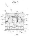
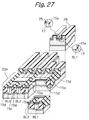
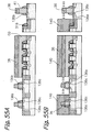
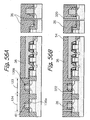
- Tunnel insulation layers or second insulation layers 15a respectively cover one of the side walls 13b and bit line BL1 and the other side wall 13b and bit line BL2.
- the bit lines BL1 and GBL2 bifunction as source/drain regions, as will be described specifically later. In this sense, the bit lines BL1 and BL2 will be sometimes referred to as source/drain regions.
- a control gate CG faces the floating gates FG1 and FG2 via the inter-polycrystalline insulation layers 15b and faces the top surface 13c of the projection 13a via the gate insulation layer 15c.
- the control gate CG may comprise segments facing the floating gates FG1 and FG2 with the inter-polycrystalline insulation layers 15b intervening in between and a segment facing the top surface 13c with the gate insulation layer 15c intervening in between. In such an alternative case, the above segments will be electrically separate from and electrically controlled independently of each other.
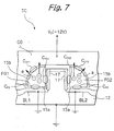
- FIG. 2 shows an equivalent circuit representative of the cell transistor TC and including various capacitance associated therewith.
- the capacitance is represented by a capacitor C CG between the control gate CG and the top 13c of the projection 13c, a capacitor C CF1 (C CF2 ) between the control gate CG and the floating gate FG1 (FG2) facing each other, a capacitor C FG1 (C FG2 ) between the floating ate FG1 (FG2) and the side 13b of the projection 13a facing each other, and a capacitor C FS (C FD ) between the floating gate FG1 (FG2) and the source/drain region BL1 (BL2) facing each other.
- the other select lines SE i-1 , SO i and SO i+1 are caused to go low for thereby turning off all of the transistors whose gates are connected to such select lines.
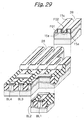
- the sacrifice silicon oxide layer 31 and part of each of the bit lines BL1 through BL4 are selectively etched with the silicon nitride layer 30 serving as a mask. As a result, an about 10 nm deep recess 32 is formed in each of the bit lines BL1 through BL4.
- arsenic ions are implanted in the bit lines BL1 through BL4 via the slots 30a in order to lower the resistance of the bit lines BL1 through BL4.
- Portions 33 where arsenic ions are so implanted constitute high-concentration regions, i.e., n + regions that lower the resistance of the bit lines BL1 through BL4 in the direction of column.
- This implantation is effected with an ion seed of As, acceleration energy of 30 keV, and a dose of 3.0 x 10 15 cm -2 .
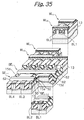
- the illustrative embodiment additionally includes metal wires or third metal wires 306 (see FIG. 37) each extending in the direction of column.
- the third metal wires 306 are connected to the source/drain regions between nearby control gates for thereby lowering the resistance of the source/drains in the direction of column in cooperation with the virtual ground lines.
- the third metal wires each are assigned to a particular bank.
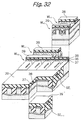
- the device isolation regions STIa should preferably be implemented as STI regions that occupy a minimum of area and therefore reduce the overall size of the semiconductor memory.
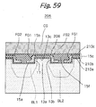
- a BPSG (Boro-Phospho Silicate Glass) layer 36 is formed on the entire surface of the laminate and used to flatten the surface for aluminum wires. More specifically, after the BPSG layer 36 has been heated at high temperature to reduce the irregularity of the surface, the surface of the BPSG layer 36 is flattened by CMP.
- a coupling ratio refers to a ratio C CF1 /(C FG1 + C FS ) or C CF2 /(C FG2 + C FD ) where C CF1 , C CF2 and so forth denote the various capacitors stated earlier with reference to FIG. 2.
- the cell transistor shown in FIG. 1 has a coupling capacitance CR of about 0.37 while the transistor of the illustrative embodiment achieves a coupling ratio of 0.35 or below or around 0.32 for the following reason.
- the floating gates FG1 and FG2 of FIG. 1 each have a generally sectorial shape whose center angle is 90°.
- the floating gates FG1 and FG2 of the illustrative embodiment each have a square shape, so that the contact area with the control gate CG is reduced.
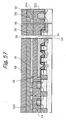
- a plurality of cell transistors are arranged in the direction in which the source/drain regions BL1 and BL2 are positioned side by side. As shown in FIG. 58, An insulation layer 15f is positioned between the floating gate FG1 of one of nearby cell transistors and the floating gate FG2 of the other cell transistor for the following reason.
- the present invention is applicable not only to a semiconductor memory shown and described, but also to any other semiconductor device. While one conductivity type and counter conductivity type are respectively assumed to be P type and N type in the illustrative embodiments, they may, of course, be replaced with each other.
- Drive transistors and select transistors are positioned at different levels from each other, but can be formed at the same time by a single step, obviating the need for an extra step. Also, insulation films for protection are formed on the ends of projections in the direction of column at the same time as LDD side wall insulation layers, further reducing the number of manufacturing steps.
Landscapes
- Semiconductor Memories (AREA)
- Non-Volatile Memory (AREA)
- Metal-Oxide And Bipolar Metal-Oxide Semiconductor Integrated Circuits (AREA)
- Read Only Memory (AREA)
Applications Claiming Priority (4)
| Application Number | Priority Date | Filing Date | Title |
|---|---|---|---|
| JP2002089744 | 2002-03-27 | ||
| JP2002089744 | 2002-03-27 | ||
| JP2003036005A JP4472934B2 (ja) | 2002-03-27 | 2003-02-14 | 半導体装置および半導体メモリ |
| JP2003036005 | 2003-02-14 |
Publications (1)
| Publication Number | Publication Date |
|---|---|
| EP1349215A2 true EP1349215A2 (en) | 2003-10-01 |
Family
ID=27807028
Family Applications (1)
| Application Number | Title | Priority Date | Filing Date |
|---|---|---|---|
| EP03006801A Withdrawn EP1349215A2 (en) | 2002-03-27 | 2003-03-26 | Semiconductor device and semicondutor memory using the same |
Country Status (6)
| Country | Link |
|---|---|
| US (2) | US6984863B2 (enExample) |
| EP (1) | EP1349215A2 (enExample) |
| JP (1) | JP4472934B2 (enExample) |
| KR (1) | KR20030078023A (enExample) |
| CN (1) | CN1447436A (enExample) |
| TW (1) | TW200308079A (enExample) |
Families Citing this family (25)
| Publication number | Priority date | Publication date | Assignee | Title |
|---|---|---|---|---|
| JP2004214495A (ja) * | 2003-01-07 | 2004-07-29 | Innotech Corp | トランジスタとそれを用いた半導体メモリ、および半導体メモリの製造方法 |
| US6914825B2 (en) * | 2003-04-03 | 2005-07-05 | Ememory Technology Inc. | Semiconductor memory device having improved data retention |
| US6936883B2 (en) * | 2003-04-07 | 2005-08-30 | Silicon Storage Technology, Inc. | Bi-directional read/program non-volatile floating gate memory cell and array thereof, and method of formation |
| US6967143B2 (en) * | 2003-04-30 | 2005-11-22 | Freescale Semiconductor, Inc. | Semiconductor fabrication process with asymmetrical conductive spacers |
| US7192876B2 (en) * | 2003-05-22 | 2007-03-20 | Freescale Semiconductor, Inc. | Transistor with independent gate structures |
| WO2004109806A1 (ja) * | 2003-06-04 | 2004-12-16 | Fujitsu Limited | 不揮発性半導体メモリ |
| US7202523B2 (en) * | 2003-11-17 | 2007-04-10 | Micron Technology, Inc. | NROM flash memory devices on ultrathin silicon |
| KR100618819B1 (ko) * | 2004-02-06 | 2006-08-31 | 삼성전자주식회사 | 오버레이 마진이 개선된 반도체 소자 및 그 제조방법 |
| JP4557678B2 (ja) * | 2004-02-13 | 2010-10-06 | イノテック株式会社 | 半導体記憶装置 |
| US7087950B2 (en) * | 2004-04-30 | 2006-08-08 | Infineon Technologies Ag | Flash memory cell, flash memory device and manufacturing method thereof |
| KR101488516B1 (ko) * | 2006-03-21 | 2015-02-02 | 가부시키가이샤 한도오따이 에네루기 켄큐쇼 | 불휘발성 반도체 기억장치 |
| JP5164406B2 (ja) * | 2006-03-21 | 2013-03-21 | 株式会社半導体エネルギー研究所 | 不揮発性半導体記憶装置 |
| JP5164405B2 (ja) * | 2006-03-21 | 2013-03-21 | 株式会社半導体エネルギー研究所 | 不揮発性半導体記憶装置 |
| JP5164404B2 (ja) * | 2006-03-21 | 2013-03-21 | 株式会社半導体エネルギー研究所 | 不揮発性半導体記憶装置 |
| TWI416738B (zh) | 2006-03-21 | 2013-11-21 | Semiconductor Energy Lab | 非揮發性半導體記憶體裝置 |
| EP1837917A1 (en) * | 2006-03-21 | 2007-09-26 | Semiconductor Energy Laboratory Co., Ltd. | Nonvolatile semiconductor memory device |
| JP2007288175A (ja) * | 2006-03-21 | 2007-11-01 | Semiconductor Energy Lab Co Ltd | 不揮発性半導体記憶装置 |
| JP5466815B2 (ja) * | 2006-03-31 | 2014-04-09 | 株式会社半導体エネルギー研究所 | 半導体装置 |
| EP1840947A3 (en) | 2006-03-31 | 2008-08-13 | Semiconductor Energy Laboratory Co., Ltd. | Nonvolatile semiconductor memory device |
| JP5483659B2 (ja) * | 2006-03-31 | 2014-05-07 | 株式会社半導体エネルギー研究所 | 半導体装置 |
| JP2007294911A (ja) * | 2006-03-31 | 2007-11-08 | Semiconductor Energy Lab Co Ltd | 不揮発性半導体記憶装置 |
| US7755132B2 (en) | 2006-08-16 | 2010-07-13 | Sandisk Corporation | Nonvolatile memories with shaped floating gates |
| US7494860B2 (en) * | 2006-08-16 | 2009-02-24 | Sandisk Corporation | Methods of forming nonvolatile memories with L-shaped floating gates |
| JP5270205B2 (ja) | 2008-03-24 | 2013-08-21 | 株式会社Dnpファインケミカル | インクジェット記録用油性緑色インク組成物およびインクジェット記録用油性インクセット |
| KR101096907B1 (ko) * | 2009-10-05 | 2011-12-22 | 주식회사 하이닉스반도체 | 반도체 소자 및 그 형성방법 |
Family Cites Families (9)
| Publication number | Priority date | Publication date | Assignee | Title |
|---|---|---|---|---|
| US5379255A (en) | 1992-12-14 | 1995-01-03 | Texas Instruments Incorporated | Three dimensional famos memory devices and methods of fabricating |
| JP4397491B2 (ja) | 1999-11-30 | 2010-01-13 | 財団法人国際科学振興財団 | 111面方位を表面に有するシリコンを用いた半導体装置およびその形成方法 |
| JP3283872B1 (ja) | 2001-04-12 | 2002-05-20 | イノテック株式会社 | 半導体記憶装置、その製造方法及び半導体記憶装置の駆動方法 |
| JP3249811B1 (ja) | 2000-11-09 | 2002-01-21 | イノテック株式会社 | 半導体記憶装置、その製造方法及び半導体記憶装置の駆動方法 |
| JP3249812B1 (ja) | 2001-05-14 | 2002-01-21 | イノテック株式会社 | 半導体記憶装置及びその製造方法 |
| JP4191975B2 (ja) | 2001-11-01 | 2008-12-03 | イノテック株式会社 | トランジスタとそれを用いた半導体メモリ、およびトランジスタの製造方法 |
| JP2004072060A (ja) | 2001-11-22 | 2004-03-04 | Innotech Corp | トランジスタとそれを用いた半導体メモリ、およびトランジスタの駆動方法 |
| JP2003224215A (ja) | 2001-11-22 | 2003-08-08 | Innotech Corp | トランジスタとそれを用いた半導体メモリ、およびトランジスタの駆動方法 |
| US6861315B1 (en) | 2003-08-14 | 2005-03-01 | Silicon Storage Technology, Inc. | Method of manufacturing an array of bi-directional nonvolatile memory cells |
-
2003
- 2003-02-14 JP JP2003036005A patent/JP4472934B2/ja not_active Expired - Lifetime
- 2003-03-06 TW TW092104783A patent/TW200308079A/zh unknown
- 2003-03-26 EP EP03006801A patent/EP1349215A2/en not_active Withdrawn
- 2003-03-26 KR KR10-2003-0018958A patent/KR20030078023A/ko not_active Withdrawn
- 2003-03-27 US US10/397,377 patent/US6984863B2/en not_active Expired - Fee Related
- 2003-03-27 CN CN03128647A patent/CN1447436A/zh active Pending
-
2005
- 2005-09-28 US US11/236,629 patent/US7221029B2/en not_active Expired - Fee Related
Also Published As
| Publication number | Publication date |
|---|---|
| CN1447436A (zh) | 2003-10-08 |
| TW200308079A (en) | 2003-12-16 |
| US20030183872A1 (en) | 2003-10-02 |
| KR20030078023A (ko) | 2003-10-04 |
| US6984863B2 (en) | 2006-01-10 |
| JP4472934B2 (ja) | 2010-06-02 |
| US20060027857A1 (en) | 2006-02-09 |
| US7221029B2 (en) | 2007-05-22 |
| JP2004006658A (ja) | 2004-01-08 |
Similar Documents
| Publication | Publication Date | Title |
|---|---|---|
| US6984863B2 (en) | Semiconductor decive and semiconductor memory using the same | |
| US7662686B2 (en) | Semiconductor device and a method of manufacturing the same | |
| KR100417451B1 (ko) | 판독전용메모리셀구조를제조하기위한방법 | |
| US6611019B2 (en) | Method and structure for an improved floating gate memory cell | |
| US7221008B2 (en) | Bitline direction shielding to avoid cross coupling between adjacent cells for NAND flash memory | |
| EP2264756A1 (en) | Semiconductor device | |
| US20160329399A1 (en) | Semiconductor device and method for manufacturing semiconductor device | |
| US6610570B2 (en) | Double-bit non-volatile memory structure and corresponding method of manufacture | |
| EP1437774A2 (en) | Transistor storing multiple bits and method of manufacturing semiconductor memory including the same | |
| US7023048B2 (en) | Nonvolatile semiconductor memory devices and the fabrication process of them | |
| US7375387B2 (en) | Method for producing semiconductor memory devices and integrated memory device | |
| KR20040030705A (ko) | 트랜지스터 장치, 트랜지스터 장치를 데이터 메모리로서작동시키는 방법 및 트랜지스터 장치의 제조 방법 | |
| CN120076325B (zh) | 110nm以下的嵌入式闪存及其制备方法 | |
| US20070069275A1 (en) | Bi-directional read/program non-volatile floating gate memory array, and method of formation | |
| US6834011B2 (en) | Structure, fabrication method and operating method for flash memory | |
| KR20060043534A (ko) | 트렌치 내에 독립적인 제어 가능한 제어 게이트를 갖는 매립형 비트 라인 불휘발성 부동 게이트 메모리 셀, 및 그 어레이, 및 형성 방법 | |
| JP2003031700A (ja) | 不揮発性半導体記憶装置、その動作方法および製造方法 |
Legal Events
| Date | Code | Title | Description |
|---|---|---|---|
| PUAI | Public reference made under article 153(3) epc to a published international application that has entered the european phase |
Free format text: ORIGINAL CODE: 0009012 |
|
| AK | Designated contracting states |
Kind code of ref document: A2 Designated state(s): AT BE BG CH CY CZ DE DK EE ES FI FR GB GR HU IE IT LI LU MC NL PT RO SE SI SK TR |
|
| AX | Request for extension of the european patent |
Extension state: AL LT LV MK |
|
| STAA | Information on the status of an ep patent application or granted ep patent |
Free format text: STATUS: THE APPLICATION IS DEEMED TO BE WITHDRAWN |
|
| 18D | Application deemed to be withdrawn |
Effective date: 20071002 |