EP1291906B1 - Fabrication method for a semiconductor device - Google Patents
Fabrication method for a semiconductor device Download PDFInfo
- Publication number
- EP1291906B1 EP1291906B1 EP01915802A EP01915802A EP1291906B1 EP 1291906 B1 EP1291906 B1 EP 1291906B1 EP 01915802 A EP01915802 A EP 01915802A EP 01915802 A EP01915802 A EP 01915802A EP 1291906 B1 EP1291906 B1 EP 1291906B1
- Authority
- EP
- European Patent Office
- Prior art keywords
- forming
- wiring
- semiconductor device
- layer
- etching
- Prior art date
- Legal status (The legal status is an assumption and is not a legal conclusion. Google has not performed a legal analysis and makes no representation as to the accuracy of the status listed.)
- Expired - Lifetime
Links
- 239000004065 semiconductor Substances 0.000 title claims abstract description 70
- 238000004519 manufacturing process Methods 0.000 title claims abstract description 18
- 238000000034 method Methods 0.000 title abstract description 20
- 238000005530 etching Methods 0.000 claims abstract description 62
- 239000002184 metal Substances 0.000 claims abstract description 53
- 229910052751 metal Inorganic materials 0.000 claims abstract description 53
- 239000011888 foil Substances 0.000 claims abstract description 44
- 238000010030 laminating Methods 0.000 claims abstract description 10
- RYGMFSIKBFXOCR-UHFFFAOYSA-N Copper Chemical compound [Cu] RYGMFSIKBFXOCR-UHFFFAOYSA-N 0.000 claims description 45
- PXHVJJICTQNCMI-UHFFFAOYSA-N Nickel Chemical compound [Ni] PXHVJJICTQNCMI-UHFFFAOYSA-N 0.000 claims description 41
- 229910052802 copper Inorganic materials 0.000 claims description 26
- 239000010949 copper Substances 0.000 claims description 26
- 239000011889 copper foil Substances 0.000 claims description 19
- 229910052759 nickel Inorganic materials 0.000 claims description 19
- 229910000679 solder Inorganic materials 0.000 claims description 14
- 239000011248 coating agent Substances 0.000 claims description 9
- 238000000576 coating method Methods 0.000 claims description 9
- 238000007747 plating Methods 0.000 claims description 7
- 239000011347 resin Substances 0.000 claims description 5
- 229920005989 resin Polymers 0.000 claims description 5
- 238000005498 polishing Methods 0.000 claims description 4
- 239000004020 conductor Substances 0.000 abstract description 13
- 235000012431 wafers Nutrition 0.000 description 28
- 238000005520 cutting process Methods 0.000 description 9
- 230000018109 developmental process Effects 0.000 description 8
- 238000003475 lamination Methods 0.000 description 8
- 239000003513 alkali Substances 0.000 description 7
- 230000015572 biosynthetic process Effects 0.000 description 4
- 239000010408 film Substances 0.000 description 4
- 239000000463 material Substances 0.000 description 4
- 239000000758 substrate Substances 0.000 description 4
- 230000007261 regionalization Effects 0.000 description 3
- 238000004140 cleaning Methods 0.000 description 2
- 238000004544 sputter deposition Methods 0.000 description 2
- 238000007740 vapor deposition Methods 0.000 description 2
- 239000004642 Polyimide Substances 0.000 description 1
- 230000004888 barrier function Effects 0.000 description 1
- 239000000919 ceramic Substances 0.000 description 1
- 229910052804 chromium Inorganic materials 0.000 description 1
- 229910003460 diamond Inorganic materials 0.000 description 1
- 239000010432 diamond Substances 0.000 description 1
- 238000004070 electrodeposition Methods 0.000 description 1
- 230000008030 elimination Effects 0.000 description 1
- 238000003379 elimination reaction Methods 0.000 description 1
- 238000005538 encapsulation Methods 0.000 description 1
- 230000010354 integration Effects 0.000 description 1
- 229910052750 molybdenum Inorganic materials 0.000 description 1
- 238000004806 packaging method and process Methods 0.000 description 1
- 229920001721 polyimide Polymers 0.000 description 1
- 238000005549 size reduction Methods 0.000 description 1
- 238000005476 soldering Methods 0.000 description 1
- 239000010409 thin film Substances 0.000 description 1
- 229910052721 tungsten Inorganic materials 0.000 description 1
Images


Classifications
-
- H—ELECTRICITY
- H01—ELECTRIC ELEMENTS
- H01L—SEMICONDUCTOR DEVICES NOT COVERED BY CLASS H10
- H01L24/00—Arrangements for connecting or disconnecting semiconductor or solid-state bodies; Methods or apparatus related thereto
- H01L24/01—Means for bonding being attached to, or being formed on, the surface to be connected, e.g. chip-to-package, die-attach, "first-level" interconnects; Manufacturing methods related thereto
- H01L24/10—Bump connectors ; Manufacturing methods related thereto
- H01L24/12—Structure, shape, material or disposition of the bump connectors prior to the connecting process
-
- H—ELECTRICITY
- H01—ELECTRIC ELEMENTS
- H01L—SEMICONDUCTOR DEVICES NOT COVERED BY CLASS H10
- H01L21/00—Processes or apparatus adapted for the manufacture or treatment of semiconductor or solid state devices or of parts thereof
- H01L21/02—Manufacture or treatment of semiconductor devices or of parts thereof
- H01L21/04—Manufacture or treatment of semiconductor devices or of parts thereof the devices having potential barriers, e.g. a PN junction, depletion layer or carrier concentration layer
- H01L21/50—Assembly of semiconductor devices using processes or apparatus not provided for in a single one of the subgroups H01L21/06 - H01L21/326, e.g. sealing of a cap to a base of a container
- H01L21/60—Attaching or detaching leads or other conductive members, to be used for carrying current to or from the device in operation
-
- H—ELECTRICITY
- H01—ELECTRIC ELEMENTS
- H01L—SEMICONDUCTOR DEVICES NOT COVERED BY CLASS H10
- H01L23/00—Details of semiconductor or other solid state devices
- H01L23/28—Encapsulations, e.g. encapsulating layers, coatings, e.g. for protection
- H01L23/31—Encapsulations, e.g. encapsulating layers, coatings, e.g. for protection characterised by the arrangement or shape
- H01L23/3107—Encapsulations, e.g. encapsulating layers, coatings, e.g. for protection characterised by the arrangement or shape the device being completely enclosed
- H01L23/3114—Encapsulations, e.g. encapsulating layers, coatings, e.g. for protection characterised by the arrangement or shape the device being completely enclosed the device being a chip scale package, e.g. CSP
-
- H—ELECTRICITY
- H01—ELECTRIC ELEMENTS
- H01L—SEMICONDUCTOR DEVICES NOT COVERED BY CLASS H10
- H01L24/00—Arrangements for connecting or disconnecting semiconductor or solid-state bodies; Methods or apparatus related thereto
- H01L24/01—Means for bonding being attached to, or being formed on, the surface to be connected, e.g. chip-to-package, die-attach, "first-level" interconnects; Manufacturing methods related thereto
- H01L24/02—Bonding areas ; Manufacturing methods related thereto
-
- H—ELECTRICITY
- H01—ELECTRIC ELEMENTS
- H01L—SEMICONDUCTOR DEVICES NOT COVERED BY CLASS H10
- H01L24/00—Arrangements for connecting or disconnecting semiconductor or solid-state bodies; Methods or apparatus related thereto
- H01L24/01—Means for bonding being attached to, or being formed on, the surface to be connected, e.g. chip-to-package, die-attach, "first-level" interconnects; Manufacturing methods related thereto
- H01L24/10—Bump connectors ; Manufacturing methods related thereto
- H01L24/11—Manufacturing methods
-
- H—ELECTRICITY
- H01—ELECTRIC ELEMENTS
- H01L—SEMICONDUCTOR DEVICES NOT COVERED BY CLASS H10
- H01L24/00—Arrangements for connecting or disconnecting semiconductor or solid-state bodies; Methods or apparatus related thereto
- H01L24/93—Batch processes
- H01L24/94—Batch processes at wafer-level, i.e. with connecting carried out on a wafer comprising a plurality of undiced individual devices
-
- H—ELECTRICITY
- H01—ELECTRIC ELEMENTS
- H01L—SEMICONDUCTOR DEVICES NOT COVERED BY CLASS H10
- H01L2224/00—Indexing scheme for arrangements for connecting or disconnecting semiconductor or solid-state bodies and methods related thereto as covered by H01L24/00
- H01L2224/01—Means for bonding being attached to, or being formed on, the surface to be connected, e.g. chip-to-package, die-attach, "first-level" interconnects; Manufacturing methods related thereto
- H01L2224/02—Bonding areas; Manufacturing methods related thereto
- H01L2224/023—Redistribution layers [RDL] for bonding areas
- H01L2224/0231—Manufacturing methods of the redistribution layers
- H01L2224/02313—Subtractive methods
-
- H—ELECTRICITY
- H01—ELECTRIC ELEMENTS
- H01L—SEMICONDUCTOR DEVICES NOT COVERED BY CLASS H10
- H01L2224/00—Indexing scheme for arrangements for connecting or disconnecting semiconductor or solid-state bodies and methods related thereto as covered by H01L24/00
- H01L2224/01—Means for bonding being attached to, or being formed on, the surface to be connected, e.g. chip-to-package, die-attach, "first-level" interconnects; Manufacturing methods related thereto
- H01L2224/02—Bonding areas; Manufacturing methods related thereto
- H01L2224/023—Redistribution layers [RDL] for bonding areas
- H01L2224/0231—Manufacturing methods of the redistribution layers
- H01L2224/02319—Manufacturing methods of the redistribution layers by using a preform
-
- H—ELECTRICITY
- H01—ELECTRIC ELEMENTS
- H01L—SEMICONDUCTOR DEVICES NOT COVERED BY CLASS H10
- H01L2224/00—Indexing scheme for arrangements for connecting or disconnecting semiconductor or solid-state bodies and methods related thereto as covered by H01L24/00
- H01L2224/01—Means for bonding being attached to, or being formed on, the surface to be connected, e.g. chip-to-package, die-attach, "first-level" interconnects; Manufacturing methods related thereto
- H01L2224/02—Bonding areas; Manufacturing methods related thereto
- H01L2224/023—Redistribution layers [RDL] for bonding areas
- H01L2224/0237—Disposition of the redistribution layers
- H01L2224/02377—Fan-in arrangement
-
- H—ELECTRICITY
- H01—ELECTRIC ELEMENTS
- H01L—SEMICONDUCTOR DEVICES NOT COVERED BY CLASS H10
- H01L2224/00—Indexing scheme for arrangements for connecting or disconnecting semiconductor or solid-state bodies and methods related thereto as covered by H01L24/00
- H01L2224/01—Means for bonding being attached to, or being formed on, the surface to be connected, e.g. chip-to-package, die-attach, "first-level" interconnects; Manufacturing methods related thereto
- H01L2224/02—Bonding areas; Manufacturing methods related thereto
- H01L2224/03—Manufacturing methods
- H01L2224/034—Manufacturing methods by blanket deposition of the material of the bonding area
- H01L2224/0343—Manufacturing methods by blanket deposition of the material of the bonding area in solid form
- H01L2224/03436—Lamination of a preform, e.g. foil, sheet or layer
-
- H—ELECTRICITY
- H01—ELECTRIC ELEMENTS
- H01L—SEMICONDUCTOR DEVICES NOT COVERED BY CLASS H10
- H01L2224/00—Indexing scheme for arrangements for connecting or disconnecting semiconductor or solid-state bodies and methods related thereto as covered by H01L24/00
- H01L2224/01—Means for bonding being attached to, or being formed on, the surface to be connected, e.g. chip-to-package, die-attach, "first-level" interconnects; Manufacturing methods related thereto
- H01L2224/02—Bonding areas; Manufacturing methods related thereto
- H01L2224/03—Manufacturing methods
- H01L2224/036—Manufacturing methods by patterning a pre-deposited material
- H01L2224/0361—Physical or chemical etching
-
- H—ELECTRICITY
- H01—ELECTRIC ELEMENTS
- H01L—SEMICONDUCTOR DEVICES NOT COVERED BY CLASS H10
- H01L2224/00—Indexing scheme for arrangements for connecting or disconnecting semiconductor or solid-state bodies and methods related thereto as covered by H01L24/00
- H01L2224/01—Means for bonding being attached to, or being formed on, the surface to be connected, e.g. chip-to-package, die-attach, "first-level" interconnects; Manufacturing methods related thereto
- H01L2224/02—Bonding areas; Manufacturing methods related thereto
- H01L2224/03—Manufacturing methods
- H01L2224/038—Post-treatment of the bonding area
- H01L2224/0383—Reworking, e.g. shaping
- H01L2224/0384—Reworking, e.g. shaping involving a mechanical process, e.g. planarising the bonding area
-
- H—ELECTRICITY
- H01—ELECTRIC ELEMENTS
- H01L—SEMICONDUCTOR DEVICES NOT COVERED BY CLASS H10
- H01L2224/00—Indexing scheme for arrangements for connecting or disconnecting semiconductor or solid-state bodies and methods related thereto as covered by H01L24/00
- H01L2224/01—Means for bonding being attached to, or being formed on, the surface to be connected, e.g. chip-to-package, die-attach, "first-level" interconnects; Manufacturing methods related thereto
- H01L2224/02—Bonding areas; Manufacturing methods related thereto
- H01L2224/04—Structure, shape, material or disposition of the bonding areas prior to the connecting process
- H01L2224/0401—Bonding areas specifically adapted for bump connectors, e.g. under bump metallisation [UBM]
-
- H—ELECTRICITY
- H01—ELECTRIC ELEMENTS
- H01L—SEMICONDUCTOR DEVICES NOT COVERED BY CLASS H10
- H01L2224/00—Indexing scheme for arrangements for connecting or disconnecting semiconductor or solid-state bodies and methods related thereto as covered by H01L24/00
- H01L2224/01—Means for bonding being attached to, or being formed on, the surface to be connected, e.g. chip-to-package, die-attach, "first-level" interconnects; Manufacturing methods related thereto
- H01L2224/02—Bonding areas; Manufacturing methods related thereto
- H01L2224/04—Structure, shape, material or disposition of the bonding areas prior to the connecting process
- H01L2224/05—Structure, shape, material or disposition of the bonding areas prior to the connecting process of an individual bonding area
- H01L2224/05001—Internal layers
- H01L2224/05005—Structure
- H01L2224/05008—Bonding area integrally formed with a redistribution layer on the semiconductor or solid-state body, e.g.
-
- H—ELECTRICITY
- H01—ELECTRIC ELEMENTS
- H01L—SEMICONDUCTOR DEVICES NOT COVERED BY CLASS H10
- H01L2224/00—Indexing scheme for arrangements for connecting or disconnecting semiconductor or solid-state bodies and methods related thereto as covered by H01L24/00
- H01L2224/01—Means for bonding being attached to, or being formed on, the surface to be connected, e.g. chip-to-package, die-attach, "first-level" interconnects; Manufacturing methods related thereto
- H01L2224/02—Bonding areas; Manufacturing methods related thereto
- H01L2224/04—Structure, shape, material or disposition of the bonding areas prior to the connecting process
- H01L2224/05—Structure, shape, material or disposition of the bonding areas prior to the connecting process of an individual bonding area
- H01L2224/05001—Internal layers
- H01L2224/0502—Disposition
- H01L2224/05024—Disposition the internal layer being disposed on a redistribution layer on the semiconductor or solid-state body
-
- H—ELECTRICITY
- H01—ELECTRIC ELEMENTS
- H01L—SEMICONDUCTOR DEVICES NOT COVERED BY CLASS H10
- H01L2224/00—Indexing scheme for arrangements for connecting or disconnecting semiconductor or solid-state bodies and methods related thereto as covered by H01L24/00
- H01L2224/01—Means for bonding being attached to, or being formed on, the surface to be connected, e.g. chip-to-package, die-attach, "first-level" interconnects; Manufacturing methods related thereto
- H01L2224/02—Bonding areas; Manufacturing methods related thereto
- H01L2224/04—Structure, shape, material or disposition of the bonding areas prior to the connecting process
- H01L2224/05—Structure, shape, material or disposition of the bonding areas prior to the connecting process of an individual bonding area
- H01L2224/05001—Internal layers
- H01L2224/05099—Material
- H01L2224/051—Material with a principal constituent of the material being a metal or a metalloid, e.g. boron [B], silicon [Si], germanium [Ge], arsenic [As], antimony [Sb], tellurium [Te] and polonium [Po], and alloys thereof
- H01L2224/05138—Material with a principal constituent of the material being a metal or a metalloid, e.g. boron [B], silicon [Si], germanium [Ge], arsenic [As], antimony [Sb], tellurium [Te] and polonium [Po], and alloys thereof the principal constituent melting at a temperature of greater than or equal to 950°C and less than 1550°C
- H01L2224/05147—Copper [Cu] as principal constituent
-
- H—ELECTRICITY
- H01—ELECTRIC ELEMENTS
- H01L—SEMICONDUCTOR DEVICES NOT COVERED BY CLASS H10
- H01L2224/00—Indexing scheme for arrangements for connecting or disconnecting semiconductor or solid-state bodies and methods related thereto as covered by H01L24/00
- H01L2224/01—Means for bonding being attached to, or being formed on, the surface to be connected, e.g. chip-to-package, die-attach, "first-level" interconnects; Manufacturing methods related thereto
- H01L2224/02—Bonding areas; Manufacturing methods related thereto
- H01L2224/04—Structure, shape, material or disposition of the bonding areas prior to the connecting process
- H01L2224/05—Structure, shape, material or disposition of the bonding areas prior to the connecting process of an individual bonding area
- H01L2224/05001—Internal layers
- H01L2224/05099—Material
- H01L2224/051—Material with a principal constituent of the material being a metal or a metalloid, e.g. boron [B], silicon [Si], germanium [Ge], arsenic [As], antimony [Sb], tellurium [Te] and polonium [Po], and alloys thereof
- H01L2224/05138—Material with a principal constituent of the material being a metal or a metalloid, e.g. boron [B], silicon [Si], germanium [Ge], arsenic [As], antimony [Sb], tellurium [Te] and polonium [Po], and alloys thereof the principal constituent melting at a temperature of greater than or equal to 950°C and less than 1550°C
- H01L2224/05155—Nickel [Ni] as principal constituent
-
- H—ELECTRICITY
- H01—ELECTRIC ELEMENTS
- H01L—SEMICONDUCTOR DEVICES NOT COVERED BY CLASS H10
- H01L2224/00—Indexing scheme for arrangements for connecting or disconnecting semiconductor or solid-state bodies and methods related thereto as covered by H01L24/00
- H01L2224/01—Means for bonding being attached to, or being formed on, the surface to be connected, e.g. chip-to-package, die-attach, "first-level" interconnects; Manufacturing methods related thereto
- H01L2224/02—Bonding areas; Manufacturing methods related thereto
- H01L2224/04—Structure, shape, material or disposition of the bonding areas prior to the connecting process
- H01L2224/05—Structure, shape, material or disposition of the bonding areas prior to the connecting process of an individual bonding area
- H01L2224/0554—External layer
- H01L2224/05541—Structure
- H01L2224/05548—Bonding area integrally formed with a redistribution layer on the semiconductor or solid-state body
-
- H—ELECTRICITY
- H01—ELECTRIC ELEMENTS
- H01L—SEMICONDUCTOR DEVICES NOT COVERED BY CLASS H10
- H01L2224/00—Indexing scheme for arrangements for connecting or disconnecting semiconductor or solid-state bodies and methods related thereto as covered by H01L24/00
- H01L2224/01—Means for bonding being attached to, or being formed on, the surface to be connected, e.g. chip-to-package, die-attach, "first-level" interconnects; Manufacturing methods related thereto
- H01L2224/02—Bonding areas; Manufacturing methods related thereto
- H01L2224/04—Structure, shape, material or disposition of the bonding areas prior to the connecting process
- H01L2224/05—Structure, shape, material or disposition of the bonding areas prior to the connecting process of an individual bonding area
- H01L2224/0554—External layer
- H01L2224/0556—Disposition
- H01L2224/05569—Disposition the external layer being disposed on a redistribution layer on the semiconductor or solid-state body
-
- H—ELECTRICITY
- H01—ELECTRIC ELEMENTS
- H01L—SEMICONDUCTOR DEVICES NOT COVERED BY CLASS H10
- H01L2224/00—Indexing scheme for arrangements for connecting or disconnecting semiconductor or solid-state bodies and methods related thereto as covered by H01L24/00
- H01L2224/01—Means for bonding being attached to, or being formed on, the surface to be connected, e.g. chip-to-package, die-attach, "first-level" interconnects; Manufacturing methods related thereto
- H01L2224/02—Bonding areas; Manufacturing methods related thereto
- H01L2224/04—Structure, shape, material or disposition of the bonding areas prior to the connecting process
- H01L2224/05—Structure, shape, material or disposition of the bonding areas prior to the connecting process of an individual bonding area
- H01L2224/0554—External layer
- H01L2224/05599—Material
- H01L2224/056—Material with a principal constituent of the material being a metal or a metalloid, e.g. boron [B], silicon [Si], germanium [Ge], arsenic [As], antimony [Sb], tellurium [Te] and polonium [Po], and alloys thereof
- H01L2224/05638—Material with a principal constituent of the material being a metal or a metalloid, e.g. boron [B], silicon [Si], germanium [Ge], arsenic [As], antimony [Sb], tellurium [Te] and polonium [Po], and alloys thereof the principal constituent melting at a temperature of greater than or equal to 950°C and less than 1550°C
- H01L2224/05647—Copper [Cu] as principal constituent
-
- H—ELECTRICITY
- H01—ELECTRIC ELEMENTS
- H01L—SEMICONDUCTOR DEVICES NOT COVERED BY CLASS H10
- H01L2224/00—Indexing scheme for arrangements for connecting or disconnecting semiconductor or solid-state bodies and methods related thereto as covered by H01L24/00
- H01L2224/01—Means for bonding being attached to, or being formed on, the surface to be connected, e.g. chip-to-package, die-attach, "first-level" interconnects; Manufacturing methods related thereto
- H01L2224/02—Bonding areas; Manufacturing methods related thereto
- H01L2224/04—Structure, shape, material or disposition of the bonding areas prior to the connecting process
- H01L2224/05—Structure, shape, material or disposition of the bonding areas prior to the connecting process of an individual bonding area
- H01L2224/0554—External layer
- H01L2224/05599—Material
- H01L2224/056—Material with a principal constituent of the material being a metal or a metalloid, e.g. boron [B], silicon [Si], germanium [Ge], arsenic [As], antimony [Sb], tellurium [Te] and polonium [Po], and alloys thereof
- H01L2224/05638—Material with a principal constituent of the material being a metal or a metalloid, e.g. boron [B], silicon [Si], germanium [Ge], arsenic [As], antimony [Sb], tellurium [Te] and polonium [Po], and alloys thereof the principal constituent melting at a temperature of greater than or equal to 950°C and less than 1550°C
- H01L2224/05655—Nickel [Ni] as principal constituent
-
- H—ELECTRICITY
- H01—ELECTRIC ELEMENTS
- H01L—SEMICONDUCTOR DEVICES NOT COVERED BY CLASS H10
- H01L2224/00—Indexing scheme for arrangements for connecting or disconnecting semiconductor or solid-state bodies and methods related thereto as covered by H01L24/00
- H01L2224/01—Means for bonding being attached to, or being formed on, the surface to be connected, e.g. chip-to-package, die-attach, "first-level" interconnects; Manufacturing methods related thereto
- H01L2224/10—Bump connectors; Manufacturing methods related thereto
- H01L2224/11—Manufacturing methods
- H01L2224/114—Manufacturing methods by blanket deposition of the material of the bump connector
- H01L2224/1143—Manufacturing methods by blanket deposition of the material of the bump connector in solid form
- H01L2224/11436—Lamination of a preform, e.g. foil, sheet or layer
-
- H—ELECTRICITY
- H01—ELECTRIC ELEMENTS
- H01L—SEMICONDUCTOR DEVICES NOT COVERED BY CLASS H10
- H01L2224/00—Indexing scheme for arrangements for connecting or disconnecting semiconductor or solid-state bodies and methods related thereto as covered by H01L24/00
- H01L2224/01—Means for bonding being attached to, or being formed on, the surface to be connected, e.g. chip-to-package, die-attach, "first-level" interconnects; Manufacturing methods related thereto
- H01L2224/10—Bump connectors; Manufacturing methods related thereto
- H01L2224/11—Manufacturing methods
- H01L2224/116—Manufacturing methods by patterning a pre-deposited material
- H01L2224/1161—Physical or chemical etching
-
- H—ELECTRICITY
- H01—ELECTRIC ELEMENTS
- H01L—SEMICONDUCTOR DEVICES NOT COVERED BY CLASS H10
- H01L2224/00—Indexing scheme for arrangements for connecting or disconnecting semiconductor or solid-state bodies and methods related thereto as covered by H01L24/00
- H01L2224/01—Means for bonding being attached to, or being formed on, the surface to be connected, e.g. chip-to-package, die-attach, "first-level" interconnects; Manufacturing methods related thereto
- H01L2224/10—Bump connectors; Manufacturing methods related thereto
- H01L2224/12—Structure, shape, material or disposition of the bump connectors prior to the connecting process
- H01L2224/13—Structure, shape, material or disposition of the bump connectors prior to the connecting process of an individual bump connector
- H01L2224/13001—Core members of the bump connector
- H01L2224/1302—Disposition
- H01L2224/13024—Disposition the bump connector being disposed on a redistribution layer on the semiconductor or solid-state body
-
- H—ELECTRICITY
- H01—ELECTRIC ELEMENTS
- H01L—SEMICONDUCTOR DEVICES NOT COVERED BY CLASS H10
- H01L2224/00—Indexing scheme for arrangements for connecting or disconnecting semiconductor or solid-state bodies and methods related thereto as covered by H01L24/00
- H01L2224/01—Means for bonding being attached to, or being formed on, the surface to be connected, e.g. chip-to-package, die-attach, "first-level" interconnects; Manufacturing methods related thereto
- H01L2224/10—Bump connectors; Manufacturing methods related thereto
- H01L2224/12—Structure, shape, material or disposition of the bump connectors prior to the connecting process
- H01L2224/13—Structure, shape, material or disposition of the bump connectors prior to the connecting process of an individual bump connector
- H01L2224/13001—Core members of the bump connector
- H01L2224/13099—Material
- H01L2224/131—Material with a principal constituent of the material being a metal or a metalloid, e.g. boron [B], silicon [Si], germanium [Ge], arsenic [As], antimony [Sb], tellurium [Te] and polonium [Po], and alloys thereof
- H01L2224/13138—Material with a principal constituent of the material being a metal or a metalloid, e.g. boron [B], silicon [Si], germanium [Ge], arsenic [As], antimony [Sb], tellurium [Te] and polonium [Po], and alloys thereof the principal constituent melting at a temperature of greater than or equal to 950°C and less than 1550°C
- H01L2224/13147—Copper [Cu] as principal constituent
-
- H—ELECTRICITY
- H01—ELECTRIC ELEMENTS
- H01L—SEMICONDUCTOR DEVICES NOT COVERED BY CLASS H10
- H01L2224/00—Indexing scheme for arrangements for connecting or disconnecting semiconductor or solid-state bodies and methods related thereto as covered by H01L24/00
- H01L2224/01—Means for bonding being attached to, or being formed on, the surface to be connected, e.g. chip-to-package, die-attach, "first-level" interconnects; Manufacturing methods related thereto
- H01L2224/10—Bump connectors; Manufacturing methods related thereto
- H01L2224/15—Structure, shape, material or disposition of the bump connectors after the connecting process
- H01L2224/16—Structure, shape, material or disposition of the bump connectors after the connecting process of an individual bump connector
-
- H—ELECTRICITY
- H01—ELECTRIC ELEMENTS
- H01L—SEMICONDUCTOR DEVICES NOT COVERED BY CLASS H10
- H01L2224/00—Indexing scheme for arrangements for connecting or disconnecting semiconductor or solid-state bodies and methods related thereto as covered by H01L24/00
- H01L2224/01—Means for bonding being attached to, or being formed on, the surface to be connected, e.g. chip-to-package, die-attach, "first-level" interconnects; Manufacturing methods related thereto
- H01L2224/26—Layer connectors, e.g. plate connectors, solder or adhesive layers; Manufacturing methods related thereto
- H01L2224/27—Manufacturing methods
- H01L2224/274—Manufacturing methods by blanket deposition of the material of the layer connector
-
- H—ELECTRICITY
- H01—ELECTRIC ELEMENTS
- H01L—SEMICONDUCTOR DEVICES NOT COVERED BY CLASS H10
- H01L2224/00—Indexing scheme for arrangements for connecting or disconnecting semiconductor or solid-state bodies and methods related thereto as covered by H01L24/00
- H01L2224/93—Batch processes
- H01L2224/94—Batch processes at wafer-level, i.e. with connecting carried out on a wafer comprising a plurality of undiced individual devices
-
- H—ELECTRICITY
- H01—ELECTRIC ELEMENTS
- H01L—SEMICONDUCTOR DEVICES NOT COVERED BY CLASS H10
- H01L24/00—Arrangements for connecting or disconnecting semiconductor or solid-state bodies; Methods or apparatus related thereto
- H01L24/01—Means for bonding being attached to, or being formed on, the surface to be connected, e.g. chip-to-package, die-attach, "first-level" interconnects; Manufacturing methods related thereto
- H01L24/02—Bonding areas ; Manufacturing methods related thereto
- H01L24/03—Manufacturing methods
-
- H—ELECTRICITY
- H01—ELECTRIC ELEMENTS
- H01L—SEMICONDUCTOR DEVICES NOT COVERED BY CLASS H10
- H01L24/00—Arrangements for connecting or disconnecting semiconductor or solid-state bodies; Methods or apparatus related thereto
- H01L24/01—Means for bonding being attached to, or being formed on, the surface to be connected, e.g. chip-to-package, die-attach, "first-level" interconnects; Manufacturing methods related thereto
- H01L24/02—Bonding areas ; Manufacturing methods related thereto
- H01L24/04—Structure, shape, material or disposition of the bonding areas prior to the connecting process
- H01L24/05—Structure, shape, material or disposition of the bonding areas prior to the connecting process of an individual bonding area
-
- H—ELECTRICITY
- H01—ELECTRIC ELEMENTS
- H01L—SEMICONDUCTOR DEVICES NOT COVERED BY CLASS H10
- H01L24/00—Arrangements for connecting or disconnecting semiconductor or solid-state bodies; Methods or apparatus related thereto
- H01L24/01—Means for bonding being attached to, or being formed on, the surface to be connected, e.g. chip-to-package, die-attach, "first-level" interconnects; Manufacturing methods related thereto
- H01L24/10—Bump connectors ; Manufacturing methods related thereto
- H01L24/12—Structure, shape, material or disposition of the bump connectors prior to the connecting process
- H01L24/13—Structure, shape, material or disposition of the bump connectors prior to the connecting process of an individual bump connector
-
- H—ELECTRICITY
- H01—ELECTRIC ELEMENTS
- H01L—SEMICONDUCTOR DEVICES NOT COVERED BY CLASS H10
- H01L2924/00—Indexing scheme for arrangements or methods for connecting or disconnecting semiconductor or solid-state bodies as covered by H01L24/00
- H01L2924/0001—Technical content checked by a classifier
-
- H—ELECTRICITY
- H01—ELECTRIC ELEMENTS
- H01L—SEMICONDUCTOR DEVICES NOT COVERED BY CLASS H10
- H01L2924/00—Indexing scheme for arrangements or methods for connecting or disconnecting semiconductor or solid-state bodies as covered by H01L24/00
- H01L2924/01—Chemical elements
- H01L2924/01004—Beryllium [Be]
-
- H—ELECTRICITY
- H01—ELECTRIC ELEMENTS
- H01L—SEMICONDUCTOR DEVICES NOT COVERED BY CLASS H10
- H01L2924/00—Indexing scheme for arrangements or methods for connecting or disconnecting semiconductor or solid-state bodies as covered by H01L24/00
- H01L2924/01—Chemical elements
- H01L2924/01006—Carbon [C]
-
- H—ELECTRICITY
- H01—ELECTRIC ELEMENTS
- H01L—SEMICONDUCTOR DEVICES NOT COVERED BY CLASS H10
- H01L2924/00—Indexing scheme for arrangements or methods for connecting or disconnecting semiconductor or solid-state bodies as covered by H01L24/00
- H01L2924/01—Chemical elements
- H01L2924/01013—Aluminum [Al]
-
- H—ELECTRICITY
- H01—ELECTRIC ELEMENTS
- H01L—SEMICONDUCTOR DEVICES NOT COVERED BY CLASS H10
- H01L2924/00—Indexing scheme for arrangements or methods for connecting or disconnecting semiconductor or solid-state bodies as covered by H01L24/00
- H01L2924/01—Chemical elements
- H01L2924/01024—Chromium [Cr]
-
- H—ELECTRICITY
- H01—ELECTRIC ELEMENTS
- H01L—SEMICONDUCTOR DEVICES NOT COVERED BY CLASS H10
- H01L2924/00—Indexing scheme for arrangements or methods for connecting or disconnecting semiconductor or solid-state bodies as covered by H01L24/00
- H01L2924/01—Chemical elements
- H01L2924/01027—Cobalt [Co]
-
- H—ELECTRICITY
- H01—ELECTRIC ELEMENTS
- H01L—SEMICONDUCTOR DEVICES NOT COVERED BY CLASS H10
- H01L2924/00—Indexing scheme for arrangements or methods for connecting or disconnecting semiconductor or solid-state bodies as covered by H01L24/00
- H01L2924/01—Chemical elements
- H01L2924/01029—Copper [Cu]
-
- H—ELECTRICITY
- H01—ELECTRIC ELEMENTS
- H01L—SEMICONDUCTOR DEVICES NOT COVERED BY CLASS H10
- H01L2924/00—Indexing scheme for arrangements or methods for connecting or disconnecting semiconductor or solid-state bodies as covered by H01L24/00
- H01L2924/01—Chemical elements
- H01L2924/01033—Arsenic [As]
-
- H—ELECTRICITY
- H01—ELECTRIC ELEMENTS
- H01L—SEMICONDUCTOR DEVICES NOT COVERED BY CLASS H10
- H01L2924/00—Indexing scheme for arrangements or methods for connecting or disconnecting semiconductor or solid-state bodies as covered by H01L24/00
- H01L2924/01—Chemical elements
- H01L2924/01042—Molybdenum [Mo]
-
- H—ELECTRICITY
- H01—ELECTRIC ELEMENTS
- H01L—SEMICONDUCTOR DEVICES NOT COVERED BY CLASS H10
- H01L2924/00—Indexing scheme for arrangements or methods for connecting or disconnecting semiconductor or solid-state bodies as covered by H01L24/00
- H01L2924/01—Chemical elements
- H01L2924/01074—Tungsten [W]
-
- H—ELECTRICITY
- H01—ELECTRIC ELEMENTS
- H01L—SEMICONDUCTOR DEVICES NOT COVERED BY CLASS H10
- H01L2924/00—Indexing scheme for arrangements or methods for connecting or disconnecting semiconductor or solid-state bodies as covered by H01L24/00
- H01L2924/01—Chemical elements
- H01L2924/01075—Rhenium [Re]
-
- H—ELECTRICITY
- H01—ELECTRIC ELEMENTS
- H01L—SEMICONDUCTOR DEVICES NOT COVERED BY CLASS H10
- H01L2924/00—Indexing scheme for arrangements or methods for connecting or disconnecting semiconductor or solid-state bodies as covered by H01L24/00
- H01L2924/01—Chemical elements
- H01L2924/01078—Platinum [Pt]
-
- H—ELECTRICITY
- H01—ELECTRIC ELEMENTS
- H01L—SEMICONDUCTOR DEVICES NOT COVERED BY CLASS H10
- H01L2924/00—Indexing scheme for arrangements or methods for connecting or disconnecting semiconductor or solid-state bodies as covered by H01L24/00
- H01L2924/01—Chemical elements
- H01L2924/01082—Lead [Pb]
-
- H—ELECTRICITY
- H01—ELECTRIC ELEMENTS
- H01L—SEMICONDUCTOR DEVICES NOT COVERED BY CLASS H10
- H01L2924/00—Indexing scheme for arrangements or methods for connecting or disconnecting semiconductor or solid-state bodies as covered by H01L24/00
- H01L2924/013—Alloys
- H01L2924/014—Solder alloys
-
- H—ELECTRICITY
- H01—ELECTRIC ELEMENTS
- H01L—SEMICONDUCTOR DEVICES NOT COVERED BY CLASS H10
- H01L2924/00—Indexing scheme for arrangements or methods for connecting or disconnecting semiconductor or solid-state bodies as covered by H01L24/00
- H01L2924/10—Details of semiconductor or other solid state devices to be connected
- H01L2924/11—Device type
- H01L2924/12—Passive devices, e.g. 2 terminal devices
- H01L2924/1204—Optical Diode
- H01L2924/12042—LASER
-
- H—ELECTRICITY
- H01—ELECTRIC ELEMENTS
- H01L—SEMICONDUCTOR DEVICES NOT COVERED BY CLASS H10
- H01L2924/00—Indexing scheme for arrangements or methods for connecting or disconnecting semiconductor or solid-state bodies as covered by H01L24/00
- H01L2924/10—Details of semiconductor or other solid state devices to be connected
- H01L2924/11—Device type
- H01L2924/14—Integrated circuits
Definitions
- This invention concerns a chip-size semiconductor device formed with conductor wirings for re-arranging electrodes on an IC chip and it, particularly, relates to a fabrication method capable of collective processing at the wafers.
- JP-A-11-121507 proposes a method of packaging in a state of wafer and fabricating a chip-size package.
- bumps for connecting an IC package with the outside are formed at electrode positions in IC.
- the pitch for arranging electrodes of the chip has been narrowed more and more and it is necessary to re-arrange the electrodes on the IC chip to expand the electrode pitch for facilitating subsequent mounting.
- This invention intends to solve the foregoing problems in the prior art and provide a method of fabricating a chip-size package in which the electrode pitch is extended by forming conductor wirings on the side of the electrode forming surface of a semiconductor element efficiently and at a reduced cost and, particularly, to provide a method capable of forming wirings and bumps easily.
- the present inventors have found that the foregoing object can be solved by laminating a wiring-forming metal foil on the side of forming electrodes of a semiconductor wafer formed at the surface thereof with circuit elements by using a bonding technique between a metal foil and ceramics previously filed by the present inventors (refer to International Publication No. WO99/58470 ), and then etching the metal foil to form wirings and dividing the same into individual elements.
- bumps can be formed by laminating a wiring-forming multi-layered metal foil to a semiconductor wafer formed at the surface thereof with circuit elements on the side of the electrode forming surface and by merely etching the wirings having bumps thereon.
- the method of fabricating a semiconductor device includes a step of laminating a wiring-forming multi-layer metal foil comprising a bump-forming layer, an etching stopper layer and a wiring-forming layer to a semiconductor wafer formed at the surface thereof with circuit elements on the electrode forming surface side, a step of forming a bump-forming resist wiring pattern on the bump-forming layer, a step of selectively etching the bump-forming layer down to the etching stopper layer, a step of removing the exposed portion of the etching stopper layer, a step of forming a wiring-forming resist wiring pattern, a step of forming wirings by etching of the wiring-forming layer, a step of removing the wiring-forming resist, and a step of dividing into individual elements.
- the wiring-forming multi-layered metal foil is a metal laminate comprising the three layers of a bump forming copper or solder foil layer, an etching stopper layer of nickel and a wiring forming copper foil layer.
- the thickness of the bump-forming copper or soldering foil is 10 to 100 ⁇ m.
- the etching stopper layer nickel is preferably formed by nickel plating of 0.5 to 3 ⁇ m thickness or is a nickel foil clad of 1 to 10 ⁇ m thickness.
- the thickness of the wiring-forming copper foil is 1 to 100 ⁇ m.
- the semiconductor wafer formed at the surface thereof with circuit elements is preferably a semiconductor wafer formed at the surface thereof with a thin metal film.
- Preferably method of fabricating the semiconductor device according to this invention includes a step of coating an insulative resin and polishing the surface thereof, and a step of forming solder bumps between the step of removing the wiring-forming resist and the step of dividing into individual elements.
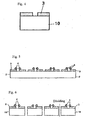
- Fig. 1 is a view showing an example of a circuit forming step for a first embodiment and a second embodiment outside this invention (step of laminating a wiring copper foil on a semiconductor wafer).
- Fig. 2 is a view showing an example of a circuit forming step in a first embodiment and a second embodiment outside this invention (step of forming conductor wirings on the wiring copper foil).
- Fig. 3 is a view showing an example of a circuit forming step in the first embodiment outside this invention (step of cutting into individual elements).
- Fig. 4 is a view showing an example of a circuit forming step in the first embodiment outside this invention (element after cutting).
- Fig. 1 is a view showing an example of a circuit forming step for a first embodiment and a second embodiment outside this invention (step of laminating a wiring copper foil on a semiconductor wafer).
- Fig. 2 is a view showing an example of a circuit forming step in a first embodiment and a second embodiment outside this invention (step of forming
- FIG. 5 is a view showing an example of a circuit forming step in the second embodiment outside this invention (step of forming solder bumps on wiring copper foil).
- Fig. 6 is a view showing an example of a circuit forming step in the second embodiment outside this invention (step of cutting into individual elements).
- Fig. 7 is a view showing an example of a circuit forming step in the second embodiment outside this invention (element after cutting).
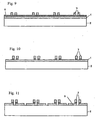
- Fig. 8 is a view showing an example of a circuit forming step in a first embodiment according to this invention (step of laminating a wiring copper foil on a semiconductor wafer).
- Fig. 9 is a view showing an example of a circuit forming step in the first embodiment according to this invention (forming bumps).
- FIG. 10 is a view showing an example of a circuit forming step in the first embodiment according to this invention (selective etching of etching stopper layer nickel).
- Fig. 11 is a view showing an example of a circuit forming step in the first embodiment according to this invention (selective etching of wiring-forming copper foil).
- Fig. 12 is a view showing an example of a circuit forming step in the first embodiment according to this invention (step of cutting into individual elements) .
- Fig. 13 is a view showing an example of a circuit forming step in the first embodiment according to this invention (element after cutting).
- Fig. 14 is a view showing a step of coating an insulative resin and surface polishing in a further embodiment according to this invention.
- Fig. 15 is a view showing a step of forming solder bumps in the further embodiment according to this invention.
- Fig. 16 is a view showing a step of cutting into individual elements in the further embodiment according to this invention.
- Fig. 17 is a view showing an element after cutting in the further embodiment according to this invention.
- Fig. 18 is a front elevational view of an element after cutting in the first or further embodiment according to this invention.
- the first embodiment concerns a semiconductor device comprising a semiconductor wafer formed at the surface thereof with circuit elements, and conductor wirings on the semiconductor element formed by etching a wiring-forming metal foil.
- a semiconductor wafer or the like used ordinarily can be used and, as the wiring-forming metal foil, a foil preferably formed of copper with a thickness of 1 to 100 ⁇ mcan be used.
- the conductor wirings can be formed appropriately into a desired shape.
- the semiconductor device in the first embodiment can be fabricated by a method of fabricating a semiconductor device including a step of laminating a wiring-forming metal foil to a semiconductor wafer formed at the surface thereof with circuit elements on the electrode-forming surface side, a step of forming a resist wiring pattern on the metal foil, a step of etching the metal foil and a step of dividing into individual elements.
- the substrate those used ordinarily such as a semiconductor wafer formed at the surface thereof with circuit elements can be used.
- the wiring-forming metal foil a foil preferably formed of copper and of 1 to 100 ⁇ m thickness can be used as described above
- a thin metal film can be provided on the semiconductor wafer formed at the surface thereof with circuit elements by using a sputtering method, a vapor deposition method or the like after surface cleaning. This can facilitate lamination of the metal foil on the semiconductor wafer.
- the metal forming the thin film Cr, Mo, W or the like is used as a barrier metal in a case where the chip electrode of the semiconductor is Al, but the subsequent removal by etching is difficult. Then, with a view point for the ease of etching elimination, use of nickel is preferred.
- Lamination of the wiring-forming metal foil to the semiconductor wafer can be conducted by using the technique described in International Publication No. WO99/58470 previously filed by the present inventors ( Fig. 1 ).
- a resist is coated on the wiring forming metal foil and then exposure and development are conducted to form a resist wiring pattern.
- the resist wiring pattern is formed preferably such that it can be easily divided subsequently into individual elements and it can adopt, for example, a method of not coating the resist to portions for the division.
- a series of procedures such as resist coating, exposure and development can be conducted based on the ordinary method.
- the wiring-forming metal foil is etched.
- the metal foil is copper
- a commercially available alkali type copper etching solution can be used as the etching solution.
- the second embodiment concerns a semiconductor device comprising a semiconductor element, conductor wirings on the semiconductor element formed by etching a wire-forming metal foil and solder bumps.
- the semiconductor, the wiring-forming metal foil and the conductor wirings are identical with those described for the first embodiment.
- the semiconductor device described above can be fabricated by a method of fabricating a semiconductor device including a step of laminating a wiring-forming metal foil to a semiconductor wafer formed at the surface thereof with circuit elements on the electrode forming surface side, a step of forming a resist wiring pattern on the metal foil, a step of etching the metal foil, a step of forming solder bumps and a step of dividing into individual elements.
- a semiconductor wafer formed at the surface thereof with circuit elements can be used usually and, depending on the case, a thin metal film can be provided after surface cleaning of the semiconductor wafer or the like. Further, lamination of the wiring-forming metal foil to the semiconductor wafer can be conducted in the same manner as in the first embodiment of this invention, by using the technique described in International Publication No. WO99/58470 previously filed by the present inventors ( Fig. 1 ).
- a resist is coated on the wiring-forming metal foil and then exposure and development are conducted to form a resist wiring pattern and, successively, the wiring-forming metal foil is etched and then the resist is removed to form wirings ( Fig. 2 ).
- the resist wiring pattern is preferably applied so as to be divided easily into individual elements subsequently like the first embodiment.
- solder bumps are successively formed ( Fig. 5 ).
- the solver bumps are formed at the positions for re-arranging electrodes.
- the first embodiment of this invention concerns forming a semiconductor device comprising a semiconductor element, and conductor wirings having bumps on the semiconductor element formed by etching the wiring-forming multi-layered metal foil.
- the semiconductor device, the wiring-forming metal foil and the conductor wirings are identical with those described for the first embodiment and the second embodiment outside this invention.
- the thickness of the conductor wirings is 1 to 100 ⁇ m as described above, and for the etching stopper layer, nickel plating of 0. 5 to 3 ⁇ m thickness, preferably, 1 to 2 ⁇ m thickness, or nickel foil clad of 1 to 10 ⁇ m thickness, preferably, 2 to 5 ⁇ m thickness can be used.
- the thickness of the bump is 10 to 100 ⁇ m, preferably, 10 to 50 ⁇ m
- the semiconductor device can be fabricated by a method of fabricating a semiconductor device including a step of laminating a wiring-forming multi-layered metal foil comprising a bump-forming layer, an etching stopper layer and a wiring-forming layer to a semiconductor wafer formed at the surface thereof with circuit elements on the electrode forming surface side, a step of forming a bump-forming resist wiring pattern on the bump-forming layer, a step of selectively etching the bump-forming layer down to the etching stopper layer, a step of removing the exposed portions of the etching stopper layer, a step of forming a wiring-forming resist wiring pattern, a step of forming wirings by etching of the wiring forming layer, a step of removing the wiring-forming resist, and a step of dividing into individual elements.
- a wiring-forming metal laminate is laminated to the semiconductor wafer formed at the surface thereof with circuit elements on the electrode forming surface side ( Fig. 8 ).
- a metal laminate comprising, for example, a bump-forming copper or solder foil (10 to 100 ⁇ m thickness)/etching stopper layer nickel (0.5 to 3 ⁇ m thickness in a case of plating and 1 to 10 ⁇ m thickness in a case of foil)/wiring copper foil (1 to 100 ⁇ m) is used.
- Lamination can be conducted in the same manner as described for the portion of the first embodiment and the second embodiment outside of this invention.
- resist is coated on the metal laminate and then exposure and development are conducted to form a bump-forming resist pattern.
- the bump forming layer in the metal laminate is selectively etched ( Fig. 9 ).
- etching is conducted by using a selective copper etching solution such a commercially available alkali type copper etching solution to form bumps.
- the etching stopper layer is removed.
- the etching stopper layer is nickel plating or foil
- a commercially available nickel removing solution for example, N-950, manufactured by Mertex Co.
- N-950 manufactured by Mertex Co.
- a wiring-forming resist wiring pattern is formed.
- the resist wiring pattern is preferably applied so as to indicate the boundary between each of element regions corresponding to the division into individual element regions to be described later, which is identical with that for the first embodiment and the second embodiment outside of this invention.
- the wiring layer is etched.
- the wiring layer is copper
- a commercially available alkali type copper etching solution or the like can be used.
- the resist is removed ( Fig. 11 ).
- a semiconductor wafer 1 formed at the surface thereof with circuit elements and a wiring-forming copper foil (15 ⁇ m thickness) 2 laminated by the method disclosed in International Publication WO99/58470 were used as a substrate ( Fig. 1 ).
- a thin metal film (nickel) was provided on the semiconductor wafer by using, for example, a sputtering method or a vapor deposition method.
- a semiconductor wafer 1 formed at the surface thereof with circuit elements and a wiring-forming copper foil (15 ⁇ m thickness) 2 laminated in the same manner as in Example 1 were used as a substrate ( Fig. 1 ).
- Solder bumps 4 were formed on wirings at the positions for re-arranging electrodes ( Fig. 5 ).
- a metal laminate comprising bump forming copper foil (35 ⁇ m thickness) 5/etching stopper layer of nickel (plating thickness of 1 ⁇ m) 6/wiring-forming copper foil (15 ⁇ m) 1 was laminated to a semiconductor wafer formed at the surface thereof with circuit elements (identical with that used in Example 1. ( Fig. 8 ).
- Copper was selectively etched by using a commercially available copper etching solution such as an alkali type copper etching solution to form bumps 7 ( Fig. 9 ).
- the etching stopper layer of nickel 6 was removed by using a commercially available nickel removing solution (N-950, manufactured by Mertex Co.) ( Fig. 10 )
- a metal laminate comprising bump forming copper foil (35 ⁇ m thickness) 5/etching stopper layer of nickel (plating thickness 1 ⁇ m) 6/wiring-forming copper foil (15 ⁇ m 1 was laminated to a semiconductor wafer formed at the surface thereof with circuit elements (identical with that used in Example 1 ( Fig. 8 ).
- Copper was selectively etched by using a commercially available copper etching solution such as an alkali type copper etching solution to form bumps 7 ( Fig. 9 ).
- the etching stopper layer of nickel 6 was removed by using a commercially available nickel removing solution (N-950, manufactured by Mertex Co.) ( Fig. 10 )
- An insulative resin such as a polyimide is coated entirely on the semiconductor wafer to apply resin encapsulation. Subsequently, polishing is conducted so as to expose copper bumps to the surface (Fig. 14).
- Solder bumps are formed by using a printing method or the like (Fig. 15)
- a chip-size package in which an electrode pitch is expanded by forming conductor wirings to a semiconductor on the electrode forming surface side can be fabricated efficiently and at a reduced cost. Particularly, wirings and bumps can be formed easily.
- the wiring forming method according to this invention is useful in the field of semiconductors.
Landscapes
- Engineering & Computer Science (AREA)
- Microelectronics & Electronic Packaging (AREA)
- Computer Hardware Design (AREA)
- Power Engineering (AREA)
- Manufacturing & Machinery (AREA)
- Physics & Mathematics (AREA)
- Condensed Matter Physics & Semiconductors (AREA)
- General Physics & Mathematics (AREA)
- Internal Circuitry In Semiconductor Integrated Circuit Devices (AREA)
- Lead Frames For Integrated Circuits (AREA)
- Wire Bonding (AREA)
Applications Claiming Priority (3)
| Application Number | Priority Date | Filing Date | Title |
|---|---|---|---|
| JP2000118227 | 2000-04-19 | ||
| JP2000118227A JP2001308095A (ja) | 2000-04-19 | 2000-04-19 | 半導体装置およびその製造方法 |
| PCT/JP2001/002437 WO2001080299A1 (fr) | 2000-04-19 | 2001-03-27 | Dispositif semi-conducteur et son procede de fabrication |
Publications (3)
| Publication Number | Publication Date |
|---|---|
| EP1291906A1 EP1291906A1 (en) | 2003-03-12 |
| EP1291906A4 EP1291906A4 (en) | 2005-08-31 |
| EP1291906B1 true EP1291906B1 (en) | 2009-11-04 |
Family
ID=18629407
Family Applications (1)
| Application Number | Title | Priority Date | Filing Date |
|---|---|---|---|
| EP01915802A Expired - Lifetime EP1291906B1 (en) | 2000-04-19 | 2001-03-27 | Fabrication method for a semiconductor device |
Country Status (9)
| Country | Link |
|---|---|
| US (1) | US7183190B2 (ja) |
| EP (1) | EP1291906B1 (ja) |
| JP (1) | JP2001308095A (ja) |
| KR (1) | KR100746862B1 (ja) |
| CN (1) | CN1194394C (ja) |
| AU (1) | AU2001242793A1 (ja) |
| DE (1) | DE60140362D1 (ja) |
| TW (1) | TW518921B (ja) |
| WO (1) | WO2001080299A1 (ja) |
Families Citing this family (12)
| Publication number | Priority date | Publication date | Assignee | Title |
|---|---|---|---|---|
| US7495179B2 (en) | 2003-10-06 | 2009-02-24 | Tessera, Inc. | Components with posts and pads |
| US8641913B2 (en) | 2003-10-06 | 2014-02-04 | Tessera, Inc. | Fine pitch microcontacts and method for forming thereof |
| US7709968B2 (en) | 2003-12-30 | 2010-05-04 | Tessera, Inc. | Micro pin grid array with pin motion isolation |
| JP4105202B2 (ja) | 2006-09-26 | 2008-06-25 | 新光電気工業株式会社 | 半導体装置の製造方法 |
| EP2637202A3 (en) * | 2007-09-28 | 2014-03-12 | Tessera, Inc. | Flip chip interconnection with etched posts on a microelectronic element joined to etched posts on a substrate by a fusible metal and corresponding manufacturing method |
| JP2009158593A (ja) * | 2007-12-25 | 2009-07-16 | Tessera Interconnect Materials Inc | バンプ構造およびその製造方法 |
| US8330272B2 (en) | 2010-07-08 | 2012-12-11 | Tessera, Inc. | Microelectronic packages with dual or multiple-etched flip-chip connectors |
| US8580607B2 (en) | 2010-07-27 | 2013-11-12 | Tessera, Inc. | Microelectronic packages with nanoparticle joining |
| US8853558B2 (en) | 2010-12-10 | 2014-10-07 | Tessera, Inc. | Interconnect structure |
| US9633971B2 (en) | 2015-07-10 | 2017-04-25 | Invensas Corporation | Structures and methods for low temperature bonding using nanoparticles |
| US10886250B2 (en) | 2015-07-10 | 2021-01-05 | Invensas Corporation | Structures and methods for low temperature bonding using nanoparticles |
| TWI822659B (zh) | 2016-10-27 | 2023-11-21 | 美商艾德亞半導體科技有限責任公司 | 用於低溫接合的結構和方法 |
Family Cites Families (25)
| Publication number | Priority date | Publication date | Assignee | Title |
|---|---|---|---|---|
| US4380114A (en) * | 1979-04-11 | 1983-04-19 | Teccor Electronics, Inc. | Method of making a semiconductor switching device |
| EP0545328B1 (en) * | 1991-11-29 | 1997-03-19 | Hitachi Chemical Co., Ltd. | Printed circuit board manufacturing process |
| US5976912A (en) * | 1994-03-18 | 1999-11-02 | Hitachi Chemical Company, Ltd. | Fabrication process of semiconductor package and semiconductor package |
| JPH085664A (ja) * | 1994-06-22 | 1996-01-12 | Hitachi Chem Co Ltd | 半導体装置用検査板とその製造方法 |
| JP3356921B2 (ja) | 1995-03-24 | 2002-12-16 | 新光電気工業株式会社 | 半導体装置およびその製造方法 |
| KR100218996B1 (ko) * | 1995-03-24 | 1999-09-01 | 모기 쥰이찌 | 반도체장치 |
| KR100239695B1 (ko) * | 1996-09-11 | 2000-01-15 | 김영환 | 칩 사이즈 반도체 패키지 및 그 제조 방법 |
| JP3925752B2 (ja) * | 1997-08-08 | 2007-06-06 | 日立化成工業株式会社 | バンプ付き配線基板及び半導体パッケ−ジの製造法 |
| JP3553791B2 (ja) * | 1998-04-03 | 2004-08-11 | 株式会社ルネサステクノロジ | 接続装置およびその製造方法、検査装置並びに半導体素子の製造方法 |
| JP3287310B2 (ja) * | 1998-06-30 | 2002-06-04 | カシオ計算機株式会社 | 半導体装置及びその製造方法 |
| EP1114457B1 (de) * | 1998-08-21 | 2010-05-12 | Infineon Technologies AG | Verfahren zur herstellung von integrierten schaltkreisen |
| TW446627B (en) * | 1998-09-30 | 2001-07-21 | Toyo Kohan Co Ltd | A clad sheet for lead frame, a lead frame using thereof and a manufacturing method thereof |
| JP3530761B2 (ja) * | 1999-01-18 | 2004-05-24 | 新光電気工業株式会社 | 半導体装置 |
| JP2000243774A (ja) * | 1999-02-24 | 2000-09-08 | Sanyo Electric Co Ltd | 半導体装置の製造方法 |
| US6483195B1 (en) * | 1999-03-16 | 2002-11-19 | Sumitomo Bakelite Company Limited | Transfer bump street, semiconductor flip chip and method of producing same |
| US6451441B1 (en) * | 1999-03-30 | 2002-09-17 | Kyocera Corporation | Film with metal foil |
| US6717819B1 (en) * | 1999-06-01 | 2004-04-06 | Amerasia International Technology, Inc. | Solderable flexible adhesive interposer as for an electronic package, and method for making same |
| JP2001093905A (ja) * | 1999-09-20 | 2001-04-06 | Fujitsu Quantum Devices Ltd | 半導体装置及びその製造方法 |
| JP3859403B2 (ja) * | 1999-09-22 | 2006-12-20 | 株式会社東芝 | 半導体装置及びその製造方法 |
| US6869750B2 (en) * | 1999-10-28 | 2005-03-22 | Fujitsu Limited | Structure and method for forming a multilayered structure |
| US6525921B1 (en) * | 1999-11-12 | 2003-02-25 | Matsushita Electric Industrial Co., Ltd | Capacitor-mounted metal foil and a method for producing the same, and a circuit board and a method for producing the same |
| JP3670917B2 (ja) * | 1999-12-16 | 2005-07-13 | 新光電気工業株式会社 | 半導体装置及びその製造方法 |
| JP2001196381A (ja) * | 2000-01-12 | 2001-07-19 | Toyo Kohan Co Ltd | 半導体装置、半導体上の回路形成に用いる金属積層板、および回路形成方法 |
| JP2001196405A (ja) * | 2000-01-12 | 2001-07-19 | Toyo Kohan Co Ltd | 半導体装置およびその製造方法 |
| JP3752949B2 (ja) * | 2000-02-28 | 2006-03-08 | 日立化成工業株式会社 | 配線基板及び半導体装置 |
-
2000
- 2000-04-19 JP JP2000118227A patent/JP2001308095A/ja active Pending
-
2001
- 2001-03-27 US US10/258,062 patent/US7183190B2/en not_active Expired - Fee Related
- 2001-03-27 DE DE60140362T patent/DE60140362D1/de not_active Expired - Lifetime
- 2001-03-27 CN CNB018083536A patent/CN1194394C/zh not_active Expired - Fee Related
- 2001-03-27 AU AU2001242793A patent/AU2001242793A1/en not_active Abandoned
- 2001-03-27 KR KR1020027014045A patent/KR100746862B1/ko not_active IP Right Cessation
- 2001-03-27 WO PCT/JP2001/002437 patent/WO2001080299A1/ja active Application Filing
- 2001-03-27 EP EP01915802A patent/EP1291906B1/en not_active Expired - Lifetime
- 2001-04-10 TW TW090108499A patent/TW518921B/zh not_active IP Right Cessation
Also Published As
| Publication number | Publication date |
|---|---|
| JP2001308095A (ja) | 2001-11-02 |
| EP1291906A1 (en) | 2003-03-12 |
| KR20030001438A (ko) | 2003-01-06 |
| TW518921B (en) | 2003-01-21 |
| US20030155662A1 (en) | 2003-08-21 |
| AU2001242793A1 (en) | 2001-10-30 |
| DE60140362D1 (de) | 2009-12-17 |
| CN1425191A (zh) | 2003-06-18 |
| CN1194394C (zh) | 2005-03-23 |
| KR100746862B1 (ko) | 2007-08-07 |
| WO2001080299A1 (fr) | 2001-10-25 |
| US7183190B2 (en) | 2007-02-27 |
| EP1291906A4 (en) | 2005-08-31 |
Similar Documents
| Publication | Publication Date | Title |
|---|---|---|
| KR100551173B1 (ko) | 플립칩형 반도체장치 및 그 제조방법 | |
| US6818998B2 (en) | Stacked chip package having upper chip provided with trenches and method of manufacturing the same | |
| US5817541A (en) | Methods of fabricating an HDMI decal chip scale package | |
| US5198385A (en) | Photolithographic formation of die-to-package airbridge in a semiconductor device | |
| JP2005322858A (ja) | 半導体装置の製造方法 | |
| EP1291906B1 (en) | Fabrication method for a semiconductor device | |
| JP3502800B2 (ja) | 半導体装置の製造方法 | |
| US6841877B2 (en) | Semiconductor device, metal laminated plate for fabricating circuit on semiconductor, and method of fabricating circuit | |
| US20230275023A1 (en) | Connector for implementing multi-faceted interconnection | |
| JPH07201864A (ja) | 突起電極形成方法 | |
| US20040222520A1 (en) | Integrated circuit package with flat metal bump and manufacturing method therefor | |
| US6916688B1 (en) | Apparatus and method for a wafer level chip scale package heat sink | |
| JP2005353837A (ja) | 半導体装置及びその製造方法 | |
| US7045393B2 (en) | Method for manufacturing circuit devices | |
| US8426303B2 (en) | Manufacturing method of semiconductor device, and mounting structure thereof | |
| EP1061570B1 (en) | Semiconductor device with bumped contacts and manufacturing method thereof | |
| JPH11204519A (ja) | 半導体装置及びその製造方法 | |
| TWI399839B (zh) | 內置於半導體封裝構造之中介連接器 | |
| JP2001196405A (ja) | 半導体装置およびその製造方法 | |
| JP3308105B2 (ja) | 半導体集積回路装置およびその製造方法 | |
| JP2004363169A (ja) | 半導体装置実装用テープ基板の製造方法 | |
| JP2003243434A (ja) | 半導体装置の製造方法及び半導体装置 | |
| JP2001308092A (ja) | 半導体ウェハ上の配線形成に用いる金属積層板、および半導体ウェハ上への配線形成方法 | |
| JPH0391953A (ja) | 半導体装置 | |
| JP2009277969A (ja) | 半導体装置及びその製造方法並びに半導体装置積層体 |
Legal Events
| Date | Code | Title | Description |
|---|---|---|---|
| PUAI | Public reference made under article 153(3) epc to a published international application that has entered the european phase |
Free format text: ORIGINAL CODE: 0009012 |
|
| 17P | Request for examination filed |
Effective date: 20021114 |
|
| AK | Designated contracting states |
Kind code of ref document: A1 Designated state(s): AT BE CH CY DE DK ES FI FR GB GR IE IT LI LU MC NL PT SE TR |
|
| AX | Request for extension of the european patent |
Extension state: AL LT LV MK RO SI |
|
| RBV | Designated contracting states (corrected) |
Designated state(s): BE DE FR GB IT NL |
|
| A4 | Supplementary search report drawn up and despatched |
Effective date: 20050718 |
|
| RIC1 | Information provided on ipc code assigned before grant |
Ipc: 7H 01L 21/3213 B Ipc: 7H 01L 21/3205 A Ipc: 7H 01L 21/768 B Ipc: 7H 01L 21/60 B |
|
| 17Q | First examination report despatched |
Effective date: 20080422 |
|
| GRAP | Despatch of communication of intention to grant a patent |
Free format text: ORIGINAL CODE: EPIDOSNIGR1 |
|
| RTI1 | Title (correction) |
Free format text: FABRICATION METHOD FOR A SEMICONDUCTOR DEVICE |
|
| GRAS | Grant fee paid |
Free format text: ORIGINAL CODE: EPIDOSNIGR3 |
|
| GRAA | (expected) grant |
Free format text: ORIGINAL CODE: 0009210 |
|
| AK | Designated contracting states |
Kind code of ref document: B1 Designated state(s): BE DE FR GB IT NL |
|
| REG | Reference to a national code |
Ref country code: GB Ref legal event code: FG4D |
|
| REF | Corresponds to: |
Ref document number: 60140362 Country of ref document: DE Date of ref document: 20091217 Kind code of ref document: P |
|
| PLBE | No opposition filed within time limit |
Free format text: ORIGINAL CODE: 0009261 |
|
| STAA | Information on the status of an ep patent application or granted ep patent |
Free format text: STATUS: NO OPPOSITION FILED WITHIN TIME LIMIT |
|
| 26N | No opposition filed |
Effective date: 20100805 |
|
| GBPC | Gb: european patent ceased through non-payment of renewal fee |
Effective date: 20100327 |
|
| PG25 | Lapsed in a contracting state [announced via postgrant information from national office to epo] |
Ref country code: IT Free format text: LAPSE BECAUSE OF FAILURE TO SUBMIT A TRANSLATION OF THE DESCRIPTION OR TO PAY THE FEE WITHIN THE PRESCRIBED TIME-LIMIT Effective date: 20091104 Ref country code: GB Free format text: LAPSE BECAUSE OF NON-PAYMENT OF DUE FEES Effective date: 20100327 |
|
| PGFP | Annual fee paid to national office [announced via postgrant information from national office to epo] |
Ref country code: FR Payment date: 20120405 Year of fee payment: 12 |
|
| PGFP | Annual fee paid to national office [announced via postgrant information from national office to epo] |
Ref country code: NL Payment date: 20120403 Year of fee payment: 12 Ref country code: BE Payment date: 20120402 Year of fee payment: 12 Ref country code: DE Payment date: 20120430 Year of fee payment: 12 |
|
| BERE | Be: lapsed |
Owner name: SUGA, TADATOMO Effective date: 20130331 Owner name: TOYO KOHAN CO., LTD. Effective date: 20130331 |
|
| REG | Reference to a national code |
Ref country code: NL Ref legal event code: V1 Effective date: 20131001 |
|
| REG | Reference to a national code |
Ref country code: FR Ref legal event code: ST Effective date: 20131129 |
|
| REG | Reference to a national code |
Ref country code: DE Ref legal event code: R119 Ref document number: 60140362 Country of ref document: DE Effective date: 20131001 |
|
| PG25 | Lapsed in a contracting state [announced via postgrant information from national office to epo] |
Ref country code: FR Free format text: LAPSE BECAUSE OF NON-PAYMENT OF DUE FEES Effective date: 20130402 Ref country code: DE Free format text: LAPSE BECAUSE OF NON-PAYMENT OF DUE FEES Effective date: 20131001 Ref country code: BE Free format text: LAPSE BECAUSE OF NON-PAYMENT OF DUE FEES Effective date: 20130331 |
|
| PG25 | Lapsed in a contracting state [announced via postgrant information from national office to epo] |
Ref country code: NL Free format text: LAPSE BECAUSE OF NON-PAYMENT OF DUE FEES Effective date: 20131001 |