EP1193757A2 - Leitende Metall-, Verbindungsmetall-Teilchen und deren Produktanwendungen - Google Patents
Leitende Metall-, Verbindungsmetall-Teilchen und deren Produktanwendungen Download PDFInfo
- Publication number
- EP1193757A2 EP1193757A2 EP01123036A EP01123036A EP1193757A2 EP 1193757 A2 EP1193757 A2 EP 1193757A2 EP 01123036 A EP01123036 A EP 01123036A EP 01123036 A EP01123036 A EP 01123036A EP 1193757 A2 EP1193757 A2 EP 1193757A2
- Authority
- EP
- European Patent Office
- Prior art keywords
- conductive
- metal particles
- composite metal
- particles
- conductive metal
- Prior art date
- Legal status (The legal status is an assumption and is not a legal conclusion. Google has not performed a legal analysis and makes no representation as to the accuracy of the status listed.)
- Granted
Links
Images




Classifications
-
- B—PERFORMING OPERATIONS; TRANSPORTING
- B22—CASTING; POWDER METALLURGY
- B22F—WORKING METALLIC POWDER; MANUFACTURE OF ARTICLES FROM METALLIC POWDER; MAKING METALLIC POWDER; APPARATUS OR DEVICES SPECIALLY ADAPTED FOR METALLIC POWDER
- B22F1/00—Metallic powder; Treatment of metallic powder, e.g. to facilitate working or to improve properties
-
- H—ELECTRICITY
- H10—SEMICONDUCTOR DEVICES; ELECTRIC SOLID-STATE DEVICES NOT OTHERWISE PROVIDED FOR
- H10W—GENERIC PACKAGES, INTERCONNECTIONS, CONNECTORS OR OTHER CONSTRUCTIONAL DETAILS OF DEVICES COVERED BY CLASS H10
- H10W72/00—Interconnections or connectors in packages
- H10W72/30—Die-attach connectors
-
- H—ELECTRICITY
- H01—ELECTRIC ELEMENTS
- H01B—CABLES; CONDUCTORS; INSULATORS; SELECTION OF MATERIALS FOR THEIR CONDUCTIVE, INSULATING OR DIELECTRIC PROPERTIES
- H01B1/00—Conductors or conductive bodies characterised by the conductive materials; Selection of materials as conductors
- H01B1/02—Conductors or conductive bodies characterised by the conductive materials; Selection of materials as conductors mainly consisting of metals or alloys
-
- H—ELECTRICITY
- H01—ELECTRIC ELEMENTS
- H01B—CABLES; CONDUCTORS; INSULATORS; SELECTION OF MATERIALS FOR THEIR CONDUCTIVE, INSULATING OR DIELECTRIC PROPERTIES
- H01B1/00—Conductors or conductive bodies characterised by the conductive materials; Selection of materials as conductors
- H01B1/20—Conductive material dispersed in non-conductive organic material
- H01B1/22—Conductive material dispersed in non-conductive organic material the conductive material comprising metals or alloys
-
- H—ELECTRICITY
- H05—ELECTRIC TECHNIQUES NOT OTHERWISE PROVIDED FOR
- H05K—PRINTED CIRCUITS; CASINGS OR CONSTRUCTIONAL DETAILS OF ELECTRIC APPARATUS; MANUFACTURE OF ASSEMBLAGES OF ELECTRICAL COMPONENTS
- H05K1/00—Printed circuits
- H05K1/02—Details
- H05K1/09—Use of materials for the conductive, e.g. metallic pattern
- H05K1/092—Dispersed materials, e.g. conductive pastes or inks
- H05K1/095—Dispersed materials, e.g. conductive pastes or inks for polymer thick films, i.e. having a permanent organic polymeric binder
-
- H—ELECTRICITY
- H05—ELECTRIC TECHNIQUES NOT OTHERWISE PROVIDED FOR
- H05K—PRINTED CIRCUITS; CASINGS OR CONSTRUCTIONAL DETAILS OF ELECTRIC APPARATUS; MANUFACTURE OF ASSEMBLAGES OF ELECTRICAL COMPONENTS
- H05K7/00—Constructional details common to different types of electric apparatus
- H05K7/02—Arrangements of circuit components or wiring on supporting structure
- H05K7/10—Plug-in assemblages of components, e.g. IC sockets
- H05K7/1053—Plug-in assemblages of components, e.g. IC sockets having interior leads
- H05K7/1061—Plug-in assemblages of components, e.g. IC sockets having interior leads co-operating by abutting
-
- H—ELECTRICITY
- H10—SEMICONDUCTOR DEVICES; ELECTRIC SOLID-STATE DEVICES NOT OTHERWISE PROVIDED FOR
- H10W—GENERIC PACKAGES, INTERCONNECTIONS, CONNECTORS OR OTHER CONSTRUCTIONAL DETAILS OF DEVICES COVERED BY CLASS H10
- H10W78/00—Detachable holders for supporting packaged chips in operation
-
- H—ELECTRICITY
- H01—ELECTRIC ELEMENTS
- H01R—ELECTRICALLY-CONDUCTIVE CONNECTIONS; STRUCTURAL ASSOCIATIONS OF A PLURALITY OF MUTUALLY-INSULATED ELECTRICAL CONNECTING ELEMENTS; COUPLING DEVICES; CURRENT COLLECTORS
- H01R12/00—Structural associations of a plurality of mutually-insulated electrical connecting elements, specially adapted for printed circuits, e.g. printed circuit boards [PCB], flat or ribbon cables, or like generally planar structures, e.g. terminal strips, terminal blocks; Coupling devices specially adapted for printed circuits, flat or ribbon cables, or like generally planar structures; Terminals specially adapted for contact with, or insertion into, printed circuits, flat or ribbon cables, or like generally planar structures
- H01R12/50—Fixed connections
- H01R12/51—Fixed connections for rigid printed circuits or like structures
- H01R12/52—Fixed connections for rigid printed circuits or like structures connecting to other rigid printed circuits or like structures
-
- H—ELECTRICITY
- H05—ELECTRIC TECHNIQUES NOT OTHERWISE PROVIDED FOR
- H05K—PRINTED CIRCUITS; CASINGS OR CONSTRUCTIONAL DETAILS OF ELECTRIC APPARATUS; MANUFACTURE OF ASSEMBLAGES OF ELECTRICAL COMPONENTS
- H05K3/00—Apparatus or processes for manufacturing printed circuits
- H05K3/30—Assembling printed circuits with electric components, e.g. with resistors
- H05K3/32—Assembling printed circuits with electric components, e.g. with resistors electrically connecting electric components or wires to printed circuits
- H05K3/321—Assembling printed circuits with electric components, e.g. with resistors electrically connecting electric components or wires to printed circuits by conductive adhesives
-
- H—ELECTRICITY
- H05—ELECTRIC TECHNIQUES NOT OTHERWISE PROVIDED FOR
- H05K—PRINTED CIRCUITS; CASINGS OR CONSTRUCTIONAL DETAILS OF ELECTRIC APPARATUS; MANUFACTURE OF ASSEMBLAGES OF ELECTRICAL COMPONENTS
- H05K3/00—Apparatus or processes for manufacturing printed circuits
- H05K3/40—Forming printed elements for providing electric connections to or between printed circuits
- H05K3/4038—Through-connections; Vertical interconnect access [VIA] connections
- H05K3/4053—Through-connections; Vertical interconnect access [VIA] connections by thick-film techniques
- H05K3/4069—Through-connections; Vertical interconnect access [VIA] connections by thick-film techniques for via connections in organic insulating substrates
-
- H—ELECTRICITY
- H10—SEMICONDUCTOR DEVICES; ELECTRIC SOLID-STATE DEVICES NOT OTHERWISE PROVIDED FOR
- H10W—GENERIC PACKAGES, INTERCONNECTIONS, CONNECTORS OR OTHER CONSTRUCTIONAL DETAILS OF DEVICES COVERED BY CLASS H10
- H10W72/00—Interconnections or connectors in packages
- H10W72/071—Connecting or disconnecting
- H10W72/073—Connecting or disconnecting of die-attach connectors
-
- H—ELECTRICITY
- H10—SEMICONDUCTOR DEVICES; ELECTRIC SOLID-STATE DEVICES NOT OTHERWISE PROVIDED FOR
- H10W—GENERIC PACKAGES, INTERCONNECTIONS, CONNECTORS OR OTHER CONSTRUCTIONAL DETAILS OF DEVICES COVERED BY CLASS H10
- H10W72/00—Interconnections or connectors in packages
- H10W72/071—Connecting or disconnecting
- H10W72/073—Connecting or disconnecting of die-attach connectors
- H10W72/07331—Connecting techniques
-
- H—ELECTRICITY
- H10—SEMICONDUCTOR DEVICES; ELECTRIC SOLID-STATE DEVICES NOT OTHERWISE PROVIDED FOR
- H10W—GENERIC PACKAGES, INTERCONNECTIONS, CONNECTORS OR OTHER CONSTRUCTIONAL DETAILS OF DEVICES COVERED BY CLASS H10
- H10W72/00—Interconnections or connectors in packages
- H10W72/071—Connecting or disconnecting
- H10W72/074—Connecting or disconnecting of anisotropic conductive adhesives
-
- H—ELECTRICITY
- H10—SEMICONDUCTOR DEVICES; ELECTRIC SOLID-STATE DEVICES NOT OTHERWISE PROVIDED FOR
- H10W—GENERIC PACKAGES, INTERCONNECTIONS, CONNECTORS OR OTHER CONSTRUCTIONAL DETAILS OF DEVICES COVERED BY CLASS H10
- H10W72/00—Interconnections or connectors in packages
- H10W72/30—Die-attach connectors
- H10W72/351—Materials of die-attach connectors
- H10W72/353—Materials of die-attach connectors not comprising solid metals or solid metalloids, e.g. ceramics
- H10W72/354—Materials of die-attach connectors not comprising solid metals or solid metalloids, e.g. ceramics comprising polymers
-
- Y—GENERAL TAGGING OF NEW TECHNOLOGICAL DEVELOPMENTS; GENERAL TAGGING OF CROSS-SECTIONAL TECHNOLOGIES SPANNING OVER SEVERAL SECTIONS OF THE IPC; TECHNICAL SUBJECTS COVERED BY FORMER USPC CROSS-REFERENCE ART COLLECTIONS [XRACs] AND DIGESTS
- Y10—TECHNICAL SUBJECTS COVERED BY FORMER USPC
- Y10T—TECHNICAL SUBJECTS COVERED BY FORMER US CLASSIFICATION
- Y10T428/00—Stock material or miscellaneous articles
- Y10T428/12—All metal or with adjacent metals
- Y10T428/12181—Composite powder [e.g., coated, etc.]
-
- Y—GENERAL TAGGING OF NEW TECHNOLOGICAL DEVELOPMENTS; GENERAL TAGGING OF CROSS-SECTIONAL TECHNOLOGIES SPANNING OVER SEVERAL SECTIONS OF THE IPC; TECHNICAL SUBJECTS COVERED BY FORMER USPC CROSS-REFERENCE ART COLLECTIONS [XRACs] AND DIGESTS
- Y10—TECHNICAL SUBJECTS COVERED BY FORMER USPC
- Y10T—TECHNICAL SUBJECTS COVERED BY FORMER US CLASSIFICATION
- Y10T428/00—Stock material or miscellaneous articles
- Y10T428/29—Coated or structually defined flake, particle, cell, strand, strand portion, rod, filament, macroscopic fiber or mass thereof
- Y10T428/2982—Particulate matter [e.g., sphere, flake, etc.]
- Y10T428/2991—Coated
Definitions
- the present invention relates to conductive metal particles, conductive composite metal particles and applied products using these metal particles.
- conductive materials containing conductive particles in an insulating organic material have heretofore been widely used for the purpose of achieving electrical connection between circuit devices and electrical connection between wirings in a circuit device.
- An anisotropically conductive sheet containing conductive particles in an elastomer is used as a connector for achieving electrical connection between circuit devices, for example, a printed circuit board and a leadless chip carrier, liquid crystal panel or the like. Further, in electrical inspection of a circuit device such as a printed circuit board or semiconductor integrated circuit, it is conducted to intervene an anisotropically conductive sheet between an electrode region to be inspected of the circuit device, which is an inspection target, and an electrode region for inspection of a circuit board for inspection in order to achieve electrical connection between electrodes to be inspected formed on a surface of the circuit device to be inspected and electrodes for inspection formed on the surface of the circuit board for inspection.
- an anisotropically conductive sheet there have heretofore been known those of various structures.
- those obtained by uniformly dispersing metal particles in an elastomer see Japanese Patent Application Laid-Open No. 93393/1976
- those obtained by unevenly distributing particles of a conductive magnetic material in an elastomer to form many conductive path-forming parts extending in the thickness-wise direction thereof and insulating part for mutually insulating them see Japanese Patent Application Laid-Open No. 147772/1978, etc.
- those with a difference in level defined between the surface of a conductive path-forming part and an insulating part see Japanese Patent Application Laid-Open No. 250906/1986, etc.
- Such a conductive material may be formed by filling a conductive paste composition, in which conductive particles are dispersed in a liquid thermosetting resin, into through-holes bored in an insulating layer, and subjecting the conductive paste composition to a curing treatment, electrical connection between wiring layers can be achieved through simple steps, and moreover circuit boards high in connection reliability can be provided because none of chemicals such as a plating solution are used.
- composite metal particles obtained by plating the surfaces of particles of a metal, for example, nickel, copper or the like with gold high in conductivity and chemically stable are preferably used as the conductive particles.
- Such conductive particles are required to provide conductive materials having stable conductivity, specifically to provide conductive materials which have high conductivity and are high in reproductivity thereof. Therefore, conductive particles whose average particle diameter and particle diameter distribution fall within respective particular ranges are used in the production of conductive materials.
- the present invention has been made on the basis of the foregoing circumstances and the first object of the present invention is to provide conductive metal particles and conductive composite metal particles by which conductive materials having stable conductivity can be provided.
- the second object of the present invention is to provide a conductive paste composition which has high conductivity and is high in reproductivity thereof.
- the third object of the present invention is to provide a conductive sheet which has high conductivity and is high in reproductivity thereof.
- the fourth object of the present invention is to provide a circuit board which has high conductivity between wiring layers thereof and is high in reproductivity thereof and moreover high in connection reliability.
- the fifth object of the present invention is to provide a conductive connection structure by which electrical connection high in conductivity and high in reproductivity thereof can be achieved.
- the sixth object of the present invention is to provide an electrical inspection apparatus for circuit devices, by which electrical connection high in conductivity and high in reproductivity thereof can be achieved to a circuit device which is an inspection target.
- conductive metal particles having a number average particle diameter of 5 to 100 ⁇ m, a BET specific surface area of 0.01 x 10 3 to 0.7 x 10 3 m 2 /kg, a sulfur element content of at most 0.1% by mass, an oxygen element content of at most 0.5% by mass and a carbon element content of at most 0.1% by mass.
- the coefficient of variation of the particle diameter may be preferably at most 50%.
- the saturation magnetization thereof may be preferably at least 0.1 Wb/m 2 .
- conductive composite metal particles obtained by coating the surfaces of the conductive metal particles described above with a high-conductive metal.
- the high-conductive metal may be preferably gold.
- the content of the high-conductive metal in each surface layer portion of the conductive composite metal particles may be preferably at least 50% by mass.
- the BET specific surface area of the conductive composite metal particles may be preferably 0.01 x 10 3 to 0.7 x 10 3 m 2 /kg.
- the electric resistance value R as measured in the following manner may be preferably at most 1 ⁇ : Electric resistance value R:
- a paste composition is prepared by kneading 0.6 g of the conductive composite metal particles with 0.8 g of liquid rubber, the paste composition is arranged between a pair of electrodes each having a diameter of 1 mm and arranged so as to be opposed to each other at a clearance of 0.5 mm, a magnetic field of 0.3 T is applied to this pair of electrodes, and the pair of electrodes are left to stand in this state until the electric resistance value between the pair of electrodes is stabilized, thereby measuring an electric resistance value at this time.
- a conductive paste composition comprising the conductive metal particles and/or conductive composite metal particles described above.
- a conductive sheet comprising the conductive metal particles and/or conductive composite metal particles described above in an organic polymeric substance.
- circuit board comprising a conductor containing the conductive metal particles and/or conductive composite metal particles described above in an organic polymeric substance.
- an electrical inspection apparatus for circuit devices comprising the conductive sheet described above, wherein electrical connection to electrodes to be inspected of a circuit device to be inspected is achieved through the conductive sheet.
- the conductive metal particles according to the present invention are those having a number average particle diameter of 5 to 100 ⁇ m, preferably 10 to 50 ⁇ m, particularly preferably 10 to 40 ⁇ m.
- the number average particle diameter of the conductive metal particles means a value measured by a laser diffraction scattering method.
- the resulting anisotropically conductive sheet is easy to be deformed at its conductive parts when the anisotropically conductive sheet is formed with such conductive metal particles.
- the electrical connection of the resulting conductive connection structure becomes easy.
- the number average particle diameter is at most 100 ⁇ m on the other hand, fine conductive parts in an anisotropically conductive sheet are easy to be formed when the anisotropically conductive sheet is formed with such conductive metal particles.
- the electrical connection of the resulting conductive connection structure becomes stable, and the reproductivity thereof becomes good.
- the conductive metal particles according to the present invention are those having a BET specific surface area of 0.01 x 10 3 to 0.7 x 10 3 m 2 /kg, preferably 0.02 x 10 3 to 0.5 x 10 3 m 2 /kg, particularly preferably 0.05 x 10 3 to 0.4 x 10 3 m 2 /kg.
- the BET specific surface area is at least 0.01 x 10 3 m 2 /kg
- the plating-capable area of such conductive metal particles is sufficiently great. Therefore, the necessary amount of plating can be surely conducted on such conductive metal particles, and thus particles having high conductivity can be obtained. In addition, stable and high conductivity can be achieved because a contact area among the particles is sufficiently great.
- the BET specific surface area is at most 0.7 x 10 3 m 2 /kg on the other hand, such conductive metal particles do not become fragile, and thus they are not destroyed when physical stress is applied thereto, and the stable and high conductivity thereof is retained.
- the conductive metal particles according to the present invention are those having a sulfur element content of at most 0.1% by mass, preferably at most 0.05% by mass, particularly preferably at most 0.01% by mass.
- the conductive metal particles according to the present invention are those having an oxygen element content of at most 0.5% by mass, preferably at most 0.1% by mass, particularly preferably at most 0.05% by mass.
- the conductive metal particles according to the present invention are those having a carbon element content of at most 0.1% by mass, preferably at most 0.08% by mass, particularly preferably at most 0.05% by mass.
- the sulfur element content, oxygen element content and carbon element content in the conductive metal particles mean respective values obtained by dissolving a particle sample in an aqueous solution of nitric acid and subjecting this solution to inductively coupled plasma atomic emission spectroscopy (ICP-AES).
- ICP-AES inductively coupled plasma atomic emission spectroscopy
- the content of impurities in such conductive metal particles is extremely little. Accordingly, the amount of impurity elements present on the surfaces thereof is also little, and thus a stable amount of plating can be surely conducted. In addition, the coating layer by the plating is scarcely separated. As a result, high conductivity can be surely achieved.
- the curing treatment can be surely conducted upon the production or use of the conductive material when the sulfer element content is at most 0.1% by mass.
- the coefficient of variation of the particle diameter is preferably at most 50%, more preferably at most 40%, still more preferably at most 30%, particularly preferably at most 20%.
- the coefficient of variation of the particle diameter is a value determined in accordance with the expression: ( ⁇ /Dn) x 100, wherein ⁇ is a standard deviation value of the particle diameter, and Dn is a number average particle diameter of the particles.
- an anisotropically conductive sheet is formed with such conductive metal particles, an anisotropically conductive sheet narrow in scattering of conductivity in conductive parts can be provided.
- a conductive connection structure is formed with such conductive metal particles, a conductive connection structure narrow in scattering of electrically connected state and good in the reproductivity thereof can be provided.
- a metallic material for forming the conductive particles according to the present may be used iron, nickel, cobalt, or copper or a resin particles coated with such a metal, or the like. Those having a saturation magnetization of at least 0.1 Wb/m 2 may be preferably used. The saturation magnetization thereof is more preferably at least 0.3 Wb/m 2 , particularly preferably 0.5 Wb/m 2 . As specific examples of the material, may be mentioned iron, nickel, cobalt and alloys thereof.
- such conductive metal particles can be surely moved by the action of a magnetic field to form a chain of the conductive metal particles upon the production or use of various conductive materials containing the conductive metal particles.
- conductive metal particles according to the present invention.
- particles of a preferred form may be mentioned those having a shape composed of secondary particles obtained by integrally bonding a plurality of spherical primary particles to one another.
- Such conductive metal particles can be obtained by forming particles from a metallic material in accordance with a method known per se in the art or providing commercially available metal particles, subjecting the particles to a classification treatment and selecting particles satisfying the above-described conditions as to the BET specific surface area, sulfur element content, oxygen element content and carbon element content.
- the classification treatment of the particles can be conducted by means of, for example, a classifier such as an air classifier or sonic classifier.
- Specific conditions for the classification treatment are suitably preset according to the intended number average particle diameter of the conductive metal particles, the kind of the classifier, and the like.
- a sufficient amount of plating may be conducted on the surfaces of the particles because the BET specific surface area thereof is 0.01 x 10 3 to 0.7 x 10 3 m 2 /kg. Since the content of impurities such as sulfur, oxygen and carbon is low, the adhesion property to a metal by plating is high. Accordingly, various conductive materials having high conductivity can be provided by plating the surfaces thereof with a high-conductive-metal.
- the conductive composite metal particles according to the present invention are obtained by coating the surfaces of the conductive metal particles described above with a high-conductive metal.
- high-conductive metal means a metal having an electric conductivity of at least 5 x 10 6 ⁇ -1 m -1 at 0°C.
- a high-conductive metal may be used gold, silver, rhodium, platinum, chromium or the like.
- gold is preferably used in that it is chemically stable and has a high electric conductivity.
- the conductivity of such conductive composite metal particles becomes high.
- a conductive sheet or conductive connection structure is formed with such conductive composite metal particles, the separation of the coating layer due to temperature changes or pressurization to lower conductivity is lessened. Therefore, such conductive composite metal particles are preferred.
- the coating rate of the high-conductive metal in the conductive composite metal particles according to the present invention is preferably 0.5 to 50% by mass, more preferably 1 to 40% by mass, still more preferably 3 to 30% by mass, particularly preferably 4 to 30% by mass.
- the coating rate is preferably 2.5 to 30% by mass, more preferably 3 to 30% by mass, still more preferably 3.5 to 30% by mass.
- the content of the high-conductive metal in each surface layer portion of the conductive composite metal particles according to the present invention is preferably at least 50% by mass.
- surface layer portion means a portion from the outer surface to the depth of 10 nm in each of the conductive composite metal particles.
- the content of the high-conductive metal in this surface layer portion can be measured by X-ray photoelectron spectroscopy [electron spectroscopy for chemical analysis (ESCA)].
- this content is at least 50% by mass, the conductivity of such conductive composite metal particles become high.
- a conductive sheet or conductive connection structure is formed with such conductive composite metal particles, the separation of the coating layer due to temperature changes or pressurization to lower conductivity is lessened. Therefore, such conductive composite metal particles are preferred.
- the BET specific surface area of the conductive composite metal particles according to the present invention is preferably 0.01 x 10 3 to 0.7 x 10 3 m 2 /kg.
- the BET specific surface area is at least 0.01 x 10 3 m 2 /kg, the surface area of the coating layer is sufficiently great, so that the coating layer in which total weight of the high-conductive metal is great can be formed. Accordingly, particles high in conductivity can be obtained. In addition, stable and high conductivity can be achieved because a contact area among the particles is sufficiently great.
- the BET specific surface area is at most 0.7 x 10 3 m 2 /kg on the other hand, such conductive metal particles do not become fragile, and thus they are not destroyed when physical stress is applied thereto, and the stable and high conductivity thereof is retained.
- the electric resistance value R of the conductive composite metal particles as measured in the following manner is preferably at most 1 ⁇ , more preferably at most 0.5 ⁇ , particularly preferably at most 0.1 ⁇ .
- a paste composition is prepared by kneading 6 g of the conductive composite metal particles with 8 g of liquid rubber, the paste composition is arranged between a pair of electrodes each having a diameter of 1 mm and arranged so as to be opposed to each other at a clearance of 0.5 mm, a magnetic field of 0.3 T is applied to this pair of electrodes, and the pair of electrodes are left to stand in this state until the electric resistance value between the pair of electrodes is stabilized, thereby measuring an electric resistance value at this time.
- the electric resistance value R is measured in the following manner.
- Fig. 1 illustrates an apparatus for measuring an electric resistance value R.
- Reference numeral 1 indicates a ceramic cell in which a sample chamber S is formed, and the cell is constructed by a cylindrical side wall member 2 and a pair of lid members 3 each having a through-hole 3H at its center.
- Reference numeral 4 designates a pair of conductive magnets each having an electrode part 5 which is in the form projecting from the surface thereof and fitted to the through-hole 3H in the lid member 3. Each magnet is fixed to the lid member 3 in a state that the electrode part 5 is fitted into the through-hole 3H in the lid member 3.
- Reference numeral 6 indicates an electric resistance meter which is connected to each of the pair of magnet 4.
- the sample chamber S of the cell 1 is in the form of a disk having a diameter L of 3 mm and a thickness d of 0.5 mm, and the inner diameter of the through-hole 3H in the lid member 3, i.e., the diameter r of the electrode part 5 of the magnet 4 is 1 mm.
- the paste composition described above is filled into the sample chamber S of the cell 1, and an electric resistance value between the electrodes 5 of the magnets 4 is measured by the electric resistance meter 6 while applying a parallel magnetic field of 0.3 T between the electrodes 5 of the magnets 4 in the thickness-wise direction of the sample chamber S.
- the conductive composite metal particles dispersed in the paste composition are gathered between the electrodes 5 of the magnets 4 by the operation of the parallel magnetic field and oriented so as to be arranged in the thickness-wise direction.
- the electric resistance value between the electrodes 5 of the magnets 4 lowers and then becomes a stabilized state, thereby measuring an electric resistance value at this time.
- the time from the time the parallel magnetic field has been applied to the paste composition up to the time the electric resistance value between the electrodes 5 of the magnets 4 has reached the stabilized state varies according to the kind of the conductive composite metal particles.
- an electric resistance value after 500 seconds have elapsed from the application of the parallel magnetic field to the paste composition is generally measured as the electric resistance value R.
- the water content in the conductive composite metal particles is preferably at most 5% by mass, more preferably at most 3% by mass, still more preferably at most 2% by mass, particularly preferably at most 1% by mass.
- the use of the conductive composite metal particles satisfying such conditions can prevent or inhibit the occurrence of bubbles in a curing treatment upon the production of a conductive material therefrom or use thereof.
- the conductive composite metal particles according to the present invention may be those the surfaces of which have been treated with a coupling agent such as a silane coupling agent.
- a coupling agent such as a silane coupling agent.
- the amount of the coupling agent used is suitably selected within limits not affecting the conductivity of the conductive composite metal particles. However, it is preferably such an amount that a coating rate (proportion of coated area of the coupling agent to the surface area of the conductive core particles) of the coupling agent on the surfaces of the conductive composite metal particles amounts to at least 5% by mass, more preferably 7 to 100% by mass, still more preferably 10 to 100% by mass, particularly preferably 20 to 100% by mass.
- the conductive composite metal particles according to the present invention are obtained in the following manner.
- Surfaces of the conductive metal particles are first treated with an acid and then washed with, for example, purified water, whereby impurities such as dirt, foreign matter and oxidized films present on the surfaces of the conductive metal particles are removed. Thereafter, the surfaces of the conductive metal particles are coated with a high-conductive metal.
- hydrochloric acid examples of the acid used for treating the surfaces of the particles.
- a method for coating the surfaces of the conductive metal particles with the high-conductive metal may be used electroless plating, displacement plating or the like. However, the method is not limited to these methods.
- a process for producing the conductive composite metal particles by the electroless plating or displacement plating will be described.
- the conductive metal particles subjected to the acid treatment and washing treatment are first added to a plating solution to prepare a slurry, and electroless plating or displacement plating on the conductive metal particles is conducted while stirring the slurry.
- the particles in the slurry are then removed from the plating solution. Thereafter, the particles removed are subjected to a washing treatment with, for example, purified water, thereby obtaining conductive composite metal particles with the surfaces of the conductive metal particles coated with the high-conductive metal.
- primer plating may be conducted on the surfaces of the conductive metal particles to form a primer plating layer, and a plating layer composed of the high-conductive metal may be then formed on the surface of the primer plating layer.
- a plating layer composed of the high-conductive metal may be then formed on the surface of the primer plating layer.
- No particular limitation is imposed on the process for forming the primer plating layer and the plating layer formed thereon.
- plating solution used in the electroless plating or displacement plating No particular limitation is imposed on the plating solution used in the electroless plating or displacement plating, and various kinds of commercially available plating solutions may be used.
- the resulting conductive composite metal particles are preferably classified as needed.
- the conductive composite metal particles having the expected particle diameter can be surely obtained.
- a classifier used for conducting the classification treatment may be mentioned those exemplified as the classifier used in the classification treatment of the conductive metal particles.
- various kinds of conductive materials having high conductivity can be provided because they are obtained by coating the surfaces of the conductive metal particles with the high-conductive metal.
- the conductive paste composition according to the present invention comprises the above-described conductive metal particles and/or the above-described conductive composite metal particles (hereinafter, these particles may also be referred to generically as "the specific conductive particles”), preferably, the conductive composite metal particles in an insulating liquid vehicle.
- the insulating liquid vehicle may be used as a liquid curable resin, liquid rubber, or a thermoplastic resin or thermoplastic elastomer dissolved in a proper solvent.
- the curable resin may be mentioned epoxy resins, urethane resins, phenol resins, acrylic resins, silicone resins and bismaleimidotriazine resins.
- liquid rubber may be mentioned liquid silicone rubber and liquid urethane rubber.
- thermoplastic resin may be mentioned acrylic resins, ethylene-vinyl acetate copolymer resins, styrene resins and styrene-butadiene block copolymer resins.
- a proportion of the specific conductive particles in the conductive paste composition varies according to the kind of the vehicle used, the use application of the conductive paste composition, etc. However, it is generally 20 to 100 parts by mass, preferably 30 to 80 parts by mass per 100 parts by mass of the vehicle.
- the conductive paste composition may be preferably used as a conductive adhesive for achieving electrical connection between various circuit devices, a material for forming conductive sheets or films, a material for forming conductors in circuit boards, an anisotropically conductive adhesive used in the production of liquid crystal panels and the like, or the like.
- the conductive sheet according to the present invention comprises the above-described conductive metal particles and/or the above-described conductive composite metal particles, preferably, the conductive composite metal particles in an organic polymeric substance.
- thermoplastic resins heat- or radiation-curable resins, thermoplastic elastomers, curable rubbers may be used.
- thermoplastic resin used in forming the conductive sheet include olefin resins such as polyethylene resins, polypropylene resins and polybutene resins; styrene resins such as polystyrene resins, styrene-acrylonitrile copolymer resins, styrene-butadiene copolymer resins and styrene-butadiene-acrylonitrile terpolymer resins; acrylic resins such as polymethyl acrylate resins and polymethyl methacrylate resins; polyester resins such as polyethylene terephthalate resins and polybutylene terephthalate resins; polycarbonate resins; polyurethane resins; polyamide resins; and fluorocarbon resins.
- olefin resins such as polyethylene resins, polypropylene resins and polybutene resins
- styrene resins such as polystyrene resins, styrene-acrylonit
- the heat- or radiation-curable resin used in forming the conductive sheet include epoxy resins, phenol resins, polyimide resins, polyurethane resins, melamine resins and urea resins. Among these, epoxy resins are preferred.
- Examples thereof include bisphenol A type epoxy resins, bisphenol F type epoxy resins, (cresol) novolak type epoxy resins, halogenated bisphenol type epoxy resins, resorcin type epoxy resins, tetrahydroxyphenylethane type epoxy resins, polyalcohol polyglycol type epoxy resins, glycerol triether type epoxy resins, polyolefin type epoxy resins, and epoxy resins obtained by epoxidated soybean oil, cyclopentadiene dioxide, vinylcyclohexene dioxide or the like.
- bisphenol A type epoxy resins, bisphenol F type epoxy resins and (cresol) novolak type epoxy resins are further preferred.
- low-molecular epoxy compounds such as C 12 -C 13 mixed alcohol glycidyl ether, 2-ethylhexylglycol glycidyl ether, ethylene glycol diglycidyl ether, diethylene glycol diglycidyl ether, polyethylene glycol diglycidyl ether, propylene glycol diglycidyl ether, tripropylene glycol diglycidyl ether, polypropylene glycol diglycidyl ether, neopentyl glycol diglycidyl ether, 1,6-hexanediol diglycidyl ether, glycerol diglycidyl ether, trimethylolpropane triglycidyl ether, hydrogenated bisphenol A diglycidyl ether and 2,2-dibromoneopentylglycol diglycidyl ether.
- C 12 -C 13 mixed alcohol glycidyl ether 2-ethylhexylgly
- neopentyl glycol diglycidyl ether 1,6-hexanediol diglycidyl ether, glycerol diglycidyl ether and trimethylolpropane triglycidyl ether are preferred.
- thermoplastic elastomer used in forming the conductive sheet examples include polystyrene type thermoplastic elastomers, polyolefin type thermoplastic elastomers, polyvinyl chloride type thermoplastic elastomers, polyester type thermoplastic elastomers, polyurethane type thermoplastic elastomers, polyamide type thermoplastic elastomers and fluorine-containing polymer type thermoplastic elastomers.
- the curable rubber used in forming the conductive sheet include conjugated diene rubbers such as polybutadiene rubber, natural rubber, polyisoprene rubber, styrene-butadiene copolymer rubber and acrylonitrile-butadiene copolymer rubber, and hydrogenated products thereof; block copolymer rubbers such as styrene-butadiene-diene block terpolymer rubber and styrene-isoprene block copolymer rubber, and hydrogenated products thereof; and chloroprene, urethane rubber, polyester rubber, epichlorohydrin rubber, silicone rubber, ethylene-propylene copolymer rubber and ethylene-propylene-diene terpolymer rubber.
- conjugated diene rubbers such as polybutadiene rubber, natural rubber, polyisoprene rubber, styrene-butadiene copolymer rubber and acrylonitrile-butadiene copolymer rubber, and hydrogen
- the conductive sheet according to the present invention may be either an isotropically conductive sheet exhibiting conductivity in both thickness-wise direction and plane direction thereof or an anisotropically conductive sheet exhibiting conductivity only in the thickness-wise direction.
- an anisotropically conductive sheet When an anisotropically conductive sheet is formed, it may be either a sheet exhibiting conductivity in the thickness-wise direction in a state not pressurized or a sheet exhibiting conductivity in the thickness-wise direction in a state pressurized. Further, the sheet may be either of the so-called dispersed type that exhibits conductivity in the thickness-wise direction over the whole surface thereof, or of the so-called uneven distribution type in which a plurality of conductive parts each extending in the thickness-wise direction are arranged in a state mutually insulated by insulating part or parts.
- the surface thereof When an anisotropically conductive sheet of the uneven distribution type is formed, the surface thereof may be flat or formed in a state that the surfaces of the conductive parts are projected from the surfaces of the insulating part. An example where an anisotropically conductive sheet is formed will hereinafter be described.
- Fig. 2 is a cross-sectional view illustrating the construction of an exemplary anisotropically conductive sheet according to the present invention.
- the specific conductive particles P are contained in a base material composed of an elastic polymeric substance in a state oriented so as to be arranged in the thickness-wise direction of the anisotropically conductive sheet 10.
- Conductive paths are formed by respective chains of the specific conductive particles P.
- the anisotropically conductive sheet is composed of a plurality of columnar conductive parts 11 each closely filled with the specific conductive particles P and extending in the thickness-wise direction of the sheet, and insulating part 12 in which the specific conductive particles P are not present at all or scarcely present, and which insulate these conductive parts 11 mutually.
- the conductive parts 11 are arranged along the plane direction of the sheet according to a pattern corresponding to a pattern of electrodes to be connected, for example, electrodes to be inspected of a circuit device, which is an inspection target, for example, and the insulating part 12 is formed so as to surround each of these conductive parts 11.
- each of the conductive parts 11 is formed in a state projected from the surface of the insulating part 12.
- the thickness of the insulating part 12 is preferably 0.05 to 2 mm, particularly 0.1 to 1 mm.
- the projected height of each of the conductive parts 11 from the surface of the insulating part 12 is preferably 0.5 to 100%, more preferably 1 to 80%, particularly preferably 5 to 50% of the thickness of the insulating part 12. Specifically, the projected height is preferably 0.01 to 0.3 mm, more preferably 0.02 to 0.2 mm, particularly preferably 0.03 to 0.1 mm.
- the diameter of each of the conductive parts 11 is preferably 0.05 to 1 mm, particularly 0.1 to 0.5 mm.
- the elastic polymeric substance making up the base material of the anisotropically conductive sheet 10 is preferably cured liquid rubber.
- liquid rubber may be used liquid silicone rubber, liquid polyurethane rubber or the like. Among these, liquid silicone rubber is preferred.
- the liquid silicone rubber preferably has a viscosity not higher than 10 5 poises as measured at a shear rate of 10 -1 sec and may be any of condensation type, addition type and those having a vinyl group or hydroxyl group. As specific examples thereof, may be mentioned dimethyl silicone raw rubber, methylvinyl silicone raw rubber and methylphenylvinyl silicone raw rubber.
- vinyl group-containing liquid silicone rubber (vinyl group-containing dimethyl polysiloxane) is generally obtained by subjecting dimethyldichlorosilane or dimethyldialkoxysilane to hydrolysis and condensation reaction in the presence of dimethylvinylchlorosilane or dimethylvinylalkoxysilane and then fractionating the reaction product by, for example, repeated dissolution-precipitation.
- Liquid silicone rubber having vinyl groups at both terminals thereof is obtained by subjecting a cyclic siloxane such as octamethylcyclotetrasiloxane to anionic polymerization in the presence of a catalyst, using, for example, dimethyldivinylsiloxane as a polymerization terminator and suitably selecting other reaction conditions (for example, amounts of the cyclic siloxane and the polymerization terminator).
- a catalyst for the anionic polymerization may be used an alkali such as tetramethylammonium hydroxide or n-butylphosphonium hydroxide or a silanolate solution thereof.
- the reaction is conducted at a temperature of, for example, 80 to 130°C.
- hydroxyl group-containing liquid silicone rubber (hydroxyl group-containing dimethyl polysiloxane) is generally obtained by subjecting dimethyldichlorosilane or dimethyldialkoxysilane to hydrolysis and condensation reaction in the presence of dimethylhydrochlorosilane or dimethyl-hydroalkoxysilane and then fractionating the reaction product by, for example, repeated dissolution-precipitation.
- a cyclic siloxane is also obtained by subjecting a cyclic siloxane to anionic polymerization in the presence of a catalyst, using, for example, dimethylhydrochloro-silane, methyldihydrochlorosilane or dimethyl-hydroalkoxysilane as a polymerization terminator and suitably selecting other reaction conditions (for example, amounts of the cyclic siloxane and the polymerization terminator).
- the catalyst for the anionic polymerization may be used an alkali such as tetramethylammonium hydroxide or n-butylphosphonium hydroxide or a silanolate solution thereof.
- the reaction is conducted at a temperature of, for example, 80 to 130°C.
- Such an elastic polymeric substance preferably has a molecular weight Mw (weight average molecular weight as determined in terms of standard polystyrene) of 10,000 to 40,000.
- the elastic polymeric substance also preferably has a molecular weight distribution index (a ratio Mw/Mn of weight average molecular weight Mw as determined in terms of standard polystyrene to number average molecular weight Mn as determined in terms of standard polystyrene) of at most 2 from the viewpoint of the heat resistance of the resulting anisotropically conductive sheet.
- a curing catalyst for curing the polymeric substance-forming material may be contained in the sheet-forming material for obtaining the anisotropically conductive sheet.
- a curing catalyst may be used an organic peroxide, fatty acid azo compound, hydrosilylation catalyst or the like.
- organic peroxide used as the curing catalyst include benzoyl peroxide, bisdicyclobenzoyl peroxide, dicumyl peroxide and di-tert-butyl peroxide.
- fatty acid azo compound used as the curing catalyst include azobisisobutyronitrile.
- catalysts such as chloroplatinic acid and salts thereof, platinum-unsaturated group-containing siloxane complexes, vinylsiloxane-platinum complexes, platinum-1,3-divinyltetramethyldisiloxane complexes, complexes of triorganophosphine or triorganophosphite and platinum, acetyl acetate platinum chelates, and cyclic diene-platinum complexes.
- platinum-unsaturated group-containing siloxane complexes vinylsiloxane-platinum complexes
- platinum-1,3-divinyltetramethyldisiloxane complexes complexes of triorganophosphine or triorganophosphite and platinum
- acetyl acetate platinum chelates acetyl acetate platinum chelates
- cyclic diene-platinum complexes such as chloroplatinic acid and salts thereof, platinum-un
- the amount of the curing catalyst used is suitably selected in view of the kind of the polymeric substance-forming material, the kind of the curing catalyst and other curing treatment conditions. However, it is generally 3 to 15 parts by mass per 100 parts by mass of the polymeric substance-forming material.
- the sheet-forming material may be contained a general inorganic filler such as silica powder, colloidal silica, aerogel silica or alumina as needed.
- a general inorganic filler such as silica powder, colloidal silica, aerogel silica or alumina as needed.
- the viscosity of the sheet-forming material is preferably within a range of from 100,000 to 1,000,000 cP at 25°C.
- the specific conductive particles P are preferably contained in the conductive parts 11 in a proportion of 5 to 60%, more preferably 8 to 50%, particularly preferably 10 to 40% in terms of volume fraction. When this proportion is at least 5%, conductive parts 11 sufficiently small in electric resistance value are easily obtained. When the proportion is at most 60% on the other hand, the resulting conductive parts 11 are hard to become fragile, so that elasticity required of the conductive parts is easily achieved.
- the electric resistance of the conductive parts 11 in the thickness-wise direction thereof is preferably at most 100 m ⁇ in a state that the conductive parts 11 are pressurized under a load of 10 to 20 gf in the thickness-wise direction.
- Such an anisotropically conductive sheet 10 can be produced, for example, in the following manner.
- Fig. 3 is a cross-sectional view illustrating the construction of an exemplary mold used for producing an anisotropically conductive sheet according to the present invention.
- This mold is so constructed that a top force 50 and a bottom force 55 making a pair therewith are arranged so as to be opposed to each other through a frame-like spacer 54.
- a mold cavity is defined between the lower surface of the top force 50 and the upper surface of the bottom force 55.
- ferromagnetic layer portions 52 are formed in accordance with a pattern antipodal to the arrangement pattern of the conductive parts 11 of the intended anisotropically conductive sheet 10 on the lower surface of a base plate 51, and non-magnetic layer portion 53 having a thickness greater than that of the feffomagnetic layer portions 52 is formed at other area than the ferromagnetic layer portions 52.
- ferromagnetic layer portions 57 are formed in accordance with the same pattern as the arrangement pattern of the conductive parts 11 of the intended anisotropically conductive sheet 10 on the upper surface of a base plate 56, and non-magnetic layer portion 58 having a thickness greater than that of the feffomagnetic layer portions 57 is formed at other area than the ferromagnetic material portions 57.
- the base plates 51, 56 in both top force 50 and bottom force 55 may be used a ferromagnetic metal such as iron, iron-nickel alloy, iron-cobalt alloy, nickel or cobalt, a non-magnetic metal such as aluminum, ceramic, or the like. However, the ferromagnetic metal is preferably used.
- the base plates 51, 56 preferably each have a thickness of 0.1 to 50 mm, and are preferably smooth at surfaces thereof and subjected to a chemical degreasing treatment or mechanical polishing treatment.
- a ferromagnetic metal such as iron, iron-nickel alloy, iron-cobalt alloy, nickel or cobalt.
- the ferromagnetic layer portions 52, 57 preferably each have a thickness of at least 10 ⁇ m. If the thickness is smaller than 10 ⁇ m, it is difficult to apply a magnetic field having sufficient intensity distribution to a sheet-forming material layer to be formed in the mold. As a result, it is difficult to gather the specific conductive particles at a high density at portions of the sheet-forming material layer, where conductive parts are to be formed, and so a sheet having good anisotropic conductivity may not be provided in some cases.
- non-magnetic layer portions 53, 58 in both top force 50 and bottom force 55 may be used a non-magnetic metal such as copper, a polymeric substance having heat resistance, or the like.
- a polymeric substance cured by radiation may preferably used in that the non-magnetic layer portions 53, 58 can be easily formed by a technique of photolithography.
- a photoresist such as an acrylic type dry film resist, epoxy type liquid resist or polyimide type liquid resist.
- the thickness of the non-magnetic layer portions 53, 58 is preset according to the thickness of the ferromagnetic layer portions 52, 57 and the projected height of the conductive parts 11 of the intended anisotropically conductive sheet 10.
- the anisotropically conductive sheet 10 is produced by using the above-described mold in the following manner.
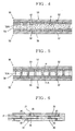
- a sheet-forming material composed of a conductive paste composition in which the specific conductive particles P exhibiting magnetism are dispersed in a polymeric substance-forming material is first prepared, and the sheet-forming material is filled into the cavity of the mold as illustrated in Fig. 4, thereby forming a sheet-forming material layer 10A.
- a pair of electromagnets are then arranged on the upper surface of the base plate 51 in the top force 50 and the lower surface of the base plate 56 in the bottom force 55, and the electromagnets are operated, thereby applying a parallel magnetic field having an intensity distribution, i.e., a parallel magnetic field having higher intensity at portions between ferromagnetic material portions 52 in the top force 50 and their corresponding ferromagnetic material portions 57 in the bottom force 55, to the sheet-forming material layer 10A in the thickness-wise direction thereof.
- the specific conductive particles P dispersed in the sheet-forming material layer 10A are gathered at portions 11A to become the conductive parts, which are located between the ferromagnetic material portions 52 in the top force 50 and their corresponding ferromagnetic material portions 57 in the bottom force 55, as illustrated in Fig. 5, and at the same time oriented so as to be arranged in the thickness-wise direction of the sheet-forming material layer 10A.
- the sheet-forming material layer 10A is subjected to a curing treatment, thereby producing an anisotropically conductive sheet 10 comprising conductive parts 11 arranged between the ferromagnetic material portions 52 in the top force 50 and their corresponding ferromagnetic material portions 57 in the bottom force 55, in which the specific conductive particles P are closely filled in the elastic polymeric substance, and insulating part 12 composed of the elastic polymeric substance, in which the specific conductive particles P are not present at all or scarcely present.
- the curing treatment of the sheet-forming material layer 10A may be conducted in the state that the parallel magnetic field is being applied. However, the treatment may also be conducted after stopping the application of the parallel magnetic field.
- the intensity of the parallel magnetic field applied to the sheet-forming material layer 10A is preferably an intensity that it amounts to 0.1 to 2 T on the average.
- permanent magnets may also be used in place of the electromagnets.
- permanent magnets are preferred those composed of alunico (Fe-Al-Ni-Co alloy), ferrite or the like in that the intensity of the parallel magnetic field within the above range is achieved.
- the curing treatment of the sheet-forming material layer 10A is suitably selected according to the material used. However, the treatment is generally conducted by a heat treatment. Specific heating temperature and heating time are suitably selected in view of the kind of the addition type liquid silicone rubber or the like making up the sheet-forming material layer 10A, the time required for movement of the conductive particles, and the like.
- Such an anisotropically conductive sheet 10 is suitable for use as a connector for achieving electrical connection between, for example, a printed circuit board and a leadless chip carrier, liquid crystal panel or the like in fields of electronic computers, electronic digital clocks, electronic cameras and computer key boards, or in electrical inspection of circuit devices such as printed circuit boards, semiconductor integrated circuit devices and wafers on the surface of which a number of integrated circuits have been formed, as a connector for achieving electrical connection between electrodes to be inspected formed on a surface of a circuit device, which is an inspection target, and electrodes for inspection formed on the surface of a circuit board for inspection.
- the circuit board according to the present invention comprises a conductor containing the above-described conductive metal particles and/or the above-described conductive composite metal particles.
- Fig. 6 is a cross-sectional view illustrating the construction of principal parts in an exemplary circuit board according to the present invention.
- This circuit board is a multi-layer printed circuit board and is constructed by laminating a first insulating layer 20, a second insulating layer 30 and a third insulating layer 40 in this order from above.
- a first inner wiring layer 26 is formed between the first insulating layer 20 and the second insulating layer 30, and a second inner wiring layer 36 is formed between the second insulating layer 30 and the third insulating layer 40.
- First interlayer short circuit parts 25, second interlayer short circuit parts 35 and third interlayer short circuit parts 45 are provided in the first insulating layer 20, the second insulating layer 30 and the third insulating layer 40, respectively, so as to extend in their thickness-wise directions.
- the upper-side wiring layer 21 is electrically connected to the first inner wiring layer 26 through the first interlayer short circuit parts 25, the first inner wiring layer 26 is electrically connected to the second inner wiring layer 36 through the second interlayer short circuit parts 35, and the second inner wiring layer 36 is electrically connected to the lower-side wiring layer 41 through the third interlayer short circuit parts 45.
- each of the first insulating layer 20, the second insulating layer 30 and the third insulating layer 40 is preferably used an insulating resin material high in heat resistance.
- an insulating resin material high in heat resistance include glass fiber-reinforced epoxy resins, glass fiber-reinforced polyimide resins, glass fiber-reinforced phenol resins, glass fiber-reinforced bismaleimidotriazine resins and glass fiber-reinforced aramide resins.
- the first interlayer short circuit parts 25, the second interlayer short circuit parts 35 and the third interlayer short circuit parts 45 are each formed by a conductor containing the specific conductive particles P in an organic polymeric substance.
- the specific conductive particles P are bound to the organic polymeric substance in a state oriented so as to be arranged in the thickness-wise direction of the insulating layer concerned.
- thermosetting resin such as an epoxy resin, polyimide resin, phenol resin, bismaleimidotriazine resin, or a cured product of liquid rubber such as silicone rubber or urethane rubber.
- the specific conductive particles P are preferably contained in a proportion of 30 to 60%, more preferably 35 to 50 in terms of volume fraction. If this proportion is lower than 30%, any interlayer short circuit part sufficiently low in electric resistance may not be obtained in some cases. If this proportion exceeds 60% on the other hand, the resulting short circuit parts become fragile, so that necessary strength and durability may not be achieved in some cases.
- the above-described circuit board can be produced in the following manner.
- a second insulating layer-forming material (material for forming the second insulating layer 30) 30A in the form of a sheet composed of a thermosetting resin material in a semi-cured state is provided.
- through-holes 35H passing through in the thickness-wise direction of the second insulating layer-forming material 30A are bored at portions of the second insulating layer-forming material 30A, where the second interlayer short circuit parts are to be formed.
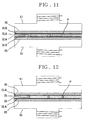
- a short circuit-forming material composed of a conductive paste composition with the specific conductive particles P exhibiting magnetism contained in a liquid thermosetting resin material is then filled into each of the through-holes 35H bored in the second insulating layer-forming material 30A, the short circuit-forming material is subjected to a heat treatment, thereby forming a short circuit part-forming material layer 35A in each of the through-holes 35H in the second insulating layer-forming material 30A as illustrated in Fig. 9.
- This short circuit part-forming material layer 35A is in a state that the form of the short circuit part-forming material layer 35A is retained, and it has been semi-cured to an extent that the specific conductive particles P can be moved in the short circuit part-forming material layer 35A.
- a means for making the through-holes 35H in the second insulating layer-forming material 30A in the above process may be used a means by laser processing, a means by drilling, a means by punching, or the like.
- a printing method such as screen printing, roll pressing, or the like.
- the heat treatment of the short circuit-forming material is conducted under conditions that the cure of the second insulating layer-forming material 30A is not caused to progress.
- Specific conditions of the heat treatment are suitably preset according to the kinds of the second insulating layer-forming material 30A and the short circuit-forming material.
- the heating temperature is 80 to 100°C
- the heating time is 20 to 60 minutes.
- the second insulating layer-forming material 30A and the short circuit-forming material layer 35A are subjected to a heat treatment while applying a parallel magnetic field to the short circuit-forming material layer 35A in the thickness-wise direction thereof in a state that the metal foil 26B, the second insulating layer-forming material 30A and the metal foil 36B have been pressurized in the thickness-wise direction thereof, thereby compressing the second insulating layer-forming material 30A and the short circuit-forming material layer 35A in the thickness-wise direction.
- magnetic pole plates 60 and 65 composed of a ferromagnetic material are arranged on the upper surface of the metal foil 26B and the lower surface of the metal foil 36B, respectively, and a pair of electromagnets 61 and 66 are further arranged on the upper surface of the magnetic pole plate 60 and the lower surface of the magnetic pole plate 65, respectively.
- the electromagnets 61, 66 are operated in a state that the metal foil 26B, the second insulating layer-forming material 30A and the metal foil 36B are pressurized in the thickness-wise direction thereof, thereby applying a parallel magnetic field to the short circuit-forming material layer 35A in the thickness-wise direction thereof and at the same time subjecting the second insulating layer-forming material 30A and the short circuit-forming material layer 35A to a heat treatment.
- the ferromagnetic material making up the magnetic pole plates 60, 65 may be used iron, nickel, cobalt or an alloy thereof.
- the pressurizing conditions for the metal foil 26B, the second insulating layer-forming material 30A and the metal foil 36B are generally 5 to 50 kg/cm 2 .
- the intensity of the parallel magnetic field applied to the short circuit-forming material layer 35A is preferably 0.1 to 2 T on the average.
- permanent magnets may also be used in place of the electromagnets.
- permanent magnets are preferred those composed of alunico (Fe-Al-Ni-Co alloy), ferrite or the like in that the intensity of the parallel magnetic field within the above range is achieved.
- the conditions for the heat treatment are suitably selected according to the kinds of the second insulating layer-forming material 30A and the short circuit-forming material.
- the heating temperature is 150 to 180°C
- the heating time is 1 to 4 hours.
- the parallel magnetic field is applied to the short circuit-forming material layer 35A in the thickness-wise direction thereof, whereby the specific conductive particles P dispersed in the short circuit-forming material layer 35A are oriented so as to be arranged in the thickness-wise direction of the short circuit-forming material layer 35A, and the second insulating layer-forming material 30A and the short circuit-forming material layer 35A are cured by the heat treatment, whereby the second insulating layer 30 and the second interlayer short circuit parts 35 are formed as illustrated in Fig.
- the metal foils 26B and 36B are integrally fixed on the upper surface and lower surface of the second insulating layer 30, respectively, thereby thus obtaining a laminate in which a thin metal layer 26A, the second insulating layer 30 and a thin metal layer 36A have been laminated on one another in this order from above.
- resist layers 33 and 34 are formed on the thin metal layers 26A and 36A provided on the upper and lower surfaces of the second insulating layer 30, respectively, so as to cover portions which will become a first inner wiring layer and a second inner wiring layer, and exposed portions of the thin metal layers 26A and 36A are removed by an etching treatment, thereby forming a first inner wiring layer 26 and a second inner wiring layer 36 between the second insulating layer 30 and the resist layers 33, 34, respectively.
- an intermediate base 7 having the first inner wiring layer 26 and the second inner wiring layer 36 on both surfaces of the second insulating layer 30 is obtained.
- the resist layers 33, 34 are removed from the surfaces of the first inner wiring layer 26 and the second inner wiring layer 36.
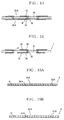
- an intermediate material 8 for a first insulating layer (illustrated in Fig. 15A) with a short circuit part-forming material layer 25A formed in each of through-holes 25H bored in a first insulating layer-forming material (material for forming a first insulating layer) 20A in the form of a sheet composed of a thermosetting resin material in a semi-cured state, and an intermediate material 9 for a third insulating layer (illustrated in Fig.
- a process for forming the short circuit part-forming material layers 25A, 45A in the first insulating layer-forming material 20A and the third insulating layer-forming material 40A may be performed in accordance with the process for forming the short circuit part-forming material layer 35A in the second insulating layer-forming material 30A.
- the intermediate material 8 for the first insulating layer is arranged on the upper surface of the intermediate base 7, and a metal foil 21B is further arranged on the upper surface of the intermediate material 8 for the first insulating layer, and moreover the intermediate material 9 for the third insulating layer is arranged on the lower surface of the intermediate base 7, and a metal foil 41B is further arranged on the lower surface of the intermediate material 9 for the third insulating layer.
- the first insulating layer-forming material 20A, the third insulating layer-forming material 40A, the short circuit-forming material layer 25A and the short circuit-forming material layer 45A are subjected to a heat treatment while applying a parallel magnetic field to the short circuit-forming material layer 25A and the short circuit-forming material layer 45A in the thickness-wise direction thereof in a state that the metal foil 21B, the intermediate material 8 for the first insulating layer, the intermediate base 7, the intermediate material 9 for the third insulating layer and the metal foil 41B are pressurized in the thickness-wise direction thereof, thereby forming a first insulating layer 20, a third insulating layer 40, a first interlayer short circuit part 25 and a third interlayer short circuit part 45 as illustrated in Fig. 17.
- first insulating layer 20 and the third insulating layer 40 are integrally fixed on the upper surface and lower surface of the second insulating layer 30, respectively, and moreover the metal foil 21B is integrally fixed on the upper surface of the first insulating layer 20 and the metal foil 41B is integrally fixed on the lower surface of the third insulating layer 40, thereby thus obtaining a laminate in which a thin metal layer 21A, the first insulating layer 20, the second insulating layer 30, the third insulating layer 40 and a thin metal layer 41A are laminated on one another in this order from above.
- resist layers 22 and 42 are formed on the thin metal layers 21A and 41A provided on the upper surface of the first insulating layer 20 and the lower surface of the third insulating layer 40, respectively, so as to cover portions which will become an upper-side wiring layer and a lower-side wiring layer, and exposed portions of the thin metal layers 21A and 41A are removed by an etching treatment, thereby forming an upper-side wiring layer 21 between the first insulating layer 20 and the resist layer 22, and a lower-side wiring layer 41 between the third insulating layer 40 and the resist layer 42, as illustrated in Fig.19. Thereafter, the resist layers 22, 42 are removed, thereby obtaining a circuit board of the construction shown in Fig. 6.
- the specific conductive particles P are contained in a state oriented so as to be arranged in the thickness-wise direction of each insulating layer, a conductive path is formed by a chain of the specific conductive particles P in each interlayer short circuit part. As a result, still higher conductivity is achieved.
- each of the first interlayer short circuit parts 25, the second interlayer short circuit parts 35 and the third interlayer short circuit parts 45 photolithography is useless because the short circuit-forming material composed of the conductive paste composition is used. Therefore, the first interlayer short circuit parts 25, the second interlayer short circuit parts 35 and the third interlayer short circuit parts 45 can be formed by a simple process, and moreover still higher connection reliability is achieved because no chemical is used.
- conductive particles exhibiting magnetism are used as the specific conductive particles P making up each short circuit part, whereby the specific conductive particles P can be easily oriented so as to be arranged in the thickness-wise direction of each insulating layer by applying a magnetic field to the short circuit-forming material layers 25A, 35A and 45A.
- the respective insulating layer-forming materials and short circuit part-forming material layers are subjected to a heat treatment while applying a magnetic field to the respective short circuit part-forming material layers under pressure, whereby the specific conductive particles P can be surely oriented so as to be arranged in the thickness-wise direction of each insulating layer concerned.
- thermosetting resin or rubber low in elastic modulus is used as an organic polymeric substance forming the interlayer short circuit parts, thereby bring about the following effect. Namely, when a multi-layer printed circuit board is constructed, in which insulating layers different in material from each other are laminated, stress to be caused at interlayer short circuit parts due to a difference in coefficient of thermal expansion between the materials for forming the respective insulating layers can be relaxed by the elastic force of the interlayer short circuit parts.
- Such a circuit board is suitable for use as a circuit board for electronic part for forming an electronic part such as a chip carrier or MCM, a circuit board for mounting electronic parts, such as a mother board for example, or an adapter used in electrical inspection for circuit devices.
- Fig. 20 is a cross-sectional view illustrating the construction of an exemplary conductive connection structure according to the present invention.
- an electronic part 71 is fixed on a circuit board 73 by a connecting member 70 formed by the conductive paste composition described above, and electrodes 72 of the electronic part 71 are electrically connected to electrodes 74 of the circuit board 73 through the connecting member 70.
- the electronic part 71 No particular limitation is imposed on the electronic part 71, and various electronic parts may be used. Examples thereof include active parts composed of each of semiconductor devices such as transistors, diodes, relays, switches, IC chips or LSI chips or packages thereof, and MCM (multi chip module); passive parts such as resistors, capacitors, quartz oscillators, speakers, microphones, transformers (coils) and inductors; and display panels such as TFT type liquid crystal display panels, STN type liquid crystal display panels, plasma display panels and electroluminescence panels.
- semiconductor devices such as transistors, diodes, relays, switches, IC chips or LSI chips or packages thereof, and MCM (multi chip module)
- passive parts such as resistors, capacitors, quartz oscillators, speakers, microphones, transformers (coils) and inductors
- display panels such as TFT type liquid crystal display panels, STN type liquid crystal display panels, plasma display panels and electroluminescence panels.
- the circuit board 73 may be used any of various structures such as single-side printed circuit boards, double-side printed circuit boards and multi-layer printed circuit boards.
- the circuit board 73 may be any of a flexible board, a rigid board and a flexible-rigid board composed of a combination thereof.
- a material for forming the flexible board may be used polyimide, polyamide, polyester, polysulfone or the like.
- a material for forming the rigid board may be used a composite resin material such as a glass fiber-reinforced epoxy resin, glass fiber-reinforced phenol resin, glass fiber-reinforced polyimide resin or glass fiber-reinforced bismaleimidotriazine resin, or a ceramic material such as silicon dioxide or alumina.
- a composite resin material such as a glass fiber-reinforced epoxy resin, glass fiber-reinforced phenol resin, glass fiber-reinforced polyimide resin or glass fiber-reinforced bismaleimidotriazine resin, or a ceramic material such as silicon dioxide or alumina.
- Examples of materials for the electrodes 72 in the electronic part 71 and the electrodes 74 in the circuit board 73 include gold, silver, copper, nickel, palladium, carbon, aluminum and ITO.
- the thicknesses of the electrodes 72 in the electronic part 71 and the electrodes 74 in the circuit board 73 are each preferably 0.1 to 100 ⁇ m.
- the widths of the electrodes 72 in the electronic part 71 and the electrodes 74 in the circuit board 73 are each preferably 1 to 500 ⁇ m.
- Such a conductive connection structure can be fabricated by coating surface or surfaces of one or both of the electronic part 71 and the circuit board 73 with the conductive paste composition described above, arranging the electronic part 71 on the surface of the circuit board 73 in an aligned state and then subjecting the conductive paste composition to a curing treatment or drying treatment, or by forming the conductive paste composition into a film, making the film a semi-cured state and then arranging this film between the electronic part 71 and the circuit board 73 to conduct a curing treatment.
- the specific conductive particles can be oriented so as to be arranged in the thickness-wise direction by applying a magnetic field to the conductive paste composition in the thickness-wise direction thereof before conducting a curing treatment or drying treatment of the conductive paste composition or while conducting such a treatment, whereby electrical connection can be achieved with higher conductivity.
- Fig. 21 is a cross-sectional view illustrating the construction of another exemplary conductive connection structure according to the present invention.
- an electronic part 71 is arranged on a circuit board 73 with an interposed anisotropically conductive sheet 10, for example, of the construction shown in Fig. 2.
- the anisotropically conductive sheet 10 is fixed by a fixing member 75 in a state held pressurized by and between the electronic part 71 and the circuit board 73.
- Electrodes 72 in the electronic part 71 are electrically connected to electrodes 74 in the circuit board 73 through conductive parts 11 in the anisotropically conductive sheet 10.
- the electronic part 71 is connected to the circuit board 73 through the connecting member 70 formed by the conductive paste composition, or through the anisotropically conductive sheet 10, as described above. Therefore, electrical connection high in conductivity and reproductivity thereof can be achieved between the electronic part 71 and the circuit board 73.
- Fig. 22 is a cross-sectional view illustrating the construction of principal parts of an exemplary electrical inspection apparatus for circuit devices according to the present invention.
- reference numeral 80 indicates an adapter composed of a printed circuit board. Electrodes 81 for inspection are arranged on the surface (upper surface in Fig. 22) of the adapter 80 according to a pattern corresponding to electrodes 77 to be inspected in a circuit device 76 to be inspected.
- This adapter 80 is provided with a plurality of positioning pins 83 extending perpendicularly to the surface of the adapter 80.
- Reference numeral 15 indicates a connector in the form of a sheet, which is constructed by an anisotropically conductive sheet 10 of the structure shown in Fig. 2 and a frame-like support 16 for supporting the peripheral part of the anisotropically conductive sheet 10.
- Positioning holes 17 are formed correspondingly to the positioning pins 83 in the support 16.
- This connector 15 is arranged on the surface of the adapter 80 in a state positioned by inserting the positioning pins through the positioning holes 17 in the support 16 thereof.
- Reference numeral 85 designates a holding plate for holding the circuit device 76 to be inspected.
- An opening 86, in which the circuit device 76 to be inspected is arranged, is defined at the center thereof, and positioning holes 87 are formed correspondingly to the positioning pins 83 at peripheral portions thereof.
- This holding plate 85 is arranged above the sheet-like connector 15 in a state positioned by slidably movably inserting the positioning pins 83 through the positioning holes 87.
- Examples of the circuit device 76 to be inspected which is an inspection target, include wafers, semiconductor chips, packages such as BGA and CSP, modules such as MCM, and circuit boards such as single-side printed circuit boards, double-side printed circuit boards and multi-layer printed circuit boards.
- the circuit device 76 to be inspected is fixed in the opening 86 in the holding member 85, and the circuit device 76 to be inspected is moved in a direction (downward direction in Fig. 22) coming close to the connector 15, so that a state is accomplished wherein the anisotropically conductive sheet 10 in the connector 15 is pressurized by and between the circuit device 76 to be inspected and the adapter 80.
- electrical connection between the electrodes 77 to be inspected in the circuit device 76 to be inspected and the electrodes 81 for inspection in the adapter 80 is achieved through the conductive parts 11 in the anisotropically conductive sheet 10.
- FC1000 Conductive Metal Particles
- An air classifier "Turboclassifier TC-15N" (manufactured by Nissei Engineering Co., Ltd.) was used to classify 2 kg of nickel particles under conditions of a specific gravity of 8.9, an air flow rate of 2.5 m 3 /min, a rotor speed of 2250 rpm, a classification point of 15 ⁇ m and a feed rate of nickel particles of 50 g/min, thereby collecting 1.1 kg of nickel particles, and 1.1 kg of the nickel particles were further classified under conditions of a specific gravity of 8.9, an air flow rate of 2.5 m 3 /min, a rotor speed of 3750 rpm, a classification point of 7 ⁇ m and a feed rate of nickel particles of 50 g/min to collect 0.8 kg of nickel particles.
- a sonic sifter "SW-20AT Model" manufactured by Tsutsui Rikagaku Kiki K.K. was then used to further classify 500 g of the nickel particles classified by the air classifier. Specifically, 4 sieves each having a diameter of 200 mm and respectively having opening diameters of 32 ⁇ m, 20 ⁇ m, 12.5 ⁇ m and 8 ⁇ m were superimposed on one another in this order from above.
- Each of the sieves was charged with 10 g of ceramic balls having a diameter of 2 mm, and 20 g of the nickel particles were placed on the uppermost sieve (opening diameter: 32 ⁇ m) to classify them under conditions of 112 Hz for 15 minutes and 224 Hz for 15 minutes, thereby collecting nickel particles captured on the lowest sieve (opening diameter: 8 ⁇ m). This process was conducted repeatedly 25 times in total, thereby preparing 10 g of Conductive Metal Particles [A] according to the present invention.
- the Conductive Metal Particles [A] thus obtained had a number average particle diameter of 10 ⁇ m, a coefficient of variation of the particle diameter of 10%, a BET specific surface area of 0.5 x 10 3 m 2 /kg, a sulfur element content of 0.05% by mass, an oxygen element content of 0.02% by mass, a carbon element content of 0.03% by mass and a saturation magnetization of 0.6 Wb/m 2 .
- Conductive Metal Particles [B] to [G] were prepared in the same manner as in the preparation of Conductive Metal Particles [A] except that the conditions of the air classifier and the sonic sifter were changed.
- Conductive metal particles composed of nickel having a number average particle diameter of 65 ⁇ m, a coefficient of variation of the particle diameter of 40%, a BET specific surface area of 0.03 x 10 3 m 2 /kg, a sulfur element content of 0.08% by mass, an oxygen element content of 0.02% by mass, a carbon element content of 0.05% by mass and a saturation magnetization of 0.6 Wb/m 2 .
- Conductive metal particles composed of nickel having a number average particle diameter of 120 ⁇ m, a coefficient of variation of the particle diameter of 48%, a BET specific surface area of 0.02 x 10 3 m 2 /kg, a sulfur element content of 0.07% by mass, an oxygen element content of 0.2% by mass, a carbon element content of 0.04% by mass and a saturation magnetization of 0.6 Wb/m 2 .
- Conductive metal particles composed of nickel having a number average particle diameter of 4 ⁇ m, a coefficient of variation of the particle diameter of 7%, a BET specific surface area of 0.7 x 10 3 m 2 /kg, a sulfur element content of 0.03% by mass, an oxygen element content of 0.1% by mass, a carbon element content of 0.03% by mass and a saturation magnetization of 0.6 Wb/m 2 .
- Conductive metal particles composed of nickel having a number average particle diameter of 5 ⁇ m, a coefficient of variation of the particle diameter of 47%, a BET specific surface area of 0.9 x 10 3 m 2 /kg, a sulfur element content of 0.07% by mass, an oxygen element content of 0.2% by mass, a carbon element content of 0.04% by mass and a saturation magnetization of 0.6 Wb/m 2 .
- Conductive metal particles composed of nickel having a number average particle diameter of 73 ⁇ m, a coefficient of variation of the particle diameter of 58%, a BET specific surface area of 0.05 x 10 3 m 2 /kg, a sulfur element content of 0.1% by mass, an oxygen element content of 0.6% by mass, a carbon element content of 0.12% by mass and a saturation magnetization of 0.6 Wb/m 2 .
- Conductive metal particles composed of nickel having a number average particle diameter of 48 ⁇ m, a coefficient of variation of the particle diameter of 32%, a BET specific surface area of 0.08 x 10 3 m 2 /kg, a sulfur element content of 0.14% by mass, an oxygen element content of 0.8% by mass, a carbon element content of 0.13% by mass and a saturation magnetization of 0.6 Wb/m 2 .
- Conductive Metal Particles [A] subjected to the acid treatment and washing treatment were added 2 L of a plating solution containing gold in a proportion of 20 g/L.
- the temperature of the treating vessel was raised to 90°C and stirred, thereby preparing a slurry. While stirring the slurry in this state, Conductive Metal Particles [A] was subjected to plating with gold. Thereafter, the slurry was left at rest while allowing it to cool, thereby precipitating particles, and a supernatant was removed to prepare Conductive Composite Metal Particles [a1] according to the present invention.
- the Conductive Composite Metal Particles [a1] thus obtained had a number average particle diameter of 15 ⁇ m, a BET specific surface area of 0.2 x 10 3 m 2 /kg, a thickness t of the coating layer of 89 nm, a gold content at the surface layer portion of 82% by mass and an electric resistance value R of 0.03 ⁇ .
- Conductive Composite Metal Particles [a2] for reference were prepared in the same manner as in the preparation of Conductive Composite Metal Particles [a1] except that the content of gold in the plating solution was changed to 5 g/L.
- the Conductive Composite Metal Particles [a2] thus obtained had a number average particle diameter of 12 ⁇ m, a BET specific surface area of 0.4 x 10 3 m 2 /kg, a thickness t of the coating layer of 8 nm, a gold content at the surface layer portion of 38% by mass and an electric resistance value R of 5 ⁇ .
- Conductive Composite Metal Particles [b1] and [b2] were prepared in the same manner as in the preparation of Conductive Composite Metal Particles [a1] except that Conductive Metal Particles [B] were used in place of Conductive Metal Particles [A], and the content of gold in the plating solution was changed.
- Conductive composite metal particles having a number average particle diameter of 72 ⁇ m, a BET specific surface area of 0.02 x 10 3 m 2 /kg, a thickness t of the coating layer of 65 nm, a gold content at the surface layer portion of 66% by mass and an electric resistance value R of 0.1 ⁇ .
- Conductive composite metal particles having a number average particle diameter of 130 ⁇ m, a BET specific surface area of 0.009 x 10 3 m 2 /kg, a thickness t of the coating layer of 57 nm, a gold content at the surface layer portion of 63% by mass and an electric resistance value R of 1.1 ⁇ .
- Conductive Composite Metal Particles [c1] were prepared in the same manner as in the preparation of Conductive Composite Metal Particles [a1] except that Conductive Metal Particles [C] were used in place of Conductive Metal Particles [A], and the content of gold in the plating solution was changed.
- Conductive composite metal particles having a number average particle diameter of 127 ⁇ m, a BET specific surface area of 0.01 x 10 3 m 2 /kg, a thickness t of the coating layer of 52 nm, a gold content at the surface layer portion of 57% by mass and an electric resistance value R of 0.3 ⁇ .
- Conductive Composite Metal Particles [d1] were prepared in the same manner as in the preparation of Conductive Composite Metal Particles [a1] except that Conductive Metal Particles [D] were used in place of Conductive Metal Particles [A], and the content of gold in the plating solution was changed.
- Conductive composite metal particles having a number average particle diameter of 6 ⁇ m, a BET specific surface area of 0.6 x 10 3 m 2 /kg, a thickness t of the coating layer of 37 nm, a gold content at the surface layer portion of 33% by mass and an electric resistance value R of 2 ⁇ .
- Conductive Composite Metal Particles [e1] were prepared in the same manner as in the preparation of Conductive Composite Metal Particles [a1] except that Conductive Metal Particles [E] were used in place of Conductive Metal Particles [A], and the content of gold in the plating solution was changed.
- Conductive composite metal particles having a number average particle diameter of 6 ⁇ m, a BET specific surface area of 0.8 x 10 3 m 2 /kg, a thickness t of the coating layer of 77 nm, a gold content at the surface layer portion of 69% by mass and an electric resistance value R of 0.5 ⁇ .
- Conductive Composite Metal Particles [f1] were prepared in the same manner as in the preparation of Conductive Composite Metal Particles [a1] except that Conductive Metal Particles [F] were used in place of Conductive Metal Particles [A], and the content of gold in the plating solution was changed.
- Conductive composite metal particles having a number average particle diameter of 79 ⁇ m, a BET specific surface area of 0.06 x 10 3 m 2 /kg, a thickness t of the coating layer of 74 nm, a gold content at the surface layer portion of 67% by mass and an electric resistance value R of 0.8 ⁇ .
- Conductive Composite Metal Particles [g1] were prepared in the same manner as in the preparation of Conductive Composite Metal Particles [a1] except that Conductive Metal Particles [G] were used in place of Conductive Metal Particles [A], and the content of gold in the plating solution was changed.
- Conductive composite metal particles having a number average particle diameter of 53 ⁇ m, a BET specific surface area of 0.05 x 10 3 m 2 /kg, a thickness t of the coating layer of 75 nm, a gold content at the surface layer portion of 82% by mass and an electric resistance value R of 0.4 ⁇ .
- Liquid A and Liquid B of addition type liquid silicone rubber "KE1950-40" product of Shin-Etsu Chemical Co., Ltd. were mixed with each other in equal proportions (in terms of weight), and 100 parts by weight of Conductive Composite Metal Particles [a1] were then added to 100 parts by weight of this mixture.
- the resultant mixture was subjected to a defoaming treatment by pressure reduction, thereby preparing Conductive Paste Composition (1) according to the present invention.
- liquid silicone rubber "KE1950-40” With respect to the addition type liquid silicone rubber "KE1950-40", the viscosities (as determined by a Brookfield type viscometer) of Liquid A and Liquid B at 23°C are both 4,800 P, the compression permanent set (JIS K 6249) at 150°C of the cured product thereof is 20%, the durometer hardness A (JIS K 6249) at 23°C is 42, and the tensile strength (JIS K 6249, crescent type) is 35.6 kgf/cm.
- Conductive Paste Composition (2) according to the present invention was prepared in the same manner as in Preparation Example 1 except that Conductive Composite Metal Particles [b1] were used in place of Conductive Composite Metal Particles [a1].
- a comparative Conductive Paste Composition (3) was prepared in the same manner as in Preparation Example 1 except that Conductive Composite Metal Particles [c1] were used in place of Conductive Composite Metal Particles [a1].
- a comparative Conductive Paste Composition (4) was prepared in the same manner as in Preparation Example 1 except that Conductive Composite Metal Particles [d1] were used in place of Conductive Composite Metal Particles [a1].
- a comparative Conductive Paste Composition (5) was prepared in the same manner as in Preparation Example 1 except that Conductive Composite Metal Particles [e1] were used in place of Conductive Composite Metal Particles [a1].
- a comparative Conductive Paste Composition (6) was prepared in the same manner as in Preparation Example 1 except that Conductive Composite Metal Particles [f1] were used in place of Conductive Composite Metal Particles [a1].
- a comparative Conductive Paste Composition (7) was prepared in the same manner as in Preparation Example 1 except that Conductive Composite Metal Particles [g1] were used in place of Conductive Composite Metal Particles [a1].
- a referential Conductive Paste Composition (8) was prepared in the same manner as in Preparation Example 1 except that Conductive Composite Metal Particles [a2] were used in place of Conductive Composite Metal Particles [a1].
- a referential Conductive Paste Composition (9) was prepared in the same manner as in Preparation Example 1 except that Conductive Composite Metal Particles [b2] were used in place of Conductive Composite Metal Particles [a1].
- a circuit board having a lead electrode region in which 240 linear lead electrodes each having a width of 0.15 mm and composed of copper were arranged in parallel with one another at a pitch of 0.25 mm (clearance: 0.1 mm), was provided, and a conductive paste composition sample was coated on the lead electrode region of the circuit board by screen printing, thereby forming a coating layer having a width of 1.0 mm and a thickness of about 0.3 mm and extending in a direction perpendicular to the direction in which the lead electrodes extend.
- the coating layer was subjected to a curing treatment under conditions of 150°C and 1 hour, thereby forming an anisotropically conductive connection member integrally provided on the lead electrode region of the circuit board.
- the flat board was pressed down repeatedly at a cycle of 1 Hz under an environment of 25°C in temperature and 30% in relative humidity, thereby measuring electric resistances between the lead electrodes of the circuit board and the common electrode of the flat board after pressing 10,000 times to find the average value thereof.
- a mold for production of anisotropically conductive sheets was fabricated under the following conditions in accordance with the construction basically shown in Fig. 3 except that a space region for arrangement of a support was provided in a cavity.
- a frame-like support for anisotropically conductive sheet composed of stainless steel and having a thickness of 0.2 mm was arranged in the space region for arrangement of the support within the cavity of the mold.
- Conductive Paste Composition (1) was then filled into the cavity of the mold and subjected to a defoaming treatment by pressure reduction, thereby forming a conductive composition layer in the mold.
- the conductive composition layer was subjected to a curing treatment under conditions of 100°C for 1 hour. After removing it from the mold, post curing was conducted under conditions of 200°C for 4 hours, thereby producing a support-equipped anisotropically conductive sheet (1) according to the present invention, which has a plurality of conductive parts each extending in the thickness-wise direction of the sheet, and insulating part insulating these conductive parts mutually.
- the anisotropically conductive sheet (1) thus obtained was such that the conductive parts each having an external diameter of 0.25 mm were arranged in 16 lines and 16 rows at a pitch of 0.5 mm.
- the thickness of the insulating part was 0.3 mm
- the thickness of each of the conductive parts was 0.4 mm
- the conductive parts were formed in a state projected (each projected height: 0.05 mm) from both surfaces of the insulating part.
- a support-equipped anisotropically conductive sheet (2) according to the present invention was produced in the same manner as in Production Example 1 except that Conductive Paste Composition (2) was used in place of Conductive Paste Composition (1).
- a comparative support-equipped anisotropically conductive sheet (3) was produced in the same manner as in Production Example 1 except that Conductive Paste Composition (3) was used in place of Conductive Paste Composition (1).
- a comparative support-equipped anisotropically conductive sheet (4) was produced in the same manner as in Production Example 1 except that Conductive Paste Composition (4) was used in place of Conductive Paste Composition (1).
- a comparative support-equipped anisotropically conductive sheet (5) was produced in the same manner as in Production Example 1 except that Conductive Paste Composition (5) was used in place of Conductive Paste Composition (1).
- a comparative support-equipped anisotropically conductive sheet (6) was produced in the same manner as in Production Example 1 except that Conductive Paste Composition (6) was used in place of Conductive Paste Composition (1).
- a comparative support-equipped anisotropically conductive sheet (7) was produced in the same manner as in Production Example 1 except that Conductive Paste Composition (7) was used in place of Conductive Paste Composition (1).
- a referential support-equipped anisotropically conductive sheet (8) was produced in the same manner as in Production Example 1 except that Conductive Paste Composition (8) was used in place of Conductive Paste Composition (1).
- a referential support-equipped anisotropically conductive sheet (9) was produced in the same manner as in Production Example 1 except that Conductive Paste Composition (9) was used in place of Conductive Paste Composition (1).
- the anisotropically conductive sheets (1) to (9) according to Production Examples 1 and 2, Comparative Production Examples 1 to 5 and Referential Production Examples 1 and 2 were evaluated in the following manner.
- conductive materials having stable conductivity can be provided.
- the conductive paste compositions according to the present invention have high conductivity and are high in reproductivity thereof because the above-described conductive metal particles and/or conductive composite metal particles are contained.
- the conductive sheets according to the present invention have high conductivity and are high in reproductivity thereof because the above-described conductive metal particles and/or conductive composite metal particles are contained.
- the circuit boards according to the present invention have high conductivity between wiring layers and are high in reproductivity thereof because they have a conductor containing the above-described conductive metal particles and/or conductive composite metal particles.
- conductive connection structures of the present invention electrical connection high in conductivity and the reproductivity thereof can be achieved because they are connected by the above-described conductive paste composition or through the above-described conductive sheet.
- electrical connection high in conductivity and the reproductivity thereof can be achieved to a circuit device which is an inspection target because the apparatus have the above-described conductive sheet.
- the conductive metal particles have a number average particle diameter of 5 to 100 ⁇ m, a BET specific surface area of 0.01 x 10 3 to 0.7 x 10 3 m 2 /kg, a sulfur element content of at most 0.1% by mass, an oxygen element content of at most 0.5% by mass and a carbon element content of at most 0.1% by mass.
- the conductive composite metal particles are obtained by coating the surfaces of the conductive metal particles with a high-conductive metal.
Landscapes
- Chemical & Material Sciences (AREA)
- Dispersion Chemistry (AREA)
- Engineering & Computer Science (AREA)
- Microelectronics & Electronic Packaging (AREA)
- Physics & Mathematics (AREA)
- Spectroscopy & Molecular Physics (AREA)
- Conductive Materials (AREA)
- Non-Insulated Conductors (AREA)
- Powder Metallurgy (AREA)
- Compositions Of Macromolecular Compounds (AREA)
Applications Claiming Priority (2)
| Application Number | Priority Date | Filing Date | Title |
|---|---|---|---|
| JP2000300028 | 2000-09-29 | ||
| JP2000300028 | 2000-09-29 |
Publications (3)
| Publication Number | Publication Date |
|---|---|
| EP1193757A2 true EP1193757A2 (de) | 2002-04-03 |
| EP1193757A3 EP1193757A3 (de) | 2005-09-28 |
| EP1193757B1 EP1193757B1 (de) | 2008-12-10 |
Family
ID=18781760
Family Applications (1)
| Application Number | Title | Priority Date | Filing Date |
|---|---|---|---|
| EP01123036A Expired - Lifetime EP1193757B1 (de) | 2000-09-29 | 2001-09-26 | Leitende Metall-, Verbindungsmetall-Teilchen und deren Produktanwendungen |
Country Status (8)
| Country | Link |
|---|---|
| US (2) | US6663799B2 (de) |
| EP (1) | EP1193757B1 (de) |
| KR (3) | KR20020025796A (de) |
| CN (1) | CN1229817C (de) |
| AT (1) | ATE417359T1 (de) |
| DE (1) | DE60136897D1 (de) |
| PT (1) | PT1193757E (de) |
| TW (1) | TW536713B (de) |
Families Citing this family (51)
| Publication number | Priority date | Publication date | Assignee | Title |
|---|---|---|---|---|
| US6969622B1 (en) * | 2001-02-09 | 2005-11-29 | Jsr Corporation | Anisotropically conductive connector, its manufacture method and probe member |
| US7059874B2 (en) * | 2002-03-19 | 2006-06-13 | Paricon Technologies, Inc. | Anisotropic conductive elastomer based electrical interconnect with enhanced dynamic range |
| JP3685192B2 (ja) * | 2002-08-09 | 2005-08-17 | Jsr株式会社 | 異方導電性コネクターおよび導電性ペースト組成物、プローブ部材並びにウエハ検査装置およびウエハ検査方法 |
| DE60310739T2 (de) * | 2002-08-27 | 2007-10-11 | Jsr Corp. | Anisotrope leitfähige folie und impedanzmesssonde |
| CN100409423C (zh) * | 2003-02-05 | 2008-08-06 | 千住金属工业株式会社 | 端子间的连接方法及半导体装置的安装方法 |
| TWI239684B (en) * | 2003-04-16 | 2005-09-11 | Jsr Corp | Anisotropic conductive connector and electric inspection device for circuit device |
| FR2856189B1 (fr) * | 2003-06-10 | 2007-02-16 | Hutchinson | Procede de fabrication d'un dispositif de codage magnetique, ainsi que le dispositif ainsi obtenu |
| WO2004112195A1 (ja) * | 2003-06-12 | 2004-12-23 | Jsr Corporation | 異方導電性コネクター装置およびその製造方法並びに回路装置の検査装置 |
| CA2432820A1 (en) * | 2003-06-19 | 2004-12-19 | Green-Kore Inc. | Composition for production of non-toxic projectiles and method of manufacturing thereof |
| JP4191567B2 (ja) * | 2003-09-18 | 2008-12-03 | 株式会社リコー | 導電性接着剤による接続構造体及びその製造方法 |
| KR101014175B1 (ko) * | 2003-11-04 | 2011-02-14 | 삼성전자주식회사 | 신호전송유닛, 이를 갖는 신호처리모듈 및 이를 갖는표시장치 |
| EP1686655A4 (de) * | 2003-11-17 | 2008-02-13 | Jsr Corp | Anisotropes leitfähiges blatt, herstellungsverfahren dafür und produkt damit |
| JP3867232B2 (ja) * | 2004-03-25 | 2007-01-10 | 株式会社 東北テクノアーチ | 触媒ナノ粒子 |
| KR20060129090A (ko) * | 2004-04-16 | 2006-12-14 | 도쿠리츠교세이호징 붓시쯔 자이료 겐큐키코 | 금속 미립자 콜로이드 용액, 도전 페이스트 재료, 도전성잉크 재료와 그들의 제조방법 |
| TW200540430A (en) * | 2004-04-27 | 2005-12-16 | Jsr Corp | Sheet-like probe, method of producing the probe, and application of the probe |
| US7129417B2 (en) * | 2004-04-29 | 2006-10-31 | International Business Machines Corporation | Method and structures for implementing customizable dielectric printed circuit card traces |
| JP4632870B2 (ja) * | 2005-06-10 | 2011-02-16 | Necシステムテクノロジー株式会社 | Lsiパッケージ及び回路基板 |
| US7534821B2 (en) * | 2005-08-11 | 2009-05-19 | Xerox Corporation | Polymeric aerogel nanocomposites |
| JP2007165063A (ja) * | 2005-12-13 | 2007-06-28 | Samsung Sdi Co Ltd | 導電性粒子、導電性ペースト及び電子部品 |
| US7944035B2 (en) * | 2006-05-22 | 2011-05-17 | International Rectifier Corporation | Double sided semiconduction device with edge contact and package therefor |
| JP2008108539A (ja) * | 2006-10-25 | 2008-05-08 | Fujitsu Ltd | 導電性ペーストおよびその製造方法 |
| US7982137B2 (en) * | 2007-06-27 | 2011-07-19 | Hamilton Sundstrand Corporation | Circuit board with an attached die and intermediate interposer |
| KR101402892B1 (ko) * | 2007-09-11 | 2014-06-11 | 삼성디스플레이 주식회사 | 도전성 입자를 갖는 이방성 도전 접착제, 상기 도전성입자의 제조 방법, 및 상기 이방성 도전 접착제를 이용하여표시 장치를 제조하는 방법 |
| US20090104405A1 (en) * | 2007-10-17 | 2009-04-23 | Honeywell International Inc. | Laminated printed wiring board with controlled spurious rf emission capability/characteristics |
| WO2009057376A1 (ja) * | 2007-10-29 | 2009-05-07 | Hitachi Chemical Company, Ltd. | 回路接続材料、接続構造体及びその製造方法 |
| US8143631B2 (en) | 2008-03-06 | 2012-03-27 | Metrospec Technology Llc | Layered structure for use with high power light emitting diode systems |
| US11266014B2 (en) | 2008-02-14 | 2022-03-01 | Metrospec Technology, L.L.C. | LED lighting systems and method |
| US8007286B1 (en) | 2008-03-18 | 2011-08-30 | Metrospec Technology, Llc | Circuit boards interconnected by overlapping plated through holes portions |
| US8851356B1 (en) | 2008-02-14 | 2014-10-07 | Metrospec Technology, L.L.C. | Flexible circuit board interconnection and methods |
| US20090277670A1 (en) * | 2008-05-10 | 2009-11-12 | Booth Jr Roger A | High Density Printed Circuit Board Interconnect and Method of Assembly |
| TWI392424B (zh) * | 2008-05-23 | 2013-04-01 | Denso Corp | And a method for manufacturing a conductor for interlayer connection |
| CN102273016B (zh) * | 2009-01-15 | 2013-11-06 | 保力马科技株式会社 | 连接器 |
| JP5358328B2 (ja) | 2009-07-16 | 2013-12-04 | デクセリアルズ株式会社 | 導電性粒子、並びに異方性導電フィルム、接合体、及び接続方法 |
| US8569631B2 (en) * | 2011-05-05 | 2013-10-29 | Tangitek, Llc | Noise dampening energy efficient circuit board and method for constructing and using same |
| JP6264731B2 (ja) * | 2012-03-06 | 2018-01-24 | 東洋インキScホールディングス株式会社 | 導電性樹脂組成物、導電性シート、電磁波シールドシートおよびこれらの製造方法、並びに導電性微粒子の製造方法 |
| KR101315105B1 (ko) * | 2012-03-23 | 2013-10-07 | (주)창성 | 태양전지용 전극 페이스트 조성물 |
| JP6079425B2 (ja) * | 2012-05-16 | 2017-02-15 | 日立化成株式会社 | 導電粒子、異方性導電接着剤フィルム及び接続構造体 |
| CN107210082A (zh) * | 2015-03-04 | 2017-09-26 | 积水化学工业株式会社 | 导电膏、电气模块及电气模块的制造方法 |
| JP2018035286A (ja) * | 2016-09-01 | 2018-03-08 | パナソニックIpマネジメント株式会社 | 導電性樹脂組成物及びそれを用いた電子回路部材 |
| CN107811616B (zh) * | 2016-09-14 | 2021-01-15 | 中国科学院宁波材料技术与工程研究所 | 一种柔性多参量人体体征探测器及其使用方法 |
| KR101953962B1 (ko) * | 2017-01-09 | 2019-03-04 | 서울대학교산학협력단 | 비아를 포함하는 신축성 기판 형성 방법 및 비아를 가지는 신축성 기판 |
| TWI874294B (zh) | 2017-02-08 | 2025-03-01 | 加拿大國家研究委員會 | 可印刷分子油墨 |
| TW201842087A (zh) | 2017-02-08 | 2018-12-01 | 加拿大國家研究委員會 | 具改良之熱穩定性的分子油墨 |
| TWI842668B (zh) | 2017-02-08 | 2024-05-21 | 加拿大國家研究委員會 | 具低黏度與低加工溫度之銀分子油墨 |
| CN111052325B (zh) * | 2017-09-04 | 2024-03-08 | 三菱电机株式会社 | 半导体模块以及电力转换装置 |
| US20190355277A1 (en) * | 2018-05-18 | 2019-11-21 | Aidmics Biotechnology (Hk) Co., Limited | Hand-made circuit board |
| JP7262183B2 (ja) * | 2018-06-06 | 2023-04-21 | 日東電工株式会社 | 配線回路基板およびその製造方法 |
| US10849200B2 (en) | 2018-09-28 | 2020-11-24 | Metrospec Technology, L.L.C. | Solid state lighting circuit with current bias and method of controlling thereof |
| US12528959B2 (en) | 2018-10-18 | 2026-01-20 | National Research Council Of Canada | Conductive inks with neoprene binder |
| KR102584123B1 (ko) * | 2019-01-10 | 2023-10-05 | 국도첨단소재 주식회사 | 이방 도전성 필름 및 이를 포함하는 디스플레이 장치 |
| KR20240051450A (ko) | 2022-10-13 | 2024-04-22 | (주)포인트엔지니어링 | 마이크로 금속 성형물 및 이의 제조방법 |
Citations (6)
| Publication number | Priority date | Publication date | Assignee | Title |
|---|---|---|---|---|
| JPS6084716A (ja) | 1983-10-15 | 1985-05-14 | キヤノン株式会社 | 透明導電性膜およびその作成方法 |
| JPS63231889A (ja) | 1987-03-19 | 1988-09-27 | 日立化成工業株式会社 | 回路の接続部材 |
| JPH04259766A (ja) | 1991-02-14 | 1992-09-16 | Hitachi Chem Co Ltd | 回路の接続部材 |
| JPH0575250A (ja) | 1991-07-14 | 1993-03-26 | Sony Chem Corp | 電気的接続方法 |
| US5584908A (en) | 1994-11-14 | 1996-12-17 | Sherritt Inc. | Micron-sized nickel metal powder and a process for the preparation thereof |
| US5882802A (en) | 1988-08-29 | 1999-03-16 | Ostolski; Marian J. | Noble metal coated, seeded bimetallic non-noble metal powders |
Family Cites Families (24)
| Publication number | Priority date | Publication date | Assignee | Title |
|---|---|---|---|---|
| US3983075A (en) * | 1974-06-21 | 1976-09-28 | Kennecott Copper Corporation | Copper filled conductive epoxy |
| US4450188A (en) * | 1980-04-18 | 1984-05-22 | Shinroku Kawasumi | Process for the preparation of precious metal-coated particles |
| CA1218839A (en) * | 1982-10-28 | 1987-03-10 | Tokuzo Kanbe | Shielding material of electromagnetic waves |
| US4455167A (en) * | 1983-07-05 | 1984-06-19 | Mpd Technology Corporation | Nickel-zinc dust-iron-nickel powder pigment system |
| US4600604A (en) * | 1984-09-17 | 1986-07-15 | E. I. Du Pont De Nemours And Company | Metal oxide-coated copper powder |
| US4729809A (en) * | 1985-03-14 | 1988-03-08 | Amp Incorporated | Anisotropically conductive adhesive composition |
| US4687597A (en) * | 1986-01-29 | 1987-08-18 | E. I. Du Pont De Nemours And Company | Copper conductor compositions |
| US4711814A (en) * | 1986-06-19 | 1987-12-08 | Teichmann Robert J | Nickel particle plating system |
| JPS6362154A (ja) * | 1986-09-01 | 1988-03-18 | Mitsubishi Metal Corp | 燃料電池のアノード電極製造用アトマイズドNi合金粉末およびその製造法 |
| US5180513A (en) * | 1987-02-06 | 1993-01-19 | Key-Tech, Inc. | Shielded plastic enclosure to house electronic equipment |
| US4776980A (en) * | 1987-03-20 | 1988-10-11 | Ruffini Robert S | Inductor insert compositions and methods |
| JPH0615680B2 (ja) * | 1987-10-20 | 1994-03-02 | 三井金属鉱業株式会社 | 導電塗料用銅粉およびその製造法 |
| US5068150A (en) * | 1988-02-01 | 1991-11-26 | Mitsui Kinzoku Kogyo Kabushiki Kaisha | Copper powder for electroconductive paints and electroconductive paint compositions |
| US4857233A (en) * | 1988-05-26 | 1989-08-15 | Potters Industries, Inc. | Nickel particle plating system |
| US4944797A (en) * | 1989-01-03 | 1990-07-31 | Gte Products Corporation | Low oxygen content fine spherical copper particles and process for producing same by fluid energy milling and high temperature processing |
| JP3311899B2 (ja) * | 1995-01-20 | 2002-08-05 | 松下電器産業株式会社 | 回路基板及びその製造方法 |
| TW444059B (en) * | 1996-11-18 | 2001-07-01 | Shinetsu Chemical Co | Hydrogen storage alloy powder and an electrode comprising the same |
| JP4042174B2 (ja) | 1996-12-25 | 2008-02-06 | Jsr株式会社 | 異方導電性エラストマーシート |
| JP3303710B2 (ja) | 1997-01-23 | 2002-07-22 | ジェイエスアール株式会社 | 異方導電性エラストマーシート用組成物および異方導電性エラストマーシートならびにコネクター |
| JPH10256687A (ja) * | 1997-03-14 | 1998-09-25 | Matsushita Electric Ind Co Ltd | ビアホール充填用導体ペースト組成物とそれを用いたプリント配線基板 |
| JPH11134936A (ja) | 1997-10-29 | 1999-05-21 | Sekisui Finechem Co Ltd | 導電性微粒子、異方性導電接着剤及び導電接続構造体 |
| US6036839A (en) * | 1998-02-04 | 2000-03-14 | Electrocopper Products Limited | Low density high surface area copper powder and electrodeposition process for making same |
| JP4377989B2 (ja) * | 1999-06-10 | 2009-12-02 | キヤノン株式会社 | 電子写真画像形成装置 |
| US6589667B1 (en) * | 2000-09-26 | 2003-07-08 | Höganäs Ab | Spherical porous iron powder and method for producing the same |
-
2001
- 2001-09-25 US US09/961,323 patent/US6663799B2/en not_active Expired - Lifetime
- 2001-09-26 AT AT01123036T patent/ATE417359T1/de not_active IP Right Cessation
- 2001-09-26 DE DE60136897T patent/DE60136897D1/de not_active Expired - Lifetime
- 2001-09-26 EP EP01123036A patent/EP1193757B1/de not_active Expired - Lifetime
- 2001-09-26 PT PT01123036T patent/PT1193757E/pt unknown
- 2001-09-28 KR KR1020010060409A patent/KR20020025796A/ko not_active Ceased
- 2001-09-28 TW TW090124186A patent/TW536713B/zh not_active IP Right Cessation
- 2001-09-29 CN CNB011381906A patent/CN1229817C/zh not_active Expired - Fee Related
-
2003
- 2003-09-15 US US10/661,523 patent/US6926751B2/en not_active Expired - Lifetime
-
2005
- 2005-08-31 KR KR1020050080526A patent/KR20050089956A/ko not_active Ceased
-
2006
- 2006-07-18 KR KR1020060066853A patent/KR100671910B1/ko not_active Expired - Lifetime
Patent Citations (6)
| Publication number | Priority date | Publication date | Assignee | Title |
|---|---|---|---|---|
| JPS6084716A (ja) | 1983-10-15 | 1985-05-14 | キヤノン株式会社 | 透明導電性膜およびその作成方法 |
| JPS63231889A (ja) | 1987-03-19 | 1988-09-27 | 日立化成工業株式会社 | 回路の接続部材 |
| US5882802A (en) | 1988-08-29 | 1999-03-16 | Ostolski; Marian J. | Noble metal coated, seeded bimetallic non-noble metal powders |
| JPH04259766A (ja) | 1991-02-14 | 1992-09-16 | Hitachi Chem Co Ltd | 回路の接続部材 |
| JPH0575250A (ja) | 1991-07-14 | 1993-03-26 | Sony Chem Corp | 電気的接続方法 |
| US5584908A (en) | 1994-11-14 | 1996-12-17 | Sherritt Inc. | Micron-sized nickel metal powder and a process for the preparation thereof |
Also Published As
| Publication number | Publication date |
|---|---|
| US20040079193A1 (en) | 2004-04-29 |
| TW536713B (en) | 2003-06-11 |
| KR100671910B1 (ko) | 2007-01-22 |
| KR20020025796A (ko) | 2002-04-04 |
| KR20050089956A (ko) | 2005-09-09 |
| EP1193757B1 (de) | 2008-12-10 |
| EP1193757A3 (de) | 2005-09-28 |
| KR20060088530A (ko) | 2006-08-04 |
| DE60136897D1 (de) | 2009-01-22 |
| CN1362712A (zh) | 2002-08-07 |
| US6926751B2 (en) | 2005-08-09 |
| US6663799B2 (en) | 2003-12-16 |
| CN1229817C (zh) | 2005-11-30 |
| PT1193757E (pt) | 2009-02-17 |
| US20020061401A1 (en) | 2002-05-23 |
| ATE417359T1 (de) | 2008-12-15 |
Similar Documents
| Publication | Publication Date | Title |
|---|---|---|
| US6663799B2 (en) | Conductive metal particles, conductive composite metal particles and applied products using the same | |
| US8124885B2 (en) | Anisotropically conductive connector and anisotropically conductive connector device | |
| US7131851B2 (en) | Anisotropic conductivity connector, conductive paste composition, probe member, and wafer inspection device, and wafer inspecting method | |
| EP1768214B1 (de) | Untersuchungsgeräte für eine schaltungseinrichtung mit anisotropem leitfähigen verbinder | |
| EP1365479A1 (de) | "anisotroper leitfähiger verbinder, herstellungsverfahren dafür und sondenglied" | |
| EP1553621A1 (de) | Verbinder mit anisotroper leitfähigkeit, leitfähige pastenzusammensetzung, sondenglied, waferuntersuchungseinrichtung und waferuntersuchungsverfahren | |
| EP1624309B1 (de) | Plattenförmige sonde, prozess zu ihrer herstellung und ihrer anwendung | |
| JP3788258B2 (ja) | 異方導電性コネクターおよびその応用製品 | |
| JP3978905B2 (ja) | 異方導電性積層体およびその製法 | |
| CN100468065C (zh) | 片状探针及其制造方法和应用 | |
| JP3573120B2 (ja) | 異方導電性コネクターおよびその製造方法並びにその応用製品 | |
| CN100359659C (zh) | 各向异性导电连接器、探测部件和晶片检测设备以及晶片检测方法 | |
| JP3900732B2 (ja) | 異方導電性シートおよびその製造方法 | |
| EP1686655A1 (de) | Anisotropes leitfähiges blatt, herstellungsverfahren dafür und produkt damit | |
| JP3865019B2 (ja) | 異方導電性シートおよびその製造方法 | |
| JP2002173702A (ja) | 導電性金属粒子および導電性複合金属粒子並びにそれらを用いた応用製品 | |
| JP2002157918A (ja) | 導電性複合粒子およびそれを用いた応用製品 | |
| JP4479477B2 (ja) | 異方導電性シートおよびその製造方法並びにその応用製品 | |
| KR101167748B1 (ko) | 웨이퍼 검사용 탐침 부재, 웨이퍼 검사용 프로브 카드 및웨이퍼 검사 장치 | |
| WO2008015967A1 (en) | Composite conductive sheet, method for manufacturing the same and application of the same | |
| JP2005251752A (ja) | 導電性金属粒子および導電性複合金属粒子並びにそれらを用いた応用製品 | |
| JP3873503B2 (ja) | 異方導電性シートおよびその製造方法 | |
| US20060177971A1 (en) | Anisotropically conductive connector, production process thereof and application product thereof | |
| JP4161475B2 (ja) | 金型およびその製造方法並びに異方導電性シートの製造方法 | |
| JP2001239526A (ja) | 金型およびその製造方法並びに異方導電性シートの製造方法 |
Legal Events
| Date | Code | Title | Description |
|---|---|---|---|
| PUAI | Public reference made under article 153(3) epc to a published international application that has entered the european phase |
Free format text: ORIGINAL CODE: 0009012 |
|
| AK | Designated contracting states |
Kind code of ref document: A2 Designated state(s): AT BE CH CY DE DK ES FI FR GB GR IE IT LI LU MC NL PT SE TR |
|
| AX | Request for extension of the european patent |
Free format text: AL;LT;LV;MK;RO;SI |
|
| 17P | Request for examination filed |
Effective date: 20020927 |
|
| RAP1 | Party data changed (applicant data changed or rights of an application transferred) |
Owner name: JSR CORPORATION |
|
| PUAL | Search report despatched |
Free format text: ORIGINAL CODE: 0009013 |
|
| AK | Designated contracting states |
Kind code of ref document: A3 Designated state(s): AT BE CH CY DE DK ES FI FR GB GR IE IT LI LU MC NL PT SE TR |
|
| AX | Request for extension of the european patent |
Extension state: AL LT LV MK RO SI |
|
| RIC1 | Information provided on ipc code assigned before grant |
Ipc: 7H 01L 21/60 B Ipc: 7H 01B 1/02 B Ipc: 7B 22F 1/02 B Ipc: 7H 01L 23/498 A Ipc: 7C 23C 18/42 B |
|
| AKX | Designation fees paid |
Designated state(s): AT BE CH CY DE DK ES FI FR GB GR IE IT LI LU MC NL PT SE TR |
|
| 17Q | First examination report despatched |
Effective date: 20060324 |
|
| GRAP | Despatch of communication of intention to grant a patent |
Free format text: ORIGINAL CODE: EPIDOSNIGR1 |
|
| GRAS | Grant fee paid |
Free format text: ORIGINAL CODE: EPIDOSNIGR3 |
|
| GRAS | Grant fee paid |
Free format text: ORIGINAL CODE: EPIDOSNIGR3 |
|
| GRAA | (expected) grant |
Free format text: ORIGINAL CODE: 0009210 |
|
| AK | Designated contracting states |
Kind code of ref document: B1 Designated state(s): AT BE CH CY DE DK ES FI FR GB GR IE IT LI LU MC NL PT SE TR |
|
| REG | Reference to a national code |
Ref country code: GB Ref legal event code: FG4D |
|
| REG | Reference to a national code |
Ref country code: CH Ref legal event code: EP |
|
| REG | Reference to a national code |
Ref country code: IE Ref legal event code: FG4D |
|
| REF | Corresponds to: |
Ref document number: 60136897 Country of ref document: DE Date of ref document: 20090122 Kind code of ref document: P |
|
| REG | Reference to a national code |
Ref country code: PT Ref legal event code: SC4A Free format text: AVAILABILITY OF NATIONAL TRANSLATION Effective date: 20090209 |
|
| PG25 | Lapsed in a contracting state [announced via postgrant information from national office to epo] |
Ref country code: FI Free format text: LAPSE BECAUSE OF FAILURE TO SUBMIT A TRANSLATION OF THE DESCRIPTION OR TO PAY THE FEE WITHIN THE PRESCRIBED TIME-LIMIT Effective date: 20081210 Ref country code: NL Free format text: LAPSE BECAUSE OF FAILURE TO SUBMIT A TRANSLATION OF THE DESCRIPTION OR TO PAY THE FEE WITHIN THE PRESCRIBED TIME-LIMIT Effective date: 20081210 |
|
| NLV1 | Nl: lapsed or annulled due to failure to fulfill the requirements of art. 29p and 29m of the patents act | ||
| PG25 | Lapsed in a contracting state [announced via postgrant information from national office to epo] |
Ref country code: ES Free format text: LAPSE BECAUSE OF FAILURE TO SUBMIT A TRANSLATION OF THE DESCRIPTION OR TO PAY THE FEE WITHIN THE PRESCRIBED TIME-LIMIT Effective date: 20090321 Ref country code: BE Free format text: LAPSE BECAUSE OF FAILURE TO SUBMIT A TRANSLATION OF THE DESCRIPTION OR TO PAY THE FEE WITHIN THE PRESCRIBED TIME-LIMIT Effective date: 20081210 |
|
| PG25 | Lapsed in a contracting state [announced via postgrant information from national office to epo] |
Ref country code: SE Free format text: LAPSE BECAUSE OF FAILURE TO SUBMIT A TRANSLATION OF THE DESCRIPTION OR TO PAY THE FEE WITHIN THE PRESCRIBED TIME-LIMIT Effective date: 20090310 Ref country code: AT Free format text: LAPSE BECAUSE OF FAILURE TO SUBMIT A TRANSLATION OF THE DESCRIPTION OR TO PAY THE FEE WITHIN THE PRESCRIBED TIME-LIMIT Effective date: 20081210 |
|
| PLBE | No opposition filed within time limit |
Free format text: ORIGINAL CODE: 0009261 |
|
| STAA | Information on the status of an ep patent application or granted ep patent |
Free format text: STATUS: NO OPPOSITION FILED WITHIN TIME LIMIT |
|
| PG25 | Lapsed in a contracting state [announced via postgrant information from national office to epo] |
Ref country code: DK Free format text: LAPSE BECAUSE OF FAILURE TO SUBMIT A TRANSLATION OF THE DESCRIPTION OR TO PAY THE FEE WITHIN THE PRESCRIBED TIME-LIMIT Effective date: 20081210 |
|
| 26N | No opposition filed |
Effective date: 20090911 |
|
| PG25 | Lapsed in a contracting state [announced via postgrant information from national office to epo] |
Ref country code: MC Free format text: LAPSE BECAUSE OF NON-PAYMENT OF DUE FEES Effective date: 20090930 |
|
| REG | Reference to a national code |
Ref country code: CH Ref legal event code: PL |
|
| GBPC | Gb: european patent ceased through non-payment of renewal fee |
Effective date: 20090926 |
|
| REG | Reference to a national code |
Ref country code: FR Ref legal event code: ST Effective date: 20100531 |
|
| PG25 | Lapsed in a contracting state [announced via postgrant information from national office to epo] |
Ref country code: FR Free format text: LAPSE BECAUSE OF NON-PAYMENT OF DUE FEES Effective date: 20090930 |
|
| PG25 | Lapsed in a contracting state [announced via postgrant information from national office to epo] |
Ref country code: LI Free format text: LAPSE BECAUSE OF NON-PAYMENT OF DUE FEES Effective date: 20090930 Ref country code: GR Free format text: LAPSE BECAUSE OF FAILURE TO SUBMIT A TRANSLATION OF THE DESCRIPTION OR TO PAY THE FEE WITHIN THE PRESCRIBED TIME-LIMIT Effective date: 20090311 Ref country code: CH Free format text: LAPSE BECAUSE OF NON-PAYMENT OF DUE FEES Effective date: 20090930 |
|
| PG25 | Lapsed in a contracting state [announced via postgrant information from national office to epo] |
Ref country code: GB Free format text: LAPSE BECAUSE OF NON-PAYMENT OF DUE FEES Effective date: 20090926 |
|
| PG25 | Lapsed in a contracting state [announced via postgrant information from national office to epo] |
Ref country code: IT Free format text: LAPSE BECAUSE OF FAILURE TO SUBMIT A TRANSLATION OF THE DESCRIPTION OR TO PAY THE FEE WITHIN THE PRESCRIBED TIME-LIMIT Effective date: 20081210 |
|
| PG25 | Lapsed in a contracting state [announced via postgrant information from national office to epo] |
Ref country code: LU Free format text: LAPSE BECAUSE OF NON-PAYMENT OF DUE FEES Effective date: 20090926 |
|
| PG25 | Lapsed in a contracting state [announced via postgrant information from national office to epo] |
Ref country code: TR Free format text: LAPSE BECAUSE OF FAILURE TO SUBMIT A TRANSLATION OF THE DESCRIPTION OR TO PAY THE FEE WITHIN THE PRESCRIBED TIME-LIMIT Effective date: 20081210 |
|
| PG25 | Lapsed in a contracting state [announced via postgrant information from national office to epo] |
Ref country code: CY Free format text: LAPSE BECAUSE OF FAILURE TO SUBMIT A TRANSLATION OF THE DESCRIPTION OR TO PAY THE FEE WITHIN THE PRESCRIBED TIME-LIMIT Effective date: 20081210 |
|
| REG | Reference to a national code |
Ref country code: DE Ref legal event code: R082 Ref document number: 60136897 Country of ref document: DE Representative=s name: TBK, DE |
|
| REG | Reference to a national code |
Ref country code: PT Ref legal event code: PC4A Owner name: ISC CO., LTD., KR Effective date: 20140915 |
|
| REG | Reference to a national code |
Ref country code: DE Ref legal event code: R081 Ref document number: 60136897 Country of ref document: DE Owner name: ISC CO., LTD., SEONGNAM-SI, KR Free format text: FORMER OWNER: JSR CORP., TOKIO/TOKYO, JP Effective date: 20140910 Ref country code: DE Ref legal event code: R082 Ref document number: 60136897 Country of ref document: DE Representative=s name: TBK, DE Effective date: 20140910 Ref country code: DE Ref legal event code: R082 Ref document number: 60136897 Country of ref document: DE Representative=s name: PATENTANWAELTE WEICKMANN & WEICKMANN, DE Effective date: 20140910 Ref country code: DE Ref legal event code: R082 Ref document number: 60136897 Country of ref document: DE Representative=s name: WEICKMANN & WEICKMANN PATENTANWAELTE - RECHTSA, DE Effective date: 20140910 |
|
| REG | Reference to a national code |
Ref country code: DE Ref legal event code: R082 Ref document number: 60136897 Country of ref document: DE Representative=s name: PATENTANWAELTE WEICKMANN & WEICKMANN, DE Ref country code: DE Ref legal event code: R082 Ref document number: 60136897 Country of ref document: DE Representative=s name: WEICKMANN & WEICKMANN PATENTANWAELTE - RECHTSA, DE |
|
| PGFP | Annual fee paid to national office [announced via postgrant information from national office to epo] |
Ref country code: PT Payment date: 20150916 Year of fee payment: 15 Ref country code: IE Payment date: 20150917 Year of fee payment: 15 Ref country code: DE Payment date: 20150715 Year of fee payment: 15 |
|
| REG | Reference to a national code |
Ref country code: DE Ref legal event code: R119 Ref document number: 60136897 Country of ref document: DE |
|
| PG25 | Lapsed in a contracting state [announced via postgrant information from national office to epo] |
Ref country code: PT Free format text: LAPSE BECAUSE OF NON-PAYMENT OF DUE FEES Effective date: 20170327 |
|
| REG | Reference to a national code |
Ref country code: IE Ref legal event code: MM4A |
|
| PG25 | Lapsed in a contracting state [announced via postgrant information from national office to epo] |
Ref country code: IE Free format text: LAPSE BECAUSE OF NON-PAYMENT OF DUE FEES Effective date: 20160926 Ref country code: DE Free format text: LAPSE BECAUSE OF NON-PAYMENT OF DUE FEES Effective date: 20170401 |