EP1174916A2 - Dispositif semiconducteur et méthode de fabrication - Google Patents
Dispositif semiconducteur et méthode de fabrication Download PDFInfo
- Publication number
- EP1174916A2 EP1174916A2 EP01116695A EP01116695A EP1174916A2 EP 1174916 A2 EP1174916 A2 EP 1174916A2 EP 01116695 A EP01116695 A EP 01116695A EP 01116695 A EP01116695 A EP 01116695A EP 1174916 A2 EP1174916 A2 EP 1174916A2
- Authority
- EP
- European Patent Office
- Prior art keywords
- wiring
- film
- insulating film
- semiconductor device
- copper
- Prior art date
- Legal status (The legal status is an assumption and is not a legal conclusion. Google has not performed a legal analysis and makes no representation as to the accuracy of the status listed.)
- Withdrawn
Links
- 239000004065 semiconductor Substances 0.000 title claims abstract description 80
- 238000004519 manufacturing process Methods 0.000 title claims abstract description 42
- 239000010949 copper Substances 0.000 claims abstract description 144
- RYGMFSIKBFXOCR-UHFFFAOYSA-N Copper Chemical compound [Cu] RYGMFSIKBFXOCR-UHFFFAOYSA-N 0.000 claims abstract description 132
- 229910052802 copper Inorganic materials 0.000 claims abstract description 132
- 239000007789 gas Substances 0.000 claims abstract description 60
- 239000000758 substrate Substances 0.000 claims abstract description 49
- 229910052760 oxygen Inorganic materials 0.000 claims abstract description 29
- QVGXLLKOCUKJST-UHFFFAOYSA-N atomic oxygen Chemical compound [O] QVGXLLKOCUKJST-UHFFFAOYSA-N 0.000 claims abstract description 28
- 239000001301 oxygen Substances 0.000 claims abstract description 28
- -1 alkyl compound Chemical class 0.000 claims abstract description 15
- YUYCVXFAYWRXLS-UHFFFAOYSA-N trimethoxysilane Chemical compound CO[SiH](OC)OC YUYCVXFAYWRXLS-UHFFFAOYSA-N 0.000 claims description 102
- 229910052710 silicon Inorganic materials 0.000 claims description 64
- XUIMIQQOPSSXEZ-UHFFFAOYSA-N Silicon Chemical compound [Si] XUIMIQQOPSSXEZ-UHFFFAOYSA-N 0.000 claims description 52
- 239000010703 silicon Substances 0.000 claims description 52
- 239000011248 coating agent Substances 0.000 claims description 37
- 238000000576 coating method Methods 0.000 claims description 37
- 238000009792 diffusion process Methods 0.000 claims description 29
- 239000004020 conductor Substances 0.000 claims description 26
- 238000010521 absorption reaction Methods 0.000 claims description 25
- 229910020177 SiOF Inorganic materials 0.000 claims description 13
- KPUWHANPEXNPJT-UHFFFAOYSA-N disiloxane Chemical class [SiH3]O[SiH3] KPUWHANPEXNPJT-UHFFFAOYSA-N 0.000 claims description 13
- 238000010030 laminating Methods 0.000 claims description 10
- 239000007788 liquid Substances 0.000 claims description 9
- 239000000126 substance Substances 0.000 claims description 7
- PXGOKWXKJXAPGV-UHFFFAOYSA-N Fluorine Chemical compound FF PXGOKWXKJXAPGV-UHFFFAOYSA-N 0.000 claims description 4
- 238000011049 filling Methods 0.000 claims description 4
- 229910052731 fluorine Inorganic materials 0.000 claims description 4
- 239000011737 fluorine Substances 0.000 claims description 4
- 229910052751 metal Inorganic materials 0.000 claims description 3
- 239000002184 metal Substances 0.000 claims description 3
- 125000000123 silicon containing inorganic group Chemical group 0.000 claims description 3
- UHUUYVZLXJHWDV-UHFFFAOYSA-N trimethyl(methylsilyloxy)silane Chemical compound C[SiH2]O[Si](C)(C)C UHUUYVZLXJHWDV-UHFFFAOYSA-N 0.000 claims description 3
- QGZKDVFQNNGYKY-UHFFFAOYSA-N Ammonia Chemical compound N QGZKDVFQNNGYKY-UHFFFAOYSA-N 0.000 abstract description 5
- 229910021529 ammonia Inorganic materials 0.000 abstract 1
- 238000010276 construction Methods 0.000 abstract 1
- UIUXUFNYAYAMOE-UHFFFAOYSA-N methylsilane Chemical compound [SiH3]C UIUXUFNYAYAMOE-UHFFFAOYSA-N 0.000 abstract 1
- VYPSYNLAJGMNEJ-UHFFFAOYSA-N Silicium dioxide Chemical compound O=[Si]=O VYPSYNLAJGMNEJ-UHFFFAOYSA-N 0.000 description 240
- 239000010410 layer Substances 0.000 description 172
- 229910052681 coesite Inorganic materials 0.000 description 116
- 229910052906 cristobalite Inorganic materials 0.000 description 116
- 239000000377 silicon dioxide Substances 0.000 description 116
- 229910052682 stishovite Inorganic materials 0.000 description 116
- 229910052905 tridymite Inorganic materials 0.000 description 116
- 239000000523 sample Substances 0.000 description 77
- 238000000034 method Methods 0.000 description 45
- 230000000052 comparative effect Effects 0.000 description 35
- MWUXSHHQAYIFBG-UHFFFAOYSA-N Nitric oxide Chemical compound O=[N] MWUXSHHQAYIFBG-UHFFFAOYSA-N 0.000 description 32
- XLYOFNOQVPJJNP-UHFFFAOYSA-N water Substances O XLYOFNOQVPJJNP-UHFFFAOYSA-N 0.000 description 29
- 229910001868 water Inorganic materials 0.000 description 29
- 229910052581 Si3N4 Inorganic materials 0.000 description 25
- HQVNEWCFYHHQES-UHFFFAOYSA-N silicon nitride Chemical compound N12[Si]34N5[Si]62N3[Si]51N64 HQVNEWCFYHHQES-UHFFFAOYSA-N 0.000 description 25
- BOTDANWDWHJENH-UHFFFAOYSA-N Tetraethyl orthosilicate Chemical compound CCO[Si](OCC)(OCC)OCC BOTDANWDWHJENH-UHFFFAOYSA-N 0.000 description 22
- 230000004888 barrier function Effects 0.000 description 21
- 238000012360 testing method Methods 0.000 description 16
- 229910052799 carbon Inorganic materials 0.000 description 14
- 238000005268 plasma chemical vapour deposition Methods 0.000 description 13
- 230000015572 biosynthetic process Effects 0.000 description 12
- 230000007547 defect Effects 0.000 description 12
- IJGRMHOSHXDMSA-UHFFFAOYSA-N Atomic nitrogen Chemical compound N#N IJGRMHOSHXDMSA-UHFFFAOYSA-N 0.000 description 10
- 238000005530 etching Methods 0.000 description 10
- CURLTUGMZLYLDI-UHFFFAOYSA-N Carbon dioxide Chemical compound O=C=O CURLTUGMZLYLDI-UHFFFAOYSA-N 0.000 description 9
- 230000015556 catabolic process Effects 0.000 description 8
- 230000009977 dual effect Effects 0.000 description 8
- 229910052814 silicon oxide Inorganic materials 0.000 description 8
- MGWGWNFMUOTEHG-UHFFFAOYSA-N 4-(3,5-dimethylphenyl)-1,3-thiazol-2-amine Chemical compound CC1=CC(C)=CC(C=2N=C(N)SC=2)=C1 MGWGWNFMUOTEHG-UHFFFAOYSA-N 0.000 description 7
- UGFAIRIUMAVXCW-UHFFFAOYSA-N Carbon monoxide Chemical compound [O+]#[C-] UGFAIRIUMAVXCW-UHFFFAOYSA-N 0.000 description 7
- BLRPTPMANUNPDV-UHFFFAOYSA-N Silane Chemical compound [SiH4] BLRPTPMANUNPDV-UHFFFAOYSA-N 0.000 description 7
- 229910002092 carbon dioxide Inorganic materials 0.000 description 7
- 239000001569 carbon dioxide Substances 0.000 description 7
- 229910002091 carbon monoxide Inorganic materials 0.000 description 7
- 230000005684 electric field Effects 0.000 description 7
- 229910052757 nitrogen Inorganic materials 0.000 description 7
- JCXJVPUVTGWSNB-UHFFFAOYSA-N nitrogen dioxide Inorganic materials O=[N]=O JCXJVPUVTGWSNB-UHFFFAOYSA-N 0.000 description 7
- 230000002093 peripheral effect Effects 0.000 description 7
- 238000004381 surface treatment Methods 0.000 description 7
- 239000005380 borophosphosilicate glass Substances 0.000 description 6
- 239000000047 product Substances 0.000 description 6
- OKTJSMMVPCPJKN-UHFFFAOYSA-N Carbon Chemical compound [C] OKTJSMMVPCPJKN-UHFFFAOYSA-N 0.000 description 5
- 230000002950 deficient Effects 0.000 description 5
- 238000005192 partition Methods 0.000 description 5
- 238000005033 Fourier transform infrared spectroscopy Methods 0.000 description 4
- 230000008859 change Effects 0.000 description 4
- 150000001875 compounds Chemical class 0.000 description 4
- 238000010438 heat treatment Methods 0.000 description 4
- 230000008569 process Effects 0.000 description 4
- ATJFFYVFTNAWJD-UHFFFAOYSA-N Tin Chemical compound [Sn] ATJFFYVFTNAWJD-UHFFFAOYSA-N 0.000 description 3
- 238000005229 chemical vapour deposition Methods 0.000 description 3
- 238000009826 distribution Methods 0.000 description 3
- 238000002474 experimental method Methods 0.000 description 3
- 229910052739 hydrogen Inorganic materials 0.000 description 3
- 239000011229 interlayer Substances 0.000 description 3
- 229920003209 poly(hydridosilsesquioxane) Polymers 0.000 description 3
- 230000036962 time dependent Effects 0.000 description 3
- OAICVXFJPJFONN-UHFFFAOYSA-N Phosphorus Chemical compound [P] OAICVXFJPJFONN-UHFFFAOYSA-N 0.000 description 2
- 238000004458 analytical method Methods 0.000 description 2
- 125000004429 atom Chemical group 0.000 description 2
- 230000007797 corrosion Effects 0.000 description 2
- 238000005260 corrosion Methods 0.000 description 2
- 238000011156 evaluation Methods 0.000 description 2
- 239000001257 hydrogen Substances 0.000 description 2
- 125000004435 hydrogen atom Chemical class [H]* 0.000 description 2
- 238000011068 loading method Methods 0.000 description 2
- 238000005259 measurement Methods 0.000 description 2
- QSHDDOUJBYECFT-UHFFFAOYSA-N mercury Chemical compound [Hg] QSHDDOUJBYECFT-UHFFFAOYSA-N 0.000 description 2
- 229910052753 mercury Inorganic materials 0.000 description 2
- 230000000149 penetrating effect Effects 0.000 description 2
- 229910052698 phosphorus Inorganic materials 0.000 description 2
- 239000011574 phosphorus Substances 0.000 description 2
- 238000000206 photolithography Methods 0.000 description 2
- 238000005498 polishing Methods 0.000 description 2
- 238000010926 purge Methods 0.000 description 2
- 230000004044 response Effects 0.000 description 2
- BSYNRYMUTXBXSQ-UHFFFAOYSA-N Aspirin Chemical compound CC(=O)OC1=CC=CC=C1C(O)=O BSYNRYMUTXBXSQ-UHFFFAOYSA-N 0.000 description 1
- 229910052782 aluminium Inorganic materials 0.000 description 1
- XAGFODPZIPBFFR-UHFFFAOYSA-N aluminium Chemical compound [Al] XAGFODPZIPBFFR-UHFFFAOYSA-N 0.000 description 1
- 239000007795 chemical reaction product Substances 0.000 description 1
- 238000003795 desorption Methods 0.000 description 1
- 229910010272 inorganic material Inorganic materials 0.000 description 1
- 230000010354 integration Effects 0.000 description 1
- 230000001678 irradiating effect Effects 0.000 description 1
- 238000004949 mass spectrometry Methods 0.000 description 1
- 239000000463 material Substances 0.000 description 1
- 238000012544 monitoring process Methods 0.000 description 1
- 150000002894 organic compounds Chemical class 0.000 description 1
- 239000002245 particle Substances 0.000 description 1
- 238000000059 patterning Methods 0.000 description 1
- 230000035515 penetration Effects 0.000 description 1
- 238000007747 plating Methods 0.000 description 1
- 230000009467 reduction Effects 0.000 description 1
- 238000002407 reforming Methods 0.000 description 1
- 238000000682 scanning probe acoustic microscopy Methods 0.000 description 1
- 239000002904 solvent Substances 0.000 description 1
- 238000001179 sorption measurement Methods 0.000 description 1
- 238000004528 spin coating Methods 0.000 description 1
- 238000012546 transfer Methods 0.000 description 1
Images


Classifications
-
- H—ELECTRICITY
- H01—ELECTRIC ELEMENTS
- H01L—SEMICONDUCTOR DEVICES NOT COVERED BY CLASS H10
- H01L21/00—Processes or apparatus adapted for the manufacture or treatment of semiconductor or solid state devices or of parts thereof
- H01L21/02—Manufacture or treatment of semiconductor devices or of parts thereof
- H01L21/02104—Forming layers
- H01L21/02107—Forming insulating materials on a substrate
- H01L21/02225—Forming insulating materials on a substrate characterised by the process for the formation of the insulating layer
- H01L21/0226—Forming insulating materials on a substrate characterised by the process for the formation of the insulating layer formation by a deposition process
- H01L21/02263—Forming insulating materials on a substrate characterised by the process for the formation of the insulating layer formation by a deposition process deposition from the gas or vapour phase
- H01L21/02271—Forming insulating materials on a substrate characterised by the process for the formation of the insulating layer formation by a deposition process deposition from the gas or vapour phase deposition by decomposition or reaction of gaseous or vapour phase compounds, i.e. chemical vapour deposition
- H01L21/02274—Forming insulating materials on a substrate characterised by the process for the formation of the insulating layer formation by a deposition process deposition from the gas or vapour phase deposition by decomposition or reaction of gaseous or vapour phase compounds, i.e. chemical vapour deposition in the presence of a plasma [PECVD]
-
- C—CHEMISTRY; METALLURGY
- C23—COATING METALLIC MATERIAL; COATING MATERIAL WITH METALLIC MATERIAL; CHEMICAL SURFACE TREATMENT; DIFFUSION TREATMENT OF METALLIC MATERIAL; COATING BY VACUUM EVAPORATION, BY SPUTTERING, BY ION IMPLANTATION OR BY CHEMICAL VAPOUR DEPOSITION, IN GENERAL; INHIBITING CORROSION OF METALLIC MATERIAL OR INCRUSTATION IN GENERAL
- C23C—COATING METALLIC MATERIAL; COATING MATERIAL WITH METALLIC MATERIAL; SURFACE TREATMENT OF METALLIC MATERIAL BY DIFFUSION INTO THE SURFACE, BY CHEMICAL CONVERSION OR SUBSTITUTION; COATING BY VACUUM EVAPORATION, BY SPUTTERING, BY ION IMPLANTATION OR BY CHEMICAL VAPOUR DEPOSITION, IN GENERAL
- C23C16/00—Chemical coating by decomposition of gaseous compounds, without leaving reaction products of surface material in the coating, i.e. chemical vapour deposition [CVD] processes
- C23C16/22—Chemical coating by decomposition of gaseous compounds, without leaving reaction products of surface material in the coating, i.e. chemical vapour deposition [CVD] processes characterised by the deposition of inorganic material, other than metallic material
- C23C16/30—Deposition of compounds, mixtures or solid solutions, e.g. borides, carbides, nitrides
- C23C16/40—Oxides
- C23C16/401—Oxides containing silicon
-
- C—CHEMISTRY; METALLURGY
- C23—COATING METALLIC MATERIAL; COATING MATERIAL WITH METALLIC MATERIAL; CHEMICAL SURFACE TREATMENT; DIFFUSION TREATMENT OF METALLIC MATERIAL; COATING BY VACUUM EVAPORATION, BY SPUTTERING, BY ION IMPLANTATION OR BY CHEMICAL VAPOUR DEPOSITION, IN GENERAL; INHIBITING CORROSION OF METALLIC MATERIAL OR INCRUSTATION IN GENERAL
- C23C—COATING METALLIC MATERIAL; COATING MATERIAL WITH METALLIC MATERIAL; SURFACE TREATMENT OF METALLIC MATERIAL BY DIFFUSION INTO THE SURFACE, BY CHEMICAL CONVERSION OR SUBSTITUTION; COATING BY VACUUM EVAPORATION, BY SPUTTERING, BY ION IMPLANTATION OR BY CHEMICAL VAPOUR DEPOSITION, IN GENERAL
- C23C16/00—Chemical coating by decomposition of gaseous compounds, without leaving reaction products of surface material in the coating, i.e. chemical vapour deposition [CVD] processes
- C23C16/44—Chemical coating by decomposition of gaseous compounds, without leaving reaction products of surface material in the coating, i.e. chemical vapour deposition [CVD] processes characterised by the method of coating
- C23C16/50—Chemical coating by decomposition of gaseous compounds, without leaving reaction products of surface material in the coating, i.e. chemical vapour deposition [CVD] processes characterised by the method of coating using electric discharges
- C23C16/505—Chemical coating by decomposition of gaseous compounds, without leaving reaction products of surface material in the coating, i.e. chemical vapour deposition [CVD] processes characterised by the method of coating using electric discharges using radio frequency discharges
- C23C16/509—Chemical coating by decomposition of gaseous compounds, without leaving reaction products of surface material in the coating, i.e. chemical vapour deposition [CVD] processes characterised by the method of coating using electric discharges using radio frequency discharges using internal electrodes
-
- H—ELECTRICITY
- H01—ELECTRIC ELEMENTS
- H01L—SEMICONDUCTOR DEVICES NOT COVERED BY CLASS H10
- H01L21/00—Processes or apparatus adapted for the manufacture or treatment of semiconductor or solid state devices or of parts thereof
- H01L21/02—Manufacture or treatment of semiconductor devices or of parts thereof
- H01L21/02104—Forming layers
- H01L21/02107—Forming insulating materials on a substrate
- H01L21/02109—Forming insulating materials on a substrate characterised by the type of layer, e.g. type of material, porous/non-porous, pre-cursors, mixtures or laminates
- H01L21/02112—Forming insulating materials on a substrate characterised by the type of layer, e.g. type of material, porous/non-porous, pre-cursors, mixtures or laminates characterised by the material of the layer
- H01L21/02123—Forming insulating materials on a substrate characterised by the type of layer, e.g. type of material, porous/non-porous, pre-cursors, mixtures or laminates characterised by the material of the layer the material containing silicon
- H01L21/02126—Forming insulating materials on a substrate characterised by the type of layer, e.g. type of material, porous/non-porous, pre-cursors, mixtures or laminates characterised by the material of the layer the material containing silicon the material containing Si, O, and at least one of H, N, C, F, or other non-metal elements, e.g. SiOC, SiOC:H or SiONC
-
- H—ELECTRICITY
- H01—ELECTRIC ELEMENTS
- H01L—SEMICONDUCTOR DEVICES NOT COVERED BY CLASS H10
- H01L21/00—Processes or apparatus adapted for the manufacture or treatment of semiconductor or solid state devices or of parts thereof
- H01L21/02—Manufacture or treatment of semiconductor devices or of parts thereof
- H01L21/02104—Forming layers
- H01L21/02107—Forming insulating materials on a substrate
- H01L21/02109—Forming insulating materials on a substrate characterised by the type of layer, e.g. type of material, porous/non-porous, pre-cursors, mixtures or laminates
- H01L21/02205—Forming insulating materials on a substrate characterised by the type of layer, e.g. type of material, porous/non-porous, pre-cursors, mixtures or laminates the layer being characterised by the precursor material for deposition
- H01L21/02208—Forming insulating materials on a substrate characterised by the type of layer, e.g. type of material, porous/non-porous, pre-cursors, mixtures or laminates the layer being characterised by the precursor material for deposition the precursor containing a compound comprising Si
- H01L21/02214—Forming insulating materials on a substrate characterised by the type of layer, e.g. type of material, porous/non-porous, pre-cursors, mixtures or laminates the layer being characterised by the precursor material for deposition the precursor containing a compound comprising Si the compound comprising silicon and oxygen
- H01L21/02216—Forming insulating materials on a substrate characterised by the type of layer, e.g. type of material, porous/non-porous, pre-cursors, mixtures or laminates the layer being characterised by the precursor material for deposition the precursor containing a compound comprising Si the compound comprising silicon and oxygen the compound being a molecule comprising at least one silicon-oxygen bond and the compound having hydrogen or an organic group attached to the silicon or oxygen, e.g. a siloxane
-
- H—ELECTRICITY
- H01—ELECTRIC ELEMENTS
- H01L—SEMICONDUCTOR DEVICES NOT COVERED BY CLASS H10
- H01L21/00—Processes or apparatus adapted for the manufacture or treatment of semiconductor or solid state devices or of parts thereof
- H01L21/02—Manufacture or treatment of semiconductor devices or of parts thereof
- H01L21/04—Manufacture or treatment of semiconductor devices or of parts thereof the devices having at least one potential-jump barrier or surface barrier, e.g. PN junction, depletion layer or carrier concentration layer
- H01L21/18—Manufacture or treatment of semiconductor devices or of parts thereof the devices having at least one potential-jump barrier or surface barrier, e.g. PN junction, depletion layer or carrier concentration layer the devices having semiconductor bodies comprising elements of Group IV of the Periodic System or AIIIBV compounds with or without impurities, e.g. doping materials
- H01L21/30—Treatment of semiconductor bodies using processes or apparatus not provided for in groups H01L21/20 - H01L21/26
- H01L21/31—Treatment of semiconductor bodies using processes or apparatus not provided for in groups H01L21/20 - H01L21/26 to form insulating layers thereon, e.g. for masking or by using photolithographic techniques; After treatment of these layers; Selection of materials for these layers
- H01L21/314—Inorganic layers
- H01L21/316—Inorganic layers composed of oxides or glassy oxides or oxide based glass
- H01L21/31604—Deposition from a gas or vapour
- H01L21/31608—Deposition of SiO2
- H01L21/31612—Deposition of SiO2 on a silicon body
-
- H—ELECTRICITY
- H01—ELECTRIC ELEMENTS
- H01L—SEMICONDUCTOR DEVICES NOT COVERED BY CLASS H10
- H01L21/00—Processes or apparatus adapted for the manufacture or treatment of semiconductor or solid state devices or of parts thereof
- H01L21/70—Manufacture or treatment of devices consisting of a plurality of solid state components formed in or on a common substrate or of parts thereof; Manufacture of integrated circuit devices or of parts thereof
- H01L21/71—Manufacture of specific parts of devices defined in group H01L21/70
- H01L21/768—Applying interconnections to be used for carrying current between separate components within a device comprising conductors and dielectrics
- H01L21/76801—Applying interconnections to be used for carrying current between separate components within a device comprising conductors and dielectrics characterised by the formation and the after-treatment of the dielectrics, e.g. smoothing
- H01L21/76829—Applying interconnections to be used for carrying current between separate components within a device comprising conductors and dielectrics characterised by the formation and the after-treatment of the dielectrics, e.g. smoothing characterised by the formation of thin functional dielectric layers, e.g. dielectric etch-stop, barrier, capping or liner layers
- H01L21/76831—Applying interconnections to be used for carrying current between separate components within a device comprising conductors and dielectrics characterised by the formation and the after-treatment of the dielectrics, e.g. smoothing characterised by the formation of thin functional dielectric layers, e.g. dielectric etch-stop, barrier, capping or liner layers in via holes or trenches, e.g. non-conductive sidewall liners
-
- H—ELECTRICITY
- H01—ELECTRIC ELEMENTS
- H01L—SEMICONDUCTOR DEVICES NOT COVERED BY CLASS H10
- H01L21/00—Processes or apparatus adapted for the manufacture or treatment of semiconductor or solid state devices or of parts thereof
- H01L21/70—Manufacture or treatment of devices consisting of a plurality of solid state components formed in or on a common substrate or of parts thereof; Manufacture of integrated circuit devices or of parts thereof
- H01L21/71—Manufacture of specific parts of devices defined in group H01L21/70
- H01L21/768—Applying interconnections to be used for carrying current between separate components within a device comprising conductors and dielectrics
- H01L21/76801—Applying interconnections to be used for carrying current between separate components within a device comprising conductors and dielectrics characterised by the formation and the after-treatment of the dielectrics, e.g. smoothing
- H01L21/76829—Applying interconnections to be used for carrying current between separate components within a device comprising conductors and dielectrics characterised by the formation and the after-treatment of the dielectrics, e.g. smoothing characterised by the formation of thin functional dielectric layers, e.g. dielectric etch-stop, barrier, capping or liner layers
- H01L21/76834—Applying interconnections to be used for carrying current between separate components within a device comprising conductors and dielectrics characterised by the formation and the after-treatment of the dielectrics, e.g. smoothing characterised by the formation of thin functional dielectric layers, e.g. dielectric etch-stop, barrier, capping or liner layers formation of thin insulating films on the sidewalls or on top of conductors
-
- H—ELECTRICITY
- H01—ELECTRIC ELEMENTS
- H01L—SEMICONDUCTOR DEVICES NOT COVERED BY CLASS H10
- H01L21/00—Processes or apparatus adapted for the manufacture or treatment of semiconductor or solid state devices or of parts thereof
- H01L21/02—Manufacture or treatment of semiconductor devices or of parts thereof
- H01L21/02104—Forming layers
- H01L21/02107—Forming insulating materials on a substrate
- H01L21/02109—Forming insulating materials on a substrate characterised by the type of layer, e.g. type of material, porous/non-porous, pre-cursors, mixtures or laminates
- H01L21/02112—Forming insulating materials on a substrate characterised by the type of layer, e.g. type of material, porous/non-porous, pre-cursors, mixtures or laminates characterised by the material of the layer
- H01L21/02123—Forming insulating materials on a substrate characterised by the type of layer, e.g. type of material, porous/non-porous, pre-cursors, mixtures or laminates characterised by the material of the layer the material containing silicon
- H01L21/02164—Forming insulating materials on a substrate characterised by the type of layer, e.g. type of material, porous/non-porous, pre-cursors, mixtures or laminates characterised by the material of the layer the material containing silicon the material being a silicon oxide, e.g. SiO2
-
- H—ELECTRICITY
- H01—ELECTRIC ELEMENTS
- H01L—SEMICONDUCTOR DEVICES NOT COVERED BY CLASS H10
- H01L21/00—Processes or apparatus adapted for the manufacture or treatment of semiconductor or solid state devices or of parts thereof
- H01L21/02—Manufacture or treatment of semiconductor devices or of parts thereof
- H01L21/04—Manufacture or treatment of semiconductor devices or of parts thereof the devices having at least one potential-jump barrier or surface barrier, e.g. PN junction, depletion layer or carrier concentration layer
- H01L21/18—Manufacture or treatment of semiconductor devices or of parts thereof the devices having at least one potential-jump barrier or surface barrier, e.g. PN junction, depletion layer or carrier concentration layer the devices having semiconductor bodies comprising elements of Group IV of the Periodic System or AIIIBV compounds with or without impurities, e.g. doping materials
- H01L21/30—Treatment of semiconductor bodies using processes or apparatus not provided for in groups H01L21/20 - H01L21/26
- H01L21/31—Treatment of semiconductor bodies using processes or apparatus not provided for in groups H01L21/20 - H01L21/26 to form insulating layers thereon, e.g. for masking or by using photolithographic techniques; After treatment of these layers; Selection of materials for these layers
- H01L21/312—Organic layers, e.g. photoresist
- H01L21/3121—Layers comprising organo-silicon compounds
- H01L21/3122—Layers comprising organo-silicon compounds layers comprising polysiloxane compounds
Definitions
- the present invention relates to a semiconductor device and a semiconductor device manufacturing method and, more particularly, a semiconductor device manufacturing method for forming a wiring buried insulating film for burying a wiring formed of a copper film or formed mainly of a copper film, and an inter-wiring layer insulating film that has barrier property to copper.
- the insulating film having the low dielectric constant (referred to as a "low dielectric constant insulating film” hereinafter) and the small RC delay is employed.
- a low dielectric constant insulating film there are the SiOF film having the relative dielectric constant 3.5 to 3.8, the porous SiO 2 film having the relative dielectric constant 3.0 to 3.1, etc., for example.
- the wiring material is being changed from the conventional aluminum (Al) to the wiring formed of the copper (Cu) film having a low electric resistance or formed mainly of the copper film (referred to as a "copper wiring” hereinafter).
- the low dielectric constant insulating film is formed as the interlayer insulating film on the copper wiring in the prior art.
- the barrier insulating film containing Si and N or Si and C is often interposed between the copper wiring and the low dielectric constant insulating film.
- the insulating film containing Si and N has the high relative dielectric constant. Therefore, even if such insulating film of the thinner film thickness is employed as the barrier insulating film, the dielectric constant of the overall interlayer insulating film is increased.
- the relative dielectric constant of the barrier insulating film containing Si and C is relatively low such as about 5 rather than the barrier insulating film containing Si and N. But such barrier insulating film containing Si and C cannot sufficiently suppress the increase in the leakage current. In this case, in order to suppress sufficiently the leakage current, further the oxygen must be introduced into the barrier insulating film containing Si and C.
- the leakage current can be reduced to a sufficient level by doing so.
- the new problem is caused such that the surface of the copper wiring is oxidized and thus the barrier insulating film and the low dielectric constant insulating film are easily peeled off.
- the PE-CVD TMS SiO 2 film according to the present invention has a peak of an absorption intensity of an infrared rays in a range of a wave number 2270 to 2350 cm -1 , a film density in a range of 2.25 to 2.40 g/cm 3 , and a relative dielectric constant in a range of 3.3 to 4.3.
- the PE-CVD TMS SiO 2 film having the aforementioned characteristics has a high mechanical strength, is dense, has a high water resistance, and has a small content of moisture similarly to a silicon nitride film, and is a lower relative dielectric constant than the silicon nitride.
- the semiconductor device of the present invention has a protection layer covering a wiring made only or mainly of a copper film, and the protection layer is formed of the PE-CVD TMS SiO 2 film having the aforementioned characteristics. Accordingly, since the protection layer is dense similarly to a silicon nitride, it can prevent the copper from diffusing from the wiring to a periphery thereof.
- an inter-wiring layer insulating film having the aforementioned characteristics is interposed between the lower wiring and the upper wiring. Therefore, the inter-wiring layer insulating film can prevent the copper from diffusing from the wiring to a periphery thereof, while the semiconductor device maintains a lower dielectric constant.
- the semiconductor device has a main insulating film, protection layers covering it in both a lower surface and an upper surface.
- the protection layers having the aforementioned characteristics are interposed both between the lower wiring and the main insulating film and between the upper wiring and the main insulating film, respectively. Therefore, the protection layers can prevent the copper from diffusing from the wirings to the main insulating film.
- a porous insulating film or a coating insulating film having a lower dielectric constant as the main insulating film results in preventing the copper from diffusing from the wirings to the main insulating film, while maintaining a lower dielectric constant.
- the insulating film is formed by plasmanizing the film forming gas, that consists of any one selected from the group consisting of the alkoxy compound having Si-H bonds and the siloxane having Si-H bonds and any one oxygen-containing gas selected from the group consisting of O 2 , N 2 O, NO 2 , CO, CO 2 , and H 2 O, to react.
- the film forming gas that consists of any one selected from the group consisting of the alkoxy compound having Si-H bonds and the siloxane having Si-H bonds and any one oxygen-containing gas selected from the group consisting of O 2 , N 2 O, NO 2 , CO, CO 2 , and H 2 O, to react.
- the ssilicon-containing insulating film that formed by plasmanizing the film forming gas that consists of any one selected from the group consisting of the alkoxy compound having Si-H bonds and the siloxane having Si-H bonds and any one oxygen-containing gas selected from the group consisting of O 2 , N 2 O, NO 2 , CO, CO 2 , and H 2 O to react, is dense, is excellent in the water resistance, and has the small amount of contained moisture in the film, that are equivalent to the silicon nitride film, and has the smaller relative dielectric constant than the silicon nitride film.
- the inter-wiring layer insulating film is formed by the above film forming condition.
- the inter-wiring layer insulating film is interposed between the lower wiring and upper wiring, the diffusion of the copper from the lower wiring and the upper wiring can be prevented without the barrier insulating film and also the semiconductor can achieve the lower dielectric constant in the overall insulating film between the wirings.
- the main insulating films and the protection layers made of the silicon-containing film of the present invention are laminated alternatively in this order from a bottom to form two or more inter-wiring layer insulating films and two or more wiring buried insulating films alternatively in this order from a bottom.
- the inter-wiring layer insulating films and the wiring buried insulating films include at least the main insulating film and the protection layer, respectively.
- via holes and wiring recesses are formed alternatively in the inter-wiring layer insulating films and the wiring-buried insulating films, and then a metal consisting only or mainly of a copper film is buried in the via holes and the wiring recesses to form the connecting conductor and the wiring connecting to the connecting conductor.
- the method of forming the connecting conductor and the copper wiring by laminating the inter-wiring layer insulating films and the wiring-buried insulating films, then forming the via hole and the wiring recess therein, and then filling the copper film or the like in the via hole and the wiring recess is referred to as the so-called dual damascene method.
- the protection layer is interposed between the wiring made of the copper film or the like and the main insulating film, the diffusion of the copper from the copper wirings into the main insulating film can be prevented.
- the main insulating film is formed of the SiOF film, for example, the diffusion of the fluorine (F) element into the peripheral portions can be prevented by the protection layer made of the silicon-containing insulating film of the present invention.
- the protection layer is formed of not the silicon nitride film but the insulating film having a low relative dielectric constant, the dielectric constant can be reduced in the overall insulating film between the wirings.
- the protection layer made of the silicon-containing insulating film of the present invention is formed to cover the lower wiring, the diffusion of the copper into the peripheral portions can be prevented.
- the silicon-containing insulating film of the present invention has essentially the small leakage current like the silicon nitride film, the introduction of the oxygen is not needed to reduce the leakage current, unlike the insulating film containing Si and C.
- the protection layer and the inter-wiring layer insulating film that contact to the wiring made of copper or the like are ready to peel off if the surface of the wiring made of copper or the like is oxidized by the introduced oxygen or the oxygen introducing process, there is no possibility of that peeling-off in the present invention.
- the peeling-off of the film can be prevented and also the discharge of the moisture from the coating insulating film into the peripheral portions can be prevented more completely since the protection layer of the present invention has the good adhesiveness to the coating insulating film.
- the semiconductor is formed of, from the bottom, the inter-wiring layer insulating film and the wiring-buried insulating film formed by laminating sequentially two or more sets of the insulating films and the protection layers made of the silicon-containing insulating film according to the present invention, and then the via holes and the wiring recesses connected to the via holes are formed alternatively to pass through the inter-wiring layer insulating film and the wiring-buried insulating film such that their opening areas are expanded sequentially from the lower side respectively.
- the protection layer is exposed from the insulating film that is to be etched, or acts as the underlying film of the insulating film that is to be etched when the insulating film is selectively etched.
- the protection layer of the present invention is dense, such film can effectively function as the mask or such film can effectively function as the stopper to prevent the excessive etching of the insulating film formed under the protection layer.
- FIG.1 is a side view showing a configuration of the parallel-plate type plasma CVD film forming equipment 101 employed in a film forming method according to an embodiment of the present invention.
- This plasma CVD film forming equipment 101 comprises a film forming portion 101A that is the place at which a silicon-containing insulating film is formed by the plasma gas on a substrate 20, and a film forming gas supplying portion 101B having a plurality of gas supply sources constituting the film forming gas.
- the film forming portion 101A has a chamber 1 whose pressure can be reduced, and the chamber 1 is connected to an exhausting device 6 via an exhaust pipe 4.
- a switching valve 5 for controlling the open and the close between the chamber 1 and the exhausting device 6 is provided in the middle of the exhaust pipe 4.
- a pressure measuring means such as a vacuum gauge (not shown) for monitoring the pressure in the chamber 1 is provided to the chamber 1.
- a pair of opposing upper electrode (first electrode) 2 and lower electrode (second electrode) 3 are provided to the chamber 1.
- a high frequency power supply (RF power supply) 7 for supplying a high frequency power having a frequency of 13.56 MHz is connected to the upper electrode 2
- a low frequency power supply 8 for supplying a low frequency power having a frequency of 380 kHz is connected to the lower electrode 3.
- the film forming gas is plasmanized by supplying the power to the upper electrode 2 and the lower electrode 3 from these power supplies 7, 8.
- the upper electrode 2, the lower electrode 3, and the power supplies 7, 8 constitute the plasma generating means for plasmanizing the film forming gas.
- the plasma generating means there are the means for generating the plasma by the first and second electrodes 2, 3 of the parallel-plate type, the means for generating the plasma by ECR (Electron Cyclotron Resonance) method, the means for generating the helicon plasma by irradiating the high frequency power from the antenna, etc., for example.
- ECR Electro Cyclotron Resonance
- the upper electrode 2 is also used as a film forming gas distributor.
- a plurality of through holes are formed in the upper electrode 2, and opening portions of the through holes in the surface opposing to the lower electrode 3 serve as discharge ports (inlet ports) of the film forming gas.
- the discharge ports of the film forming gas, etc. are connected to the film forming gas supplying portion 101B via a pipe 9a.
- a heater (not shown) may be provided to the upper electrode 2, as the case may be. This is because, if the upper electrode 2 is heated at the temperature of almost 100 °C during the film formation, particles made of reaction products of the film forming gas, etc. can be prevented from sticking onto the upper electrode 2.
- the lower electrode 3 is also used as a loading table for the substrate 20.
- a heater 12 for heating the substrate 20 on the loading table is provided to the lower electrode 3.
- a supply source for the alkoxy compound having Si-H bonds a supply source for the siloxane having Si-H bonds; a supply source for any one oxygen-containing gas selected from a group consisting of oxygen (O 2 ), nitrogen monoxide (N 2 O), nitrogen dioxide (NO 2 ), carbon monoxide (CO), carbon dioxide (CO 2 ), and water (H 2 O); a supply source for the hydrogen (H 2 ); and a supply source for the nitrogen (N 2 ) are provided.
- alkoxy compound having Si-H bonds or the siloxane having Si-H bonds as the film forming gas to which the present invention is applied followings may be employed as the typical examples.
- switching means 10l to 10n, 10p for controlling the open and the close between the branch pipe 9f, that is connected to the N 2 gas supply source, and remaining branch pipes 9b to 9e are provided.
- the N 2 gas purges the residual gas in the pipe 9a and the chamber 1 in addition to the branch pipes 9b to 9e.
- the supply source for supplying at least any one of the alkoxy compound having Si-H bonds and the siloxane having Si-H bonds and the oxygen-containing gas supply source are provided, and also the plasma generating means 2, 3, 7, 8 for plasmanizing the film forming gas are provided.
- the insulating film containing Si, O, C, H can be formed by the plasma CVD method by using the above plasma CVD equipment. Therefore, as shown in a second embodiment described in the following, it is possible to form the insulating film that has the low dielectric constant, has the small amount of moisture content, is dense and is excellent in water resistance. Also, this insulating film has the good adhesiveness to the organic coating insulating film or the inorganic coating insulating film, and has the higher capability for preventing the diffusion of copper (Cu).
- the power supplies 7, 8 for supplying the powers having two high and low frequencies to the first and second electrodes 2, 3 of parallel-plate type respectively are connected to them. Therefore, the plasma can be generated by applying the powers having these two high and low frequencies to the electrodes 2, 3 respectively.
- the insulating film formed in this manner is dense.
- the well-known parallel-plate type plasma CVD equipment is employed as the above plasma CVD equipment.
- the lower electrode 3 of the upper and lower electrodes 2, 3 is also used as a substrate holder, and the heater 12 for heating the substrate is built in the lower electrode 3.
- FIGS.2A to 2E are sectional views showing samples having the silicon oxide film (a silicon-containing insulating film) of the present invention.
- a sample S1 has a silicon oxide film (this means a silicon-containing insulating film, and referred to as a "PE-CVD TMS SiO 2 film” hereinafter) 42a, that is formed by the PE-CVD method using the film forming gas containing trimethoxysilane (TMS) on a silicon substrate 41.
- a silicon oxide film this means a silicon-containing insulating film, and referred to as a "PE-CVD TMS SiO 2 film” hereinafter
- TMS trimethoxysilane
- a comparative sample CS1 having a silicon oxide film (referred to as a "PE-CVD TEOS SiO 2 film” hereinafter) 51a, that is formed by the PE-CVD method using the film forming gas containing tetraethoxysilane (TEOS) on the silicon substrate 41
- a comparative sample CS2 having a silicon oxide film (referred to as a "PE-CVD SiH 4 SiO 2 film” hereinafter) 52a, that is formed by the PE-CVD method using the film forming gas containing monosilane (SiH 4 ) on the silicon substrate 41, are prepared.
- a sample S1A is formed by further forming an electrode 45 on the PE-CVD TMS SiO 2 film 42a, in the sample S1 in which the PE-CVD TMS SiO 2 film 42a is formed on the silicon substrate 41.
- the mercury probe is employed as the electrode 45, and a contact area between the mercury probe and the PE-CVD TMS SiO 2 film 42a is 0.0230 cm 2 .
- samples S2, S3 are formed by forming a BPSG film 43 having an amount of contained phosphorus of 7 mol% and a film thickness of about 500 nm and a PE-CVD TMS SiO 2 film 42b to be tested in sequence on the silicon substrate (Si substrate) 41.
- a film thickness of the PE-CVD TMS SiO 2 film 42b is set to 100 nm in the sample S2, and a film thickness of the PE-CVD TMS SiO 2 film 42b is set to 200 nm in the sample S3.
- a comparative sample CS3 employing a PE-CVD TEOS SiO 2 film 51b having a film thickness of 200 nm in place of the PE-CVD TMS SiO 2 film 42b, a comparative sample CS4 employing a PE-CVD SiH 4 SiO 2 film 52b having a film thickness of 200 nm similarly, and a comparative sample CS5 employing a silicon nitride film (referred to as a "PE-CVD SiN film” hereinafter) 53, that is formed by the plasma CVD method using the film forming gas containing SiH 4 , NH 3 and N 2 similarly to have a film thickness of 200 nm, are prepared.
- PE-CVD SiN film silicon nitride film
- samples S4, S5 are formed by forming low dielectric constant insulating films 44a, 44b and a PE-CVD TMS SiO 2 film 42c in sequence on the silicon substrate (Si substrate) 41.
- An inorganic coating insulating film 44a is employed as the low dielectric constant insulating film in the sample S4, and an organic coating insulating film 44b is employed similarly in the sample S5.
- comparative samples CS6, CS7 employing a PE-CVD TEOS SiO 2 film 51c in place of the PE-CVD TMS SiO 2 film 42c are formed.
- the inorganic coating insulating film 44a is employed as the low dielectric constant insulating film in the comparative sample CS6, and the organic coating insulating film 44b is employed similarly in the comparative sample CS7.
- the inorganic coating insulating film is such an insulating film that is formed by coating the coating liquid such as HSQ (product name: manufactured by Dow Corning Co., Ltd.), MSQ (product name), R7 (product name: Hitachi Chemical Co., Ltd.), etc.
- the compound having one carbon or less is distinctively contained as the component compound in the coating liquid.
- the organic coating insulating film is formed by coating the coating liquid such as FLARE (product name: manufactured by Allied Signal Co., Ltd.), SiLK (product name: manufactured by The Dow Chemical Co.), etc.
- the compound having two carbons or more is distinctively contained as the component compound in the coating liquid.
- a sample S6 is formed by forming a PE-CVD TMS SiO 2 film (lower protection layer) 42d having a film thickness of about 150 nm, a coating insulating film (main insulating film) 44c having a film thickness of about 200 nm, and a PE-CVD TMS SiO 2 film (upper protection layer) 42e having a film thickness of about 200 nm in sequence on the silicon substrate 41.
- the coating insulating film 44c is formed by spin-coating the coating liquid (FOx (product name)), that is produced by dissolving HSQ (Hydrogen silsesquioxane) into the solvent, then baking the coated liquid at the temperature of 150, 200, and 350 °C for one minute in the nitrogen respectively, and then curing the resultant at the temperature of 400 °C for 50 minutes in the nitrogen.
- FOx product name
- HSQ Hydrophill silsesquioxane
- a comparative sample CS8 in which a PE-CVD TEOS SiO 2 film 51d is formed in place of the PE-CVD TMS SiO 2 film 42d as the lower protection layer and a comparative sample CS9 in which PE-CVD TEOS SiO 2 films 51d, 51e are formed in place of the PE-CVD TMS SiO 2 films 42d, 42e as the upper and lower protection layers are prepared.
- the PE-CVD TMS SiO 2 films 42a to 42e of the samples S1 to S6 are formed by using the above plasma CVD equipment under following film forming conditions.
- these power densities correspond to the applied powers 750W to the electrodes, respectively.
- the above plasma CVD apparatus 101 is also employed for forming the PE-CVD TEOS SiO 2 film 51a of the comparative sample CS1, the PE-CVD SiH 4 SiO 2 film 52a of the comparative sample CS2, the PE-CVD TEOS SiO 2 films 51b to 51e of the comparative samples CS3, CS4, CS6 to CS9, the PE-CVD SiN film 53 of the comparative sample CS5.
- the film forming rate of the above film forming conditions is at the range of about 160 to 170 nm/min.
- the refractive index of the formed PE-CVD TMS SiO 2 film is at the range of 1.477 to 1.48, and the film stress is -250 Mpa or 3.0 ⁇ 10 9 dyne/cm 2 .
- the ellipsometer using the He-Ne laser having a wavelength of 6338 angstrom is employed to measure the refractive index.
- the optilever laser scanning system is employed to measure the film stress.
- the film thickness (t) is 500 nm
- the relative dielectric constant of the PE-CVD TMS SiO 2 film is 3.9.
- the sample C1A is employed as a sample to examine the relative dielectric constant.
- the relative dielectric constant is calculated based on the result that is obtained by superposing a small signal having a frequency of 1 MHz onto the DC voltage (V) applied between the Si substrate 41 and the electrode 45 in the examined sample S1A, and then measuring the change in a capacitance (C) in response to the change in the DC voltage (V).
- a concentration of carbon and nitrogen in the PE-CVD TMS SiO 2 film 42a is measured by the auger electron spectroscopy method (AES method) using the sample S1.
- the concentration of carbon is 1.0 atoms%, and the concentration of carbon is 2.1 atoms%.
- the film density of the PE-CVD TMS SiO 2 film 42a is examined employing the sample S1 by the well-known X-ray interference method or weight measuring method.
- the PE-CVD TMS SiO 2 film 42a has the high film density of 2.33 rather than other insulating films and is dense.
- the examination is carried out by heating the sample from the room temperature to 800 °C by the TDS analysis equipment and then quantitating the amount of moisture extracted from the sample.
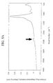
- FIG.4 is a graph showing the examined results.
- an ordinate denotes the amount of moisture (wt%) represented in a linear scale and an abscissa denotes the temperature (°C) represented in a linear scale.
- the amount of moisture in the PE-CVD TMS SiO 2 film 42a is 0.11 wt% whereas the amount of moisture in the PE-CVD TEOS SiO 2 film 51a is 0.49 wt%.
- the amount of moisture in the PE-CVD TMS SiO 2 film 42a is increased merely by +0.2 to 0.3 wt% and thus the amount of moisture is seldom varied.
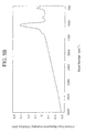
- FIG.5A An ordinate of FIG.5A denotes the absorption intensity expressed in a linear scale (arbitrary unit), and an abscissa denotes the wave number expressed in a linear scale (cm -1 ). Similarly, this is true of FIG.5B.
- the water resistance of the PE-CVD TMS SiO 2 film 42b is exampled by the high pressure humidifying test (pressure-cooker test) while using the samples S2, S3 shown in FIG.2B.
- the similar examination is applied to the comparative sample CS3 employing the PE-CVD TEOS SiO 2 film 51b in place of the PE-CVD TMS SiO 2 film 42b and the comparative sample CS5 employing the PE-CVD SiN film 53 similarly.
- the conditions of the high pressure humidifying test are given as follows.
- the leaving time is used as a parameter.
- FIG.6 is a graph showing the time dependent change of an amount of contained phosphorus in the insulating film after the high pressure humidifying test is carried out.
- the water resistance is examined by another high pressure humidifying test while using the examined sample S3 and the comparative samples CS3, CS4.
- the conditions of the high pressure humidifying test are the same as above.
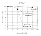
- FIG.7 An ordinate of FIG.7 denotes the water resistance (%) expressed in a linear scale, and an abscissa denotes the leaving time (H (hour)) expressed in a linear scale.
- the sample S3 and the comparative samples CS3, CS4 are used as a parameter.
- the sample S3 has the water resistance of 97.4 % (100 H), that exceeds the comparative samples CS3, CS4.
- the examined sample S1A shown in FIG.2E is formed. That is, the electrode 45 is formed on the PE-CVD TMS SiO 2 film 42 having a film thickness (t) of 200 nm in the sample S1 according to the present invention.
- the leakage current flowing through the silicon substrate 41 and the electrode 45 is measured by applying the voltage between the silicon substrate 41 and the electrode 45.
- the silicon substrate 41 is grounded, and the negative voltage is applied to the electrode 45.
- the leakage current of the PE-CVD TMS SiO 2 film 42a as the single substance is on the order of 10 -8 A/cm 2 at the electric field strength of 5 MV/cm, and the breakdown voltage is about 10 MV/cm in terms of the electric field.
- the insulating film itself of the present invention has essentially the small leakage current like the silicon nitride film, the introduction of the oxygen is not needed to reduce the leakage current, unlike the insulating film containing Si and C.
- the surface of the copper film is oxidized by the introduction of oxygen or the oxygen introducing process and thus the barrier insulating film that comes into contact with the copper film is ready to peel off.
- the adhesiveness between the PE-CVD TMS SiO 2 film 42c according to the present invention and the underlying low dielectric constant insulating film 44a, 44b is examined employing the samples S4, S5. Also, the sample which is subjected to the surface treatment prior to the film formation and the sample which is not subjected to the surface treatment are prepared, and then the similar examination is carried out.
- the surface treatment executed prior to the film formation is the treatment for reforming the surface of the processed film by employing the plasma of N 2 , NH 3 , H 2 , etc.
- the PE-CVD TEOS SiO 2 film 51c is employed in place of the PE-CVD TMS SiO 2 film 42c, and similar examinations are carried out employing the inorganic coating insulating film 44a (the comparative sample CS6) and the organic coating insulating film 44b (the comparative sample CS7)as the low dielectric constant insulating film.
- the peel test by using the tape and the peel test by the CMP (Chemical Mechanical Polishing) on the entire surface of the wafer are carried out.
- the PE-CVD TMS SiO 2 film 42c has the good adhesiveness to the inorganic coating insulating film 44a and the organic coating insulating film 44b.
- a degree of the adhesiveness of the PE-CVD TEOS SiO 2 film 51c is inferior to the PE-CVD TMS SiO 2 film 42c as a whole.
- difference in the adhesiveness appeared in response to whether or not the surface treatment is applied prior to the film formation. That is, the sample which is subjected to the surface treatment prior to the film formation had the higher adhesiveness than the sample which is not subjected to the surface treatment.
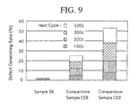
- the defect generating rate due to the heat cycle about the sample S6 and the comparative samples CS8, CS9 is examined. Respective samples are sealed in the package. Test conditions of the heat cycle are given as follows. The cycle number is used as a parameter.
- FIG.9 An ordinate of FIG.9 denotes the defect generating rate (%) expressed in a linear scale, and an abscissa denotes the types of the sample.
- the types of the sample are the sample S6, and the comparative samples CS8, CS9, as explained above, in order from the left side.
- the partition area indicated by a bar graph denotes a fraction defective at a particular cycle number
- the partition area hatched by lateral lines denotes the fraction defective at 100 °C
- the partition area hatched by vertical lines denotes the fraction defective at 200 °C
- the partition area hatched by oblique lines denotes the fraction defective at 300 °C
- the white partition area on a black ground denotes the fraction defective at 500 °C.
- the defect is generated at 300 °C or more, but the defect generating rate is about 2 to 3 % even if the defect generating rates at 300 °C and 500 °C are added.
- the defect is generated almost uniformly from 100 °C to 500 °C, and the defect generating rate is about 25 % in total.
- the defect is generated from 100 °C to 500 °C .
- the defect generating rate at 300 °C and 500 °C are increased, and the defect generating rate is about 53 % in total.
- the TDDB test measures a time required to come up to the dielectric breakdown when the voltage is applied to the sample.
- the examined sample is prepared by stacking the PE-CVD TMS SiO 2 film according to the present invention and the Cu film on the Si substrate in sequence.
- the similar examination is applied to the sample employing the PE-CVD TEOS SiO 2 film in place of the PE-CVD TMS SiO 2 film, and the sample interposing the TiN film between the Cu film and the PE-CVD TEOS SiO 2 film.
- the breakdown lifetime of 10 ⁇ 10 5 seconds is obtained at the electric field strength of 8 MV/cm.
- the electric field strength is 8 MV/cm to get the breakdown lifetime on the order of 10 ⁇ 10 5 seconds. This means that the breakdown lifetime of the sample employing the PE-CVD TMS SiO 2 film is longer by almost six figures than the sample employing the PE-CVD TEOS SiO 2 film.
- the electric field strength is 7.5 MV/cm to get the breakdown lifetime on the order of 10 ⁇ 10 5 seconds.
- the sample employing the PE-CVD TMS SiO 2 film has the longer breakdown lifetime by almost six figures than the sample employing the PE-CVD TEOS SiO 2 film and has the barrier characteristic to Cu, that is equivalent to or more than the TiN film.
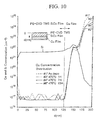
- the examined sample is prepared by stacking the PE-CVD TMS SiO 2 film of 125 nm thickness according to the present invention and the Cu film on the Si substrate (not shown) to contact to each other.
- the examination is made by measuring the Cu concentration distribution state in the PE-CVD TMS SiO 2 film on the basis of the state obtained immediately after the film formation (indicated by a dotted line in FIG.10) after the sample is processed for a predetermined time (three types, i.e., 1 hour (chain double-dashed line), 7 hours (solid line), and 15 hours (dot-dash line)) at the temperature of 470 °C.
- FIG.10 is a graph showing the examined results.
- an ordinate on the left side denotes a Cu concentration and a Si concentration (cm -3 ) represented in a logarithmic scale.
- An abscissa denotes a depth (nm) measured from one surface of the PE-CVD TMS SiO 2 film toward the Cu film side and represented in a linear scale.
- the distribution is seldom changed from the distribution obtained immediately after the film formation. In other words, it is found that the PE-CVD TMS SiO 2 film has the sufficient barrier characteristic to the Cu.
- the alkoxy compound (ex. TMS) having Si-H bonds is employed as the silicon-containing gas in the film forming gas.
- the siloxane having Si-H bonds may be employed.
- N 2 O is employed as the oxygen-containing gas in the above.
- any one selected from the group consisting of oxygen (O 2 ), nitrogen dioxide (NO 2 ), carbon monoxide (CO), carbon dioxide (CO 2 ) and water (H 2 O) may be employed.
- FIGS.11A and 11B Next, a semiconductor device manufacturing method according to a third embodiment of the present invention will be explained with reference to FIGS.11A and 11B hereunder.
- FIG.11A is a sectional view showing a semiconductor device according to the third embodiment of the present invention.
- FIG.11B is a sectional view taken along a I-I line in FIG.11A.
- This semiconductor device is formed of a lower wiring buried insulating film 32 made of an SiOF film with a thickness of approximately 1 m on a base substrate 31.
- a lower wiring recess 32a is formed in the lower wiring buried insulating film 32 and a lower wiring 33 is buried therein.
- an inter-wiring layer insulating film (a protection layer) 34 made of a PE-CVD TMS SiO 2 film (a silicon-containing insulating film) with a thickness of approximately 10 nm according to the present invention, and a upper wiring buried insulating film 35 made of an SiOF film with a thickness of approximately 1 m are laminated in this order.
- the PE-CVD TMS SiO 2 film according to the present invention has a peak of an absorption intensity of an infrared rays in a range of a wave number 2270 to 2350 cm -1 , a film density in a range of 2.25 to 2.40 g/cm 3 , and a relative dielectric constant in a range of 3.3 to 4.3.
- a via-hole 34a is formed in the inter-wiring layer insulating film 34, and an upper wiring recess 35a is formed in the upper wiring buried insulating film 35.
- the upper wiring recess 35a has a larger opening area than the via-hole 34a, and communicates with the via-hole 34a.
- a TaN (a copper diffusion preventing film) 36a and a copper film 36b are buried in the via-hole 34a and the upper wiring recess 35a by the well-known called dual damascene method buries to integrally form a connecting conductor 36 and an upper wiring 37.
- An entire upper most surface thereof is covered with an upper most protection film 38 made of a PE-CVD TMS SiO 2 film according to the present invention.
- the PE-CVD TMS SiO 2 film having the aforementioned characteristics has a high mechanical strength, is dense, has a high water resistance, and has a small content of moisture similarly to a silicon nitride film, and is a lower relative dielectric constant than the silicon nitride.
- the inter-wiring layer insulating film 34 made of the PE-CVD TMS SiO 2 film having the aforementioned characteristics is formed so as to cover the copper film 33b of the upper wiring 33 while contacting the copper film 33b.
- the upper most protection layer 38 is formed so as to cover the copper film 36b of the upper wiring 37 while contacting the copper film 36b.
- the semiconductor device keeps the relative dielectric constant lower, while it can prevent the copper from diffusing from the lower wiring 33 and the upper wiring 37 to a periphery thereof without a barrier insulating film such as a silicon nitride.
- the lower wiring buried insulating film 32 is covered with the inter-wiring layer insulating film 34
- the upper wiring buried insulating film 35 is covered in both a lower surface and an upper surface thereof with the inter-wiring layer insulating film 34 and the upper most protection layer 38. accordingly, a penetration of an incoming moisture to the wiring buried insulating film 32, 35 can be blocked, so that a relative dielectric constant of the wiring buried insulating film 32, 35 can be prevented from changing due to absorption of moisture.
- the lower wiring 33 is covered with the inter-wiring layer insulating film 34 and the upper wiring 37 is covered with the upper most protection layer 38, a corrosion of the wirings 33, 37 can be prevented.
- TMS+N 2 O is employed as the film forming gas for an inter-wiring layer insulating film 34 that is put between a lower wiring-buried insulating film 32 into which a lower wiring 33 is buried and an upper wiring-buried insulating film 35 into which an upper wiring 37 is buried.
- the wiring-buried insulating film 32 formed of an SiOF film having a film thickness of about 1 ⁇ m is formed on a silicon substrate (substrate) 31.
- a wiring recess 32a is formed by etching the wiring-buried insulating film 32, and then a TaN film 33a is formed as a copper diffusion preventing film on an inner surface of the wiring recess 32a.
- a copper seed layer (not shown) is formed on a surface of the TaN film 33a by the sputter method, and then a copper film is buried therein by the plating method.
- the copper film 33b and the TaN film 33a are projected from the wiring recess, are polished by the CMP (Chemical Mechanical Polishing) method to planarize its surface. Accordingly, the lower wiring 33 consisting of the copper wiring 33b and the TaN film 33a is formed. These elements constitute a substrate 20.
- the inter-wiring layer insulating film 34 made of the PE-CVD TMS SiO 2 film having a film thickness of several tens nm is formed by the plasma CVD method using TMS+N 2 O. The details thereof will be explained hereunder.
- the substrate 20 is loaded into the chamber 1 of the plasma film forming equipment 101, and then held by the substrate holder 3. Then, the substrate 20 is heated to be held at the temperature of 350 °C. TMS and the N 2 O gas are introduced into the chamber 1 of the plasma film forming equipment 101 shown in FIG.1 at flow rates of 100 sccm and 3000 sccm respectively to hold the pressure at 0.7 Torr. Then, the power 0.3 W/cm 2 having the frequency of 380 kHz is applied to the lower electrode 3, and also the power 0.3 W/cm 2 having the frequency of 13.56 MHz is applied to the upper electrode 2.
- the inter- wiring layer insulating film 34 made of the PE-CVD TMS SiO 2 film 22 of several tens nm thickness is formed while holding this condition for a predetermined time. According to the examination, the formed PE-CVD TMS SiO 2 film constituting the inter-wiring layer insulating film 34 has the relative dielectric constant of about 3.9 that is measured at the frequency of 1 MHz, and the leakage current of 10 -8 A/cm 2 at the electric field strength of 5 MV/cm.
- the wiring-buried insulating film 35 made of an SiOF film having a film thickness of about 1 ⁇ m is formed on the inter- wiring layer insulating film 34 by the same method that is used to form the SiOF film 32.
- the connecting conductor 36 and the upper wiring 37 made mainly of a copper film 36b are formed by the well-known dual damascene method.
- Various methods are known as the dual damascene method, and then an example will be explained in detail herein.
- a resist film (not shown) is formed on the wiring-buried insulating film 35, and then an opening portion of the resist film is formed in the via-hole forming area by the photolithography method. Then, the wiring- buried insulating film 35 and the inter-wiring layer insulating film 34 are etched via the opening portion of the resist film to pass through. As a result, the via hole 34a is formed in the inter-wiring layer insulating film 34.
- the wiring-buried insulating film 35 is etched via the opening portion of the resist film to pass through.
- the underlying inter-wiring layer insulating film 34 has the etching resistance to the etching gas for the wiring-buried insulating film 35, the etching is stopped by the inter-wiring layer insulating film 34.
- the wiring recess 35a that is connected to the via-hole 34a is formed in the wiring-buried insulating film 35.
- TaN films 36a are formed on inner surfaces of the via-hole 34a and the wiring recess 35a like the above, then a copper seed layer is formed by the sputter method, and then the connecting conductor 36 and the upper wiring 37 are formed by filling a copper film 36b therein.
- the above procedures are the so-called dual damascene method.
- a protection layer 38 is formed on the overall surface by the film forming method to which the present invention is applied. Accordingly, the semiconductor device is completed.
- the PE-CVD TMS SiO 2 film serving as the inter-wiring layer insulating film 34 is formed by plasmanizing the film forming gas, that consists of TMS as the alkoxy compound having Si-H bonds and N 2 O as the oxygen-containing gas, to react.
- the PE-CVD TMS SiO 2 film according to the present invention has the relative dielectric constant of about 3.9 and has the denseness equivalent to the silicon nitride film. Therefore, the effective dielectric constant of the overall insulating film between the wirings can be reduced not to lower the function as the protection layer, i.e., while maintaining the high barrier characteristic to the copper and the small leakage current.
- FIGS.12A and 12B are sectional views showing a multi-layered wiring structure according to a comparative example.
- an inter-wiring layer insulating film 39 in which a silicon oxide film 39b having a film thickness of about 1 ⁇ m is sandwiched by silicon nitride films 39a, 39c each having a film thickness of several tens nm is employed in place of the inter-wiring layer insulating film 34 made of the PE-CVD TMS SiO 2 film, to which the present invention is applied, and that a silicon nitride film 40 having a film thickness of several tens nm is employed in place of the protection layer 38 made of the PE-CVD TMS SiO 2 film.
- the silicon nitride films 39a, 39c, 40 each having the high relative dielectric constant such as about 7.2 are employed, the dielectric constant of the overall insulating film between the wirings becomes high.
- the elements indicated by the same references as those in FIGS.11A and 11B denote the same elements as those in FIGS.11A and 11B, and their explanation will be omitted.
- the diffusion of copper from the copper wirings 33, 37 can be blocked without the barrier insulating film like a silicon nitride, and the lower dielectric constant of the overall insulating film between the wirings can be achieved.
- the inter-wiring layer insulating film 34 made of the PE-CVD TMS SiO 2 film is interposed between the lower wiring-buried insulating film 32 and the upper wiring-buried insulating film 35 that are formed of the SiOF film, and also the upper most protection layer 38 made of the PE-CVD TMS SiO 2 film is formed to cover the upper wiring-buried insulating film 35. Therefore, the diffusion of the fluorine (F) element into the peripheral portions can be prevented by the inter-wiring layer insulating film 34 and the upper most protection layer 38. As a result, the reliability of the wirings can be improved.
- the inter-wiring layer insulating film 34 is formed to cover the lower wiring 33 formed mainly of the copper film 33a and the upper most protection layer 38 is formed to cover the upper wiring 37 formed mainly of the copper film 36a, the diffusion of the copper into the peripheral portions can be prevented
- the leakage current of the insulating film itself of the present invention is essentially small like the silicon nitride film, the introduction of the oxygen is not required to reduce the leakage current, unlike the insulating film containing Si and C. Accordingly, there is no possibility such that surfaces of the copper films 33b, 37b of the upper and lower wirings 33, 37 are oxidized by the introduced oxygen or by the oxygen introducing process and thus the inter-wiring layer insulating film 34 and the barrier insulating film 38 which come into contact with the copper films 33b, 37b are ready to peel off.
- the coating insulating film that is formed by the coating liquid containing the silicon-containing inorganic compound or the silicon-containing organic compound may be employed as the wiring-buried insulating films 32, 35.
- the PE-CVD TMS SiO 2 film serving as the inter-wiring layer insulating films 34, or the protection layer 38 has the good adhesiveness to the coating insulating film, the peeling-off of the film can be prevented and also the discharge of the moisture from the coating insulating film to the peripheral portions can be prevented more completely.
- FIGS.13A to 13G Next, a semiconductor device and a semiconductor device manufacturing method according to a fourth embodiment of the present invention will be explained with reference to FIGS.13A to 13G hereunder.
- FIGS.13G are sectional views showing the semiconductor device according to the fourth embodiment of the present invention.
- this semiconductor device is provided with a lower wiring-buried insulating film 62 on a base substrate 61.
- the lower wiring-buried insulating film 62 is formed by laminating a main insulating film 62a and a first upper protection layer 63a made of the PE-CVD SiO 2 film with a thickness of approximately 50 nm.
- a lower wiring 65 consisting of a TaN film 65a as a copper diffusion preventing film and a copper film 65b are buried in lower wiring recess 64 piercing the lower wiring-buried insulating film 62.
- a semiconductor substrate, the other conductive layer or an insulating substrate may be employed as the base substrate 61.
- This semiconductor device is provided on the aforementioned elements with an inter-wiring layer insulating film 66 having a via-hole 68 and an upper wiring-buried insulating film 67 burying an upper wiring 71 in wiring recess 69.
- the inter-wiring layer insulating film 66 is constituted by a second lower protection layer 66a made of the PE-CVD SiO 2 film of the present invention with a thickness of approximately 50 nm, a main insulating film 66b, and a second upper protection layer 66c made of the PE-CVD SiO 2 film of the present invention with a thickness of approximately 50 nm.
- the upper wiring-buried insulating film 67 is constituted by a main insulating film 67a and a third upper protection layer 67b made of the PE-CVD SiO 2 film of the present invention with a thickness of approximately 50 nm.
- the upper wiring recess 69 has a larger opening area than the via-hole 68, and is formed to connect to the via-hole 68.
- a connecting conductor 70 consisting of a TaN film 70a as a copper diffusion preventing film and a copper film 70b
- an upper wiring 71 consisting of a TaN film 70a as a copper diffusion preventing film and a copper film 70b.
- an entire uppermost surface is covered with an uppermost protection layer 72 made of the PE-CVD SiO 2 film of the present invention.
- a SiOF film or a porous insulating film having a lower dielectric constant may be employed as the above main insulating film 62a, 66b, 67a.
- the PE-CVD TMS SiO 2 film according to the present invention has a peak of an absorption intensity of an infrared rays in a range of a wave number 2270 to 2350 cm -1 , a film density in a range of 2.25 to 2.40 g/cm 3 , and a relative dielectric constant in a range of 3.3 to 4.3.
- the PE-CVD TMS SiO 2 film having the aforementioned characteristics has a high mechanical strength, is dense, has a high water resistance, and has a small content of moisture similarly to a silicon nitride film, and is a lower relative dielectric constant than the silicon nitride.
- the main insulating film 62a of the lower wiring-buried insulating film 62 is covered with the protection layer 63a made of the PE-CVD TMS SiO 2 film having the aforementioned characteristics, and the main insulating film 66b, 67a are covered with the protection layer 66a, 66c, and the protection layer 66c, 67b made of the PE-CVD TMS SiO 2 film having the aforementioned characteristics, respectively. Therefore, the protection layer 66a, 66c, 67b can prevent an incoming moisture from penetrating into the main insulating film 63a, 66b, 67a, and can prevent a relative dielectric constant of the main insulating film 63a, 66b, 67a from changing. Further, since the protection layer 66a, 66c, 67b can prevent the moisture from penetrating into the interior of the semicondutor, a corrosion of the wiring 65, 71 can be prevented.
- the protection layer 63a, 66a, 66c, 67b is formed of not a silicon nitride film but the PE-CVD TMS SiO 2 film having a lower relative dielectric constant, an overall insulating film interposed between the wiring 65, 71 can be reduced in a dielectric constant.
- the protection layer 66a made of the PE-CVD TMS SiO 2 film having the aforementioned characteristics is formed to cover the lower wiring 65, particularly the copper film 65b
- the uppermost protection layer 72 made of the PE-CVD TMS SiO 2 film having the aforementioned characteristics is formed to cover the upper wiring 71, particularly the copper film 70b. Therefore, the protection layer 66a, 72 can prevent the copper from diffusing from the wiring 65, 71 made mainly of the copper film 65b, 70b to the periphery thereof.
- FIGS.13A to 13G are sectional views showing the semiconductor device manufacturing method according to the fourth embodiment of the present invention.
- TMS+N 2 O is used as the film forming gas for the protection layers 63a, 66a, 66c, 67b, 72.
- an underlying insulating film 62a made of the thermal oxide film, the BPSG film, or the like is formed on a base substrate 61, and then a PE-CVD TMS SiO 2 film 63a having a film thickness of about 50 nm is formed by the plasma CVD method using TMS+N 2 O as the film forming gas.
- the formed PE-CVD TMS SiO 2 film 63a has the relative dielectric constant of about 3.9 that is measured at the frequency of 1 MHz, and the leakage current of 10 -8 A/cm 2 at the electric field strength of 5 MV/cm.
- wiring recesses 64 are formed by patterning the PE-CVD TMS SiO 2 film 63a and the underlying insulating film 62a.
- a PE-CVD TMS SiO 2 film 63a acts as the protection layer.
- a TaN film 65a is formed as a copper diffusion preventing film on inner surfaces of the wiring recesses 64.
- a copper seed layer (not shown) is formed and then a copper film 65b is filled to form a lower wiring 65 consisting of the TaN film 65a and the copper film 65b.
- a barrier insulating film 66a made of the PE-CVD TMS SiO 2 film of the present invention to cover the lower wiring 65 is formed, and then an insulating film 66b as a main body of the inter-wiring layer insulating film 66 and a protection layer 66c made of the PE-CVD TMS SiO 2 film of the present invention are formed, whereby an inter-wiring layer insulating film 66 into which the connecting conductor is to be buried is formed.
- a main insulating film 67a of the wiring-buried insulating film and a protection layer 67b made of the PE-CVD TMS SiO 2 film of the present invention are formed on the protection layer 66c in the same manner, whereby a wiring-buried insulating film 67 into which the upper wiring is to be buried is formed.
- the SiOF film having the low dielectric constant is employed as the main insulating film 66b of the inter-wiring layer insulating film 66 and the main insulating film 67a of the wiring-buried insulating film 67, similarly to in the third embodiment.
- a connecting conductor 70 and an upper wiring 71 are formed by the well- known dual damascene method.
- the dual damascene method will be explained in detail hereunder.
- a resist film (not shown) is formed on the protection layer 67b, and then opening portions are formed in the via-hole forming areas of the resist film by the photolithography method. Then, the protection insulating film 67b, the main insulating film 67a, the protection layer 66c, and the main insulating film 66b are etched via the opening portions in the resist film to pierce them. As a result, opening portions 68 are formed in the protection insulating film 66c and the main insulating film 66b of the inter-wiring layer insulating film 66.
- via holes 68 are formed by etching the protection layer 66a to pierce the protection layer 66a.
- the lower wiring 65 is exposed from bottom portions of the via holes 68 and thus the lower wiring 65 and the wiring recesses 69 are connected mutually via the via holes 68.
- TaN films 70a are formed on inner surfaces of the via holes 68 and the wiring recesses 69, then a copper seed layer (not shown) is formed, and then copper films 70b are filled thereon, whereby a connecting conductor 70 and an upper wiring 71 are formed.
- a copper seed layer (not shown) is formed, and then copper films 70b are filled thereon, whereby a connecting conductor 70 and an upper wiring 71 are formed.
- a protection layer 72 made of the PE-CVD TMS SiO 2 film is formed on the entire surface by the film forming method to which the present invention is applied.
- the method is performed to form the inter-wiring layer insulating film 66 and the wiring-buried insulating film 67 by laminating sequentially the insulating film and the protection layer from the bottom, and then to pass through the protection layer, the inter-wiring layer insulating film 66 and the wiring-buried insulating film 67 such that their opening areas are expanded sequentially from the lower side respectively so as to form alternatively the via holes 68 and the wiring recesses 69 connected to the via holes 68.
- the protection layer 66c acts as the underlying film of the main insulating film 67a that is etched to selectively etch the insulating film 67a. Since the protection layer 66c to which the present invention is applied is dense, such film can effectively function as the mask or such film can effectively function as the stopper to prevent the excessive etching of the underlying insulating film 66b.
- the coating insulating film having the low dielectric constant may be employed as the main insulating films 66b, 67a in place of the SiOF film.
- FIG.14 is a sectional view showing the semiconductor device according to the fifth embodiment of the present invention.
- the semiconductor device according to this embodiment is provided with a laminated structure which is formed by laminating sequentially an inter-wiring layer insulating film 82, a wiring-buried insulating film 83, an inter-wiring layer insulating film 84, a wiring-buried insulating film 85, an inter-wiring layer insulating film 86, and a wiring-buried insulating film 87 on a substrate 81 from the bottom.
- the PE-CVD TMS SiO 2 film according to the present invention has a peak of an absorption intensity of an infrared rays in a range of a wave number 2270 to 2350 cm -1 , a film density in a range of 2.25 to 2.40 g/cm 3 , and a relative dielectric constant in a range of 3.3 to 4.3.
- the above SiOF film or the above coating insulating film may be employed as the insulating films 82a/82c, 83a/83c, 84a/84c, 85a/85c, 86a/86c, 87a formed of the low dielectric constant insulating film.
- the inter-wiring layer insulating films 82, 84, 86 are formed by laminating the main insulating films 82a/82c, 84a/84c, 86a/86c and the protection layers 82d, 84d, 86d sequentially from the bottom.
- the wiring-buried insulating films 83, 85, 87 are formed by laminating the main insulating films 83a/83c, 85a/85c, 87a and the protection layers 83d, 85d, 87b sequentially from the bottom.
- the insulating films (the protection layer) 82b, 84b, 86b made of the PE-CVD TMS SiO 2 film of the present invention are interposed between the main insulating films 82a/82c, 84a/84c, 86a/86c of the inter-wiring layer insulating films 82, 84, 86 respectively, and also the insulating films (the protection layer) 83b, 85b made of the PE-CVD TMS SiO 2 film of the present invention are interposed between the main insulating films 83a/83c, 85a/85c of the wiring-buried insulating films 83, 85.
- the insulating films 82b, 84b, 86b and the insulating films 83b, 85b are interposed to prevent such cracks.
- the via holes 88a, 88c, 88e are formed in the inter-wiring layer insulating films 82, 84, 86, and the wiring recesses 88b, 88d, 88f are formed in the wiring-buried insulating films 83, 85, 87. That is, the via holes 88a, 88c, 88e and the wiring recesses 88b, 88d, 88f are formed alternatively such that their opening areas are expanded sequentially from the lower side and that the via holes 88a, 88c, 88e and the neighboring wiring recesses 88b, 88d, 88f are connected mutually.
- a copper diffusion preventing film 89a made of a TaN film is formed on inner surfaces of the via holes 88a, 88c, 88e and the wiring recesses 88b, 88d, 88f, and then a copper film 89b is buried therein via the copper diffusion preventing film 89a.
- the copper diffusion preventing film 89a and the copper film 89b buried in the via holes 88a, 88c, 88e act as the connecting conductor for connecting the upper and lower wirings respectively.
- the copper diffusion preventing film 89a and the copper film 89b buried in the wiring recesses 88b, 88d, 88f constitutes the wiring respectively.
- the structure constructed by burying the wiring formed of the copper film or formed mainly of the copper film in the wiring-buried insulating film like the substrate 21 in FIG.13D, for example, may be employed as the substrate 81.
- this wiring is connected to the connecting conductor 89 in the via hole 88a formed in the protection layer covering the wiring as well.
- the multi-layered wiring has three layers in the number of layers and its number is more than that of the fourth embodiment, the same advantages as the fourth embodiment are obtained.
- the manufacturing method explained in the fourth embodiment may be employed as the above semiconductor device manufacturing method. Such manufacturing method will be explained in brief hereunder.
- TMS+N 2 O is employed as a film forming gas of the protection layers 82d, 83d, 84d, 85d, 86d, 87d and the insulating films 82b, 83b, 84b, 85b, 86b.
- the low dielectric constant insulating films 82a, 82c, 83a, 83c, 84a, 84c, 85a, 85c, 86a,86c, 87a (referred to as "82a to 87a” hereinafter) and the insulating films 82b, 82d, 83b,83d, 84b, 84d, 85b, 85d, 86b, 86d, 87b made of the PE-CVD TMS SiO 2 film (referred to as "82b to 87b” hereinafter) are formed alternatively from the lower side on the substrate 81.
- the insulating films 82a to 82d are referred to as the inter-wiring layer insulating film 82, the insulating films 83a to 83d are referred to as the inter-wiring layer insulating film 83, the insulating films 84a to 84d are referred to as the inter-wiring layer insulating film 84, the insulating films 85a to 85d are referred to as the inter-wiring layer insulating film 85, the insulating films 86a to 86d are referred to as the inter-wiring layer insulating film 86, and the insulating films 87a and 87b are referred to as the inter-wiring layer insulating film 87.
- the inter-wiring layer insulating film 82, etc. and the wirng-buried insulating film 83, etc. are constituted by at least two sets as a set consisting of the insulating film 82a to 87a as a lower layer and the protection layer 82b to 87b as a upper layer.
- opening portions 88a to 88f are formed in the inter-wiring layer insulating films 82, etc. and the wiring-buried insulating films 83, etc., which are laminated alternatively, to pass through such that their opening areas are expanded sequentially and that they are connected mutually.
- These opening portions 88a to 88f serve as the via holes 88a, 88c, 88e and the wiring recesses 88b, 88d, 88f connected to these via holes.
- the connecting conductors and the wirings 89a, 89b are formed such that the wirings in the upper and lower wiring recesses 88b, 88d, 88f are connected via the connecting conductors formed in the via holes 88a, 88c, 88e.
- the protection layer 90 formed of the PE-CVD TMS SiO 2 film of the present invention is formed, whereby the semiconductor device is completed.
- the number of layers in the multi-layered wiring i.e., three layers, is larger than the fourth embodiment, nevertheless the advantages similar to the fourth embodiment can be achieved.
- the silicon-containing insulating film according to the present invention has a peak of an absorption intensity of an infrared rays in a range of a wave number 2270 to 2350 cm -1 , a film density in a range of 2.25 to 2.40 g/cm 3 , and a relative dielectric constant in a range of 3.3 to 4.3.
- the semiconductor device of the present invention has a protection layer covering a wiring made only or mainly of a copper film, and the protection layer is formed of the silicon-containing insulating film having the aforementioned characteristics. Accordingly, since the protection layer is dense similarly to a silicon nitride, it can prevent the copper from diffusing to a periphery of the wiring.
- an inter-wiring layer insulating film having the aforementioned characteristics is interposed between the lower wiring and the upper wiring. Therefore, the inter-wiring layer insulating film can prevent the copper from diffusing from the wiring to a periphery thereof, while the semiconductor device maintains a lower dielectric constant.
- the semiconductor device has a main insulating film, protection layers covering it in both a lower surface and an upper surface.
- the protection layers having the aforementioned characteristics are interposed both between the lower wiring and the main insulating film and between the upper wiring and the main insulating film, respectively. Therefore, the protection layers can prevent the copper from diffusing from the wirings to the main insulating film.
- a porous insulating film or a coating insulating film having a lower dielectric constant as the main insulating film results in preventing the copper from diffusing to the main insulating film from the wirings while maintaining a lower dielectric constant.
- the silicon-containing insulating film is formed by plasmanizing the film forming gas, that consists of any one selected from the group consisting of the alkoxy compound having Si-H bonds and the siloxane having Si-H bonds and any one oxygen-containing gas selected from the group consisting of O 2 , N 2 O, NO 2 , CO, CO 2 , and H 2 O, to react.
- the silicon-containing insulating film formed by the above film-forming condition is dense, is excellent in the water resistance, has the small amount of contained moisture in the film, and has the small relative dielectric constant.
- the inter-wiring layer insulating film is put between the lower wiring-buried insulating film into which the lower wiring formed only or mainly of the copper film is buried and the upper wiring-buried insulating film into which the upper wiring formed only or mainly of the copper film is buried, if the silicon-containing insulating film formed by the above film-forming condition is formed as the inter-wiring layer insulating film, the diffusion of the copper from the lower wiring and the upper wiring can be prevented without the barrier insulating film and also the lower dielectric constant can be achieved in the overall insulating film between the wirings.
- the main insulating films and the protection layers made of the silicon-containing insulating film of the present invention are laminated alternatively to form a multi-layered structure with the inter-wiring layer insulating films and the wiring-buried insulating films laminated alternatively two layers or more. Then, the via holes and the wiring recesses are formed in the inter-wiring layer insulating films and the wiring-buried insulating films, and then the connecting conductor and the wiring are buried in the via holes and the wiring recesses. Therefore, since the protection layer is interposed between the wiring and the main insulating film, the diffusion of the copper from the copper wirings into the main insulating film can be prevented.
- the lower wiring is covered with the protection layer made of the silicon-containing insulating film of the present invention, the diffusion of the copper into the peripheral portions can be prevented.
- the insulating film itself of the present invention has essentially the small leakage current like the silicon nitride film, the introduction of the oxygen is not needed to reduce the leakage current, unlike the insulating film containing Si and C. Therefore, there is no possibility that a peeling-off of the protection layer, etc. that contacts to the wiring is caused by the introduced oxygen or the oxygen introducing process.
- the insulating film having the low relative dielectric constant is employed not to employ the silicon nitride film as the protection layer, the insulating film between the wirings as a whole can be reduced in the dielectric constant.
Applications Claiming Priority (4)
| Application Number | Priority Date | Filing Date | Title |
|---|---|---|---|
| JP2000221381 | 2000-07-21 | ||
| JP2000221381 | 2000-07-21 | ||
| JP2000281263 | 2000-09-18 | ||
| JP2000281263 | 2000-09-18 |
Publications (2)
| Publication Number | Publication Date |
|---|---|
| EP1174916A2 true EP1174916A2 (fr) | 2002-01-23 |
| EP1174916A3 EP1174916A3 (fr) | 2003-09-10 |
Family
ID=26596474
Family Applications (1)
| Application Number | Title | Priority Date | Filing Date |
|---|---|---|---|
| EP01116695A Withdrawn EP1174916A3 (fr) | 2000-07-21 | 2001-07-17 | Dispositif semiconducteur et méthode de fabrication |
Country Status (4)
| Country | Link |
|---|---|
| US (1) | US6500752B2 (fr) |
| EP (1) | EP1174916A3 (fr) |
| KR (1) | KR100399633B1 (fr) |
| TW (1) | TW502405B (fr) |
Cited By (3)
| Publication number | Priority date | Publication date | Assignee | Title |
|---|---|---|---|---|
| US6835669B2 (en) | 2000-07-21 | 2004-12-28 | Canon Sales Co., Inc. | Film forming method, semiconductor device and semiconductor device manufacturing method |
| US7686154B2 (en) | 2006-02-09 | 2010-03-30 | Smiths Heimann Gmbh | Inspection station for screening hand luggage and other items carried by persons |
| CN104911563A (zh) * | 2015-06-29 | 2015-09-16 | 聚灿光电科技股份有限公司 | Cvd设备及cvd设备保护层形成方法 |
Families Citing this family (13)
| Publication number | Priority date | Publication date | Assignee | Title |
|---|---|---|---|---|
| US7122900B2 (en) * | 2000-06-26 | 2006-10-17 | Renesas Technology Corp. | Semiconductor device and method manufacturing the same |
| KR100486333B1 (ko) * | 2000-07-21 | 2005-04-29 | 가부시끼가이샤 한도따이 프로세스 켄큐쇼 | 반도체 장치 및 그 제조 방법 |
| CA2454871C (fr) * | 2001-07-26 | 2008-09-30 | Alveolus Inc | Endoprothese amovible et procede d'utilisation associe |
| JP2003258085A (ja) * | 2002-02-27 | 2003-09-12 | Fujitsu Ltd | 配線構造及びその形成方法 |
| TWI278962B (en) * | 2002-04-12 | 2007-04-11 | Hitachi Ltd | Semiconductor device |
| US6621167B1 (en) * | 2002-09-23 | 2003-09-16 | United Microelectronics Corp. | Metal interconnect structure |
| JP2005294333A (ja) * | 2004-03-31 | 2005-10-20 | Semiconductor Process Laboratory Co Ltd | 成膜方法及び半導体装置 |
| JP5180426B2 (ja) | 2005-03-11 | 2013-04-10 | ルネサスエレクトロニクス株式会社 | 半導体装置の製造方法 |
| JP4578332B2 (ja) * | 2005-06-15 | 2010-11-10 | ルネサスエレクトロニクス株式会社 | 半導体装置およびその製造方法 |
| JP2007059705A (ja) * | 2005-08-25 | 2007-03-08 | Seiko Epson Corp | キャパシタおよびその製造方法、強誘電体メモリ装置の製造方法、アクチュエータの製造方法、並びに、液体噴射ヘッドの製造方法 |
| WO2008094845A2 (fr) * | 2007-02-01 | 2008-08-07 | Willard & Kelsey Solar Group, Llc | Système et procédé de revêtement de semi-conducteur sur une feuille de verre et produit obtenu |
| US7998801B2 (en) | 2008-04-25 | 2011-08-16 | Semiconductor Energy Laboratory Co., Ltd. | Manufacturing method of thin film transistor having altered semiconductor layer |
| US10475930B2 (en) * | 2016-08-17 | 2019-11-12 | Samsung Electronics Co., Ltd. | Method of forming crystalline oxides on III-V materials |
Citations (4)
| Publication number | Priority date | Publication date | Assignee | Title |
|---|---|---|---|---|
| US5491108A (en) * | 1993-06-08 | 1996-02-13 | Nec Corporation | Method of producing semiconductor integrated circuit device having interplayer insulating film covering substrate |
| EP0845804A2 (fr) * | 1996-11-29 | 1998-06-03 | Canon Sales Co., Inc. | Prétraitement d'un substrat avant le dépÔt d'une couche isolante |
| WO1999041423A2 (fr) * | 1998-02-11 | 1999-08-19 | Applied Materials, Inc. | Traitements au plasma pour depot de films a faible constante dielectrique |
| EP0851480B1 (fr) * | 1996-12-25 | 2001-10-31 | Canon Sales Co., Inc. | Procédé de fabrication d'un film isolant à tension réglée, dispositif semiconducteur et son procédé de fabrication |
Family Cites Families (6)
| Publication number | Priority date | Publication date | Assignee | Title |
|---|---|---|---|---|
| AU7371898A (en) | 1997-05-07 | 1998-11-27 | Mark J. Hampden-Smith | Low density film for low dielectric constant applications |
| EP0881678A3 (fr) | 1997-05-28 | 2000-12-13 | Texas Instruments Incorporated | Améliorations dans ou relatives à des structures diélectriques poreuses |
| US5976979A (en) * | 1997-06-10 | 1999-11-02 | Industrial Technology Research Institute | Sequential oxygen plasma treatment and chemical mechanical polish (CMP) planarizing method for forming planarized low dielectric constant dielectric layer |
| JP3390329B2 (ja) * | 1997-06-27 | 2003-03-24 | 日本電気株式会社 | 半導体装置およびその製造方法 |
| JP3726226B2 (ja) | 1998-02-05 | 2005-12-14 | 日本エー・エス・エム株式会社 | 絶縁膜及びその製造方法 |
| JP3615979B2 (ja) * | 2000-01-18 | 2005-02-02 | 株式会社ルネサステクノロジ | 半導体装置及びその製造方法 |
-
2001
- 2001-07-16 US US09/904,869 patent/US6500752B2/en not_active Expired - Fee Related
- 2001-07-17 EP EP01116695A patent/EP1174916A3/fr not_active Withdrawn
- 2001-07-18 TW TW090117528A patent/TW502405B/zh not_active IP Right Cessation
- 2001-07-19 KR KR10-2001-0043415A patent/KR100399633B1/ko not_active IP Right Cessation
Patent Citations (4)
| Publication number | Priority date | Publication date | Assignee | Title |
|---|---|---|---|---|
| US5491108A (en) * | 1993-06-08 | 1996-02-13 | Nec Corporation | Method of producing semiconductor integrated circuit device having interplayer insulating film covering substrate |
| EP0845804A2 (fr) * | 1996-11-29 | 1998-06-03 | Canon Sales Co., Inc. | Prétraitement d'un substrat avant le dépÔt d'une couche isolante |
| EP0851480B1 (fr) * | 1996-12-25 | 2001-10-31 | Canon Sales Co., Inc. | Procédé de fabrication d'un film isolant à tension réglée, dispositif semiconducteur et son procédé de fabrication |
| WO1999041423A2 (fr) * | 1998-02-11 | 1999-08-19 | Applied Materials, Inc. | Traitements au plasma pour depot de films a faible constante dielectrique |
Non-Patent Citations (1)
| Title |
|---|
| BOGART K H A ET AL: "PLASMA ENHANCED CHEMICAL VAPOR DEPOSITION OF SIO2 USING NOVEL ALKOXYSILANE PRECURSORS" JOURNAL OF VACUUM SCIENCE AND TECHNOLOGY: PART A, AMERICAN INSTITUTE OF PHYSICS. NEW YORK, US, vol. 13, no. 2, 1 March 1995 (1995-03-01), pages 476-480, XP000498543 ISSN: 0734-2101 * |
Cited By (3)
| Publication number | Priority date | Publication date | Assignee | Title |
|---|---|---|---|---|
| US6835669B2 (en) | 2000-07-21 | 2004-12-28 | Canon Sales Co., Inc. | Film forming method, semiconductor device and semiconductor device manufacturing method |
| US7686154B2 (en) | 2006-02-09 | 2010-03-30 | Smiths Heimann Gmbh | Inspection station for screening hand luggage and other items carried by persons |
| CN104911563A (zh) * | 2015-06-29 | 2015-09-16 | 聚灿光电科技股份有限公司 | Cvd设备及cvd设备保护层形成方法 |
Also Published As
| Publication number | Publication date |
|---|---|
| KR100399633B1 (ko) | 2003-09-29 |
| KR20020009429A (ko) | 2002-02-01 |
| EP1174916A3 (fr) | 2003-09-10 |
| TW502405B (en) | 2002-09-11 |
| US6500752B2 (en) | 2002-12-31 |
| US20020011672A1 (en) | 2002-01-31 |
Similar Documents
| Publication | Publication Date | Title |
|---|---|---|
| US6479409B2 (en) | Fabrication of a semiconductor device with an interlayer insulating film formed from a plasma devoid of an oxidizing agent | |
| JP2002164342A (ja) | 半導体装置及びその製造方法 | |
| EP1174916A2 (fr) | Dispositif semiconducteur et méthode de fabrication | |
| US6911405B2 (en) | Semiconductor device and method of manufacturing the same | |
| KR100484321B1 (ko) | 반도체 장치 및 그 제조 방법 | |
| KR100484322B1 (ko) | 반도체 장치 및 그 제조 방법 | |
| JP3701626B2 (ja) | 半導体装置の製造方法 | |
| US6646327B2 (en) | Semiconductor device and semiconductor device manufacturing method | |
| US6835669B2 (en) | Film forming method, semiconductor device and semiconductor device manufacturing method | |
| KR100746679B1 (ko) | 성막 방법, 반도체 장치의 제조 방법 및 반도체 장치 | |
| JP3934343B2 (ja) | 半導体装置及びその製造方法 | |
| JP3845061B2 (ja) | 半導体装置及びその製造方法 | |
| US20050095828A1 (en) | Process for sealing plasma-damaged, porous low-k materials | |
| JP2004015034A (ja) | 成膜方法、成膜装置及び成膜装置のクリーニング方法 | |
| JP2004228599A (ja) | 半導体装置 | |
| JP2002305242A (ja) | 半導体装置の製造方法 | |
| JP2002164429A (ja) | 半導体装置及びその製造方法 | |
| EP1128421A2 (fr) | Méthode de fabrication d'une d'une couche isolante intermédiaire contenant les éléments Si, C, O et H pour composants semiconducteurs | |
| JP2002164346A (ja) | 成膜方法、半導体装置及びその製造方法 |
Legal Events
| Date | Code | Title | Description |
|---|---|---|---|
| PUAI | Public reference made under article 153(3) epc to a published international application that has entered the european phase |
Free format text: ORIGINAL CODE: 0009012 |
|
| AK | Designated contracting states |
Kind code of ref document: A2 Designated state(s): AT BE CH CY DE DK ES FI FR GB GR IE IT LI LU MC NL PT SE TR |
|
| AX | Request for extension of the european patent |
Free format text: AL;LT;LV;MK;RO;SI |
|
| PUAL | Search report despatched |
Free format text: ORIGINAL CODE: 0009013 |
|
| AK | Designated contracting states |
Kind code of ref document: A3 Designated state(s): AT BE CH CY DE DK ES FI FR GB GR IE IT LI LU MC NL PT SE TR |
|
| AX | Request for extension of the european patent |
Extension state: AL LT LV MK RO SI |
|
| RIC1 | Information provided on ipc code assigned before grant |
Ipc: 7H 01L 23/532 B Ipc: 7C 23C 16/509 B Ipc: 7C 23C 16/40 B Ipc: 7H 01L 21/768 B Ipc: 7H 01L 21/316 A |
|
| AKX | Designation fees paid | ||
| REG | Reference to a national code |
Ref country code: DE Ref legal event code: 8566 |
|
| STAA | Information on the status of an ep patent application or granted ep patent |
Free format text: STATUS: THE APPLICATION IS DEEMED TO BE WITHDRAWN |
|
| 18D | Application deemed to be withdrawn |
Effective date: 20040311 |