EP1126584A2 - Procédé d'élévation de tension courant continu - courant continu et circuit d'alimentation de puissance utilisant le même - Google Patents
Procédé d'élévation de tension courant continu - courant continu et circuit d'alimentation de puissance utilisant le même Download PDFInfo
- Publication number
- EP1126584A2 EP1126584A2 EP01101607A EP01101607A EP1126584A2 EP 1126584 A2 EP1126584 A2 EP 1126584A2 EP 01101607 A EP01101607 A EP 01101607A EP 01101607 A EP01101607 A EP 01101607A EP 1126584 A2 EP1126584 A2 EP 1126584A2
- Authority
- EP
- European Patent Office
- Prior art keywords
- voltage
- circuit
- clock signals
- booster
- frequency
- Prior art date
- Legal status (The legal status is an assumption and is not a legal conclusion. Google has not performed a legal analysis and makes no representation as to the accuracy of the status listed.)
- Withdrawn
Links
Images


Classifications
-
- G—PHYSICS
- G09—EDUCATION; CRYPTOGRAPHY; DISPLAY; ADVERTISING; SEALS
- G09G—ARRANGEMENTS OR CIRCUITS FOR CONTROL OF INDICATING DEVICES USING STATIC MEANS TO PRESENT VARIABLE INFORMATION
- G09G3/00—Control arrangements or circuits, of interest only in connection with visual indicators other than cathode-ray tubes
- G09G3/20—Control arrangements or circuits, of interest only in connection with visual indicators other than cathode-ray tubes for presentation of an assembly of a number of characters, e.g. a page, by composing the assembly by combination of individual elements arranged in a matrix no fixed position being assigned to or needed to be assigned to the individual characters or partial characters
- G09G3/34—Control arrangements or circuits, of interest only in connection with visual indicators other than cathode-ray tubes for presentation of an assembly of a number of characters, e.g. a page, by composing the assembly by combination of individual elements arranged in a matrix no fixed position being assigned to or needed to be assigned to the individual characters or partial characters by control of light from an independent source
- G09G3/36—Control arrangements or circuits, of interest only in connection with visual indicators other than cathode-ray tubes for presentation of an assembly of a number of characters, e.g. a page, by composing the assembly by combination of individual elements arranged in a matrix no fixed position being assigned to or needed to be assigned to the individual characters or partial characters by control of light from an independent source using liquid crystals
-
- H—ELECTRICITY
- H02—GENERATION; CONVERSION OR DISTRIBUTION OF ELECTRIC POWER
- H02M—APPARATUS FOR CONVERSION BETWEEN AC AND AC, BETWEEN AC AND DC, OR BETWEEN DC AND DC, AND FOR USE WITH MAINS OR SIMILAR POWER SUPPLY SYSTEMS; CONVERSION OF DC OR AC INPUT POWER INTO SURGE OUTPUT POWER; CONTROL OR REGULATION THEREOF
- H02M3/00—Conversion of dc power input into dc power output
- H02M3/02—Conversion of dc power input into dc power output without intermediate conversion into ac
- H02M3/04—Conversion of dc power input into dc power output without intermediate conversion into ac by static converters
- H02M3/06—Conversion of dc power input into dc power output without intermediate conversion into ac by static converters using resistors or capacitors, e.g. potential divider
- H02M3/07—Conversion of dc power input into dc power output without intermediate conversion into ac by static converters using resistors or capacitors, e.g. potential divider using capacitors charged and discharged alternately by semiconductor devices with control electrode, e.g. charge pumps
Definitions
- the present invention relates to a DC-DC voltage boosting method and a power supply using the same. More particularly, the present invention relates to a DC-DC voltage boosting method and a power supply circuit of the charge pump type, which are incorporated in a voltage-boost power supply circuit for driving a liquid crystal device, or in a driver IC containing a power supply for driving a liquid crystal device.
- a liquid crystal device requires a high-voltage power supply for driving liquid crystals, and the high-voltage power is generally obtained by DC-DC boosting.
- Fig. 13 shows the configuration of a typical power supply circuit incorporated in a driver IC for driving a liquid crystal device.
- This IC operates by receiving a power supply voltage V DD - V SS (V DD being high potential and V SS low potential, in the following V SS will be considered a reference potential and V DD the power supply voltage relative to the reference potential).
- V DD being high potential and V SS low potential, in the following V SS will be considered a reference potential and V DD the power supply voltage relative to the reference potential).
- V DD being high potential and V SS low potential, in the following V SS will be considered a reference potential and V DD the power supply voltage relative to the reference potential).
- V DD being high potential and V SS low potential, in the following V SS will be considered a reference potential and V DD the power supply voltage relative to the reference potential.
- a voltage booster circuit 10 boosts the power supply voltage V DD .
- the boosted voltage V OUT is fed to a voltage regulator circuit
- Fig. 14 is a circuit diagram showing an example of the configuration of the voltage booster circuit 10, and Fig. 15 shows an example of the configuration of the voltage regulator circuit 20.
- a P-channel transistor Q 1P and an N-channel transistor Q 1N are connected in series between first and second supply voltage terminals to which the potentials V DD and V SS , respectively, are applied.
- a P-channel transistor Q 2P and an N-channel transistor Q 2N are connected in series.
- P-channel transistors Q 3 , Q 4 , and Q 5 are connected in series between the first supply voltage terminal and a terminal from which the boosted voltage V out is taken off.
- a capacitor C 1 is connected between the source of the transistor Q 3 and the drain of both transistors Q 1P and Q 1N
- a capacitor C 2 is connected between the source of the transistor Q 4 and the drain of both transistors Q 2P and Q 2N .
- the boosted voltage V OUT is obtained from the source of the transistor Q 5 .
- Fig 16 is a schematic representation showing wave forms of clock signals which are input to the voltage booster circuit shown in Fig. 14, in the case where the input voltage is tripled.
- a clock signal CL 1P input to the gate of the transistor Q 1P and a clock signal CL 1N input to the gate of the transistor Q 1N are the same.
- a clock signal CL 2P input to the gate of the transistor Q 2P and a clock signal CL 2N input to the gate of the transistor Q 2N are the inverted version (180° phase shifted) of the clock signal of CL 1P and CL 1N .
- the clock signals CL 1P , CL 1N , CL 2P , and CL 2N alternate between potentials V DD and V SS .
- a clock signal CL 3 input to the gate of the transistor Q 3 and a clock signal CL 5 input to the gate of the transistor Q 5 are the inverted version of the clock signals CL 1P and CL 1N .
- a clock signal CL 4 input to the gate of the transistor Q 4 is the inverted version of the clock signals CL 2P and CL 2N .
- the clock signals CL 3 , CL 4 , and CL 5 alternate between the boosted voltage or potential V OUT and the reference potential V SS .
- the clock signals CL 2P and CL 2N are fixed to V DD
- the clock signal CL5 is fixed to V SS .
- a driver IC for driving liquid crystals is of the chip-on-glass (COG) type so that the driver IC is mounted on a glass substrate, it is necessary to reduce electric terminals which connect a printed circuit substrate and a liquid crystal display device. Accordingly, the driver IC for driving liquid crystals is required to contain a charge pump capacitor for boosting a voltage.
- COG chip-on-glass
- Capacitors contained in ICs however, always include a stray capacitance.
- a reactive current due to charging and discharging of the stray capacitance also increases.
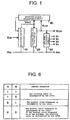
- Fig. 17 shows the stray capacitance.
- a lower electrode 93 of a capacitor is formed over a semiconductor substrate 91 via an insulator film 92, and an upper electrode 95 of the capacitor is formed above the lower electrode 93 via a dielectric material 94. Accordingly, the lower electrode 93 and the semiconductor substrate 91 form a stray capacitance C S between themselves.
- an N + region 96 is formed in the semiconductor substrate 91 so as to be the lower electrode of the capacitor, and the upper electrode 95 is formed above the lower electrode 96 via the dielectric material 94. Accordingly, the lower electrode 96 and the semiconductor substrate 91 forms the stray capacitance C S between themselves.
- Capacitors contained in an IC must be configured such that the stray capacitance is small, and the switching frequency must be adjusted to a necessary and sufficient value.
- the boosted voltage V OUT varies with the output impedance and the load current I OUT of the voltage-boost power supply.
- the output impedance varies with the capacities of capacitors and the switching frequency. Since capacitors contained in an IC are small and the switching frequency is preferably low, the output impedance of the voltage-boost power supply tends to be large.
- the load current I OUT is determined primarily by the current charging and discharging the liquid crystal panel, and this current varies with the display mode and display contents.
- the boosting ratio must be adjusted to a minimum value required for the respective display mode and display contents. According to above-mentioned JP documents, however, only an adjustment of the switching frequency is provided and an adjustment of the boosting ratio is not considered.
- the adjustment of the boosting ratio may be achieved with software control using a microprocessor unit (MPU). In such a case, however, only an adjustment in accordance with the display mode is possible, and an adjustment in accordance with the display contents cannot be achieved.
- MPU microprocessor unit
- an object of the present invention is to provide a DC-DC voltage boosting method and a booster circuit which are capable of cutting down the power consumption even when the display mode or the display content is changed, by detecting a margin of the boosted voltage.
- Another object of the present invention is to provide a layout configuration which provides a low stray capacity and is suitable for an internal switching capacitor of an IC.
- the present invention as defined in the claims is capable of cutting down the power consumption even when the display mode or display content of the liquid crystal panel is changed, by detecting the margin of the boosted voltage and by adjusting the frequency of the clock signals or fixing at least one of the clock signals which control switching components.
- a power supply circuit has the overall configuration shown in Fig. 1.
- Power supply potentials V DD (high potential side) and V SS (low potential side) are applied to this power supply circuit for operation.
- One of these power supply potentials may be earth.
- V SS is set to be equal to earth potential. Therefore, V DD will also be referred to as the power supply voltage (relative to the earth or reference potential V SS ) in the following.
- a booster circuit 10 boosts the power supply voltage V DD and outputs a boosted voltage V OUT .
- a voltage regulator circuit 20 to which the boosted voltage V OUT is supplied makes an operating voltage V LCD for liquid crystal display device.
- a voltage follower circuit 30 divides and buffers the operating voltage V LCD and outputs various voltages V 1 , V 2 , V 3 and V 4 corresponding to the load required for various functions.
- the booster circuit 10 and the voltage regulator circuit 20 may have the same configuration and operation as those shown in Fig. 14 and Fig. 15, respectively. When the booster circuit shown in Fig. 14 carries out triple boosting, the booster clock signals shown in Fig. 16 may be used. When the operating voltage V LCD and the boosted voltage V OUT are set to be equal, there is no need for the voltage regulator circuit 20.
- the power supply circuit of this embodiment further includes a booster clock adjusting circuit 40 (referred to as BCA circuit hereinafter).
- BCA circuit a booster clock adjusting circuit 40
- the boosted voltage V OUT from the booster circuit 10 and the operating voltage V LCD from the voltage regulator circuit 20 are supplied. These voltages are compared so that various adjustments such as gating the booster clock signals supplied to the booster circuit or changing the frequency thereof can be carried out.
- the boosting operation of the booster circuit 10 can be controlled.
- the BCA circuit 40 adjusts the booster clock signals based only on the boosted voltage V OUT .
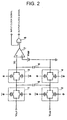
- Fig. 2 shows a configuration example of the BCA circuit 40.
- the BCA circuit includes switching circuits 1 to 4 each having the source-drain paths of a P-channel transistor and an N-channel transistor connected in parallel.
- the switching circuits 1 to 4 are opened/closed in response to control clock signals ⁇ and / ⁇ (/ ⁇ symbolizes the inverted (180° phase-shifted) version of ⁇ shown as "barred" in the drawing).
- the switching circuit 1 is closed when the control clock signal ⁇ is at high level and the control clock signal / ⁇ is at low level, and is opened when the control clock signal ⁇ is at low level and the control clock signal / ⁇ is at high level.
- the voltage difference (actual margin voltage) between the boosted voltage V OUT and the operating voltage V LCD is supplied to a capacitor 5 when the switching circuits 1 and 2 are closed and when the switching circuits 3 and 4 are opened.
- the voltage across the two ends of the capacitor 5 is supplied to a capacitor 6 when the switching circuits 3 and 4 are closed and the switching circuits 1 and 2 are opened.
- the voltage V C between the two ends of the capacitor 6 is applied to a comparator 7.
- the comparator 7 compares this voltage V C with a predetermined voltage V REF to output a comparison result to at least one gate circuit 8. It will be noted that an A/D converter may be used as a circuit for comparing these voltages, instead of the comparator 7.
- the gate circuit 8 is implemented by an OR circuit.
- the predetermined voltage V REF is set to be equal to the desired margin voltage between the boosted voltage V OUT and the operating voltage V LCD .
- the OR circuit 8 outputs a booster clock signal that is supplied to the OR circuit 8.
- This booster clock signal is supplied, for example, as a booster clock signal CL 2P to the gate of the P-channel transistor Q 2P in the booster circuit shown in Fig. 14.
- the OR circuit 8 supplies a high-level signal, rather than the booster clock signal, to the booster circuit. This makes it possible to change the boosting ratio of the booster circuit, so that the voltage difference between the boosted voltage V OUT and the operating voltage V LCD may be made closer to the desired margin voltage.
- the voltage difference between the boosted voltage V OUT and the operating voltage V LCD is detected by using the switching circuits 1 to 4, and the capacitors 5 and 6. Furthermore, through use of a voltage divider circuit, as shown in Fig. 3, a divided voltage of the boosted voltage V OUT may be compared with a divided voltage of the operating voltage V LCD . Resistors R 11 to R 15 are connected to the boosted voltage V OUT , and resistors R 21 to R 25 are connected to the operating voltage V LCD . The comparator 7 compares, for example, divided voltages V 14 and V 24 to output a comparison result to at least one gate circuit 8.
- a divided voltage of the boosted voltage V OUT may also be compared with the predetermined voltage V REF .
- Resistors R 11 to R 15 are connected to the boosted voltage V OUT .
- the comparator 7 compares, for example, a divided voltage V 14 with the predetermined voltage V REF to output a comparison result to at least one gate circuit 8.
- the boosted voltage V OUT may be used as the operating voltage V LCD .
- the power supply circuit shown in Fig. 2 serves to control the difference (actual margin voltage) between the boosted voltage V OUT and the operating voltage V LCD to have a constant value (desired margin voltage).
- the difference between the boosted voltage V OUT and the operating voltage V LCD varies depending upon the value of the boosted voltage V OUT or that of the operating voltage V LCD .
- the power supply circuit shown in Fig. 4 serves to control the boosted voltage V OUT to have a constant value. While the power supply circuit shown in Fig. 3 or 4 is relatively straightforward, a divider circuit containing resistors will provide a somewhat larger chip area and slightly increasing power consumption which depends upon an electric current passing through the resistors.
- This second embodiment employs a BCA circuit as shown in Fig. 5.
- the voltage V C between the two ends of the capacitor 6 is applied both to a first comparator 7 and to a second comparator 9.
- the first comparator 7 compares V C with a first predetermined voltage V REF1 to output a comparison result A.
- the second comparator 9 compares V C with a second predetermined voltage V REF2 to output a comparison result B.
- Fig. 6 shows a specific control operation.
- the boosting ratio control flag A is at high level, i.e., 1, the boosting ratio is decremented by one level.
- the booster clock frequency is decremented by one level.
- both the boosting ratio control flag A and the booster clock frequency control flag B are both 0, the booster clock frequency is incremented by one level.
- the booster clock frequency reaches the maximum, however, the boosting ratio is increased by one level, instead.
- the boosting ratio may be controlled in a manner similar to the first embodiment.
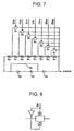
- the booster clock frequency is controlled by adjusting a booster clock generator circuit shown in Fig. 7.
- the frequency may be controlled by changing the division ratio of a frequency divider circuit although this would require a high oscillating frequency.
- a booster clock generator circuit includes inverters 51 and 52 which are connected in series.
- the output of the inverter 52 is positively fed back to the input of the inverter 51 via a capacitor 54.
- the output of the inverter 52 is negatively fed back to the input of the inverter 51 via an inverter 53 and resistors R 1 to R 8 connected in series to one another.
- the thus constructed components form a CR oscillator.
- Switching circuits S 1 to S 7 are connected so that one or more of the resistors R 1 to R 8 may be short-circuited, and the oscillating frequency of the CR oscillator may be changed based on the conditions of these switching circuits.
- Fig. 8 shows a specific example of a switching circuit.
- the switching circuit S 4 causes the resistors R 1 to R 4 to be shorted, with the oscillating frequency being set at the standard value.
- a control signal EN 3P supplied to the switching circuit S 7 is active, the resistors R 1 to R 7 are shorted, with the oscillating frequency being the maximum. If no control signal is active, on the other hand, none of the resistors is shorted, with the oscillating frequency being the minimum.
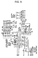
- the voltage V C between the two ends of the capacitor 6 shown in Fig. 2 is compared with three predetermined voltages V REF1 , V REF2 , and V REF3 in a time-division manner by a comparator 7 shown in Fig. 9.
- V REF1 V DD - V SS with V REF1 > V REF2 > (the desired margin voltage) > V REF3 .
- Serial/parallel conversion is performed on the output of the comparator 7 to yield individual flags A, B, and C as comparison results.
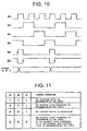
- switching circuits S11, S12, and S13 are incorporated. Also incorporated are flip-flops 61 to 64, which convert the output of the comparator 7 from serial to parallel. To these switching circuits and flip-flops, control clock signals ⁇ 2 to ⁇ 6 as depicted in Fig. 10 are supplied.
- the flags A and B are applied to non-inverting inputs of a NOR gate 65, and the flag C is applied to an inverting input of the NOR gate 65.
- the output of the NOR gate 65 is then forwarded to an inverting ENABLE input of an up-down counter 66 having a LOAD input as well as the ENABLE input.
- the up-down counter 66 is operated in accordance with a clock signal / ⁇ 6 .
- inverters 67 to 70 In association with each of the outputs of the up-down counter 66, there are provided respective inverters 67 to 70.
- the non-inverted and inverted outputs of the up-down counter 66 are fed to AND gates 71, 72, etc., so that one of the booster clock frequency control signals, EN 3M , EN 2M , etc., to be supplied to a booster clock generator circuit such as the one shown in Fig. 7, is asserted.
- the flag A and the control clock signal ⁇ 6 are supplied to an AND gate 73 as inputs thereto, and the flag C and the CARRY output of the up-down counter 66 are fed to inverting inputs of an AND gate 74.
- the outputs of the AND gates 73 and 74 are input to a NOR gate 75.
- the output of the NOR gate 75 is then fed to a CLOCK input of an up-down counter 76 having a LOAD input.
- inverters 77 and 78 In association with each of the outputs of the up-down counter 76, there are provided respective inverters 77 and 78.
- the non-inverted and inverted outputs of the up-down counter 76 are fed to AND gates 79 to 81, so that one of the boosting ratio control signals X1 to X3, which gates booster clock signals to be supplied to a booster circuit such as the one shown in Fig. 14, is asserted.
- Fig. 11 shows the specific control operations. If all the flags A, B, and C are 1 (at high level), the boosting ratio is decremented by one level. If the flag A is 0 and the flags B and C are 1, the booster clock frequency is decremented by one level. If the flags A and B are 0 and the flag C is 1, the current status is maintained. If all the flags A, B, and C are 0, the booster clock frequency is incremented by one level. If the booster clock frequency is already at the maximum level, however, the boosting ratio is instead incremented by one level.
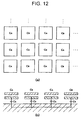
- stray capacitances C S are present between the semiconductor substrate and the lower electrodes of capacitors fabricated thereon.
- capacitors in this embodiment equivalently reduces such stray capacitances.
- the capacitors are fabricated in fragments on a semiconductor substrate.
- the fragmented capacitors are arranged in a checkered pattern and constitute of a first capacitor group C A and a second capacitor group C B .
- the numbers of capacitors included in the first and second capacitor groups C A and C B are, respectively, M and N, both being natural numbers.
- the capacitor groups C A and C B operate in the opposite phase from each other.
- the present invention even when the display mode or display content is changed, a margin for the boosted voltage is detected.
- power consumption can be reduced by either adjusting the frequency of clock signals or fixing at least one of the clock signals, which controls a switching component.
Landscapes
- Engineering & Computer Science (AREA)
- Power Engineering (AREA)
- Chemical & Material Sciences (AREA)
- Crystallography & Structural Chemistry (AREA)
- Physics & Mathematics (AREA)
- Computer Hardware Design (AREA)
- General Physics & Mathematics (AREA)
- Theoretical Computer Science (AREA)
- Dc-Dc Converters (AREA)
- Control Of Indicators Other Than Cathode Ray Tubes (AREA)
- Liquid Crystal Display Device Control (AREA)
Applications Claiming Priority (2)
| Application Number | Priority Date | Filing Date | Title |
|---|---|---|---|
| JP2000016171A JP3656495B2 (ja) | 2000-01-25 | 2000-01-25 | Dc−dc昇圧方法及びそれを用いた電源回路 |
| JP2000016171 | 2000-01-25 |
Publications (2)
| Publication Number | Publication Date |
|---|---|
| EP1126584A2 true EP1126584A2 (fr) | 2001-08-22 |
| EP1126584A3 EP1126584A3 (fr) | 2003-03-05 |
Family
ID=18543359
Family Applications (1)
| Application Number | Title | Priority Date | Filing Date |
|---|---|---|---|
| EP01101607A Withdrawn EP1126584A3 (fr) | 2000-01-25 | 2001-01-25 | Procédé d'élévation de tension courant continu - courant continu et circuit d'alimentation de puissance utilisant le même |
Country Status (4)
| Country | Link |
|---|---|
| US (1) | US6459330B2 (fr) |
| EP (1) | EP1126584A3 (fr) |
| JP (1) | JP3656495B2 (fr) |
| KR (1) | KR100402872B1 (fr) |
Cited By (1)
| Publication number | Priority date | Publication date | Assignee | Title |
|---|---|---|---|---|
| EP2264878A1 (fr) * | 2009-06-18 | 2010-12-22 | Intégration Dolphin Inc. | Convertisseur CC-CC doté d'une boucle de contrôle |
Families Citing this family (20)
| Publication number | Priority date | Publication date | Assignee | Title |
|---|---|---|---|---|
| JP4746205B2 (ja) * | 2001-06-12 | 2011-08-10 | Okiセミコンダクタ株式会社 | 昇圧回路及びこれを内蔵する半導体装置 |
| JP2003005724A (ja) * | 2001-06-25 | 2003-01-08 | Oki Micro Design Co Ltd | 液晶表示パネルの駆動電源回路 |
| TW578122B (en) * | 2002-06-05 | 2004-03-01 | Au Optronics Corp | Driving circuit for thin film transistor liquid crystal display |
| JP3741100B2 (ja) | 2002-11-26 | 2006-02-01 | セイコーエプソン株式会社 | 電源回路及び半導体集積回路 |
| JP3675455B2 (ja) | 2003-06-19 | 2005-07-27 | セイコーエプソン株式会社 | 昇圧回路、半導体装置及び表示装置 |
| JP3675456B2 (ja) | 2003-06-19 | 2005-07-27 | セイコーエプソン株式会社 | 半導体装置及び表示装置 |
| JP3675457B2 (ja) * | 2003-06-19 | 2005-07-27 | セイコーエプソン株式会社 | 昇圧クロック生成回路及び半導体装置 |
| JP3675454B2 (ja) | 2003-06-19 | 2005-07-27 | セイコーエプソン株式会社 | 昇圧回路、半導体装置及び表示装置 |
| JP4785410B2 (ja) * | 2004-06-01 | 2011-10-05 | セイコーインスツル株式会社 | 昇圧回路を有する電子機器 |
| JP4763371B2 (ja) * | 2005-07-25 | 2011-08-31 | 株式会社 日立ディスプレイズ | 表示装置 |
| CN100359551C (zh) * | 2005-11-02 | 2008-01-02 | 友达光电股份有限公司 | 显示装置及电源装置 |
| KR100761842B1 (ko) * | 2006-04-07 | 2007-09-28 | 삼성전자주식회사 | 가변되는 주파수를 가지는 승압 클럭신호를 이용하여 승압 동작을 수행하는 승압 회로 및 승압 방법 |
| JP4968904B2 (ja) * | 2006-12-08 | 2012-07-04 | ルネサスエレクトロニクス株式会社 | 表示パネル駆動装置、表示パネル駆動方法および表示装置 |
| KR20080111233A (ko) * | 2007-06-18 | 2008-12-23 | 삼성전자주식회사 | 액정 표시 장치의 구동 장치와 이를 포함하는 액정 표시장치 |
| JP4306768B2 (ja) * | 2007-06-18 | 2009-08-05 | エプソンイメージングデバイス株式会社 | 電気光学装置及び電子機器 |
| US7893745B2 (en) * | 2009-06-29 | 2011-02-22 | King Fahd University Of Petroleum And Minerals | Wideband programmable phase shifting circuit |
| US8461810B2 (en) | 2009-12-17 | 2013-06-11 | Magnachip Semiconductor, Ltd. | Circuit for generating boosted voltage and method for operating the same |
| KR101128690B1 (ko) * | 2009-12-17 | 2012-03-23 | 매그나칩 반도체 유한회사 | 승압전압 생성회로 및 이의 동작방법 |
| US20110199039A1 (en) * | 2010-02-17 | 2011-08-18 | Lansberry Geoffrey B | Fractional boost system |
| US20120133634A1 (en) * | 2010-11-30 | 2012-05-31 | Integrated Device Technology, Inc. | Apparatus, system, and method for generating a low power signal with an operational amplifier |
Citations (15)
| Publication number | Priority date | Publication date | Assignee | Title |
|---|---|---|---|---|
| GB2035629A (en) * | 1978-07-21 | 1980-06-18 | Rca Corp | Regulated high voltage power supply |
| JPS6439263A (en) * | 1987-08-03 | 1989-02-09 | Sharp Kk | Output voltage stabilization in booster circuit |
| EP0350462A2 (fr) * | 1988-07-06 | 1990-01-10 | STMicroelectronics S.r.l. | Régulation de la tension de sortie d'un multiplicateur de tension |
| JPH02179264A (ja) * | 1988-12-28 | 1990-07-12 | Nec Corp | 昇圧回路 |
| US5180991A (en) * | 1990-08-14 | 1993-01-19 | Oki Electric Industry Co., Ltd. | Frequency adjustable RC oscillator |
| US5414614A (en) * | 1994-06-06 | 1995-05-09 | Motorola, Inc. | Dynamically configurable switched capacitor power supply and method |
| FR2724468A1 (fr) * | 1994-09-14 | 1996-03-15 | Suisse Electronique Microtech | Dispositif electronique comportant un multiplicateur de tension |
| US5550728A (en) * | 1994-04-18 | 1996-08-27 | Analog Devices, Inc. | Charge pump converter structure |
| US5574634A (en) * | 1991-10-30 | 1996-11-12 | Xilinx, Inc. | Regulator for pumped voltage generator |
| EP0808014A2 (fr) * | 1996-05-17 | 1997-11-19 | Nec Corporation | Circuit élévateur de tension |
| EP0818875A2 (fr) * | 1996-07-08 | 1998-01-14 | Fujitsu Limited | Régulateur abaisseur de tension courant continu - courant continu |
| WO1998027477A1 (fr) * | 1996-12-18 | 1998-06-25 | Macronix International Co., Ltd. | Systeme de regulation pour pompes a charge |
| US5889441A (en) * | 1997-12-12 | 1999-03-30 | Scenix Semiconductor, Inc. | Temperature and voltage independent on-chip oscillator system and method |
| US5959853A (en) * | 1998-08-24 | 1999-09-28 | Kos; Marek John | Closed-loop switched capacitor network power supply |
| US6107950A (en) * | 1998-09-08 | 2000-08-22 | Intersil Corporation | Analog-to-digital converter having enhanced accuracy gain stage, and associated devices and methods |
Family Cites Families (10)
| Publication number | Priority date | Publication date | Assignee | Title |
|---|---|---|---|---|
| JPH03156511A (ja) | 1989-11-14 | 1991-07-04 | Seiko Epson Corp | 半導体装置 |
| WO1992003298A1 (fr) * | 1990-08-23 | 1992-03-05 | Seiko Epson Corporation | Carte memoire et appareil electronique l'utilisant |
| JP2614938B2 (ja) | 1990-10-25 | 1997-05-28 | 日本電気アイシーマイコンシステム株式会社 | チャージポンプ装置 |
| JPH0564429A (ja) | 1991-09-04 | 1993-03-12 | Seiko Epson Corp | 半導体装置及び電子機器 |
| JP3159586B2 (ja) | 1993-12-09 | 2001-04-23 | 株式会社東芝 | 昇圧回路装置 |
| KR0182039B1 (ko) * | 1995-12-13 | 1999-05-01 | 김광호 | 전원절감기능을 갖는 액정표시장치 |
| JPH09325318A (ja) * | 1996-06-04 | 1997-12-16 | Hitachi Ltd | 液晶表示装置 |
| JP3693464B2 (ja) | 1997-05-22 | 2005-09-07 | ローム株式会社 | 表示パネルの駆動装置 |
| JP3653165B2 (ja) * | 1997-07-09 | 2005-05-25 | アルプス電気株式会社 | 液晶表示装置の駆動電圧発生装置 |
| KR20000003732A (ko) * | 1998-06-29 | 2000-01-25 | 윤종용 | 전류 소비 절감 기능을 갖는 액정 구동 전압 발생 장치 |
-
2000
- 2000-01-25 JP JP2000016171A patent/JP3656495B2/ja not_active Expired - Lifetime
-
2001
- 2001-01-22 KR KR10-2001-0003553A patent/KR100402872B1/ko active IP Right Grant
- 2001-01-23 US US09/768,776 patent/US6459330B2/en not_active Expired - Lifetime
- 2001-01-25 EP EP01101607A patent/EP1126584A3/fr not_active Withdrawn
Patent Citations (15)
| Publication number | Priority date | Publication date | Assignee | Title |
|---|---|---|---|---|
| GB2035629A (en) * | 1978-07-21 | 1980-06-18 | Rca Corp | Regulated high voltage power supply |
| JPS6439263A (en) * | 1987-08-03 | 1989-02-09 | Sharp Kk | Output voltage stabilization in booster circuit |
| EP0350462A2 (fr) * | 1988-07-06 | 1990-01-10 | STMicroelectronics S.r.l. | Régulation de la tension de sortie d'un multiplicateur de tension |
| JPH02179264A (ja) * | 1988-12-28 | 1990-07-12 | Nec Corp | 昇圧回路 |
| US5180991A (en) * | 1990-08-14 | 1993-01-19 | Oki Electric Industry Co., Ltd. | Frequency adjustable RC oscillator |
| US5574634A (en) * | 1991-10-30 | 1996-11-12 | Xilinx, Inc. | Regulator for pumped voltage generator |
| US5550728A (en) * | 1994-04-18 | 1996-08-27 | Analog Devices, Inc. | Charge pump converter structure |
| US5414614A (en) * | 1994-06-06 | 1995-05-09 | Motorola, Inc. | Dynamically configurable switched capacitor power supply and method |
| FR2724468A1 (fr) * | 1994-09-14 | 1996-03-15 | Suisse Electronique Microtech | Dispositif electronique comportant un multiplicateur de tension |
| EP0808014A2 (fr) * | 1996-05-17 | 1997-11-19 | Nec Corporation | Circuit élévateur de tension |
| EP0818875A2 (fr) * | 1996-07-08 | 1998-01-14 | Fujitsu Limited | Régulateur abaisseur de tension courant continu - courant continu |
| WO1998027477A1 (fr) * | 1996-12-18 | 1998-06-25 | Macronix International Co., Ltd. | Systeme de regulation pour pompes a charge |
| US5889441A (en) * | 1997-12-12 | 1999-03-30 | Scenix Semiconductor, Inc. | Temperature and voltage independent on-chip oscillator system and method |
| US5959853A (en) * | 1998-08-24 | 1999-09-28 | Kos; Marek John | Closed-loop switched capacitor network power supply |
| US6107950A (en) * | 1998-09-08 | 2000-08-22 | Intersil Corporation | Analog-to-digital converter having enhanced accuracy gain stage, and associated devices and methods |
Non-Patent Citations (2)
| Title |
|---|
| PATENT ABSTRACTS OF JAPAN vol. 013, no. 232 (E-765), 29 May 1989 (1989-05-29) & JP 01 039263 A (SHARP CORPORATION), 9 February 1989 (1989-02-09) * |
| PATENT ABSTRACTS OF JAPAN vol. 014, no. 451 (E-984), 27 September 1990 (1990-09-27) & JP 02 179264 A (NEC CORP.), 12 July 1990 (1990-07-12) * |
Cited By (1)
| Publication number | Priority date | Publication date | Assignee | Title |
|---|---|---|---|---|
| EP2264878A1 (fr) * | 2009-06-18 | 2010-12-22 | Intégration Dolphin Inc. | Convertisseur CC-CC doté d'une boucle de contrôle |
Also Published As
| Publication number | Publication date |
|---|---|
| KR100402872B1 (ko) | 2003-10-22 |
| EP1126584A3 (fr) | 2003-03-05 |
| US20010024139A1 (en) | 2001-09-27 |
| JP3656495B2 (ja) | 2005-06-08 |
| JP2001211635A (ja) | 2001-08-03 |
| US6459330B2 (en) | 2002-10-01 |
| KR20010100772A (ko) | 2001-11-14 |
Similar Documents
| Publication | Publication Date | Title |
|---|---|---|
| US6459330B2 (en) | DC-DC voltage boosting method and power supply circuit using the same | |
| US6633287B1 (en) | Power supply circuit of an electro-optical device, driving circuit of an electro-optical device, method of driving an electro-optical device, electro-optical device, and electronic equipment | |
| US5635776A (en) | Charge pump voltage converter | |
| CN100390853C (zh) | 高效液晶显示器驱动电压发生电路及其方法 | |
| US7061481B2 (en) | Power supply circuit, operational amplifier circuit, liquid crystal device and electronic instrument | |
| EP1376529B1 (fr) | Dispositif d'affichage d'image et appareil électrique portable | |
| US6344984B1 (en) | Voltage multiplier having an intermediate tap | |
| JP3675454B2 (ja) | 昇圧回路、半導体装置及び表示装置 | |
| US7099167B2 (en) | Step-down circuit, power supply circuit, and semiconductor integrated circuit | |
| US5455534A (en) | Semiconductor device for liquid crystal panel driving power supply | |
| JPH10319368A (ja) | 表示パネルの駆動装置 | |
| US7148740B2 (en) | Boost circuit and semiconductor integrated circuit | |
| KR20000005986A (ko) | 액정표시패널구동용전원및그전력소비를감소시키기위한방법 | |
| US7138971B2 (en) | Power supply circuit for driving liquid crystal display | |
| KR20050008541A (ko) | 전원장치 | |
| JPWO2002039179A1 (ja) | 液晶表示装置 | |
| US7554537B2 (en) | Booster circuit, semiconductor device, and display device | |
| US7088356B2 (en) | Power source circuit | |
| JP3846478B2 (ja) | 昇圧回路、電源回路及び液晶駆動装置 | |
| US7538763B2 (en) | Semiconductor device and display device | |
| JP3180898B2 (ja) | 昇圧回路 | |
| JP2004343893A (ja) | 昇圧回路 | |
| US20070152931A1 (en) | LCD Driver | |
| US6798151B1 (en) | Current and charge leakage balancing device for display panel | |
| JP3139879B2 (ja) | 電源電圧変換回路 |
Legal Events
| Date | Code | Title | Description |
|---|---|---|---|
| PUAI | Public reference made under article 153(3) epc to a published international application that has entered the european phase |
Free format text: ORIGINAL CODE: 0009012 |
|
| AK | Designated contracting states |
Kind code of ref document: A2 Designated state(s): AT BE CH CY DE DK ES FI FR GB GR IE IT LI LU MC NL PT SE TR |
|
| AX | Request for extension of the european patent |
Free format text: AL;LT;LV;MK;RO;SI |
|
| PUAL | Search report despatched |
Free format text: ORIGINAL CODE: 0009013 |
|
| AK | Designated contracting states |
Kind code of ref document: A3 Designated state(s): AT BE CH CY DE DK ES FI FR GB GR IE IT LI LU MC NL PT SE TR Designated state(s): AT BE CH CY DE DK ES FI FR GB GR IE IT LI LU MC NL PT SE TR |
|
| AX | Request for extension of the european patent |
Extension state: AL LT LV MK RO SI |
|
| 17P | Request for examination filed |
Effective date: 20030825 |
|
| AKX | Designation fees paid |
Designated state(s): AT BE CH CY DE DK ES FI FR GB GR IE IT LI LU MC NL PT SE TR |
|
| 17Q | First examination report despatched |
Effective date: 20090422 |
|
| STAA | Information on the status of an ep patent application or granted ep patent |
Free format text: STATUS: THE APPLICATION HAS BEEN WITHDRAWN |
|
| 18W | Application withdrawn |
Effective date: 20090930 |