EP0350462A2 - Régulation de la tension de sortie d'un multiplicateur de tension - Google Patents
Régulation de la tension de sortie d'un multiplicateur de tension Download PDFInfo
- Publication number
- EP0350462A2 EP0350462A2 EP89830291A EP89830291A EP0350462A2 EP 0350462 A2 EP0350462 A2 EP 0350462A2 EP 89830291 A EP89830291 A EP 89830291A EP 89830291 A EP89830291 A EP 89830291A EP 0350462 A2 EP0350462 A2 EP 0350462A2
- Authority
- EP
- European Patent Office
- Prior art keywords
- voltage
- current
- signal
- transistor
- inverter
- Prior art date
- Legal status (The legal status is an assumption and is not a legal conclusion. Google has not performed a legal analysis and makes no representation as to the accuracy of the status listed.)
- Granted
Links
- 230000001105 regulatory effect Effects 0.000 claims abstract description 20
- 230000010355 oscillation Effects 0.000 claims abstract description 15
- 239000003990 capacitor Substances 0.000 claims description 8
- 230000000630 rising effect Effects 0.000 claims 1
- 230000001276 controlling effect Effects 0.000 abstract description 2
- QHGVXILFMXYDRS-UHFFFAOYSA-N pyraclofos Chemical compound C1=C(OP(=O)(OCC)SCCC)C=NN1C1=CC=C(Cl)C=C1 QHGVXILFMXYDRS-UHFFFAOYSA-N 0.000 description 4
- 238000010586 diagram Methods 0.000 description 3
- SILSDTWXNBZOGF-KUZBFYBWSA-N chembl111058 Chemical compound CCSC(C)CC1CC(O)=C(\C(CC)=N\OC\C=C\Cl)C(=O)C1 SILSDTWXNBZOGF-KUZBFYBWSA-N 0.000 description 2
- 238000000034 method Methods 0.000 description 2
- 239000002699 waste material Substances 0.000 description 2
- 238000010521 absorption reaction Methods 0.000 description 1
- 210000004899 c-terminal region Anatomy 0.000 description 1
- 230000003071 parasitic effect Effects 0.000 description 1
- 230000010363 phase shift Effects 0.000 description 1
- 238000005086 pumping Methods 0.000 description 1
- 230000000087 stabilizing effect Effects 0.000 description 1
- 230000003245 working effect Effects 0.000 description 1
Images

Classifications
-
- G—PHYSICS
- G11—INFORMATION STORAGE
- G11C—STATIC STORES
- G11C5/00—Details of stores covered by group G11C11/00
- G11C5/14—Power supply arrangements, e.g. power down, chip selection or deselection, layout of wirings or power grids, or multiple supply levels
- G11C5/145—Applications of charge pumps; Boosted voltage circuits; Clamp circuits therefor
-
- G—PHYSICS
- G11—INFORMATION STORAGE
- G11C—STATIC STORES
- G11C16/00—Erasable programmable read-only memories
- G11C16/02—Erasable programmable read-only memories electrically programmable
- G11C16/06—Auxiliary circuits, e.g. for writing into memory
- G11C16/30—Power supply circuits
-
- H—ELECTRICITY
- H02—GENERATION; CONVERSION OR DISTRIBUTION OF ELECTRIC POWER
- H02M—APPARATUS FOR CONVERSION BETWEEN AC AND AC, BETWEEN AC AND DC, OR BETWEEN DC AND DC, AND FOR USE WITH MAINS OR SIMILAR POWER SUPPLY SYSTEMS; CONVERSION OF DC OR AC INPUT POWER INTO SURGE OUTPUT POWER; CONTROL OR REGULATION THEREOF
- H02M3/00—Conversion of dc power input into dc power output
- H02M3/02—Conversion of dc power input into dc power output without intermediate conversion into ac
- H02M3/04—Conversion of dc power input into dc power output without intermediate conversion into ac by static converters
- H02M3/06—Conversion of dc power input into dc power output without intermediate conversion into ac by static converters using resistors or capacitors, e.g. potential divider
- H02M3/07—Conversion of dc power input into dc power output without intermediate conversion into ac by static converters using resistors or capacitors, e.g. potential divider using capacitors charged and discharged alternately by semiconductor devices with control electrode, e.g. charge pumps
- H02M3/073—Charge pumps of the Schenkel-type
Definitions
- the present invention relates to a circuit for regulating the output voltage of a voltage multiplier which is particularly effective in reducing power consumption.
- This circuit is well known and described in literature and is commonly as severelysociated with an oscillator which produces two signals with a 180° phase-shift between them, necessary for driving electric charge transfer through the various stages of the voltage multiplier, each stage being formed essentially by a diode and by a capacitor, in a single direction from a supply terminal to an output capacitor across which the multiplied voltage is produced, and with control means of the output voltage for keeping it constant independently from the load and/or from changes of the supply voltage.
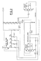
- FIG. 1 A complete voltage multiplier system which is commonly used in integrated circuits is depicted in Fig. 1.
- the voltage multiplier is a four stage circuit, each stage being formed by a diode (diode connect ed transistor) and by a capacitor, connected so as to transfer the charge in a single direction from an input terminal to an output terminal thereof, i.e. from the supply terminal VCC to the output capacitor COUT.
- the oscillator generating the two driving signals phi 1 and phi 2, with a 180° phase difference for driving the voltage multiplier is a common ring-type oscillator, wherein one of the three inverters composing it is substituted by a Schmitt trigger in order to achieve a greater ring's gain, and a second inverter is substituted by a NOR gate in order to permit interruption of the oscillation by applying a logic stop signal to the C terminal.
- the regulation means of the output voltage of the voltage multiplier is, as customary, formed by a "chain" of series-connected diodes (diode-connected transistors) connected between the high voltage (HV) output terminal and ground; the output voltage being adjusted to a value corresponding to the sum of the threshold voltages of the diode-connected transistors forming the chain.
- the regulation means may also be implemented by means of one or more Zener diodes or by one or more parasitic transistors, according to techniques which are well known to the skilled technician.
- the operating frequency of the oscillator must be set at least to a value sufficient to generate such a contemplated maximum current to be delivered.
- the frequency will be sensibly higher when the supply voltage is 5.5 V with a consequent sensible increase of the current delivered by the voltage multiplier and therefore of the power consumption in general.
- the present invention has as an objective an improved circuit for regulating the output voltage of a voltage multiplier capable of effectively limiting the power consumption.
- the solution provided contemplates controlling the frequency of oscillation of the oscillator which generates the two driving signals phi 1 and phi 2 of the voltage multiplier circuit in function of the current delivered by the latter.
- the improved circuit of the invention for regulating the output voltage of a voltage multipling system for a supply voltage VCC is depicted in Fig. 2.
- the circuit blocks relative to the voltage multiplier circuit and to the ring oscillator driving it may be, as shown in Fig. 2, similar to those utilized in the prior art system as schematically depicted in Fig. 1.
- the regulating means of the HV output voltage of the voltage multiplier which, in the example shown, may be a chain of diode-connected transistors (p-channel transistors in the case depicted) presenting a total threshold voltage substantially equal to the regulated voltage desired, has a transistor T1, functioning as a current generator, whereby the Vgs (gate-source voltage) thereof is kept substantially constant independently of the supply voltage, connected in series thereto.
- the gate of the transistor T1 is biased at a constant voltage Vref, which may be obtained by means of a conventional reference constant voltage generator (not shown in Fig. 2), thus setting a certain reference current Iref through the transistor T1, which current may conveniently be about 1 microamperes.
- the HV output voltage of the circuit will be initially equal to the supply voltage VCC less the voltage drop across the five diode-connected transistors of the five stages of the voltage multiplier circuit respectively. If the chain of diode-connected transistors which regulates the output voltage has for example, a total threshold voltage of 12 V, until the output voltage HV reaches such a value no current will flow through the regulation chain and therefore the voltage HV - REG across the transistor T1 will be substantially at ground potential because of the relatively small current: Iref, imposed by the current generator formed by the transistor T1.
- the HV - REG signal is on the other hand fed to the input of an inverter 1 and the corresponding output signal of the inverter 1 is fed to the input of a Schmitt trigger the output signal of which is fed to the enable terminal C of the ring oscillator (i.e. of the NOR gate which substitutes one of the inverters which functionally form a ring oscillator).
- the output HV voltage of the voltage multiplier will reach the threshold voltage determined by the regulating chain of diode-connected transistors, and through the chain the current which is not absorbed by the circuits fed with the high voltage HV will be discharged to ground. As soon as the value of such a current discharged to ground becomes higher than the current imposed by the current generator T1, i.e.
- the potential of the node HV - REG will start to rise and eventually, through the suitably unbalanced inverter 1 and the Schmitt trigger which regenerates the phase of the signal and amplifies it to a full logic value, the STOPOSC signal will stop the oscillator.
- the voltage multiplier circuit may no longer transfer electric charge to the output capacitor COUT, which begins to discharge and the output voltage HV slowly drops until the regulating chain is no longer capable of letting discharge current through because the voltage across the chain has fallen below the total threshold voltage thereof.
- the starting situation wherein the HV - REG signal assumes a ground potential and the oscillator is again free to oscillate is therefore re-established. In this situation, just few oscillations may be sufficient to rise the output voltage HV again to the value at which the regulating circuit intervenes again to stop the oscillator and so on, until, in the limit, even a single oscillation will suffice.
- Schmitt trigger within the ring oscillator frequency regulation network, as shown in the embodiment of Fig. 2, is not strictly necessary, being the Schmitt trigger easily replaceable by any amplifying stage capable of producing through an output terminal thereof a signal of a desired level in function of the output signal of the first inverter 1 and regenerated in term of phase in respect of said HV - REG signal.
- diode often used in the specification and in the claims for describing the elements composing said regulating chain, it is intended to indicate any structure functionally equivalent to a diode.
Applications Claiming Priority (2)
| Application Number | Priority Date | Filing Date | Title |
|---|---|---|---|
| IT8883647A IT1225608B (it) | 1988-07-06 | 1988-07-06 | Regolazione della tensione prodotta da un moltiplicatore di tensione. |
| IT8364788 | 1988-07-06 |
Publications (3)
| Publication Number | Publication Date |
|---|---|
| EP0350462A2 true EP0350462A2 (fr) | 1990-01-10 |
| EP0350462A3 EP0350462A3 (en) | 1990-05-30 |
| EP0350462B1 EP0350462B1 (fr) | 1993-11-10 |
Family
ID=11323612
Family Applications (1)
| Application Number | Title | Priority Date | Filing Date |
|---|---|---|---|
| EP89830291A Expired - Lifetime EP0350462B1 (fr) | 1988-07-06 | 1989-06-23 | Régulation de la tension de sortie d'un multiplicateur de tension |
Country Status (5)
| Country | Link |
|---|---|
| US (2) | US4933827A (fr) |
| EP (1) | EP0350462B1 (fr) |
| JP (1) | JPH0265269A (fr) |
| DE (1) | DE68910597T2 (fr) |
| IT (1) | IT1225608B (fr) |
Cited By (24)
| Publication number | Priority date | Publication date | Assignee | Title |
|---|---|---|---|---|
| GB2237667A (en) * | 1989-10-31 | 1991-05-08 | Mitsubishi Electric Corp | Portable memory card with onboard voltage generator |
| FR2667169A1 (fr) * | 1990-09-25 | 1992-03-27 | Samsung Electronics Co Ltd | Circuit de production de haute tension pour un circuit de memoire a semiconducteur. |
| EP0498251A2 (fr) * | 1991-02-05 | 1992-08-12 | International Business Machines Corporation | Circuit d'attaque de ligne de mot pour mémoires dynamiques à accès aléatoire |
| WO1993014555A1 (fr) * | 1992-01-14 | 1993-07-22 | Sierra Semiconductor B.V. | Circuit de reaction pour generateur de haute tension de cmos servant a programmer des cellules de memoire (e)eprom |
| EP0591022A1 (fr) * | 1992-10-01 | 1994-04-06 | STMicroelectronics S.A. | Circuit élévateur de tension de type pompe de charge avec oscillateur bootstrappe |
| WO1995000953A1 (fr) * | 1993-06-28 | 1995-01-05 | National Semiconductor Corporation | Generateur de haute tension constante |
| EP0644646A1 (fr) * | 1993-09-22 | 1995-03-22 | Advanced Micro Devices, Inc. | Circuit élévateur de tension pour faible puissance |
| EP0655827A1 (fr) * | 1993-11-30 | 1995-05-31 | Nec Corporation | Circuit générateur de tension constante avec circuit élévateur de tension |
| FR2724468A1 (fr) * | 1994-09-14 | 1996-03-15 | Suisse Electronique Microtech | Dispositif electronique comportant un multiplicateur de tension |
| EP0658904A3 (fr) * | 1993-12-17 | 1996-06-05 | Hitachi Ltd | Dispositif de circuit intégré à semi-conducteur. |
| EP0758499A1 (fr) * | 1994-03-23 | 1997-02-19 | Intel Corporation | Procede et appareil permettant d'obtenir une pompe a charge negative a puissance ultra-faible |
| EP0782149A2 (fr) * | 1995-12-29 | 1997-07-02 | STMicroelectronics S.r.l. | Dispositif pour la génération et régulation d'une tension de grille dans une mémoire non-volatile |
| WO1997037424A1 (fr) * | 1996-03-28 | 1997-10-09 | Siemens Aktiengesellschaft | Montage d'alimentation pour un circuit de charge electronique |
| EP0805456A1 (fr) * | 1996-04-30 | 1997-11-05 | STMicroelectronics S.r.l. | Circuit de polarisation pour des cellules VPROM à basse tension |
| WO1998001938A1 (fr) * | 1996-07-05 | 1998-01-15 | Siemens Aktiengesellschaft | Dispositif permettant de multiplier une tension sans faire dependre la tension de sortie de la tension d'alimentation |
| WO1998013927A1 (fr) * | 1996-09-26 | 1998-04-02 | Siemens Aktiengesellschaft | Circuit de regulation pour pompes de charge |
| EP0866545A1 (fr) * | 1997-03-19 | 1998-09-23 | STMicroelectronics S.A. | Circuit élévateur de tension du type pompe de charge à nombre d'étages contrÔlé |
| FR2783617A1 (fr) * | 1998-09-18 | 2000-03-24 | St Microelectronics Sa | Systeme de regulation d'une pompe de charge |
| EP0755119B1 (fr) * | 1995-07-20 | 2000-05-17 | Mhs | Dispositif de mise en forme d'un signal analogique en un signal rectangulaire |
| EP1014547A2 (fr) * | 1998-12-21 | 2000-06-28 | Fairchild Semiconductor Corporation | Système de pompe de charge à courant bas |
| EP1126584A2 (fr) * | 2000-01-25 | 2001-08-22 | Seiko Epson Corporation | Procédé d'élévation de tension courant continu - courant continu et circuit d'alimentation de puissance utilisant le même |
| WO2003052567A2 (fr) * | 2001-12-18 | 2003-06-26 | Intel Corporation | Dispositif flash fonctionnant a partir d'une alimentation electrique en boitier ou d'une alimentation electrique sur puce |
| FR2878986A1 (fr) * | 2004-12-08 | 2006-06-09 | Atmel Corp | Principe de regulation de puissance d'une sortie a haute tension dans des dispositifs de circuits integres |
| CN102777383A (zh) * | 2011-05-05 | 2012-11-14 | 江森自控科技公司 | 压缩机 |
Families Citing this family (22)
| Publication number | Priority date | Publication date | Assignee | Title |
|---|---|---|---|---|
| JPH04372571A (ja) * | 1991-06-19 | 1992-12-25 | Nec Ic Microcomput Syst Ltd | 定電圧発生回路 |
| JPH05111242A (ja) * | 1991-09-17 | 1993-04-30 | Samsung Electron Co Ltd | 半導体装置の定電圧発生器 |
| US5216588A (en) * | 1992-02-14 | 1993-06-01 | Catalyst Semiconductor, Inc. | Charge pump with high output current |
| DE69226627T2 (de) * | 1992-05-15 | 1998-12-24 | Sgs Thomson Microelectronics | Generator für Signale mit höher Frequenz und nicht-überlappenden Phasen |
| US5301097A (en) * | 1992-06-10 | 1994-04-05 | Intel Corporation | Multi-staged charge-pump with staggered clock phases for providing high current capability |
| DE69312305T2 (de) * | 1993-12-28 | 1998-01-15 | Sgs Thomson Microelectronics | Spannungsbooster, insbesondere für nichtflüchtige Speicher |
| EP0691729A3 (fr) * | 1994-06-30 | 1996-08-14 | Sgs Thomson Microelectronics | Circuit pompe de charge à commande asservi |
| JP3184065B2 (ja) * | 1994-07-25 | 2001-07-09 | セイコーインスツルメンツ株式会社 | 半導体集積回路装置及び電子機器 |
| DE4443690A1 (de) * | 1994-12-08 | 1996-06-20 | Martin Prof Dr Poppe | Monolithische integrierbare Schaltung zur Gleichspannungswandlung |
| US5793246A (en) * | 1995-11-08 | 1998-08-11 | Altera Corporation | High voltage pump scheme incorporating an overlapping clock |
| US5883544A (en) * | 1996-12-03 | 1999-03-16 | Stmicroelectronics, Inc. | Integrated circuit actively biasing the threshold voltage of transistors and related methods |
| US5939934A (en) * | 1996-12-03 | 1999-08-17 | Stmicroelectronics, Inc. | Integrated circuit passively biasing transistor effective threshold voltage and related methods |
| US5834966A (en) * | 1996-12-08 | 1998-11-10 | Stmicroelectronics, Inc. | Integrated circuit sensing and digitally biasing the threshold voltage of transistors and related methods |
| US5929695A (en) * | 1997-06-02 | 1999-07-27 | Stmicroelectronics, Inc. | Integrated circuit having selective bias of transistors for low voltage and low standby current and related methods |
| US6430067B1 (en) * | 2001-04-12 | 2002-08-06 | Sun Microsystems, Inc. | Voltage multiplier for low voltage microprocessor |
| DE10297335T5 (de) * | 2002-09-11 | 2004-11-18 | Mitsubishi Denki K.K. | Spannungserfassungsschaltung und dieselbe benutzende Erzeugungsschaltung für interne Spannung |
| TWI220588B (en) * | 2003-05-15 | 2004-08-21 | Amic Technology Corp | Regulated charge pump |
| WO2005043733A1 (fr) * | 2003-11-03 | 2005-05-12 | Koninklijke Philips Electronics N.V. | Appareil fonctionnant comme pompe de charge a haute tension et circuit correspondant |
| US7372318B2 (en) * | 2004-07-26 | 2008-05-13 | Honeywell International Inc. | Precision, low drift, stacked voltage reference |
| US8736351B2 (en) * | 2011-01-13 | 2014-05-27 | Taiwan Semiconductor Manufacturing Co., Ltd. | Negative charge pump |
| EP2827483A1 (fr) * | 2013-07-15 | 2015-01-21 | Infineon Technologies AG | Circuit, pompe de charge à branches multiples, procédé de commande d'une pompe de charge et système |
| CN110463002B (zh) | 2017-02-16 | 2023-05-09 | 瑞声科技(新加坡)有限公司 | 电荷泵系统、设备和方法 |
Citations (2)
| Publication number | Priority date | Publication date | Assignee | Title |
|---|---|---|---|---|
| US4322675A (en) * | 1980-11-03 | 1982-03-30 | Fairchild Camera & Instrument Corp. | Regulated MOS substrate bias voltage generator for a static random access memory |
| EP0144637A2 (fr) * | 1983-11-14 | 1985-06-19 | International Business Machines Corporation | Système de génération de tension pour une mémoire R.A.M. non-volatile |
Family Cites Families (8)
| Publication number | Priority date | Publication date | Assignee | Title |
|---|---|---|---|---|
| US4250414A (en) * | 1978-07-31 | 1981-02-10 | Bell Telephone Laboratories, Incorporated | Voltage generator circuitry |
| US4302804A (en) * | 1979-09-04 | 1981-11-24 | Burroughs Corporation | DC Voltage multiplier using phase-sequenced CMOS switches |
| US4346310A (en) * | 1980-05-09 | 1982-08-24 | Motorola, Inc. | Voltage booster circuit |
| US4344003A (en) * | 1980-08-04 | 1982-08-10 | Rca Corporation | Low power voltage multiplier circuit |
| JPS57204640A (en) * | 1981-06-12 | 1982-12-15 | Fujitsu Ltd | Generating circuit of substrate bias voltage |
| JPS6159688A (ja) * | 1984-08-31 | 1986-03-27 | Hitachi Ltd | 半導体集積回路装置 |
| JPS61268053A (ja) * | 1985-05-22 | 1986-11-27 | Mitsubishi Electric Corp | 昇圧回路 |
| US4621315A (en) * | 1985-09-03 | 1986-11-04 | Motorola, Inc. | Recirculating MOS charge pump |
-
1988
- 1988-07-06 IT IT8883647A patent/IT1225608B/it active
-
1989
- 1989-06-23 EP EP89830291A patent/EP0350462B1/fr not_active Expired - Lifetime
- 1989-06-23 DE DE89830291T patent/DE68910597T2/de not_active Expired - Fee Related
- 1989-07-06 US US07/376,267 patent/US4933827A/en not_active Ceased
- 1989-07-06 JP JP1175409A patent/JPH0265269A/ja active Pending
-
1992
- 1992-06-09 US US07/897,443 patent/USRE35121E/en not_active Expired - Lifetime
Patent Citations (2)
| Publication number | Priority date | Publication date | Assignee | Title |
|---|---|---|---|---|
| US4322675A (en) * | 1980-11-03 | 1982-03-30 | Fairchild Camera & Instrument Corp. | Regulated MOS substrate bias voltage generator for a static random access memory |
| EP0144637A2 (fr) * | 1983-11-14 | 1985-06-19 | International Business Machines Corporation | Système de génération de tension pour une mémoire R.A.M. non-volatile |
Cited By (50)
| Publication number | Priority date | Publication date | Assignee | Title |
|---|---|---|---|---|
| GB2237667B (en) * | 1989-10-31 | 1994-05-11 | Mitsubishi Electric Corp | Portable semiconductor memory unit |
| US5172342A (en) * | 1989-10-31 | 1992-12-15 | Mitsubishi Denki Kabushiki Kaisha | Portable semiconductor memory unit |
| GB2237667A (en) * | 1989-10-31 | 1991-05-08 | Mitsubishi Electric Corp | Portable memory card with onboard voltage generator |
| FR2667169A1 (fr) * | 1990-09-25 | 1992-03-27 | Samsung Electronics Co Ltd | Circuit de production de haute tension pour un circuit de memoire a semiconducteur. |
| EP0498251A2 (fr) * | 1991-02-05 | 1992-08-12 | International Business Machines Corporation | Circuit d'attaque de ligne de mot pour mémoires dynamiques à accès aléatoire |
| EP0498251A3 (en) * | 1991-02-05 | 1993-11-24 | Ibm | Word line driver circuit for dynamic random access memories |
| WO1993014555A1 (fr) * | 1992-01-14 | 1993-07-22 | Sierra Semiconductor B.V. | Circuit de reaction pour generateur de haute tension de cmos servant a programmer des cellules de memoire (e)eprom |
| US5546031A (en) * | 1992-01-14 | 1996-08-13 | Sierra Semiconductor B.V. | Feed-back circuit for CMOS high voltage generator to program (E) eprom-memory cells |
| FR2696598A1 (fr) * | 1992-10-01 | 1994-04-08 | Sgs Thomson Microelectronics | Circuit élévateur de tension de type pompe de charge avec oscillateur bootstrapé. |
| EP0591022A1 (fr) * | 1992-10-01 | 1994-04-06 | STMicroelectronics S.A. | Circuit élévateur de tension de type pompe de charge avec oscillateur bootstrappe |
| US5589793A (en) * | 1992-10-01 | 1996-12-31 | Sgs-Thomson Microelectronics S.A. | Voltage booster circuit of the charge-pump type with bootstrapped oscillator |
| US5592115A (en) * | 1992-10-01 | 1997-01-07 | Sgs-Thomson Microelectronics S.A. | Voltage booster circuit of the charge-pump type with a bootstrapped oscillator |
| WO1995000953A1 (fr) * | 1993-06-28 | 1995-01-05 | National Semiconductor Corporation | Generateur de haute tension constante |
| EP0644646A1 (fr) * | 1993-09-22 | 1995-03-22 | Advanced Micro Devices, Inc. | Circuit élévateur de tension pour faible puissance |
| US5526253A (en) * | 1993-09-22 | 1996-06-11 | Advanced Micro Devices, Inc. | Low power voltage boost circuit with regulated output |
| EP0655827A1 (fr) * | 1993-11-30 | 1995-05-31 | Nec Corporation | Circuit générateur de tension constante avec circuit élévateur de tension |
| US5499183A (en) * | 1993-11-30 | 1996-03-12 | Nec Corporation | Constant voltage generating circuit having step-up circuit |
| EP0658904A3 (fr) * | 1993-12-17 | 1996-06-05 | Hitachi Ltd | Dispositif de circuit intégré à semi-conducteur. |
| EP0758499A1 (fr) * | 1994-03-23 | 1997-02-19 | Intel Corporation | Procede et appareil permettant d'obtenir une pompe a charge negative a puissance ultra-faible |
| EP0758499A4 (fr) * | 1994-03-23 | 1997-06-04 | Intel Corp | Procede et appareil permettant d'obtenir une pompe a charge negative a puissance ultra-faible |
| FR2724468A1 (fr) * | 1994-09-14 | 1996-03-15 | Suisse Electronique Microtech | Dispositif electronique comportant un multiplicateur de tension |
| EP0755119B1 (fr) * | 1995-07-20 | 2000-05-17 | Mhs | Dispositif de mise en forme d'un signal analogique en un signal rectangulaire |
| EP0782149A2 (fr) * | 1995-12-29 | 1997-07-02 | STMicroelectronics S.r.l. | Dispositif pour la génération et régulation d'une tension de grille dans une mémoire non-volatile |
| EP0782149A3 (fr) * | 1995-12-29 | 1998-08-19 | STMicroelectronics S.r.l. | Dispositif pour la génération et régulation d'une tension de grille dans une mémoire non-volatile |
| WO1997037424A1 (fr) * | 1996-03-28 | 1997-10-09 | Siemens Aktiengesellschaft | Montage d'alimentation pour un circuit de charge electronique |
| US6026002A (en) * | 1996-03-28 | 2000-02-15 | Siemens Aktiengesellschaft | Circuit configuration for supplying an electronic load circuit |
| US5859797A (en) * | 1996-04-30 | 1999-01-12 | Sgs-Thomson Microelectronics S.R.L. | Biasing circuit for UPROM cells with low voltage supply |
| EP0805456A1 (fr) * | 1996-04-30 | 1997-11-05 | STMicroelectronics S.r.l. | Circuit de polarisation pour des cellules VPROM à basse tension |
| WO1998001938A1 (fr) * | 1996-07-05 | 1998-01-15 | Siemens Aktiengesellschaft | Dispositif permettant de multiplier une tension sans faire dependre la tension de sortie de la tension d'alimentation |
| US6172886B1 (en) | 1996-07-05 | 2001-01-09 | Siemens Aktiengesellschaft | Apparatus for voltage multiplication with output voltage having low dependence on supply voltage |
| DE19627197C1 (de) * | 1996-07-05 | 1998-03-26 | Siemens Ag | Vorrichtung zur Spannungsvervielfachung mit geringer Abhängigkeit der Ausgangsspannung von der Versorgungsspannung |
| WO1998013927A1 (fr) * | 1996-09-26 | 1998-04-02 | Siemens Aktiengesellschaft | Circuit de regulation pour pompes de charge |
| EP0866545A1 (fr) * | 1997-03-19 | 1998-09-23 | STMicroelectronics S.A. | Circuit élévateur de tension du type pompe de charge à nombre d'étages contrÔlé |
| US5999040A (en) * | 1997-03-19 | 1999-12-07 | Stmicroelectronics S.A. | Voltage booster circuit with controlled number of stages |
| FR2761214A1 (fr) * | 1997-03-19 | 1998-09-25 | Sgs Thomson Microelectronics | Circuit elevateur de tension du type pompe de charge a nombre d'etages controle |
| FR2783617A1 (fr) * | 1998-09-18 | 2000-03-24 | St Microelectronics Sa | Systeme de regulation d'une pompe de charge |
| US6373328B2 (en) | 1998-12-21 | 2002-04-16 | Fairchild Semiconductor Corporation | Comparator circuit |
| EP1014547A3 (fr) * | 1998-12-21 | 2000-11-15 | Fairchild Semiconductor Corporation | Système de pompe de charge à courant bas |
| EP1014547A2 (fr) * | 1998-12-21 | 2000-06-28 | Fairchild Semiconductor Corporation | Système de pompe de charge à courant bas |
| US6452440B2 (en) | 1998-12-21 | 2002-09-17 | Fairchild Semiconductor Corporation | Voltage divider circuit |
| EP1126584A2 (fr) * | 2000-01-25 | 2001-08-22 | Seiko Epson Corporation | Procédé d'élévation de tension courant continu - courant continu et circuit d'alimentation de puissance utilisant le même |
| US6459330B2 (en) | 2000-01-25 | 2002-10-01 | Seiko Epson Corporation | DC-DC voltage boosting method and power supply circuit using the same |
| EP1126584A3 (fr) * | 2000-01-25 | 2003-03-05 | Seiko Epson Corporation | Procédé d'élévation de tension courant continu - courant continu et circuit d'alimentation de puissance utilisant le même |
| WO2003052567A2 (fr) * | 2001-12-18 | 2003-06-26 | Intel Corporation | Dispositif flash fonctionnant a partir d'une alimentation electrique en boitier ou d'une alimentation electrique sur puce |
| WO2003052567A3 (fr) * | 2001-12-18 | 2004-03-11 | Intel Corp | Dispositif flash fonctionnant a partir d'une alimentation electrique en boitier ou d'une alimentation electrique sur puce |
| KR100737038B1 (ko) * | 2001-12-18 | 2007-07-09 | 인텔 코포레이션 | 메모리 블록과 프로세서를 포함하는 시스템 및 방법, 및패키지 장치 |
| FR2878986A1 (fr) * | 2004-12-08 | 2006-06-09 | Atmel Corp | Principe de regulation de puissance d'une sortie a haute tension dans des dispositifs de circuits integres |
| US7808300B2 (en) | 2004-12-08 | 2010-10-05 | Atmel Corporation | Power regulation scheme for a high voltage output in integrated circuit devices |
| CN102777383A (zh) * | 2011-05-05 | 2012-11-14 | 江森自控科技公司 | 压缩机 |
| CN102777383B (zh) * | 2011-05-05 | 2015-05-20 | 江森自控科技公司 | 压缩机 |
Also Published As
| Publication number | Publication date |
|---|---|
| IT1225608B (it) | 1990-11-22 |
| JPH0265269A (ja) | 1990-03-05 |
| EP0350462B1 (fr) | 1993-11-10 |
| EP0350462A3 (en) | 1990-05-30 |
| IT8883647A0 (it) | 1988-07-06 |
| DE68910597T2 (de) | 1994-03-03 |
| USRE35121E (en) | 1995-12-12 |
| US4933827A (en) | 1990-06-12 |
| DE68910597D1 (de) | 1993-12-16 |
Similar Documents
| Publication | Publication Date | Title |
|---|---|---|
| EP0350462A2 (fr) | Régulation de la tension de sortie d'un multiplicateur de tension | |
| US5258662A (en) | Micropower gate charge pump for power MOSFETS | |
| USRE35041E (en) | Inductance and capacitance charge pump circuit for driving power MOS transistor bridges | |
| EP0477108B1 (fr) | Générateur de tension pour un circuit intégré à semi-conducteur | |
| US3733540A (en) | Switching regulator sweep starting protection circuit | |
| US5694308A (en) | Method and apparatus for regulated low voltage charge pump | |
| US5663877A (en) | Synchronous rectifier that is impervious to reverse feed | |
| US6275395B1 (en) | Accelerated turn-off of MOS transistors by bootstrapping | |
| US4656369A (en) | Ring oscillator substrate bias generator with precharge voltage feedback control | |
| US4374357A (en) | Switched capacitor precision current source | |
| JP2638533B2 (ja) | 不揮発性メモリ用電圧ブースタ | |
| EP0032588A2 (fr) | Circuit générateur de polarisation de substrat | |
| EP0691729A2 (fr) | Circuit pompe de charge à commande asservi | |
| GB2232829A (en) | An internal voltage converter in a semiconductor integrated circuit | |
| WO1990008426A1 (fr) | Appareil generateur et regulateur de tension de polarisation de substrat | |
| JP2004173481A (ja) | スイッチングレギュレータ及び電源装置 | |
| US9106149B2 (en) | Start-up circuitry | |
| US6300839B1 (en) | Frequency controlled system for positive voltage regulation | |
| JPH0793820B2 (ja) | 直流電圧発生回路 | |
| EP0395558A2 (fr) | Convertisseur de courant continu | |
| US20030218453A1 (en) | Voltage regulator for a charge pump circuit | |
| US11374579B2 (en) | Charge pump with load driven clock frequency management | |
| US6483376B1 (en) | Voltage generation circuit of charge pump type, with a self-oscillating control circuit | |
| US3504263A (en) | Self-oscillating switching type power supply | |
| US5677599A (en) | Circuit for driving an electroluminescent lamp |
Legal Events
| Date | Code | Title | Description |
|---|---|---|---|
| PUAI | Public reference made under article 153(3) epc to a published international application that has entered the european phase |
Free format text: ORIGINAL CODE: 0009012 |
|
| AK | Designated contracting states |
Kind code of ref document: A2 Designated state(s): DE FR GB NL SE |
|
| PUAL | Search report despatched |
Free format text: ORIGINAL CODE: 0009013 |
|
| AK | Designated contracting states |
Kind code of ref document: A3 Designated state(s): DE FR GB NL SE |
|
| 17P | Request for examination filed |
Effective date: 19900709 |
|
| 17Q | First examination report despatched |
Effective date: 19920924 |
|
| GRAA | (expected) grant |
Free format text: ORIGINAL CODE: 0009210 |
|
| AK | Designated contracting states |
Kind code of ref document: B1 Designated state(s): DE FR GB NL SE |
|
| PG25 | Lapsed in a contracting state [announced via postgrant information from national office to epo] |
Ref country code: SE Effective date: 19931110 |
|
| REF | Corresponds to: |
Ref document number: 68910597 Country of ref document: DE Date of ref document: 19931216 |
|
| ET | Fr: translation filed | ||
| PLBE | No opposition filed within time limit |
Free format text: ORIGINAL CODE: 0009261 |
|
| STAA | Information on the status of an ep patent application or granted ep patent |
Free format text: STATUS: NO OPPOSITION FILED WITHIN TIME LIMIT |
|
| 26N | No opposition filed | ||
| REG | Reference to a national code |
Ref country code: FR Ref legal event code: D6 |
|
| PGFP | Annual fee paid to national office [announced via postgrant information from national office to epo] |
Ref country code: FR Payment date: 20000612 Year of fee payment: 12 |
|
| PGFP | Annual fee paid to national office [announced via postgrant information from national office to epo] |
Ref country code: DE Payment date: 20000619 Year of fee payment: 12 |
|
| PGFP | Annual fee paid to national office [announced via postgrant information from national office to epo] |
Ref country code: GB Payment date: 20010724 Year of fee payment: 13 |
|
| REG | Reference to a national code |
Ref country code: GB Ref legal event code: IF02 |
|
| PG25 | Lapsed in a contracting state [announced via postgrant information from national office to epo] |
Ref country code: FR Free format text: LAPSE BECAUSE OF NON-PAYMENT OF DUE FEES Effective date: 20020228 |
|
| PG25 | Lapsed in a contracting state [announced via postgrant information from national office to epo] |
Ref country code: DE Free format text: LAPSE BECAUSE OF NON-PAYMENT OF DUE FEES Effective date: 20020403 |
|
| PG25 | Lapsed in a contracting state [announced via postgrant information from national office to epo] |
Ref country code: GB Free format text: LAPSE BECAUSE OF NON-PAYMENT OF DUE FEES Effective date: 20020623 |
|
| PGFP | Annual fee paid to national office [announced via postgrant information from national office to epo] |
Ref country code: NL Payment date: 20020628 Year of fee payment: 14 |
|
| GBPC | Gb: european patent ceased through non-payment of renewal fee |
Effective date: 20020623 |
|
| PG25 | Lapsed in a contracting state [announced via postgrant information from national office to epo] |
Ref country code: NL Free format text: LAPSE BECAUSE OF NON-PAYMENT OF DUE FEES Effective date: 20040101 |
|
| NLV4 | Nl: lapsed or anulled due to non-payment of the annual fee |
Effective date: 20040101 |