EP2827483A1 - Circuit, pompe de charge à branches multiples, procédé de commande d'une pompe de charge et système - Google Patents
Circuit, pompe de charge à branches multiples, procédé de commande d'une pompe de charge et système Download PDFInfo
- Publication number
- EP2827483A1 EP2827483A1 EP20130176466 EP13176466A EP2827483A1 EP 2827483 A1 EP2827483 A1 EP 2827483A1 EP 20130176466 EP20130176466 EP 20130176466 EP 13176466 A EP13176466 A EP 13176466A EP 2827483 A1 EP2827483 A1 EP 2827483A1
- Authority
- EP
- European Patent Office
- Prior art keywords
- charge pump
- control signal
- pump stage
- signal
- stage
- Prior art date
- Legal status (The legal status is an assumption and is not a legal conclusion. Google has not performed a legal analysis and makes no representation as to the accuracy of the status listed.)
- Withdrawn
Links
Images


Classifications
-
- H—ELECTRICITY
- H02—GENERATION; CONVERSION OR DISTRIBUTION OF ELECTRIC POWER
- H02M—APPARATUS FOR CONVERSION BETWEEN AC AND AC, BETWEEN AC AND DC, OR BETWEEN DC AND DC, AND FOR USE WITH MAINS OR SIMILAR POWER SUPPLY SYSTEMS; CONVERSION OF DC OR AC INPUT POWER INTO SURGE OUTPUT POWER; CONTROL OR REGULATION THEREOF
- H02M3/00—Conversion of dc power input into dc power output
- H02M3/02—Conversion of dc power input into dc power output without intermediate conversion into ac
- H02M3/04—Conversion of dc power input into dc power output without intermediate conversion into ac by static converters
- H02M3/06—Conversion of dc power input into dc power output without intermediate conversion into ac by static converters using resistors or capacitors, e.g. potential divider
- H02M3/07—Conversion of dc power input into dc power output without intermediate conversion into ac by static converters using resistors or capacitors, e.g. potential divider using capacitors charged and discharged alternately by semiconductor devices with control electrode, e.g. charge pumps
- H02M3/073—Charge pumps of the Schenkel-type
Definitions
- the invention relates to a circuitry, in particular a multi-stage charge pump. Also, a multi-branch charge pump, a method for controlling various charge pumps and a system for controlling various charge pumps are suggested.
- HVNMOS high voltage n-type metal-oxide semiconductor
- HVNMOS high voltage n-type metal-oxide semiconductor
- valves also referred to as valves. This applies in particular to pump valves that are designed in SMART technology which in particular refers to a semiconductor device having a vertical DMOS structure with low output impedance.
- Fig.1 shows a schematic of a charge pump with HVNMOS transistors 101 and 102.
- a clock signal 103 is fed via a capacitor 105 to the gate of the HVNMOS transistor 101.
- a clock signal 104 is fed via a capacitor 106 to the gate of the HVNMOS transistor 102.
- the source of the HVNMOS transistor 101 is connected to a node N1 and the drain of the HVNMOS transistor 101 is connected to a node N0.
- the node N0 is connected via a diode 107 to an input signal Vin, wherein the cathode of the diode 107 points towards the node N0.
- the drain of the HVNMOS transistor 102 is connected to the node N1 and the source of the HVNMOS transistor 102 provides a signal VCP (voltage of the charge pump), wherein the source of the HVNMOS transistor 102 is also connected to ground via a capacitor 108.
- VCP voltage of the charge pump
- the HVNMOS transistor 101 and the HVNMOS transistor 102 each comprise a substrate connection, which is combined to a common base connection 109. Also, the gate of the HVNMOS transistor 101 is connected with its drain; accordingly, the gate of the HVNMOS transistor 102 is connected with its drain.
- Fig.2 shows a schematic diagram of a clock voltage characteristic comprising the clock signal 103 and the clock signal 104.
- a signal 201 visualizes the voltage drop between the nodes N1 and N0, which amount to twice the voltage of the clock signal 103 or 104 during, e.g., a period 202.
- the voltage drop over the HVNMOS transistor 101 is significantly higher than the voltage of the clock signal 103 applied to its gate.
- the HVNMOS transistor 101 is required, because a voltage difference between the node N0 and the node N1 reaches two times the clock voltage, which would be too high for a common bipolar transistor.
- parasitic bipolar implementation is the additional circuitry which is required to bias the base (area), the size of the HVNMOS (area) required, the voltage loss of the drain-source region and the high gate-source voltage loss which heavily impact the efficiency of the overall circuit.
- the problem to be solved is to provide a more efficient solution that may in particular allow using less expensive and more common bipolar transistors as electronic switches (valves) of a charge pump arrangement.
- the first charge pump stage and the second charge pump stage may be arranged in series to each other.
- the control signal for driving a charge pump stage can also be referred to as clock signal. It is noted that more than two charge pump stages can be arranged according to this scheme, wherein a control signal of a subsequent charge pump stage is preferably only set to high during the high-period of the control signal of the previous control signal.
- the order of charge pump stages may stem from the fact that they are arranged directly or indirectly in series in relation to an input signal (adjacent to the first charge pump of the series) towards an output signal (adjacent to the last charge pump of the series).
- the second control signal is high when the first control signal is low.
- the second control signal is only high when the first control signal is high.
- high refers to a given voltage other than zero. It may in particular be a voltage useful for activating the first or second charge pump. In particular, the opposite “low” may be used to introduce a different voltage other than high for the control signal to be set to. Setting to high may also indicate that a signal is applied and setting to low may indicate a phase with no signal being applied.
- the voltage drop over the semiconductor switch of the charge pump stage (also referred to as charge pump valve) is significantly reduced, which allows implementing common bipolar transistors instead of expensive high voltage transistors such as, e.g., HVNMOS transistors.
- the second control signal can be set to high when the first control signal is high may include that the second control signal is switched to high for a shorter period of time compared to the duration the first control signal is set to high.
- the second control signal may be set to high after the first control signal reached its high voltage. Also, the second control signal may have reached its low state before the first control signal reaches its low state.
- the duration for the second control signal to be set to high may be in the middle of the duration the first control signal is set to high.
- the duration of the first signal being high may in particular be longer than the second signal being set to high.
- the first charge pump stage and the second charge pump stage are arranged subsequently to each other,
- the first charge pump stage and the second charge pump stage each comprises
- the capacitor may be any element with capacitive characteristics. In particular combinations of elements could be used to provide a capacity that could be utilized in a charge pump stage.
- the semiconductor element comprises at least one of the following:
- control unit comprises an oscillator and an oscillator logic.
- the first intermediate signal and the second intermediate signal are 90-degree phase shifted and are combined by the oscillator logic to provide the first control signal and the second control signal.
- the circuitry is a charge pump or a portion of a multi-branch charge pump.
- control unit provides several control signals, which are phase shifted by a predetermined amount, wherein two adjacent control signals are provided as first and second control signals to each of the charge pump cores.
- the outputs of the charge pump cores are combined in a combined voltage output signal.
- a method for controlling a charge pump comprising the step:
- the method comprises the step:
- the first duration is longer than the second duration.
- the middle of the first duration and the middle of the second duration occur at substantially the same time.
- both the first and second duration of the high phase are centered to each other, wherein the second duration may be shorter than the first duration.
- a clocking sequence may be generated which reduces the voltage drop at the reverse biased base-emitter diode of a transistor.
- common standard bipolar transistors can be used instead of HVNMOS transistors in a charge pump design of high side switches.
- the device itself requires a reduced area on the chip and that further space can be saved, because the base biasing circuitry may be omitted, which would otherwise be required for HVNMOS devices.
- the charge pump efficiency can be increased due to the reduction of high voltage MOS voltage losses (V GS , V DS , parasitic VBE (voltage across base and emitter)) to one VBE.
- Fig.3 shows a clocking sequence comprising an overlapping scheme of the single clock signals.
- a clock signal 301 and a clock signal 302 are shown, wherein during an on-period of the clock signal 301 also the clock signal 302 is switched on and switched off.
- the on-periods of the clock signals 301 and 302 overlap.
- the voltage drop at the charge pump valves i.e. the semiconductor switches, can be reduced. This is achieved by avoiding a clock signal condition with the clock signal 302 for the second charge pump valve being high when the clock signal 301 for the first charge pump valve is low. In other words, the clock signal 302 is only high when the clock signal 301 is high.
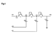
- Fig.4 shows an exemplary implementation of a charge pump comprising npn bipolar transistors T1, T2 and T3.
- An input signal 401 is fed to a node 402.
- the node 402 is connected with the collector and the base of the transistor T1.
- the emitter of the transistor T1 is connected to a node 403.
- the node 403 is connected with the collector and the base of the transistor T2.
- the emitter of the transistor T2 is connected to a node 404.
- the node 404 is connected with the collector and the base of the transistor T3.
- the emitter of the transistor T3 is connected via a capacitor 410 to ground.
- an output signal 405 (e.g. VCP) is supplied via the emitter of the transistor T3.
- a clock signal 406 is supplied via a capacitor 405 to the node 403 and a clock signal 407 is supplied via a capacitor 409 to the node 404.
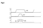
- Fig.5 shows a diagram visualizing voltage transients of a fully overlapping clocking sequence comprising the clock signals 406 and 407 of the circuit according to Fig.4 .
- a signal 501 shows a voltage drop over the transistor T2.
- the maximum voltage drop 502 amounts to one time the clock voltage (which in this example is assumed to have the same value "Vclk" for both clock signals 406 and 407).
- the node 403 When clock signal 406 is high (phase1 in Fig.3 ) the node 403 is charged to Vin + Vclk - VD , wherein Vin is the voltage of the input signal 401, Vclk is the voltage of the clock signal 406 (also the same amount of voltage applies for the clock signal 407) and VD is the voltage drop across the base-emitter diode for each of the transistors, here the transistor T1. Accordingly, the node 404 reaches a voltage amounting to Vin + Vclk - 2 * VD .
- the overlapping clocking scheme as shown in Fig.3 can be generated with a current-source-capacitor based oscillator (CSC oscillator) and additional logic (also referred to as oscillator logic).
- CSC oscillator current-source-capacitor based oscillator
- additional logic also referred to as oscillator logic
- Fig.6 shows a block diagram of an oscillator circuitry comprising a CSC oscillator 601 and an oscillator logic 602, wherein the CSC oscillator 601 conveys a clock signal 603 and a clock signal 604 to the oscillator logic 602, which produces a clock signal 605 and a clock signal 606.
- the CSC oscillator 601 and the oscillator logic 602 are described hereinafter in more detail.
- Fig.7 shows a schematic diagram of the CSC oscillator 601.
- Fig.7 comprises several p-channel MOSFETs MP1 to MP7 and several n-channel MOSFETs MN1 to MN7.
- a node 702 is connected to the gate of the MOSFET MP1 and to the gate of the MOSFET MN1.
- the clock signal 603 is provided via the node 702.
- the drain of the MOSFET MP1 is connected via a current source SC1 to a node 703.
- the bulk of the MOSFET MP1 is connected to the node 703.
- the source of the MOSFET MN1 is connected via a current source SC2 to a node 704.
- the bulk of the MOSFET MN1 is connected to the node 704.
- the source of the MOSFET MP1 is connected to a node 701 and the drain of the MOSFET MN1 is connected to the node 701.
- the node 701 is connected via a capacitor 705 to the node 704.
- the node 701 is connected to the gate of the MOSFET MP6 and to the gate of the MOSFET MN6.
- the source and the bulk of the MOSFET MN6 are connected to the node 704.
- the drain of the MOSFET MN6 is connected to a node 706.
- the source of the MOSFET MP6 is connected to the node 706.
- the drain and the bulk of the MOSFET MP6 are connected to the node 703.
- the node 706 is connected to the gate of the MOSFET MP7 and to the gate of the MOSFET MN7.
- the source and the bulk of the MOSFET MN7 are connected to the node 704.
- the drain and the bulk of the MOSFET MP7 are connected to the node 703.
- the source of the MOSFET MP7 is connected to a node 707 and the drain of the MOSFET MN7 is connected to the node 707.
- the clock signal 604 is provided via the node 707.
- the node 701 is connected to the gates of the MOSFETs MP2, MP3, MN2 and MN3.
- the drain and the bulk of the MOSFET MP2 and the bulk of the MOSFET MP3 are connected to the node 703.
- the source of the MOSFET MP2 and the drain of the MOSFET MP3 are connected to a node 709.
- the node 709 is connected to the drain of the MOSFET MP4.
- the source of the MOSFET MP3 and the drain of the MOSFET MN2 are connected to a node 710.
- the source of the MOSFET MN2 is connected to the drain of the MOSFET MN3.
- the bulk of the MOSFET MN2 is connected to a node 708.
- the bulk and the source of the MOSFET MN3 are connected to the node 708.
- the node 708 is also connected to the node 704.
- the node 708 is connected to the source of the MOSFET MN4.
- the node 710 is connected to the gate of the MOSFET MP4 and to the gate of the MOSFET MN4.
- the node 710 is further connected to the gate of the MOSFET MP5 and to the gate of the MOSFET MN5.
- the bulk and the source of the MOSFET MN5 are connected to the node 704.
- the bulk and the drain of the MOSFET MP5 are connected to the node 703.
- the source of the MOSFET MP5 is connected to the node 702 and the drain of the MOSFET MN5 is connected to the node 702.
- the source of the MOSFET MP4 is connected to the node 704.
- the bulk of the MOSFET MP4 is connected to the node 703.
- the bulk of the MOSFET MN4 is connected to the node 704.
- the drain of the MOSFET MN4 is connected to the node 703.
- the current sources CS1 and CS2 charge and discharge the capacitor 705.
- the transistors MP1 and MN1 act as switches controlling the charging or discharging phase of the capacitor 705 and are switched according to the output signal 603.
- the current sources CS1 and CS2, the switches MP1 and MN1 and the capacitor 705 are dimensioned to realize a maximum admissible frequency (which may be limited by the available or utilized technology).
- Fig.8 shows a resulting voltage transient 801 at a node 701.
- the transistors MP2, MP3, MN2, MN3, MP4 and MN4 are connected in a Schmitt trigger configuration.
- a threshold voltage of the Schmitt trigger is defined by the transistor geometries of MP2, MP3, MN2, MN3, MP4 and MN4.
- a subsequent inverter comprising the transistors MP5 and MN5 provides an inversion of the Schmitt trigger signal and supplies the inverted signal 603.
- Said signal 603 controls the charging and discharging phase of the CSC-element and buffers the Schmitt trigger circuit.
- the transistors MP6, MN6, MP7 and MN7 form two in series connected balanced inverters.
- the first inverter comprising the transistors MP6 and MN6 is directly connected to the node 701.
- the inverters provide switching at the middle of the transition of the charging and discharging phase from the CSC element.
- Fig.9 shows a schematic diagram comprising rectangular signals of the Schmitt trigger and the inverter. Hence, Fig.9 shows at the top the voltage signal 801 at the node 701 in view of the clock signal 603 and the clock signal 604.
- Fig.9 shows a 90°-phase shift between the inverted Schmitt trigger signal (clock signal 603) and the inverter generated signal (clock signal 604). These signals 603 and 604 are logically combined by the oscillator logic 602 to generate the overlapping clock sequence of the clock signals 605 and 606 as also shown in Fig.3 .
- Fig.10 shows a schematic circuit diagram of the oscillator logic 602. Signals from the nodes 703 and 704 are provided to the circuit of Fig.10 as well as the clock signals 603 and 604. Fig.10 also comprises an inverter 1001, an OR gate 1002 and an AND gate 1003. The inverter 1001, the OR gate 1002 and the AND gate 1003 are supplied via connections to the nodes 703 (high supply) and 704 (low supply).
- the clock signal 603 is fed to the inverter 1001, which supplies a signal 1004 via its output, which signal 1004 is fed to the first input of the OR gate 1002.
- the output of the OR gate supplies the clock signal 605.
- the signal 1004 is also fed to the first input of the AND gate 1003.
- the clock signal 604 is conveyed to the second input of the OR gate 1002 and to the second input of the AND gate 1003.
- the output of the AND gate 1003 supplies the clock signal 606.
- the intermediate clock signals 603 and 604 are logically combined to generate an overlapping clock sequence comprising the clock signals 605 and 606, which allows using the bipolar transistors as shown in Fig.4 instead of high voltage transistors.
- Fig.11 shows a signal diagram comprising the clock signals 605 and 606 provided by the circuit of Fig.10 derived from the signals depicted in Fig.9 .
- Fig.12 shows an exemplary circuit diagram that allows generating eight different clocking sequences based on the intermediate clocking signals 603 and 604. According to Fig.10 , the signals from the nodes 703 and 704 are also supplied to the components of Fig.12 as voltage supply lines.
- Fig.12 shows five inverters 1201 to 1205, two OR gates 1206 and 1207 and two AND gates 1208 and 1209.
- the clock signal 603 is conveyed to the inverter 1201, to the second input of the OR gate 1207 and to the second input of the AND gate 1209.
- the clock signal 604 is conveyed to the first input of the OR gate 1207, to the first input of the AND gate 1209, to the second input of the OR gate 1206 and to the second input of the AND gate 1208.
- the output of the inverter 1201 is connected to the first input of the OR gate 1206 and to the first input of the AND gate 1208.
- the output of the OR gate 1206 supplies a clock signal clk1.
- the output of the OR gate 1206 is connected to the inverter 1202, which supplies a clock signal clk6 via its output.
- the output of the AND gate 1208 supplies a clock signal clk2.
- the output of the AND gate 1208 is also connected to the inverter 1203, which supplies a clock signal clk5 via its output.
- the output of the OR gate 1207 supplies a clock signal clk3.
- the output of the OR gate 1207 is connected to the inverter 1204, which supplies a clock signal clk8 via its output.
- the output of the AND gate 1209 supplies a clock signal clk4.
- the output of the AND gate 1207 is also connected to the inverter 1205, which supplies a clock signal clk7 via its output.
- every single clock signal has a phase shift of 90° with regard to the previous clock signal.
- Fig.13 shows a block diagram of an exemplary multi branch charge pump concept.
- the CSC oscillator 601 and the oscillator logic 602 are combined as explained above.
- the oscillator logic 602 supplies eight clock signals clk1 to clk8.
- the clock signals clk1 and clk2 are fed to a two-stage charge pump core 1301 which provides an output signal VCP1.
- the clock signals clk3 and clk4 are fed to a two-stage charge pump core 1302 which provides an output signal VCP2.
- the clock signals clk5 and clk6 are fed to a two-stage charge pump core 1303 which provides an output signal VCP3.
- the clock signals clk7 and clk8 are fed to a two-stage charge pump core 1304 which provides an output signal VCP4.
- the two-stage charge pump cores 1301 to 1304 are supplied via the nodes 703 and 704 (high supply and low supply). Also the output signals VCP1 to VCP4 are combined to an output signal VCP.
- the multi branch charge pump with four charge pump cores as shown in Fig.13 can advantageously overcome frequency limitation of a single charge pump core.
- the resulting frequency may be defined by the base frequency times the number of charge pump cores used.
- an overall behavior can be achieved compared to a charge pump with a single core and a switching frequency amounting to 10MHz.
- Another advantage of the multi branch charge pump concept is a reduced output ripple on the charge pump voltage.
Landscapes
- Engineering & Computer Science (AREA)
- Power Engineering (AREA)
- Dc-Dc Converters (AREA)
Priority Applications (2)
| Application Number | Priority Date | Filing Date | Title |
|---|---|---|---|
| EP20130176466 EP2827483A1 (fr) | 2013-07-15 | 2013-07-15 | Circuit, pompe de charge à branches multiples, procédé de commande d'une pompe de charge et système |
| US14/320,299 US9130451B2 (en) | 2013-07-15 | 2014-06-30 | Circuitry, multi-branch charge pump, method for controlling a charge pump and system |
Applications Claiming Priority (1)
| Application Number | Priority Date | Filing Date | Title |
|---|---|---|---|
| EP20130176466 EP2827483A1 (fr) | 2013-07-15 | 2013-07-15 | Circuit, pompe de charge à branches multiples, procédé de commande d'une pompe de charge et système |
Publications (1)
| Publication Number | Publication Date |
|---|---|
| EP2827483A1 true EP2827483A1 (fr) | 2015-01-21 |
Family
ID=48793936
Family Applications (1)
| Application Number | Title | Priority Date | Filing Date |
|---|---|---|---|
| EP20130176466 Withdrawn EP2827483A1 (fr) | 2013-07-15 | 2013-07-15 | Circuit, pompe de charge à branches multiples, procédé de commande d'une pompe de charge et système |
Country Status (2)
| Country | Link |
|---|---|
| US (1) | US9130451B2 (fr) |
| EP (1) | EP2827483A1 (fr) |
Citations (6)
| Publication number | Priority date | Publication date | Assignee | Title |
|---|---|---|---|---|
| US5258662A (en) * | 1992-04-06 | 1993-11-02 | Linear Technology Corp. | Micropower gate charge pump for power MOSFETS |
| US5774012A (en) * | 1995-09-14 | 1998-06-30 | Samsung Electronics, Co., Ltd. | Charge-pumping circuit for semiconductor memory device |
| US6026002A (en) * | 1996-03-28 | 2000-02-15 | Siemens Aktiengesellschaft | Circuit configuration for supplying an electronic load circuit |
| US20070096796A1 (en) * | 2005-08-26 | 2007-05-03 | Firmansyah Teezar R | High voltage charge pump with wide range of supply voltage |
| JP2011062006A (ja) * | 2009-09-11 | 2011-03-24 | Murata Mfg Co Ltd | 昇圧回路 |
| EP2538534A1 (fr) * | 2011-06-06 | 2012-12-26 | Sharp Kabushiki Kaisha | Circuit dýalimentation électrique de commutation, dispositif semi-conducteur et dispositif d'éclairage à DEL |
Family Cites Families (10)
| Publication number | Priority date | Publication date | Assignee | Title |
|---|---|---|---|---|
| IT1225608B (it) * | 1988-07-06 | 1990-11-22 | Sgs Thomson Microelectronics | Regolazione della tensione prodotta da un moltiplicatore di tensione. |
| JP3643385B2 (ja) * | 1993-05-19 | 2005-04-27 | 株式会社東芝 | 半導体回路装置 |
| US5793246A (en) * | 1995-11-08 | 1998-08-11 | Altera Corporation | High voltage pump scheme incorporating an overlapping clock |
| US5818766A (en) * | 1997-03-05 | 1998-10-06 | Integrated Silicon Solution Inc. | Drain voltage pump circuit for nonvolatile memory device |
| DE19748577C1 (de) * | 1997-11-04 | 1999-01-21 | Bosch Gmbh Robert | Ladungspumpe |
| EP1014547A3 (fr) * | 1998-12-21 | 2000-11-15 | Fairchild Semiconductor Corporation | Système de pompe de charge à courant bas |
| KR20030072527A (ko) * | 2002-03-04 | 2003-09-15 | 주식회사 엘지이아이 | 직류-직류 컨버터의 발진기 |
| US6891764B2 (en) * | 2003-04-11 | 2005-05-10 | Intel Corporation | Apparatus and method to read a nonvolatile memory |
| KR100716661B1 (ko) * | 2005-03-31 | 2007-05-09 | 주식회사 하이닉스반도체 | 전압 부스터 회로 |
| US7342438B2 (en) * | 2006-06-29 | 2008-03-11 | Intel Corporation | N-channel negative charge pump |
-
2013
- 2013-07-15 EP EP20130176466 patent/EP2827483A1/fr not_active Withdrawn
-
2014
- 2014-06-30 US US14/320,299 patent/US9130451B2/en active Active
Patent Citations (6)
| Publication number | Priority date | Publication date | Assignee | Title |
|---|---|---|---|---|
| US5258662A (en) * | 1992-04-06 | 1993-11-02 | Linear Technology Corp. | Micropower gate charge pump for power MOSFETS |
| US5774012A (en) * | 1995-09-14 | 1998-06-30 | Samsung Electronics, Co., Ltd. | Charge-pumping circuit for semiconductor memory device |
| US6026002A (en) * | 1996-03-28 | 2000-02-15 | Siemens Aktiengesellschaft | Circuit configuration for supplying an electronic load circuit |
| US20070096796A1 (en) * | 2005-08-26 | 2007-05-03 | Firmansyah Teezar R | High voltage charge pump with wide range of supply voltage |
| JP2011062006A (ja) * | 2009-09-11 | 2011-03-24 | Murata Mfg Co Ltd | 昇圧回路 |
| EP2538534A1 (fr) * | 2011-06-06 | 2012-12-26 | Sharp Kabushiki Kaisha | Circuit dýalimentation électrique de commutation, dispositif semi-conducteur et dispositif d'éclairage à DEL |
Non-Patent Citations (1)
| Title |
|---|
| "Smart Power ICs: Technologies and Applications", 2002, SPRINGER-VERLAG |
Also Published As
| Publication number | Publication date |
|---|---|
| US20150015324A1 (en) | 2015-01-15 |
| US9130451B2 (en) | 2015-09-08 |
Similar Documents
| Publication | Publication Date | Title |
|---|---|---|
| US10003258B2 (en) | Charge pump circuit with a low reverse current | |
| US7388422B2 (en) | Charge pump circuit for high side drive circuit and driver driving voltage circuit | |
| US7495482B2 (en) | Semiconductor device | |
| US9966871B2 (en) | Rectification device, alternator, and power conversion device | |
| US9806616B2 (en) | Control circuit for multiple high side switches | |
| US8456225B1 (en) | Negative charge pump | |
| CN101826794A (zh) | 逆流防止电路以及电源切换装置 | |
| US9954519B2 (en) | Electronic switch, and corresponding device and method | |
| KR101297460B1 (ko) | 게이트 구동 장치 | |
| US10756728B2 (en) | Insulated gate device drive apparatus | |
| CN102208898A (zh) | 差动放大电路 | |
| US20030231046A1 (en) | High voltage level shifting IC with under-ground voltage swing withstanding capability | |
| US10218351B2 (en) | Parallel driving circuit of voltage-driven type semiconductor element | |
| US7733135B2 (en) | High side boosted gate drive circuit | |
| US9595967B2 (en) | Level shift circuit and driver circuit | |
| JP2005304218A (ja) | 電源ドライバ装置及びスイッチング電源装置 | |
| CN101542905B (zh) | 反相器电路 | |
| TW201709650A (zh) | 電荷幫浦電路及使用其的馬達驅動電路 | |
| EP2827483A1 (fr) | Circuit, pompe de charge à branches multiples, procédé de commande d'une pompe de charge et système | |
| US7102416B2 (en) | High side switching circuit | |
| JP2007129828A (ja) | チャージポンプ回路 | |
| CN108696118B (zh) | 增压电路及其中的基体的偏压方法 | |
| JP3794481B2 (ja) | 負荷駆動回路および負荷駆動回路を有する半導体装置 | |
| JP4281360B2 (ja) | チャージポンプ回路 | |
| WO2021085027A1 (fr) | Circuit d'attaque de grille |
Legal Events
| Date | Code | Title | Description |
|---|---|---|---|
| 17P | Request for examination filed |
Effective date: 20130715 |
|
| AK | Designated contracting states |
Kind code of ref document: A1 Designated state(s): AL AT BE BG CH CY CZ DE DK EE ES FI FR GB GR HR HU IE IS IT LI LT LU LV MC MK MT NL NO PL PT RO RS SE SI SK SM TR |
|
| AX | Request for extension of the european patent |
Extension state: BA ME |
|
| PUAI | Public reference made under article 153(3) epc to a published international application that has entered the european phase |
Free format text: ORIGINAL CODE: 0009012 |
|
| STAA | Information on the status of an ep patent application or granted ep patent |
Free format text: STATUS: THE APPLICATION IS DEEMED TO BE WITHDRAWN |
|
| 18D | Application deemed to be withdrawn |
Effective date: 20150722 |