EP0032588A2 - Circuit générateur de polarisation de substrat - Google Patents
Circuit générateur de polarisation de substrat Download PDFInfo
- Publication number
- EP0032588A2 EP0032588A2 EP80108185A EP80108185A EP0032588A2 EP 0032588 A2 EP0032588 A2 EP 0032588A2 EP 80108185 A EP80108185 A EP 80108185A EP 80108185 A EP80108185 A EP 80108185A EP 0032588 A2 EP0032588 A2 EP 0032588A2
- Authority
- EP
- European Patent Office
- Prior art keywords
- circuit
- substrate bias
- mos transistor
- voltage
- coupled
- Prior art date
- Legal status (The legal status is an assumption and is not a legal conclusion. Google has not performed a legal analysis and makes no representation as to the accuracy of the status listed.)
- Granted
Links
Images

Classifications
-
- G—PHYSICS
- G05—CONTROLLING; REGULATING
- G05F—SYSTEMS FOR REGULATING ELECTRIC OR MAGNETIC VARIABLES
- G05F3/00—Non-retroactive systems for regulating electric variables by using an uncontrolled element, or an uncontrolled combination of elements, such element or such combination having self-regulating properties
- G05F3/02—Regulating voltage or current
- G05F3/08—Regulating voltage or current wherein the variable is dc
- G05F3/10—Regulating voltage or current wherein the variable is dc using uncontrolled devices with non-linear characteristics
- G05F3/16—Regulating voltage or current wherein the variable is dc using uncontrolled devices with non-linear characteristics being semiconductor devices
- G05F3/20—Regulating voltage or current wherein the variable is dc using uncontrolled devices with non-linear characteristics being semiconductor devices using diode- transistor combinations
- G05F3/205—Substrate bias-voltage generators
Definitions
- This invention relates to a substrate bias generation circuit producing stable substrate bias.
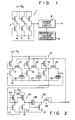
- a substrate bias generation circuit as shown in Fig. 1, for example, is formed on the same substrate that carries the integrated circuit in order to apply a given substrate bias voltage to the substrate.
- This substrate bias generation circuit includes a ring oscillator formed of three cascade-connected MOS inverters 2, 4 and 6, the output terminal of the last-stage MOS inverter 6 being coupled to the input terminal of the first-stage MOS inverter 2, and a charge pump circuit 8 which is to be energized by a reference voltage from a reference voltage generator 9 to pump negative electric charges into the substrate in accordance with an output signal from the oscillator 1, thereby applying a negative bias voltage V B to the substrate.
- the substrate bias generation circuit of this type is formed on the same substrate with a memory or logic circuit, a leakage current will possibly flow into the substrate to lower the substrate voltage while the memory or lcgic circuit is operating.
- the substrate voltage is restored to a predetermined voltage level by the charge pump function of the charge pump circuit 8, it requires a considerably long time for the predetermined substrate voltage to be established .again. Accordingly, the substrate voltage will possibly fluctuate during the operation of the memory circuit or the like to exert an unnecessary influence upon the operation of the memory circuit.
- the object of this invention is to provide a substrate bias generation circuit capable of producing stable substrate bias, with the charge pump speed changed in accordance with the.variation of the substrate voltage.
- a substrate bias generation circuit which comprises a voltage-controlled oscillator circuit, a driving circuit producing a driving signal in accordance with an oscillation output signal from the oscillator circuit, and a charge pump circuit producing a substrate bias voltage in accordance with the driving signal from the driving circuit, the substrate bias voltage from the charge pump circuit being supplied also to a control terminal of the voltage-controlled oscillator circuit.
- the oscillation frequency of the voltage-controlled oscillator circuit is increased in response to the drop of the substrate voltage, so that the charge pump circuit pumps charges into the substrate at a higher rate.
- the substrate voltage is immediately restored to a predetermined voltage level, and the influence of the fluctuation of the substrate voltage upon the main circuit may substantially be minimized.
- a substrate bias generation circuit includes a voltage-controlled oscillator circuit 10, a driving circuit 20 producing a pulse signal at a rate corresponding to an oscillation output signal from the oscillator circuit 10, and a charge pump circuit 30 for pumping electric charges into a substrate in accordance with a pulse output signal from the driving circuit 20.
- the voltage-controlled oscillator circuit 10 is formed of a ring oscillator including three MOS inverters 11, 12 and 13 which are each composed of a depression-type (D-type) MOS transistor and an enhancement-type (E-type) MOS transistor coupled in series between a power supply terminal V D and the ground.
- MOS inverters 11, 12 and 13 which are each composed of a depression-type (D-type) MOS transistor and an enhancement-type (E-type) MOS transistor coupled in series between a power supply terminal V D and the ground.
- the output terminal of the MOS inverter 11 is coupled to the input terminal of the MOS inverter 12 through a delay circuit which is formed of a D-type MOS transistor 14 and an MOS capacitor 15, the output terminal of the MOS inverter 12 is coupled to the input terminal of the MOS inverter 13 through a delay circuit which is formed of a D-type MOS transistor 16 and an MOS capacitor 17, and the output terminal of the MOS inverter 13 is coupled to the input terminal of the MOS inverter 11 through a delay circuit which is formed of a D-type MOS transistor 18 and an MOS capacitor 19.
- the driving circuit 20 includes E-type MOS transistors 21 and 22 having their gates coupled with the output terminal of the MOS inverter 13 of the ring oscillator 10 and their sources grounded, and D-type MOS transistors 23 and 24 having their sources coupled respectively with the drains of the E-type MOS transistors 21 and 22 and their drains connected to the power supply terminal V D .
- the source of the MOS transistor 23 is coupled with the gates of the MOS transistors 23 and 24.
- the charge pump circuit 30 includes an E-type MOS transistor 31 having its gate coupled with the drain of the MOS transistor 22 of the driving circuit 20 and its source grounded, an MOS capacitor 32 coupled between the gate and drain of the MOS transistor 31, and an E-type MOS transistor 33 having its source coupled with the drain of the MOS transistor 31.
- the gate and drain of the MOS transistor 33 are both coupled with the gates of the MOS transistors 14, 16 and 18 of the ring oscillator 10.
- Figs. 3A and 3B there will be described the operation of the substrate bias generation circuit shown in Fig. 2.
- the ring oscillator 10 When supply voltage is applied to the power supply terminal V DY the ring oscillator 10 produces an oscillator output signal of frequency f o , as shown in Fig. 3A, if the substrate bias generator circuit operates normally.
- the MOS transistors 21 and 22 are caused to conduct in response to a positive half-cycle output signal component from the ring oscillator 10, and a low-level output signal is generated from the driving circuit 20. If a negative half-cycle output signal component is generated from the ring oscillator 10, then the MOS transistors 21 and 22 are rendered nonconductive, and a high-level output signal is generated from the driving circuit 20. Namely, the driving circuit 20 produces a pulse signal of frequency f o in response to the oscillation output signal of frequency f o from the ring oscillator 10.
- the MOS transistors 31 and 33 of the charge pump circuit 30 are turned on and off, respectively. In this case, therefore, electric charges of an amount corresponding to the supply voltage are stored in the MOS capacitor 32. Thereafter, when the low-level output signal is generated from the driving circuit 20, the MOS transistors 31 and.33 are turned off and on, respectively. Thus, the positive charges stored in the MOS capacitor 32 are discharged through the MOS transistor 22, and the negative charges are pumped into the substrate (not shown) through the MOS transistor 33. In this way, a substrate bias voltage V B is maintained at a predetermined level V BO by the charge pumping action of the charge pump circuit 30, as shown in Fig. 3B.
- the absolute value of the substrate bias voltage V B is reduced at time t, by an operating current caused to flow at the time of an operation of e.g. a memory circuit (not shown) formed on the substrate, as shown in Fig. 3B.
- the absolute values of the gate voltages of the MOS transistors 14, 16 and 18 of the ring oscillator 10 are reduced to diminish the resistance values of these MOS transistors 14, 16 and 18, thereby decreasing the time constants of the delay circuits in which the MOS transistors 14, 16 and 18 cooperate with the MOS capacitors 15, 17 and 19. Accordingly, 'the oscillation frequency of the ring oscillator 10 increases as shown in Fig. 3A.
- the driving circuit 20 when an oscillation output signal with a higher frequency than the frequency f o is generated from the ring oscillator 10, the driving circuit 20 produces pulse signals at a higher rate to drive the charge pump circuit 30 at a higher operating speed. As a result, a large quantity of negative charges are pumped into the substrate in a short time to bring the substrate potential close to the predetermined level V BO as shown in Fig. 3B. As the absolute value of the substrate potential VB increases, the conduction resistances of the MOS transistors 14, 16 and 18 increase gradually. When the substrate potential VB reach the predetermined level V B0 , the ring oscillator 10 again executes the oscillating operation at the predetermined.frequency f o .
- the oscillation frequency of the ring oscillator 10 is increased to raise the operating speed of the charge pump circuit 30 when the substrate potential VB is reduced so that the substrate potential VB may instantaneously be restored to the predetermined level VBO . Accordingly, the influence of the change of the substrate potential caused by the operating current flow at the time of the operation of the memory circuit or the like upon the operation of the memory circuit can be ignored.
- the charge pump circuit 30 When the charge pump circuit 30 operates at a high speed, that is, when the absolute value of the substrate voltage V B is reduced, the current consumed in the ring oscillator 10 is relatively great. When the charge pump circuit 30 operates normally, that is, when the substrate voltage V B is maintained at the predetermined level VBO . however, the consumption current in the ring oscillator 10 can be minimized.
- the MOS inverters 11, 12 and 13 constituting the ring oscillator 10 may also be each formed of two series-connected E-type MOS transistors. Further, the-ring oscillator 10 may also be formed of a single or an odd number of MOS inverters. Moreover, where the oscillation frequency of the ring oscillator 10 can be changed within a desired range by controlling the resistance values of the load MOS transistors of the MOS inverters 11, 12 and 13 by means of the substrate bias voltage, the delay circuits formed of the MOS transistors 14, 16 and 18 and the MOS capacitors 15, 17 and 19 may be removed.
- N-channel MOS transistors are used in the substrate bias generation circuit shown in Fig. 2, P-channel MOS transistors may be used instead.
- the.MOS capacitors 19, 15 and 17 may be removed if the gate capacities of the switching MOS transistors.of the MOS inverters 11, 12 and 13 are great enough.
- MOS transistors 114, 116 and 118 may be coupled between the load MOS transistors of the MOS inverters 11, 12 and 13 and the power supply terminal VD instead of using the transistors 14, 16 and 18 which constitute the delay circuits.
- the MOS transistors 114, 116 and 118 are directly coupled in series with the MOS capacitors 15, 17 and 19, respectively, between the power supply terminal VD and the ground to form delay circuits.
Landscapes
- Engineering & Computer Science (AREA)
- Physics & Mathematics (AREA)
- Microelectronics & Electronic Packaging (AREA)
- Nonlinear Science (AREA)
- Electromagnetism (AREA)
- General Physics & Mathematics (AREA)
- Radar, Positioning & Navigation (AREA)
- Automation & Control Theory (AREA)
- Semiconductor Integrated Circuits (AREA)
- Dram (AREA)
Applications Claiming Priority (2)
| Application Number | Priority Date | Filing Date | Title |
|---|---|---|---|
| JP17165779A JPS5694654A (en) | 1979-12-27 | 1979-12-27 | Generating circuit for substrate bias voltage |
| JP171657/79 | 1979-12-27 |
Publications (3)
| Publication Number | Publication Date |
|---|---|
| EP0032588A2 true EP0032588A2 (fr) | 1981-07-29 |
| EP0032588A3 EP0032588A3 (en) | 1981-08-05 |
| EP0032588B1 EP0032588B1 (fr) | 1986-04-23 |
Family
ID=15927272
Family Applications (1)
| Application Number | Title | Priority Date | Filing Date |
|---|---|---|---|
| EP80108185A Expired EP0032588B1 (fr) | 1979-12-27 | 1980-12-23 | Circuit générateur de polarisation de substrat |
Country Status (4)
| Country | Link |
|---|---|
| US (1) | US4388537A (fr) |
| EP (1) | EP0032588B1 (fr) |
| JP (1) | JPS5694654A (fr) |
| DE (1) | DE3071578D1 (fr) |
Cited By (11)
| Publication number | Priority date | Publication date | Assignee | Title |
|---|---|---|---|---|
| EP0029681A2 (fr) * | 1979-11-22 | 1981-06-03 | Fujitsu Limited | Générateur de tension de polarisation |
| EP0118108A2 (fr) * | 1983-03-04 | 1984-09-12 | Nec Corporation | Mémoire à accès aléatoire avec mode d'opération actif et mode d'opération d'attente |
| FR2555774A1 (fr) * | 1983-11-30 | 1985-05-31 | Ates Componenti Elettron | Circuit regulateur de la tension de polarisation du substrat d'un circuit integre a transistors a effet de champ |
| EP0143879A1 (fr) * | 1983-10-27 | 1985-06-12 | International Business Machines Corporation | Génerateur de tension de substrat |
| GB2161664A (en) * | 1984-05-30 | 1986-01-15 | Hitachi Ltd | Semiconductor device having preventive means against errors |
| EP0386282A1 (fr) * | 1989-03-06 | 1990-09-12 | Siemens Aktiengesellschaft | Source de tension de référence intégrée |
| EP0449235A2 (fr) * | 1990-03-26 | 1991-10-02 | Micron Technology, Inc. | Circuit de pompe à charge à haute efficacité |
| EP0477108A2 (fr) * | 1990-09-20 | 1992-03-25 | Fujitsu Limited | Générateur de tension pour un circuit intégré à semi-conducteur |
| GB2256950A (en) * | 1991-06-17 | 1992-12-23 | Samsung Electronics Co Ltd | Sensing and controlling substrate voltage level |
| EP0599275A1 (fr) * | 1992-11-27 | 1994-06-01 | Nec Corporation | Circuit intégré semi-conducteur comportant un circuit de retard avec une caractéristique tension-retard proportionelle à la tension d'alimentation |
| EP0663668A2 (fr) * | 1993-09-29 | 1995-07-19 | Texas Instruments Deutschland Gmbh | Améliorations concernant EEPROMs |
Families Citing this family (40)
| Publication number | Priority date | Publication date | Assignee | Title |
|---|---|---|---|---|
| DE3171351D1 (en) * | 1980-12-22 | 1985-08-14 | British Telecomm | Improvements in or relating to electronic clock generators |
| JPS57208251A (en) * | 1981-06-19 | 1982-12-21 | Canon Inc | Ink jet head |
| JPS57186351A (en) * | 1981-05-12 | 1982-11-16 | Fujitsu Ltd | Semiconductor device |
| JPS57199335A (en) * | 1981-06-02 | 1982-12-07 | Toshiba Corp | Generating circuit for substrate bias |
| JPS57204640A (en) * | 1981-06-12 | 1982-12-15 | Fujitsu Ltd | Generating circuit of substrate bias voltage |
| US4439692A (en) * | 1981-12-07 | 1984-03-27 | Signetics Corporation | Feedback-controlled substrate bias generator |
| US4433253A (en) * | 1981-12-10 | 1984-02-21 | Standard Microsystems Corporation | Three-phase regulated high-voltage charge pump |
| JPS58118135A (ja) * | 1982-01-06 | 1983-07-14 | Hitachi Ltd | ダイナミック型ram |
| US4513427A (en) * | 1982-08-30 | 1985-04-23 | Xerox Corporation | Data and clock recovery system for data communication controller |
| US4494021A (en) * | 1982-08-30 | 1985-01-15 | Xerox Corporation | Self-calibrated clock and timing signal generator for MOS/VLSI circuitry |
| US4585954A (en) * | 1983-07-08 | 1986-04-29 | Texas Instruments Incorporated | Substrate bias generator for dynamic RAM having variable pump current level |
| US4590389A (en) * | 1984-04-02 | 1986-05-20 | Motorola Inc. | Compensation circuit and method for stabilization of a circuit node by multiplication of displacement current |
| US4631421A (en) * | 1984-08-14 | 1986-12-23 | Texas Instruments | CMOS substrate bias generator |
| US4656369A (en) * | 1984-09-17 | 1987-04-07 | Texas Instruments Incorporated | Ring oscillator substrate bias generator with precharge voltage feedback control |
| JPS6445157A (en) * | 1987-08-13 | 1989-02-17 | Toshiba Corp | Semiconductor integrated circuit |
| US5003197A (en) * | 1989-01-19 | 1991-03-26 | Xicor, Inc. | Substrate bias voltage generating and regulating apparatus |
| JP2841480B2 (ja) * | 1989-06-21 | 1998-12-24 | 日本電気株式会社 | 基板電位設定回路 |
| US5132936A (en) * | 1989-12-14 | 1992-07-21 | Cypress Semiconductor Corporation | MOS memory circuit with fast access time |
| JPH0494566A (ja) * | 1990-08-10 | 1992-03-26 | Sharp Corp | 半導体記憶装置の基板バイアス発生回路 |
| US5519654A (en) * | 1990-09-17 | 1996-05-21 | Kabushiki Kaisha Toshiba | Semiconductor memory device with external capacitor to charge pump in an EEPROM circuit |
| US5081429A (en) * | 1991-03-29 | 1992-01-14 | Codex Corp. | Voltage controlled oscillator with controlled load |
| US5168174A (en) * | 1991-07-12 | 1992-12-01 | Texas Instruments Incorporated | Negative-voltage charge pump with feedback control |
| US5295095A (en) * | 1991-08-22 | 1994-03-15 | Lattice Semiconductor Corporation | Method of programming electrically erasable programmable read-only memory using particular substrate bias |
| JP2998944B2 (ja) * | 1991-12-19 | 2000-01-17 | シャープ株式会社 | リングオシレータ |
| US5412257A (en) * | 1992-10-20 | 1995-05-02 | United Memories, Inc. | High efficiency N-channel charge pump having a primary pump and a non-cascaded secondary pump |
| US5446367A (en) * | 1993-05-25 | 1995-08-29 | Micron Semiconductor, Inc. | Reducing current supplied to an integrated circuit |
| US5365204A (en) * | 1993-10-29 | 1994-11-15 | International Business Machines Corporation | CMOS voltage controlled ring oscillator |
| WO1996028850A1 (fr) * | 1995-03-09 | 1996-09-19 | Macronix International Co., Ltd. | Pompe de charge pour condensateurs montes en serie |
| FR2773019B1 (fr) * | 1997-12-24 | 2001-10-12 | Sgs Thomson Microelectronics | Dispositif de generation d'une impulsion de tension |
| JP2000069603A (ja) * | 1998-08-24 | 2000-03-03 | Mitsubishi Heavy Ind Ltd | バッテリ車両の回生制動装置 |
| US6933769B2 (en) * | 2003-08-26 | 2005-08-23 | Micron Technology, Inc. | Bandgap reference circuit |
| US7719343B2 (en) * | 2003-09-08 | 2010-05-18 | Peregrine Semiconductor Corporation | Low noise charge pump method and apparatus |
| US7888962B1 (en) | 2004-07-07 | 2011-02-15 | Cypress Semiconductor Corporation | Impedance matching circuit |
| US8072834B2 (en) * | 2005-08-25 | 2011-12-06 | Cypress Semiconductor Corporation | Line driver circuit and method with standby mode of operation |
| US8036846B1 (en) | 2005-10-20 | 2011-10-11 | Cypress Semiconductor Corporation | Variable impedance sense architecture and method |
| US9660590B2 (en) | 2008-07-18 | 2017-05-23 | Peregrine Semiconductor Corporation | Low-noise high efficiency bias generation circuits and method |
| US8816659B2 (en) | 2010-08-06 | 2014-08-26 | Peregrine Semiconductor Corporation | Low-noise high efficiency bias generation circuits and method |
| JP2011528870A (ja) * | 2008-07-18 | 2011-11-24 | ペレグリン セミコンダクター コーポレーション | 低ノイズ高効率バイアス生成回路及び方法 |
| US8686787B2 (en) | 2011-05-11 | 2014-04-01 | Peregrine Semiconductor Corporation | High voltage ring pump with inverter stages and voltage boosting stages |
| US9264053B2 (en) | 2011-01-18 | 2016-02-16 | Peregrine Semiconductor Corporation | Variable frequency charge pump |
Citations (4)
| Publication number | Priority date | Publication date | Assignee | Title |
|---|---|---|---|---|
| US3806741A (en) * | 1972-05-17 | 1974-04-23 | Standard Microsyst Smc | Self-biasing technique for mos substrate voltage |
| FR2333296A1 (fr) * | 1975-11-28 | 1977-06-24 | Honeywell Inf Systems | Tension de polarisation de substrat engendree par oscillateur de regeneration |
| US4142114A (en) * | 1977-07-18 | 1979-02-27 | Mostek Corporation | Integrated circuit with threshold regulation |
| EP0015342A1 (fr) * | 1979-03-05 | 1980-09-17 | Motorola, Inc. | Régulateur de polarisation de substrat |
Family Cites Families (2)
| Publication number | Priority date | Publication date | Assignee | Title |
|---|---|---|---|---|
| US4115710A (en) * | 1976-12-27 | 1978-09-19 | Texas Instruments Incorporated | Substrate bias for MOS integrated circuit |
| US4208595A (en) * | 1978-10-24 | 1980-06-17 | International Business Machines Corporation | Substrate generator |
-
1979
- 1979-12-27 JP JP17165779A patent/JPS5694654A/ja active Granted
-
1980
- 1980-12-03 US US06/212,520 patent/US4388537A/en not_active Expired - Lifetime
- 1980-12-23 DE DE8080108185T patent/DE3071578D1/de not_active Expired
- 1980-12-23 EP EP80108185A patent/EP0032588B1/fr not_active Expired
Patent Citations (4)
| Publication number | Priority date | Publication date | Assignee | Title |
|---|---|---|---|---|
| US3806741A (en) * | 1972-05-17 | 1974-04-23 | Standard Microsyst Smc | Self-biasing technique for mos substrate voltage |
| FR2333296A1 (fr) * | 1975-11-28 | 1977-06-24 | Honeywell Inf Systems | Tension de polarisation de substrat engendree par oscillateur de regeneration |
| US4142114A (en) * | 1977-07-18 | 1979-02-27 | Mostek Corporation | Integrated circuit with threshold regulation |
| EP0015342A1 (fr) * | 1979-03-05 | 1980-09-17 | Motorola, Inc. | Régulateur de polarisation de substrat |
Non-Patent Citations (1)
| Title |
|---|
| PATENTS ABSTRACTS OF JAPAN, vol. 2, no. 134, November 9, 1978, page 8332 E 78 * |
Cited By (19)
| Publication number | Priority date | Publication date | Assignee | Title |
|---|---|---|---|---|
| EP0029681A2 (fr) * | 1979-11-22 | 1981-06-03 | Fujitsu Limited | Générateur de tension de polarisation |
| EP0029681A3 (en) * | 1979-11-22 | 1983-01-26 | Fujitsu Limited | Bias-voltage generator |
| EP0118108A2 (fr) * | 1983-03-04 | 1984-09-12 | Nec Corporation | Mémoire à accès aléatoire avec mode d'opération actif et mode d'opération d'attente |
| EP0118108A3 (en) * | 1983-03-04 | 1988-02-03 | Nec Corporation | Random access memory having active and standby modes |
| EP0143879A1 (fr) * | 1983-10-27 | 1985-06-12 | International Business Machines Corporation | Génerateur de tension de substrat |
| FR2555774A1 (fr) * | 1983-11-30 | 1985-05-31 | Ates Componenti Elettron | Circuit regulateur de la tension de polarisation du substrat d'un circuit integre a transistors a effet de champ |
| GB2151823A (en) * | 1983-11-30 | 1985-07-24 | Ates Componenti Elettron | Polarization voltage regulating circuit for field-effect transistor integrated circuit substrate |
| GB2161664A (en) * | 1984-05-30 | 1986-01-15 | Hitachi Ltd | Semiconductor device having preventive means against errors |
| EP0386282A1 (fr) * | 1989-03-06 | 1990-09-12 | Siemens Aktiengesellschaft | Source de tension de référence intégrée |
| EP0449235A2 (fr) * | 1990-03-26 | 1991-10-02 | Micron Technology, Inc. | Circuit de pompe à charge à haute efficacité |
| EP0449235A3 (en) * | 1990-03-26 | 1992-09-02 | Micron Technology, Inc. | High efficiency charge pump circuit |
| EP0477108A2 (fr) * | 1990-09-20 | 1992-03-25 | Fujitsu Limited | Générateur de tension pour un circuit intégré à semi-conducteur |
| EP0477108A3 (en) * | 1990-09-20 | 1992-07-08 | Fujitsu Limited | Voltage generator for a semiconductor integrated circuit |
| US5227675A (en) * | 1990-09-20 | 1993-07-13 | Fujitsu Limited | Voltage generator for a semiconductor integrated circuit |
| GB2256950A (en) * | 1991-06-17 | 1992-12-23 | Samsung Electronics Co Ltd | Sensing and controlling substrate voltage level |
| EP0599275A1 (fr) * | 1992-11-27 | 1994-06-01 | Nec Corporation | Circuit intégré semi-conducteur comportant un circuit de retard avec une caractéristique tension-retard proportionelle à la tension d'alimentation |
| US5461585A (en) * | 1992-11-27 | 1995-10-24 | Nec Corporation | Semiconductor integrated circuit having delay circuit with voltage-to-delay characteristics proportional to power voltage level |
| EP0663668A2 (fr) * | 1993-09-29 | 1995-07-19 | Texas Instruments Deutschland Gmbh | Améliorations concernant EEPROMs |
| EP0663668A3 (fr) * | 1993-09-29 | 1996-07-10 | Texas Instruments Deutschland | Améliorations concernant EEPROMs. |
Also Published As
| Publication number | Publication date |
|---|---|
| DE3071578D1 (en) | 1986-05-28 |
| JPH0114712B2 (fr) | 1989-03-14 |
| EP0032588B1 (fr) | 1986-04-23 |
| EP0032588A3 (en) | 1981-08-05 |
| US4388537A (en) | 1983-06-14 |
| JPS5694654A (en) | 1981-07-31 |
Similar Documents
| Publication | Publication Date | Title |
|---|---|---|
| US4388537A (en) | Substrate bias generation circuit | |
| US4739191A (en) | Depletion-mode FET for the regulation of the on-chip generated substrate bias voltage | |
| EP0735677B1 (fr) | Circuit oscillateur ayant une fréquence d'oscillation indépendante de la tension d'alimentation | |
| US4891609A (en) | Ring oscillator | |
| KR100374644B1 (ko) | 승압 전압의 조절이 가능한 전압 승압 회로 | |
| US5208557A (en) | Multiple frequency ring oscillator | |
| US4236199A (en) | Regulated high voltage power supply | |
| US4387350A (en) | Watch circuit with oscillator gain control | |
| WO1990008426A1 (fr) | Appareil generateur et regulateur de tension de polarisation de substrat | |
| EP0086090B1 (fr) | Circuit d'attaque pour charges capacitives | |
| US5898336A (en) | Charging pump circuit and a phase-locked loop circuit using the same | |
| US6300839B1 (en) | Frequency controlled system for positive voltage regulation | |
| US6373311B1 (en) | Oscillator and switch-over control circuit for a high-voltage generator | |
| EP0174694A1 (fr) | Circuit générant une tension de polarisation de substrat | |
| US4433253A (en) | Three-phase regulated high-voltage charge pump | |
| US5705946A (en) | Low power low voltage level shifter | |
| US10476383B2 (en) | Negative charge pump circuit | |
| KR0132781B1 (ko) | 최소한 하나의 푸쉬-풀 단을 갖는 집적회로 | |
| US4472645A (en) | Clock circuit for generating non-overlapping pulses | |
| US6271735B1 (en) | Oscillator controller with first and second voltage reference | |
| US5563548A (en) | Output voltage controlling circuit in a negative charge pump | |
| JP3087683B2 (ja) | 電圧制御発振回路 | |
| US5146109A (en) | Circuit for driving a floating circuit in response to a digital signal | |
| KR100745857B1 (ko) | 전자 회로 | |
| US6060955A (en) | Voltage compensated oscillator and method therefor |
Legal Events
| Date | Code | Title | Description |
|---|---|---|---|
| PUAI | Public reference made under article 153(3) epc to a published international application that has entered the european phase |
Free format text: ORIGINAL CODE: 0009012 |
|
| PUAL | Search report despatched |
Free format text: ORIGINAL CODE: 0009013 |
|
| AK | Designated contracting states |
Designated state(s): DE FR GB NL |
|
| AK | Designated contracting states |
Designated state(s): DE FR GB NL |
|
| 17P | Request for examination filed |
Effective date: 19801223 |
|
| RAP1 | Party data changed (applicant data changed or rights of an application transferred) |
Owner name: KABUSHIKI KAISHA TOSHIBA |
|
| GRAA | (expected) grant |
Free format text: ORIGINAL CODE: 0009210 |
|
| AK | Designated contracting states |
Kind code of ref document: B1 Designated state(s): DE FR GB NL |
|
| REF | Corresponds to: |
Ref document number: 3071578 Country of ref document: DE Date of ref document: 19860528 |
|
| ET | Fr: translation filed | ||
| PLBE | No opposition filed within time limit |
Free format text: ORIGINAL CODE: 0009261 |
|
| STAA | Information on the status of an ep patent application or granted ep patent |
Free format text: STATUS: NO OPPOSITION FILED WITHIN TIME LIMIT |
|
| 26N | No opposition filed | ||
| PGFP | Annual fee paid to national office [announced via postgrant information from national office to epo] |
Ref country code: FR Payment date: 19941209 Year of fee payment: 15 |
|
| PGFP | Annual fee paid to national office [announced via postgrant information from national office to epo] |
Ref country code: GB Payment date: 19941213 Year of fee payment: 15 |
|
| PGFP | Annual fee paid to national office [announced via postgrant information from national office to epo] |
Ref country code: DE Payment date: 19941222 Year of fee payment: 15 |
|
| PGFP | Annual fee paid to national office [announced via postgrant information from national office to epo] |
Ref country code: NL Payment date: 19941231 Year of fee payment: 15 |
|
| PG25 | Lapsed in a contracting state [announced via postgrant information from national office to epo] |
Ref country code: GB Effective date: 19951223 |
|
| PG25 | Lapsed in a contracting state [announced via postgrant information from national office to epo] |
Ref country code: NL Effective date: 19960701 |
|
| GBPC | Gb: european patent ceased through non-payment of renewal fee |
Effective date: 19951223 |
|
| PG25 | Lapsed in a contracting state [announced via postgrant information from national office to epo] |
Ref country code: FR Effective date: 19960830 |
|
| NLV4 | Nl: lapsed or anulled due to non-payment of the annual fee |
Effective date: 19960701 |
|
| PG25 | Lapsed in a contracting state [announced via postgrant information from national office to epo] |
Ref country code: DE Effective date: 19960903 |
|
| REG | Reference to a national code |
Ref country code: FR Ref legal event code: ST |