EP1126531A2 - Magnetowiderstandseffektvorrichtung und hiermit versehener Magnetkopf, Speicher- und Verstärkungsanordnung - Google Patents
Magnetowiderstandseffektvorrichtung und hiermit versehener Magnetkopf, Speicher- und Verstärkungsanordnung Download PDFInfo
- Publication number
- EP1126531A2 EP1126531A2 EP01102181A EP01102181A EP1126531A2 EP 1126531 A2 EP1126531 A2 EP 1126531A2 EP 01102181 A EP01102181 A EP 01102181A EP 01102181 A EP01102181 A EP 01102181A EP 1126531 A2 EP1126531 A2 EP 1126531A2
- Authority
- EP
- European Patent Office
- Prior art keywords
- film
- magnetic
- magnetic film
- magnetoresistance effect
- effect device
- Prior art date
- Legal status (The legal status is an assumption and is not a legal conclusion. Google has not performed a legal analysis and makes no representation as to the accuracy of the status listed.)
- Ceased
Links
Images


Classifications
-
- H—ELECTRICITY
- H03—ELECTRONIC CIRCUITRY
- H03F—AMPLIFIERS
- H03F7/00—Parametric amplifiers
- H03F7/02—Parametric amplifiers using variable-inductance element; using variable-permeability element
-
- B—PERFORMING OPERATIONS; TRANSPORTING
- B82—NANOTECHNOLOGY
- B82Y—SPECIFIC USES OR APPLICATIONS OF NANOSTRUCTURES; MEASUREMENT OR ANALYSIS OF NANOSTRUCTURES; MANUFACTURE OR TREATMENT OF NANOSTRUCTURES
- B82Y10/00—Nanotechnology for information processing, storage or transmission, e.g. quantum computing or single electron logic
-
- B—PERFORMING OPERATIONS; TRANSPORTING
- B82—NANOTECHNOLOGY
- B82Y—SPECIFIC USES OR APPLICATIONS OF NANOSTRUCTURES; MEASUREMENT OR ANALYSIS OF NANOSTRUCTURES; MANUFACTURE OR TREATMENT OF NANOSTRUCTURES
- B82Y25/00—Nanomagnetism, e.g. magnetoimpedance, anisotropic magnetoresistance, giant magnetoresistance or tunneling magnetoresistance
-
- G—PHYSICS
- G01—MEASURING; TESTING
- G01R—MEASURING ELECTRIC VARIABLES; MEASURING MAGNETIC VARIABLES
- G01R33/00—Arrangements or instruments for measuring magnetic variables
- G01R33/02—Measuring direction or magnitude of magnetic fields or magnetic flux
- G01R33/06—Measuring direction or magnitude of magnetic fields or magnetic flux using galvano-magnetic devices
- G01R33/09—Magnetoresistive devices
- G01R33/093—Magnetoresistive devices using multilayer structures, e.g. giant magnetoresistance sensors
-
- G—PHYSICS
- G11—INFORMATION STORAGE
- G11B—INFORMATION STORAGE BASED ON RELATIVE MOVEMENT BETWEEN RECORD CARRIER AND TRANSDUCER
- G11B5/00—Recording by magnetisation or demagnetisation of a record carrier; Reproducing by magnetic means; Record carriers therefor
- G11B5/127—Structure or manufacture of heads, e.g. inductive
- G11B5/33—Structure or manufacture of flux-sensitive heads, i.e. for reproduction only; Combination of such heads with means for recording or erasing only
- G11B5/39—Structure or manufacture of flux-sensitive heads, i.e. for reproduction only; Combination of such heads with means for recording or erasing only using magneto-resistive devices or effects
- G11B5/3903—Structure or manufacture of flux-sensitive heads, i.e. for reproduction only; Combination of such heads with means for recording or erasing only using magneto-resistive devices or effects using magnetic thin film layers or their effects, the films being part of integrated structures
-
- G—PHYSICS
- G11—INFORMATION STORAGE
- G11C—STATIC STORES
- G11C11/00—Digital stores characterised by the use of particular electric or magnetic storage elements; Storage elements therefor
- G11C11/02—Digital stores characterised by the use of particular electric or magnetic storage elements; Storage elements therefor using magnetic elements
- G11C11/16—Digital stores characterised by the use of particular electric or magnetic storage elements; Storage elements therefor using magnetic elements using elements in which the storage effect is based on magnetic spin effect
- G11C11/161—Digital stores characterised by the use of particular electric or magnetic storage elements; Storage elements therefor using magnetic elements using elements in which the storage effect is based on magnetic spin effect details concerning the memory cell structure, e.g. the layers of the ferromagnetic memory cell
-
- G—PHYSICS
- G11—INFORMATION STORAGE
- G11C—STATIC STORES
- G11C11/00—Digital stores characterised by the use of particular electric or magnetic storage elements; Storage elements therefor
- G11C11/02—Digital stores characterised by the use of particular electric or magnetic storage elements; Storage elements therefor using magnetic elements
- G11C11/16—Digital stores characterised by the use of particular electric or magnetic storage elements; Storage elements therefor using magnetic elements using elements in which the storage effect is based on magnetic spin effect
- G11C11/165—Auxiliary circuits
- G11C11/1653—Address circuits or decoders
- G11C11/1657—Word-line or row circuits
-
- G—PHYSICS
- G11—INFORMATION STORAGE
- G11C—STATIC STORES
- G11C11/00—Digital stores characterised by the use of particular electric or magnetic storage elements; Storage elements therefor
- G11C11/02—Digital stores characterised by the use of particular electric or magnetic storage elements; Storage elements therefor using magnetic elements
- G11C11/16—Digital stores characterised by the use of particular electric or magnetic storage elements; Storage elements therefor using magnetic elements using elements in which the storage effect is based on magnetic spin effect
- G11C11/165—Auxiliary circuits
- G11C11/1673—Reading or sensing circuits or methods
-
- G—PHYSICS
- G11—INFORMATION STORAGE
- G11C—STATIC STORES
- G11C11/00—Digital stores characterised by the use of particular electric or magnetic storage elements; Storage elements therefor
- G11C11/02—Digital stores characterised by the use of particular electric or magnetic storage elements; Storage elements therefor using magnetic elements
- G11C11/16—Digital stores characterised by the use of particular electric or magnetic storage elements; Storage elements therefor using magnetic elements using elements in which the storage effect is based on magnetic spin effect
- G11C11/165—Auxiliary circuits
- G11C11/1675—Writing or programming circuits or methods
-
- G—PHYSICS
- G11—INFORMATION STORAGE
- G11C—STATIC STORES
- G11C11/00—Digital stores characterised by the use of particular electric or magnetic storage elements; Storage elements therefor
- G11C11/56—Digital stores characterised by the use of particular electric or magnetic storage elements; Storage elements therefor using storage elements with more than two stable states represented by steps, e.g. of voltage, current, phase, frequency
- G11C11/5607—Digital stores characterised by the use of particular electric or magnetic storage elements; Storage elements therefor using storage elements with more than two stable states represented by steps, e.g. of voltage, current, phase, frequency using magnetic storage elements
-
- H—ELECTRICITY
- H01—ELECTRIC ELEMENTS
- H01F—MAGNETS; INDUCTANCES; TRANSFORMERS; SELECTION OF MATERIALS FOR THEIR MAGNETIC PROPERTIES
- H01F10/00—Thin magnetic films, e.g. of one-domain structure
- H01F10/32—Spin-exchange-coupled multilayers, e.g. nanostructured superlattices
- H01F10/324—Exchange coupling of magnetic film pairs via a very thin non-magnetic spacer, e.g. by exchange with conduction electrons of the spacer
- H01F10/3268—Exchange coupling of magnetic film pairs via a very thin non-magnetic spacer, e.g. by exchange with conduction electrons of the spacer the exchange coupling being asymmetric, e.g. by use of additional pinning, by using antiferromagnetic or ferromagnetic coupling interface, i.e. so-called spin-valve [SV] structure, e.g. NiFe/Cu/NiFe/FeMn
- H01F10/3281—Exchange coupling of magnetic film pairs via a very thin non-magnetic spacer, e.g. by exchange with conduction electrons of the spacer the exchange coupling being asymmetric, e.g. by use of additional pinning, by using antiferromagnetic or ferromagnetic coupling interface, i.e. so-called spin-valve [SV] structure, e.g. NiFe/Cu/NiFe/FeMn only by use of asymmetry of the magnetic film pair itself, i.e. so-called pseudospin valve [PSV] structure, e.g. NiFe/Cu/Co
-
- H—ELECTRICITY
- H10—SEMICONDUCTOR DEVICES; ELECTRIC SOLID-STATE DEVICES NOT OTHERWISE PROVIDED FOR
- H10B—ELECTRONIC MEMORY DEVICES
- H10B61/00—Magnetic memory devices, e.g. magnetoresistive RAM [MRAM] devices
-
- H—ELECTRICITY
- H10—SEMICONDUCTOR DEVICES; ELECTRIC SOLID-STATE DEVICES NOT OTHERWISE PROVIDED FOR
- H10N—ELECTRIC SOLID-STATE DEVICES NOT OTHERWISE PROVIDED FOR
- H10N50/00—Galvanomagnetic devices
- H10N50/80—Constructional details
- H10N50/85—Magnetic active materials
-
- G—PHYSICS
- G11—INFORMATION STORAGE
- G11B—INFORMATION STORAGE BASED ON RELATIVE MOVEMENT BETWEEN RECORD CARRIER AND TRANSDUCER
- G11B5/00—Recording by magnetisation or demagnetisation of a record carrier; Reproducing by magnetic means; Record carriers therefor
- G11B5/127—Structure or manufacture of heads, e.g. inductive
- G11B5/33—Structure or manufacture of flux-sensitive heads, i.e. for reproduction only; Combination of such heads with means for recording or erasing only
- G11B5/39—Structure or manufacture of flux-sensitive heads, i.e. for reproduction only; Combination of such heads with means for recording or erasing only using magneto-resistive devices or effects
- G11B2005/3996—Structure or manufacture of flux-sensitive heads, i.e. for reproduction only; Combination of such heads with means for recording or erasing only using magneto-resistive devices or effects large or giant magnetoresistive effects [GMR], e.g. as generated in spin-valve [SV] devices
-
- G—PHYSICS
- G11—INFORMATION STORAGE
- G11B—INFORMATION STORAGE BASED ON RELATIVE MOVEMENT BETWEEN RECORD CARRIER AND TRANSDUCER
- G11B5/00—Recording by magnetisation or demagnetisation of a record carrier; Reproducing by magnetic means; Record carriers therefor
- G11B5/127—Structure or manufacture of heads, e.g. inductive
- G11B5/33—Structure or manufacture of flux-sensitive heads, i.e. for reproduction only; Combination of such heads with means for recording or erasing only
- G11B5/39—Structure or manufacture of flux-sensitive heads, i.e. for reproduction only; Combination of such heads with means for recording or erasing only using magneto-resistive devices or effects
- G11B5/3903—Structure or manufacture of flux-sensitive heads, i.e. for reproduction only; Combination of such heads with means for recording or erasing only using magneto-resistive devices or effects using magnetic thin film layers or their effects, the films being part of integrated structures
- G11B5/3906—Details related to the use of magnetic thin film layers or to their effects
- G11B5/3916—Arrangements in which the active read-out elements are coupled to the magnetic flux of the track by at least one magnetic thin film flux guide
- G11B5/3919—Arrangements in which the active read-out elements are coupled to the magnetic flux of the track by at least one magnetic thin film flux guide the guide being interposed in the flux path
- G11B5/3922—Arrangements in which the active read-out elements are coupled to the magnetic flux of the track by at least one magnetic thin film flux guide the guide being interposed in the flux path the read-out elements being disposed in magnetic shunt relative to at least two parts of the flux guide structure
- G11B5/3925—Arrangements in which the active read-out elements are coupled to the magnetic flux of the track by at least one magnetic thin film flux guide the guide being interposed in the flux path the read-out elements being disposed in magnetic shunt relative to at least two parts of the flux guide structure the two parts being thin films
-
- G—PHYSICS
- G11—INFORMATION STORAGE
- G11C—STATIC STORES
- G11C2211/00—Indexing scheme relating to digital stores characterized by the use of particular electric or magnetic storage elements; Storage elements therefor
- G11C2211/56—Indexing scheme relating to G11C11/56 and sub-groups for features not covered by these groups
- G11C2211/561—Multilevel memory cell aspects
- G11C2211/5616—Multilevel magnetic memory cell using non-magnetic conducting interlayer, e.g. GMR, SV, PSV
Definitions
- the present invention relates to a magnetoresistance effect device, and also relates to a magnetic head, a memory device, and an amplifying device using such a magnetoresistance effect device.
- a magnetoresistive sensor (hereinafter referred to as an MR sensor) and a magnetoresistive head (hereinafter referred to as an MR head) using a magnetoresistance effect device have been under development.
- the term "a magnetoresistance effect element” indicates a device which varies an electric resistance depending on the magnetic field externally applied.
- the characteristic of the magnetoresistance effect device is generally represented by a ratio of change of magnetoresistance (hereinafter abbreviated as an MR ratio).
- R(maximum) and R(minimum) denote the maximum value and the minimum value of the resistance of the magnetoresistance effect device when a magnetic field is applied to the magnetoresistance effect device.
- a permalloy of Ni 0.8 Fe 0.2 is mainly used as the magnetic body.
- the MR ratio is about 2.5%.
- a magnetoresistive device exhibiting a higher MR ratio is required.
- EP-A-0 578 196 (Nec Corporation) it is proposed to use various alloys of Fe, Co, Mn, Cr, Dy, Er, Nd, Tb, Tm, Ge and Gd.
- the MR substantially linearly varies from zero to the positive magnetic field, so that the film has characteristics which are sufficient for the application to an MR sensor.
- a magnetic field of about 50 Oe is required.
- a memory device using a magnetoresistance effect a memory device using a conductor portion (sense lines) made of Ni-Fe(-Co)/TaN/Ni-Fe(-Co) in which Ni-Fe or Ni-Fe-Co as a conventional MR (magnetoresistance effect) material is laminated via TaN has been proposed (see U.S.P. No. 4,754,431, and IEEE Trans. Magn. Vol. 27, No. 6, 1991, pp. 5520-5522).
- Such a memory device utilizes the conventional material as an MR material, so that the MR ratio is 2% to 3%.
- the memory device has disadvantages in that the output during the information read-out is weak, and it is inherently difficult to perform nondestructive read-out.
- alloys such as Ni-Co-Fe are often abbreviated as NiFeCo.
- the present invention is related to a magnetoresistance effect device comprising: a substrate; and a multilayer structure formed on the substrate, the multilayer structure including a first magnetic film having a direction of a magnetization easy axis substantially agreeing to a direction of a magnetic field to be detected, a second magnetic film having a coercive force smaller than the coercive force of said first magnetic film, and a non-magnetic metal film (2) for separating the first magnetic film from the second magnetic film.
- the magnetoresistance effect device according to the present invention is characterized in that : said first magnetic film has a magnetization curve having a square ratio (S) of 0,7 or more, and a coercive force of 20.
- the first magnetic film includes Co and M as main components, M representing Pt or two or more kinds of elements selected from a group consisting of Pt, Cr and Ta.
- the first magnetic film includes (Co Z Fe 1-Z ) Z ,V 1-Z , as a main component, and in an atomic composition ratio, Z is in the range of 0,3 to 0,7, and Z' is in the range of 0,9 to 0,98 or equal to 1.
- the first magnetic film includes Co as a main component and the second magnetic film includes Ni X ,Co Y ,Fe Z , (X', Y' and Z' designate atomic ratios which satisfy : 0 ⁇ X' ⁇ 0,4, 0,2 ⁇ Y' ⁇ 0,95, and 0 ⁇ Z' ⁇ 0,3).
- the non-magnetic metal film is made of a material selected from Cu, Ag and Au.
- the non-magnetic metal film has a thickness in the range of 1 nm to less than 5 nm.
- said multilayer structure comprises a further magnetic film which is inserted on both faces or one face of the first magnetic film, the thickness of the magnetic film being in the range of 0,1 to 2 nm, and the magnetic film including at least one element selected from Co, Ni and Fe as a main component.
- said multilayer structure comprises a further magnetic film which is inserted at, at least one of interfaces between the first magnetic film and the non-magnetic metal film, and between the second magnetic film and the non-magnetic metal film, a thickness of the magnetic film being in the range of 0,1 to 1 nm, and the magnetic film including at least one element selected from Co, Ni and Fe as a main component.
- said multilayer structure is stacked a plurality of times (N).
- the first magnetic film is mainly made of Co, CoPt or CoFe
- the non-magnetic film is mainly made of Cu and has a thickness of 2 to less than 5 nm
- the multilayer structure is formed epitaxially on the substrate such that a [100] direction of each film composing the multilayer structure is in a direction vertical to a film plane of the each film, and a magnetic field direction to be detected is substantially a [011] direction of the non-magnetic film.
- the substrate is an Si single crystalline substrate
- the multilayer structure is formed on the substrate via an underlayer mainly made of Cu.
- the first magnetic film is mainly of Co, CoPt or CoFe
- the non-magnetic film includes a first non-magnetic film mainly made of Cu having a thickness of 2 to less than 5 nm and a second non-magnetic film mainly made of Ag or Au having a thickness of 0,1 to 0,4 nm inserted in the first non-magnetic film.
- the multilayer structure is formed epitaxially on the substrate such that a [100] direction of each film composing the multilayer structure is in a direction vertical to a film plane of the each film, and a magnetic field direction to be detected is substantially a [011] direction of the non-magnetic metal film.
- the substrate is an Si single crystalline substrate
- the multilayer structure is formed on the substrate via an sublayer mainly made of Cu.
- At least two consecutive second magnetic films each having a thickness in the range of 1 to 10 nm are stacked with a non-magnetic metal film interposed therebetween, and the first magnetic film is mainly made of Co, CoPt or CoFe, the first magnetic film and the consecutive second magnetic films are stacked with the non-magnetic metal film interposed therebetween.
- the non-magnetic metal film is mainly made of Cu.
- the non-magnetic metal film between the consecutive second magnetic films is composed of a single film mainly made of Cu
- the non-magnetic metal film between the consecutive second magnetic films and the first magnetic film is composed of a film mainly made of Cu with an Ag or Au film inserted therein.
- the multilayer structure is formed epitaxially on the substrate such that a [100] direction of each film composing the multilayer structure is in a direction vertical to a film plane of the each film, and a magnetic field direction to be detected is substantially a [011] direction of the non-magnetic metal film.
- the second magnetic film is mainly made of NiFeCo, at least two second magnetic films each having a thickness in the range of 1 to 10 nm are consecutively stacked with the non-magnetic metal film interposed therebetween, the first magnetic film is mainly made of Co, CoPt or CoFe, at least two first magnetic films each having a thickness in the range of 1 to 10 nm are consecutively stacked with the non-magnetic metal film interposed therebetween, and the consecutive second magnetic films and the consecutive first magnetic films are alternatively stacked with the non-magnetic metal film interposed therebetween, and a thickness of the non-magnetic metal film between the second magnetic film and the first magnetic film is larger than a thickness of the non-magnetic metal film between the consecutive second magnetic films or the consecutive first magnetic films.
- the non-magnetic metal film is mainly made of Cu.
- the non-magnetic metal film between the consecutive second magnetic films and the non-magnetic metal film between the consecutive first magnetic films is a single film mainly made of Cu
- the non-magnetic metal film between the consecutive second magnetic film and the first magnetic film is composed of a film mainly made of Cu with an Ag or Au film inserted therein.
- the multilayer structure is formed epitaxially on the substrate such that a [100] direction of each film composing the multilayer structure is in a direction vertical to a film plane of the each film, and a magnetic field direction to be detected is substantially a [011] direction of the non-magnetic metal film.
- a direction of a current flowing through the multilayer structure is substantially perpendicular to a film surface of the multilayer structure.
- the magnetoresistance effect device further comprises : a yoke for guiding a signal magnetic field from a magnetic medium to the second magnetic film, wherein said magnetic field to be detected is the signal magnetic field guided by the yoke.
- the present invention is also related to a nonvolatile memory device comprising such a magnetoresistance effect device, which further comprises: conductive lines for allowing a first current for recording information and a second current for reading-out information to produce therethrough, magnetic fields which are respectively produced by the first current and the second current and the second current affecting the magnetoresistance effect device, wherein the first magnetic film has a coercive force capable of inverting a magnetization of the first magnetic film by the magnetic field produced by the first current, but incapable of inverting the magnetization of the first magnetic film by the magnetic field produced by the second current, the second magnetic film having a coercive force capable of inverting a magnetization of the second magnetic film by the magnetic field produced by the second current, whereby information recorded on the memory device is nondestructively read out.
- the magnetoresistance effect device includes a plurality of first magnetic films, the plurality of first magnetic films having respective coercive forces which are different from each other.
- a magnetization easy axis of the first magnetic film substantially agrees to directions of the magnetic fields produced by the first current and the second current flowing through the conductor lines.
- the present invention also relates to an amplifying device comprising a magnetoresistance effect device according to the invention, which further comprises : conductive lines for allowing a signal current to flow therethrough, a magnetic field which is produced by the signal current affecting the magnetoresistance effect device, the first magnetic film has a coercive force incapable of inverting a magnetization of the first magnetic film by the magnetic field produced by the signal current, the second magnetic film having a coercive force capable of inverting a magnetization of the second magnetic film by the magnetic field produced by the signal current.
- the invention described herein makes possible the advantages of (1) providing a high-sensitive magnetoresistive device and a magnetoresistance effect type head which can operate at a weak magnetic field, and which exhibit a relatively large MR ratio, and (2) providing a nonvolatile memory device and an amplifying device which can perform nondestructive read-out without using any semiconductors.
- Figures 1A and 1B are views showing the constructions of magnetoresistance effect devices according to the invention.
- Figure 1A shows the construction of a sandwich-type magnetoresistance effect device
- Figure 1B shows the construction of a stacked-type magnetoresistance effect device.
- Figures 2A and 2B are views showing other constructions of magnetoresistanca effact devices according to the invention.
- Figure 2A shows the construction of a sandwich-type magnetoresistance effect device
- Figure 2B shows the construction of a stacked-type magnetoresistance effect device.
- Figure 3 is a view showing the construction of a magnetoresistance effect type head according to the invention.
- Figure 4 is a view showing the construction of a memory device and an amplifying device according to the invention.
- Figure 5 is a view showing the construction of a memory device which is capable of recording multi-value information according to the invention.
- Figures 6A to 6D are diagrams for illustrating the operation of a memory device according to the invention.
- Figures 7A to 7C are diagrams for illustrating the operation of a mamory device capable of recording multi-value information according to the invention.
- Figures 8A to 8C are diagrams for illustrating the operation of an amplifying device according to the invention.
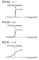
- Figures 9A to 9C are diagrams for showing the relationship between the square feature of the magnetization curve of a hard magnetic film 1 (or a magnetic film 1') and an MR curve of a magnetoresistance effect device of the invention.
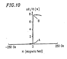
- Figure 10 is a graph showing an MR curve of a magnetoresistance effect device having a structure of [NiFeCo/Cu/CoPt/Cu] according to the invention.
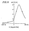
- Figure 11 is a graph showing an MR curve of an [NiFe/Cu/Co/Cu] artificial multilayer using magnetic films having different coercive forces of a prior art.
- Figure 12 is a graph showing an MR curve of an anti-ferromagnetic coupling type [NiFeCo/Cu/Co/Cu] artificial multilayer of a prior art.
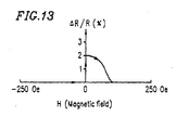
- Figure 13 is a graph showing an MR curve of an [NiFe/Cu/NiFe/FeMn] spin valve film using an anti-ferro-magnetic film of a prior art.
- Figure 14 is a graph showing an MR curve of a magnetoresistive changing portion of a memory device according to the invention.
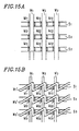
- Figures 15A and 15B are diagrams showing arrangement examples of conductor lines in a memory device according to the invention.
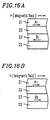
- Figures 16A and 16B are partial cross-sectional views showing the configurations and the spin alignment directions in the respective magnetic films of a magnetoresistance effect device according to the present invention.
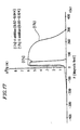
- Figure 17 is a graph showing an MR curve indicating the variation of the saturation magnetic field He in accordance with the addition of V in a magnetoresistance effect device according to the present invention.
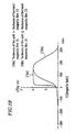
- Figure 18 is a graph showing the variation of an MR curve in accordance with the thickness of the magnetic films 21 and 23 in a magnetoresistance effect device according to the present invention.
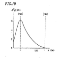
- Figure 19 is a graph showing the relationship between the magnetic field H end the resistance variation ratio ⁇ R/R in a magnetoresistance effect device according to the present invention.
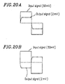
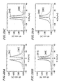
- Figures 20A and 20B are views showing the input/output characteristics of a memory device according to the present invention.
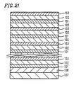
- Figure 21 is a sectional view of a magnetoresistance effect device according to the present invention.
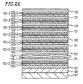
- Figure 22 is a sectional view of another magnetoresistance effect device according to the present invention.
- Figure 23 is a sectional view of still another magnetoresistance effect device according to the present invention.
- Figure 24 is a sectional view of still another magnetoresistance effect device according to the present invention.
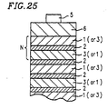
- Figure 25 is a structural view of a memory device/an amplifier including a multilayer device portion.
- Figure 26 is a graph showing the MR curves of an Si(100)/Cu(5)/NiFe(10)/Cu(2.4)/Ag(0.2)/Cu(2.4)/Co(10) device as a comparative example.
- Figures 27A and 27B are graphs showing the MR curves of a device A9 of the present invention and a glass/Cr(5)/[Co(3)/Cu(6)/NiFe(3)/Cu(6)] 10 device as a comparative example.
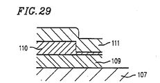
- Figure 29 shows a structure for a magnetic head according to the present invention.
- the present invention relates to a hard-film spin valve and a magnetoresistance effect device using multilayered hard-film spin valves .
- a hard-film spin valve and a magnetoresistance effect device using multilayered hard-film spin valves Unlike a conventional spin valve using an anti-ferromagnetic film of a conventional material such as Fe-Mn, in the hard-film spin valve of the invention, a unidirectionelly magnetized hard magnetic film performs similar functions to the anti-ferromagnetic film.
- FIG. 1A shows the construction of a magnetoresistance effect device of the invention.
- the magnetoresistance effect device includes a substrate 7 and a multilayer structure formed on the substrate 7 .
- the multilayer structure includes a hard magnetic film 1 , a non-magnetic metal film Z, and a soft magnetic film 3 .
- a device portion having such a multilayer structure is referred to as a magnetoresistive device portion.
- the magnetization curve of the hard magnetic film 1 has a good square feature, and hence the magnetization of the hard magnetic film 1 is not inverted in a weak magnetic field.
- the hard magnetic film 1 is formed so that the direction of the magnetization easy axis of the hard magnetic film 1 is substantially equal to the direction of the magnetic field to be detected.
- the "direction of the magnetic field to be detected" is typically identical with the direction of the signal magnetic field applied to the magnetoresistance effect device. However, in exceptional cases, the direction of the magnetic field to be detected may be different from the direction of the signal magnetic field to be applied to the magnetoresistance effect device. For example, the case where the direction of the signal magnetic field which is externally entered is bent by an L-shaped yoke is one of the exceptional cases.
- the non-magnetic metal film 2 is provided between the hard megnetic film 1 and the soft magnetic film 3 in order to reduce the force of the magnetic coupling between the hard magnetic film 1 and the soft magnetic film 3 .
- the magnetization of the soft magnetic film 3 can be easily inverted in a weak magnetic field.
- the soft magnetic film 3 is isolated from the magnetic coupling to the hard magnetic film 1 by the non-magnetic metal film 2 .
- a magnetic film having a coercive force of 20 Oe or more is referred to as "a hard magnetic film", and a magnetic film having a coercive force less than 20 Oe is referred to as "a soft magnetic film”.
- a hard magnetic film having a coercive force smaller than 100 Oe is referred to as "a semi-hard magnetic film”.
- the value of a coercive force used in thie specification is a value obtained by measuring with an AC of a relatively low frequency range (e.g., 60Hz).
- the hard magnetic film 1 is unidirectionally magnetized by using a ferromagnetic field
- a weak signal magnetic field having a direction opposite to the direction in which the hard magnetic film 1 is magnetized is applied to the magnetoresistance effect device
- the magnetization of the hard magnetic film 1 is not inverted, but the magnetization of the soft magnetic film 3 is inverted into the direction of the signal magnetic field.
- the magnetization direction of the hard magnetic film 1 is anti-parallel to the magnetization direction of the soft magnetic film 3.
- the magnetization direction of the hard magnetic film 1 is anti-parallel to that of the soft magnetic film 3
- the electrons in a current flowing through the magnetoresistance effect device is subjected to magnetic scattering at interfaces between the hard magnetic film 1 and the non-magnetic metal film 2 , and between the non-magnetic metal film 2 and the soft magnetic film 3.
- the resistance of the magnetoresistance effect element is increased.
- a weak signal magnetic field having the same direction as the direction in which the hard magnetic film 1 is magnetized is applied to the magnetoresistance effect device, the magnetization direction of the hard magnetic film 1 is parallel to that of the soft magnetic film 3 .
- the magnetoresistance effect device varies its electric resistance depending on the change of the signal magnetic field.
- FIG. 1B shows another construction of a magnetoresistance effect device according to the invention.
- the magnetoresistance effect device shown in Figure 1B includes a structure in which a structure of [the hard magnetic film 1 / the non-magnetic metal film 2 / and the soft magnetic film 3] shown in Figure 1A is stacked a plurality of times via the non-magnetic metal film 2.
- Such a stacked structure is represented by [the hard magnetic film 1 / the non-magnetic metal film 2 / the soft magnetic film 3 / the non-magnetic metal film 2] N (N indicates the number of repetitions).
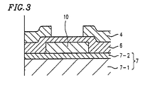
- FIG 3 shows the construction of a magneto-resistance effect type head according to the invention.
- a substrate 7 includes a ferrite 7-1 , or a Co-based amorphous film such as CoNbZr or the like formed on a nonmagnetic substrate or NiFe film 7-1 with high magnetic permeability formed on the substrate 7, and an insulating film 7-2 .
- a magnetoresistive device portion 10 is formed on the substrate 7.
- the magnetoresistive device portion 10 has the same structure as that of the multilayer of the magnetoresistance effect device shown in Figure 1A or 1B.
- An insulating film 6 is formed on the magnetoresistive device portion 10.
- a yoke 4 for guiding a signal magnetic flux from a magnetic medium to the soft magnetic film 3 is formed on the insulating film 6 .
- the yoke 4 is not necessarily required.
- the soft magnetic film 3 is formed so that the magnetization easy axis of the soft magnetic film 3 is orthogonal to the direction of the signal magnetic field applied to the magnetoresistance effect device.
- the magnetoresistive device portion 10 varies the electric resistance of the magnetoresistive device portion 10 depending on a weak signal magnetic field which is guided by the yoke 4 .
- a conductor line for a bias magnetic field for applying a bias to the above-mentioned magnetoresistive device portion having the multilayer structure can be provided in the vicinity of the magnetoresistive device portion.
- an anti-ferromagnetic film or a hard magnetic film may be attached to the end of the magnetoresistive device portion.
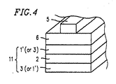
- FIG 4 shows the construction of a memory device according to the invention.
- the memory device includes a magnetoresistive change portion 11 and a conductor line 5 for allowing a current to flow.
- the conductor line 5 is disposed in the vicinity of the magnetoresistive change portion 11 so that the magnetic field produced by the current flowing through the conductor line 5 affecte the magnatoresistive change portion 11.
- the magnetoresistive change portion 11 is insulated from the conductor line 5 by the insulating film 6 .
- the magnetoresietive ohange portion 11 includes a magnetic film 1' , a non-magnetic metal film 2 , and a soft magnetic film 3 .
- the magnetization curve of the magnetic film 1' exhibits a good square feature, so that the magnetization of the magnetic film 1' is not inverted in a weak magnetic field.
- the non-magnetio metal film 2 is provided between the magnetic film 1' and the soft magnetic film 3 in order to reduce the magnetic coupling force between the magnetic film 1' and the soft magnetic film 3 .
- the magnetization of the soft magnetic film 3 can be easily inverted even in a weak magnetic field.
- the soft magnetic film 3 is isolated from the magnetic coupling to the magnetic film 1' by the non-magnetic metal film 2 .
- the magnetic film 1' has a coercive force which is larger than that of the soft magnetic film 3 . Moreover, the magnetic film 1' is required to have a coercive force smaller than the maximum magnetic field produced by the current flowing through the conductor line 5, so that the magnetization can be inverted by the magnetic field produced by the conductor line 5 .
- the purpose for the requirement is to represent the information to be stored in the memory device in accordance with the direction of the magnetization of the magnetic film 1'.
- the magnetoresistive change portion 11 can be constituted so as to include a structure in which the structure of [the magnetic film 1' / the non-magnetic metal film 2 / the soft magnetic film 3 ] shown in Figure 4 is stacked a plurality of times via the non-magnetic metal film 2 . In such a case, it is possible to obtain a memory device having a larger MR ratio.
- a current for storing information is caused to flow through the conductor line 5 .
- the magnetization of the magnetic film 1' and the magnetization of the magnetic film 3 are inverted.
- information is stored in accordance with the direction of the magnetization of the magnetic film 1' .
- the information to be stored is "1".
- the information to be stored is "0".
- a weak current for reading-out information is used.
- a weak magnetic field having a direction opposite to that of the magnetization of the magnetic film 1' is applied to the magnetoresistive change portion 11 by the weak current for reading-out information, the magnetization of the magnetic film 1' is not inverted, but the megnetization of the soft magnetic film 3 is inverted into the direction of the weak magnetic field.
- the direction of the magnetization of the magnetic film 1' is anti-parallel to that of the magnatization of the soft magnetic film 3 , so that the resistance of the magnetoresistive change portion 11 is increased.
- a weak current for reading-out information is first caused to flow through the conductor line 5 in a certain direction (initialization by weak current), and then a weak current for reading-out information is caused to flow through the conductor line 5 in a direction opposite to the certain direction (reversal of weak current).
- Figure 6B shows the case where a weak current is caused to flow through the conductor line 5 in a direction perpendicular to the drawing sheet from the back face to the front face thereof (initialization by weak current)
- Figure 6C shows the case where a weak current is caused to flow through the conductor line 5 in a direction perpendicular to the drawing sheet from the front face to the back face thereof (reversal of weak current).
- the information stored in the magnetic film 1' is detected as the change of the resistance of the magnetoresistive change portion 11 .
- the resistance of the magnetoresistive change portion 11 during the reversal of weak current is increased as compared with the case of the initialization by weak current.
- the resistance of the magnetoresistive change portion 11 during the reversal of weak current is decreased as compared with the case of the initialization by weak current (see Figure 6D ). In this way, the information store in the magnetic film 1' can be read-out in a nondestructive manner.
- the weak current may be a pulse-type weak current.
- Figure 5 shows another construction of a memory device according to the invention.
- the memory device shown in Figure 5 has a structure in which a structure of [the magnetic film 1' / the non-magnetic metal film 2 / the soft magnetic film 3] shown in Figure 4 is stacked a plurality of times via the non-magnetic metal film 2 .
- the coercive forces of the plurality of magnetic films 1' included in the stacked structure are different from each other. If the number of magnetic films 1' in which the magnetization thereof is not inverted by a predetermined signal magnetic field is related to a desired value, multivalue information can be stored in the plurality of magnetic films 1'. In this way, it is possible to obtain a memory device capable of storing multivalue information.
- such a memory device operates as shown in Figures 7A to 7C.
- an amplifying device is the same as that of the above-described memory device according to the invention except for the coercive forces of the magnetic films 1'. Therefore, the detailed description thereof is omitted.
- the amplifying device is initialized (see Figure 8A ). That is, a strong current pulse is caused to flow through the conductor line 5 , the magnetization of the magnetic film 1' is fixed in one direction.
- the amplifying device is constituted so that the magnetization easy axis of the magnetic film 1' substantially agrees with the direction of the magnetic field produced by the strong current pulse.
- the memory device according to the invention is different from the magnetoresistance effect type head according to the invention in that the magnetic film 1' is not necessarily required to be a hard magnetic film with a large coercive force in the memory device of the invention.
- the magnetic Film 1' is a semi-hard magnetic film, as far as the magnetic film has a coercive force larger than that of the soft magnetic film 3 .
- the reason is that, when information is written into the memory device, it is necessary to invert the magnetization of the magnetic film 1' .
- the magnetic film 1' is a hard magnetic film.
- it is desired that the magnetic film 1' is a semi-hard magnetic film.
- the magnetic film 1' is a hard magnetic film, because the magnetization of the magnetic film 1' is required not to be inverted by the signal magnetic field.
- the magnetic film 1' is not necessarily a hard magnetic film, as far as the magnetic film 1' is a magnetic film having a magnetization curve with a good square feature. The reason is that the signal current flowing through the conductor line 5 during the amplifying operation is small, and hence the magnetic field produced by the signal current is also small.
- a magnetic film 3' may be inserted at, at least one of the interface between the magnetic film 1 (or the magnetic film 1' ) and the non-magnetic metal film 2 , and the interface between the soft magnetic film 3 and the non-magnetic film 2 .
- the magnetic film 3' is a magnetic film including Co as a main component. It is preferred that the magnetic film 3' has a thickness of 0.1 to 1 nm. In the case where the thickness of the magnetic film 3' is 0.1 nm or less, the effect for improving the MR ratio is small.
- a magnetic film 3' is attached to have a thickness of 1 nm or more at the interface with the soft magnetic film 3 , because the deteriorate the soft magnetic property of the soft magnetic film 3 .
- a magnetic film 3' may be inserted between the hard magnetic film 1 (or the magnetic film 1' ) and the non-magnetic metal film 2 .
- the magnetic film 3' is provided on both faces or on one face of the hard magnetic film 1 (or the magnetic film 1' ).
- the thickness of the magnetic film 3' is set in the range of 0.1 to 2 nm.
- the composition of the magnetic film 3' includes at least one element selected from Co, Ni, Fe as the main component. If the thickness of the magnetic film 3' is smaller than 0.1 nm, the effect for improving the MR ratio is small.
- the thickness of the magnetic film 3' is 2 nm or more, the square feature of the magnetization curve and the coercive force of the hard magnetic film 1 (or the magnetic film 1' ) may be easily degraded.
- the thickness of the magnetic film 3' is 1 nm or less. This is because that the magnetization curve of the magnetic film 1 exhibits a good square feature, and the magnetic film 1 is required to be a hard magnetic film having a relatively large coercive force.
- Figure 2A shows an example in which, in the sandwich-type magnetoresistance effect device shown in Figure 1A, the magnetic film 3' is inserted at the interface between the hard magnetic film 1 (or the magnetic film 1' ) and the non-magnetic metal film 2 .
- Figure 2B shows an example in which, in the stacked-type magnetoresistance effect device shown in Figure 1B, the magnetic film 3' is inserted at the interface between the hard magnetic film 1 (or the magnetic film 1' ) and the non-magnetic metal film 2 .
- the magnetic film 3' is provided on both faces of the hard magnetic film 1 (or the magnetic film 1' ). It is also appreciated that the magnetic film 3' may be provided on only one face of the hard magnetic film 1 (or the magnetic film 1' ).
- the magnetoresistance effect device shown in Figure 2B shows a larger MR ratio, as compared with the magnetoresistance effect device shown in Figure 2A.
- the respective thicknesses of the hard magnetic film 1 (or the magnetic film 1' ), the non-magnetic metal film 2 , the soft magnetic film 3 , and the magnetic film 3' are not so large, considering the mean free path of electrons.
- the MR ratio is increased as the stacked number of components is incressed. When the components are stacked three times or more, the effect is remarkably observed. When the components are stacked ten times or more, the effect is substantially saturated.
- the stacked number of films is desired to be five times or less, except for the cases where a current is caused to flow in a direction perpendicular to the film face during the operation.
- the magnetization curve of the hard magnetic film 1 (or the magnetic film 1' ) has a good square feature.
- Figures 9A to 9C show the relationships between the square ratio S of the hard magnetic film 1 (or the magnetic film 1' ) and the MR curve of the magnetoresistance effect device according to the invention.
- the square ratio S when the square ratio S is smaller than 0.7, the MR curve in the vicinity of the zero magnetic field is deteriorated.
- the deterioration of the MR curve in the vicinity of the zero magnetic field may deteriorate the reproduction sensitivity and the linearity of the magnetoresistive type head and the amplifying device, and also a memory device may erroneously operate during the recording and reproduction due to the erroneous operation of magnetization inversion of the magnetic film 1'.
- it is important that the hard magnetic film 1 (or the magnetic film 1' ) is unidirectionally magnetized, and hence the magnetic film has such a character that the magnetized state is kept and the magnetization is not inverted in a weak magnetic field.
- the magnetization of the magnetic film 1 is fixed in one direction. Accordingly, the magnetic film 1 is required to be a hard magnetic film having a large coercive force, and it is desired that the coercive force in the bulk state or in the thick film state of a film of the same composition is 500 Oe or more. In addition, it is desired that the magnetic film 1 has a good corrosion resistance.
- the material for the magnetic film 1 include Co 0.75 Pt 0.25 , Co 0.84 Ta 0.02 Cr 0.14 , Co 0.70 Pt 0.10 Cr 0.12 , Co 0.5 Fe 0.5 , and the like. At present, in view of the coercive force and the corrosion resistance, CoPt is the most suitable material.
- CoFe is the most suitable material.
- the Curie temperatures of these films are sufficiently higher than the Néel temperature of the Fe-Mn film which is used in the conventional spin valve. Thus, the dependence of the characteristics of these films on temperature can advantageously be reduced.
- the magnetic film 1' may alternatively be a semi-hard magnetic film of Co 0.5 Fe 0.5 , Co, or the like.
- the coercive force of the magnetic film 1' can be adjusted by changing the film thickness.
- the magnetic film 1' may be a semi-hard magnetic film of or the like having a thickness of 3 nm or less.
- the magnetization of the magnetic film 1' is fixed in one direction. Accordingly, it is desired that the magnetic film 1' is made of a hard magnetic material having a large coercive force. However, in practical use, the magnetic film 1' may be made of a semi-hard magnetic material. This is because the signal current which flows through the conductor line 5 is very small, so that the magnetic field produced by the signal current is also very small.
- the magnetic film 3 is required to have a soft magnetic property in which the magnetization can easily be inverted by a small magnetic field so that the magnetoresistance can easily be changed. Also, it is preferred that the soft magnetic film 3 is a film with low magnetostriction. This is because, if a film has high magnetostriction in practical use, it may often cause a noise, and there occurs a variation in characteristics among the fabricated devices.
- Representative examples of such a material include Ni 0.8 Fe 0.15 Co 0.05 , Ni 0.8 Fe 0.1 Co 0.1 , Ni 0.68 Co 0.2 Fe 0.12 and the like.
- Such a film include Co 0.44 Fe 0.3 Ni 0.26 , Co 0.6 Fe 0.2 Ni 0.2 , Co 0.7 Fe 0.2 Ni 0.1 and the like.
- the low magnetostriction which is required for the magnetoresistance effect device such as a sensor or an MR head can be attained (i.e., the magnetostriction is at about 1 ⁇ 10 -8 or less).
- the soft magnetic film 3 may be a film of the Co-based amorphous alloy Co 0.75 Fe 0.05 B 0.2 .
- the Co-based amorphous alloy film has such a disadvantage that the specific resistance is somewhat higher as compared with the above-described materials for the soft magnetic film, but has such advantages that the magnetization can be inverted in a very weak magnetic field, and that the film has a high magnetic permeability substantially at a zero magnetostriction.
- the non-magnetic metal film 2 is desired to be less reactive and to be difficult to form a solid solution at the interface with the hard magnetic film 1 (or the magnetic film 1' ) and at the interface with the soft magnetic film 3 . Also, the non-magnetic metal film 2 is required to be a film which can form a flat and clear interface with the magnetic film. In addition, the non-magnetic metal film 2 is required to be non-magnetic, in order to cut the magnetic coupling between the hard magnetic film 1 (or the magnetic film 1' ) and the soft magnetic film 3 .
- Cu, Ag, Au or the like is suitable for the non-magnetic metal film 2 . In view of the MR characteristic, Cu is the moat suitable material.
- the thickness of the non-magnetic metal film 2 is 10 nm or more, the MR ratio of the whole device is reduced. Accordingly, the thickness of the non-magnetic metal film 2 is set to be less than 5 nm. On the other hand, if the thickness of the non-magnetic metal film 2 becomes smaller than 1 nm, the hard magnetic film 1 (or the hard magnetic film 1' ) is magnetically coupled with the soft magnetic film 3 , and hence a large magnetoresistance effect cannot be attained.
- a magnetic film 3' which is inserted between the hard magnetic film 1 (or the magnetic film 1' ) and the non-magnetic metal film 2 , or between the soft magnetic film 3 and the non-magnetic metal film 2 can increase the magnetoresistance effect.
- the magnetic film 3' includes Co or at least one element selected from Ni, Co, and Fe as the main component.
- the magnetic film 3' may be made of Co. Co 0.7 Fe 0.1 or Co 0.44 Fe 0.3 Ni 0.26 , Co 0.7 Fe 0.2 Ni 0.1 or the like for the above-mentioned soft magnetic film 3 .
- the yoke 4 of the magnetic head shown in Figure 3 is desired to be soft magnetic and to have high magnetic transmittance.
- a Co-based amorphous magnetic alloy film is suitably used. As an example thereof, is used.
- the conductor line 5 of the memory device (or the amplifying device) shown in Figure 4 is a low-resistive metal-film line for generating a magnetic field.
- conductor lines may not intersect each other as shown in Figure 15A or conductor lines may interaect each other on respective devices as shown in Figure 15B.
- W 1 to W 3 indicate conductor lines (word lines)
- S 1 to S 3 indicate sense lines.
- the sense lines S 1 to S 3 are formed by the magnetoresistive change portions M ij (shaded portions in the figure) and shunting conductor portions (white portions in the figure).
- a current is allowed to flow through the word line W 1 and the sense line S 1 .
- information is stored in the magnetoresistive change portion M 11 by a synthetic magnetic field produced by the current flowing through the word line W 1 and the sense line S 1 .
- a pulse current is allowed to flow through the word line W 1 .
- the information stored in the magnetoresistive change portion M 11 can be read out.
- W 1 to W 2 and W' 1 and W' 2 indicate conductor lines (word lines)
- S 1 and S 2 indicate sense lines.
- the sense lines S 1 and S 2 are formed by the magnetoresistive change portions M ij (shaded portions in the figure) and shunting conductor portions (white portions in the figure). For example, when information is to be stored into a magnetoresistive change portion M 11 , a current is allowed to flow through the word line W 1 and the word line W' 1 .
- the sandwich-type magnetoresistive device as shown in Figure 1A and the stacked-type magnetoresistive device as shown in Figure 1B were fabricated on a substrate by a multi-target sputtering apparatus.
- the sandwich-type magnetoresistive device had the following structure: A : the substrate / CoNiFe (15) / Cu (2.2) / CoPt (10) (parenthesized values indicate the thicknesses (nm)), and the stacked-type magnetoresistive device had the following structure: A' : the substrate / [CoNiFe (3) / Cu (2.2) / CoPt (5) / Cu (2.2)] 5 .
- the respective film thicknesses were controlled by using a shutter, and CcPt of the hard magnetic film 1 was magnetized. Then, the MR characteristics of the obtained devices were measured at room temperature in the applied magnetic field of 100 oe.
- the MR ratios for the devices having the structures A and A' were 4% and 6%, respectively.
- the widths of the magnetic field in which the MR was varied were 3 Oe and 5 Oe, respectively. From this figure, the following facts are found. As compared with the case where a magnetic film having different coercive forces is used as shown in Figure 11, the device of the invention can operate in a very weak magnetic field and the linearity property is improved. As compared with the anti-ferromagnetic coupling type shown in Figure 12, the operating magnetic field of the device of the invention is small. As compared with the spin valve using the anti-ferromagnetic film shown in Figure 13, the device of the invention has an improved MR ratio.
- Example 2 In the same way as that in Example 1, by using Co 0.75 Pt 0.25 (the hard magnetic film 1), Co 0.7 Ni 0.1 Fe 0.2 (the soft magnetic film 3), and Cu (the non-magnetic metal film 2) as targets, the hard magnetic film 1, the non-magnetic metal film 2, the soft magnetic film 3, and the non-magnetic metal film 2 were sequentially deposited.
- B the substrate / [NiCoFe (6) / Cu (2.2) / CoPt (5) / Cu (2.2)] 20 .
- the material of CoPt of the hard magnetic film 1 was magnetized, and than the hard magnetic film 1 was made to have a columnar shape of 25 ⁇ m ⁇ 25 ⁇ m by using a lithography technique. Thereafter, the MR characteristics of the device were measured by a 4-terminal mathod using lithography. The MR ratio was 18% in the applied magnetic field of 100 Oe, and the width of the magnetic field in which the MR was varied was 20 Oe.
- the hard magnetic film 1, the non-magnetic metal film 2, and the soft magnetic film 3 were sequentially deposited by a multi-target sputtering apparatus by using (the hard magnetic film 1), Cu (the non-magnetic metal film 2 ), and Ni 0.68 Co 0.2 Fe 0.12 (the soft magnetic film 3 ) as targets.
- the material of CoPt of the hard magnetic film 1 was magnetized.
- An insulating film 6 and CoNbZr were deposited thereon by using SiO 2 (the insulating film 6) and Co 0.02 Nb 0.12 Zr 0.06 (the yoke 4 ) as targets.
- MR heads megnetoresistance effect type heads as shown in Figure 3 having the following structures were fabricated: C : the substrate / CoPt (15) / Cu (2.2) / NiCoFe (15) / SiO 2 (100) / CoNbZr (1000), and C' : the substrate / [CoPt (5) / Cu (2.2) / NiCoFe (4) / Cu (2.2) ] 3 / SiO 2 (100) / CoNbZr (1000).
- an MR head having a conventional structure in which the conventional materials of Ni 0.8 Fe 0.2 and Co 0.62 Nb 0.12 Zr 0.06 were respectively used for the magnetoresistance effect film and the yoke was fabricated.
- An alternating current signal magnetic field of 100 Oe was applied to both of the conventional MR head end the MR heads of the invention, so as to compare the reproduction outputs of the respective heads. It was found that the MR heads having the structures C and C' of the invention could attain the outputs which were respectively about 1.5 times and 3 times as large as those of the conventional MR head as the comparative example.
- a current was allowed to flow through the conductor line 5 as shown in Figure 6A , so as to unidirectionally magnetize the magnetic film 1'.
- a weak current was allowed to flow through the conductor line 5 , so as to align the magnetization of the soft magnetic film 3 in one direction.
- the weak current flowing through the conductor line 5 was reversed, and the change of resistance in the magnetoresistive change portion was measured at this time. It was confirmed that the change of resistance was definitely changed to be plus (increase) or minus (decrease) depending on the magnetized direction recorded in the magnetic film 1', as shown in Figure 6D.
- the sandwich-type magnetoresistive device hod the following structure: F : the substrate / NiCoFe (10) / Co (0.2) / Cu (2) / Co (0.2) / CoPt (3) (parenthesized values indicate the thicknesses (nm)), and the stacked-type magnetoresistive device had the following structure: F' : the substrate / [NiCoFe (3) / Co (0.2) / Cu (2) / Co (0.2) / Copt (3) / Co (0.2) / Cu (2)] N / NiCoFe (3), where N indicates the stacked number of films and N is 5 in this example.
- the respective film thicknesses were controlled by using a shutter, and Copt of the hard magnetic film 1 was magnetized.
- the MR characteristics of the obtained devices were measured at room temperature in the applied magnetic field of 100 Oe.
- the MR ratios for the devices having the structures F and F' were 6% and 8%, respectively.
- the widths of the magnetic field in which the MR was varied were 3 Oe and 5 Oe, respectively.
- Figure 10 shows an exemplary MR curve of the stacked-type device.
- the sandwich-type magnetoresistive device as shown in Figure 2A and the stacked-type magnetoresistive device as shown in Figure 2B wore fabricated on a substrate by a multi-target sputtering apparatus.
- the sandwich-type magnetoresistive device had the following structure: G : the substrate / NiCoFe (15) / Cu (2.3) / CoNiFe (0.5) / CoPt (10) (parenthesized values indicate the thicknesses (nm)), and the stacked-type magnetoresistive device had the following structure: G' : the substrate / [NiCoFe (7) / Cu (2.2) / CoNiFe (0.5) / CoPt (4) / CoNiFe (0.5) / Cu (2.2)] N , where N indicates the stacked number of films and N is 5 in this example.
- the respective film thicknesses were controlled by using a shutter, and CoPt of the hard magnetic film 1 was magnetized.
- the MR characteristics of the obtained devices were measured at room temperature in the applied magnetic field of 100 Oe.
- the MR ratios for the devices having the structures G and G' were 6% and 9%, respectively.
- the widths of the magnetic field in which the MR was varied were 3 Oe and 5 Oe, respectively.
- devices in which Co 0.7 Fe 0.2 Ni 0.1 (the magnetic film 3') was not inserted at the interface were fabricated.
- the MR ratios of the comparative examples were 4% and 6% which were lower than those of the devices of the invention.
- a magnetoresistive device portion having the following structure was fabricated by a multi-target sputtering apparatus by using Co 0.75 Pt 0.25 (the hard magnetic film 1), Cu (the non-magnetic metal film 2 ), Ni 0.68 Co 0.2 Fe 0.12 (the soft magnetic film 3 ), and Co (the magnetic film 3' ) as targets: H : [NiCoFe (7) / Cu (2.1) / Co (0.4) / CoPt (4) / Co (0.4) / Cu (2.1)] 3 .
- the material of CoPt of the hard magnetic film 1 was magnetized.
- An insulating film 6 and CoNbZr were deposited thereon by using SiO 2 (the insulating film 6) and Co 0.82 Nb 0.12 Zr 0.06 as targets.
- the deposited films were patterned by lithography, so as to produce the yoke portion 4.
- a magnetoresistance effect type head as shown in Figure 3 having the following structure was fabricated: I : the substrate / [NiCoFe (7) / Cu (2.1) / Co (0.4) / CoPt (4) / Co (0.4) / Cu (2.1)] 3 / SiO 2 (100) / CoNbZr (1000).
- an MR head having a conventional structure in which the conventional materials of Ni 0.8 Fe 0.2 and Co 0.82 Nb 0.12 Zr 0.06 were respectively used for the magnetoresistance effect film end the yoke was fabricated.
- An alternating current signal magnetic field of 100 Oe was applied to both the conventional MR head and the MR head of the invention, so as to compare the reproduction outputs of the respective heads. It was found that the MR head having the structure I of the invention could attain an output which was about 4 times as large as that of the conventional MR head as the comparative example.
- the reference numeral 1' in Figures 6A to 6C denotes a film including the magnetic film 1' and the magnetic film 3'.
- the megnetoresistive change portion was fabricated so as to have the following stacked structure: A memory device was fabricated by using the magnetoresistive change portion having the stecked structure. In the same way as described above, the operation of the memory device was checked. It was confirmed that, during the information read-out, the output voltage of the memory device having the structure J' was about twice as high as that of the memory device having the structure J.
- One type of memory device was provided in such a manner that a current was allowed to flow through the conductor line 5 as shown in Figure 7A , and the magnetization of the three kinds of magnetic films 1, 1' , and 1" (NiFe) and the magnetization of the soft magnetic film 3 was inverted, so as to record information.
- the other type of memory device was provided in such a manner that a magnetic field which is smaller than the coercive force of the magnetic films 1 end 1' (CoPt, CoCrTa) but larger than the coercive force of the magnetic film 1" was produced, and hence the magnetization of the magnetic film 1" and the magnetization of the soft magnetic film 3 (NiCoFe) was inverted, so as to record information.
- a weak current pulse was allowed to flow through the conductor line 5 , so that only the magnetization of the soft magnetic film 3 was inverted, and the change of resistance of the magnetoresistive change portion at this time was messured.
- a soft magnetic film 21 with a thickness of 1 to 20 nm, a hard magnetic film 23 with a thickness of 1 to 20 nm, having respectively different coercive forces, are alternately stacked, and non-magnetic metal films 22 with a thickness of 1 to less than 5 nm are interposed between the soft magnetic films 21 and the hard magnetic film 23 to be alternately stacked.
- the main component of the soft magnetic film 21 is expressed by the following formula: Ni X Co Y Fe Z
- the hard magnetic film 23 is composed of a CoFe based material having a relatively large resistance variation ratio ⁇ R/R, and the main component thereof is expressed by the following formula: Co Y Fe 1-Y where Y is expressed by an atomic composition ratio: 0.3 ⁇ Y ⁇ 0.7
- the CoFe based material to which V is added has a very satisfactory square ratio of 0.9 or more, and the component thereof is expressed by the following formula: (Co Z Fe 1-Z ) Z' V 1-Z . where Z and Z' are expressed by the atomic composition ratios as follows: 0.3 ⁇ Z ⁇ 0.7 0.9 ⁇ Z' ⁇ 0.98
- the saturation magnetic field strength Hs of the MR curve is reduced in the case where the amount to be added is small, i.e., in the range of 0.02 to 0.04 %, so that the characteristics, optimized for using this device as a memory device, may be obtained.
- the saturation magnetic field strength Hs of the MR curve is increased, so that the characteristics optimal for a magnetoresistance effect device and a magnetoresistance effect type head are exhibited.
- the non-magnetic metal film 22 is preferably composed of a material showing little reaction with a Ni-Co-Fe based magnetic material in the interface therebetween, and therefore any of Cu, Ag and Au is suitably used.
- the soft magnetic film 21 is composed of a soft magnetic material exhibiting a small magnetostriction, a small coercive force, and a satisfactory square feature
- the hard magnetic film is composed of a semi-hard or a hard magnetic material exhibiting a relatively large coercive force and a satisfactory square feature.
- the soft magnetic film 21 is not necessarily a ternary film such as that described above, but may be a binary magnetic film having soft magnetism and a relatively large resistance variation ratio ⁇ R/R, e.g., a Ni-Co based binary magnetic film.
- the main component of the soft magnetic film 21 is expressed by the following formula. Ni X Co 1-X where X is expressed by an atomic composition ratio as follows: 0.05 ⁇ X ⁇ 0.4
- the soft magnetic films 21 and the hard magnetic films 23 are alternately stacked with non-magnetic metal films 22 interposed therebetween, if the thickness of the soft magnetic film 21 is set to be larger than that of the hard magnetic film 23 , then a large resistance variation ratio may be obtained in very small magnetic fields, as shown in Figure 18 .
- the spins in the hard magnetic film 23 are also reversed as indicated by the arrow B 2 .
- the spin alignment direction in the soft magnetic film 21 becomes parallel to the spin alignment direction in the hard magnetic film 23; the spin scattering of the conductive electrons becomes small; and the electrical resistance values are reduced.
- Figure 19 shows the values of the resistance variation ratio ⁇ R/R in the above-described magnetoresistance effect device in association with the variation of the applied magnetic field H.
- the position 19a corresponds to the state shown in Figure 16A; while the position 19b corresponds to the state shown in Figure 16B .
- Figure 19 is a graph showing the relationship between the strength of the magnetic field H and the resistance variation ratio ⁇ R/R thus obtained.
- the soft magnetic film 21 it is preferable for the soft magnetic film 21 to have a small magnetostriction. This is because a noise is likely to occur if a magnetic film having a large magnetostriction is employed for an MR head.
- composition ratio of a Ni-rich Ni-Co-Fe based alloy expressed by the above-described formula (3) satisfies the expression (4), then the magnetostriction of such an alloy becomes small, so that the alloy exhibits soft magnetism.
- a typical composition ratio of such an alloy is or the like.
- the wear resistance and the corrosion resistance, Nb, Mo, Cr, W, Ru and the like may be added to the composition represented by the expression (4).
- the CoFe based alloy expressed by the formula (5) exhibits a satisfactory square feature and semi-hard or hard magnetism when the CoFe alloy satisfies the expression (6).
- the CoFe based alloy expressed by the formula (7) to which V is added so as to satisfy the expression (8) may arbitrarily vary the coercive force thereof depending on the added amount of V and may improve the square feature thereof.
- the magnetic films 21 and the hard magnetic film 23 having respectively different coercive forces may be obtained.
- the thickness of the soft magnetic film 21 and the hard magnetic film 23 is smaller than 1 nm, the decrease in the strength of the magnetic field owing to the reduction of Curie temperature and the like are disadvantageously caused at room temperature.
- the thickness of the respective magnetic films 21 and 23 is required to be set at smaller than 20 nm in order to utilize the effects of the stacking structure to be obtained according to the present invention.
- the film thickness of the soft magnetic film 21 exhibiting soft magnetic characteristics is set to be larger than that of the hard magnetic film 23 exhibiting semi-hard magnetic characteristics or hard magnetic characteristics, the soft magnetic characteristics are improved and the rising of the characteristics in a very weak magnetic field becomes abrupt.
- the thickness of these magnetic films 21 and 23 is preferably set in the range of 1 to 20 nm.
- the non-magnetic metal film 22 interposed between these magnetic films 21 and 23 is required to be less reactive with a Ni-Fe-Co based magnetic film in the interface therebetween, end is also required to be non-magnetic. Therefore, Cu, Ag, Au and the like are suitable as a material for the non-magnetic metal film 22. If the thickness of this non-magnetic metal film 22 is smaller than 1 nm, then it becomes difficult to realize the state as shown in Figure 16A, where the soft magnetic film 21 and the hard magnetic film 23 are magnetically coupled, and the spin alignment directions in the soft magnetic film 21 and the hard magnetic film 23 having respectively different coercive forces become antiparallel to each other.
- the thickness of the non-magnetic metal film 22 is preferably set in the range of 1 to 10 nm.
- Magnetoresistive devices having the following configurations (Samples Nos. A2, B2, and C2) are formed on a glass substrate by using a sputterer.
- Samples A2 and B2 are comparative examples not falling within the scope of the claims.
- composition ratios of Ni-Fe, Ni-Co, Ni-Co-Fe and Co-Fe are set to be Ni 0.8 Fe 0.2 , Ni 0.8 Co 0.2 , Ni 0.8 Co 0.1 Fe 0.1 and Co 0.5 Fe 0.5 , respectively.
- the film thickness is controlled by power and shutter speed.
- magnetoresistive devices having the following configurations (Samples Nos. D2, E2, and F2) are formed on a glass substrate.
- the film is sputtered in the magnetic field so that the easy axis of the magnetic film exhibiting soft magnetism crosses the easy exis of the magnetic film exhibiting semi-hard magnetism at a right angle.
- the magnetoresistance effect of the film is measured by applying a magnetic field in a direction of the magnetization hard axis of the magnetic film exhibiting soft magnetism.
- the switching field Ht of the film shown in Table 1 are the values in the direction of the magnetization hard axis.
- the magnetoresistance effect device of this example exhibits practical characteristics, that is to say, the device shows a large resistance variation ratio ⁇ R/R at room temperature and a relatively small switching field Ht in the rising portion.
- magnetoresistive devices having the following configurations (Samples Nos. A3, B3, and C3) are formed on a glass substrate by using a sputterer.
- Samples A3 and B3 are comparative examples not falling within the scope of the claims.
- composition ratios of Ni-Fe, Ni-Co, Ni-Co-Fe and Co-Fe-V are set to be Ni 0.8 Fe 0.2 , Ni 0.5 Co 0.2 , Ni 0.8 Co 0.1 Fe 0.1 and Co 0.5 Fe 0.46 V 0.04 , respectively.
- the film thickness is controlled by power and shutter speed.
- magnetoresistive devices having the following configurations (Samples Nos, D3, E3, and F3) are formed on a glass substrate.
- the film is sputtered in the magnetic field so that the easy axis of the magnetic film exhibiting soft magnetism crosses the easy axis of the magnetic film exhibiting semi-hard magnetism at a right angle.
- the magnetoresistance effect of the film is measured by applying a magnetic field in a direction of the magnetization hard axis of the magnetic film exhibiting soft magnetism.
- the switching field Ht of the film shown in Table 2 are the values in the direction of the magnetization hard axis.
- the magnetoresistance effect device of this example exhibits practical characteristics, that is to say, the device shows a large resistance variation ratio ⁇ R/R at room temperature and a relatively small switching field Ht in the rising portion.
- magnetoresistive devices having the following configurations (Samples Nos. A4, B4, and C4) are formed on a glass substrate by using a sputterer.
- Samples A4 and B4 are comparative examples not falling within the scope of the claims.
- composition ratios of Ni-Fe, Ni-Co, Ni-Co-Fe and Co-Fe-V are set to be Ni 0.8 Co 0.1 Fe 0.1 and Co 0.52 Fe 0.39 V 0.09 , respectively.
- the film thickness is controlled by Dower and shutter speed.
- magnetoresistive devices having the following configurations (Samples Nos. D4, E4, and F4) are formed on a glass substrate.
- the film is sputtered in the magnetic field so that the easy axis of the magnetic film exhibiting soft magnetism crosses the easy axis of the magnetic film exhibiting semi-hard magnetism at a right angle.
- the magnetoresistance effect of the film is measured by applying a magnetic field in a direction of the magnetization hard axis of the magnetic film exhibiting soft magnetism.
- the switching field Ht of the film shown in Table 3 are the values in the direction of the magnetization hard axis, while the saturation magnetic fields Hs are the values in the direction of the magnetization easy axis.
- the magnetoresistance effect device of this example exhibits practical characteristics usable for a magnetoresistance effect device and a magnetoresistance effect type head, that is to say, the device shows a large resistance variation ratio ⁇ R/R at room temperature, a relatively small switching field Ht in the rising portion, and a large saturation magnetic field Hs.
- magnetoresistive devices having the following configurations (Samples Nos. A5, B5, and C5) are formed on a glass substrate by using a sputterer.
- composition ratios of Ni-Fe, Co-Fe, Ni-Co-Fe and Co-Fe-V are set to be Ni 0.5 Fe 0.5 , Co 0.5 Fe 0.5 , Ni 0.8 Co 0.1 Fe 0.1 , and Co 0.49 Fe 0.49 V 0.02 , respectively.
- the film thickness is controlled by power and shutter speed.
- magnetoresistive devices having the following configurations (Samples Nos. D5, E5, and F5) are formed on a glass substrate.
- the film is sputtered in the magnetic field so that the easy axis of the magnetic film exhibiting soft magnetism crosses the easy axis of the magnetic film exhibiting semi-hard magnetism at a right angle,
- the magnetoresistance effect of the film is measured by applying a magnetic field in a direction of the magnetization hard axis of the magnetic film exhibiting soft magnetism.
- the switching field Ht of the film shown in Table 4 are the values in the direction of the magnetization hard axis.
- the magnetoresistance effect device of this example exhibits practical characteristics useful for a high-sensitivity magnetoresistance effect device, a magnetoresistance effect type head and memory device, that is to say, the device shows more abrupt characteristics and a smaller switching field Ht in the rising portion by setting the thickness of the soft magnetic film thicker than that of the semi-hard magnetic film.
- magnetoresistive devices having the following configurations (Samples Nos. A6, B6, and C6) are formed on a glass substrate by using a sputterer.
- Samples A6 and B6 are comparative examples not falling within the scope of the claims.
- composition ratios of Ni-Fe, Ni-Co, Ni-Co-Fe and CO-Fe-V are set to be Ni 0.8 Fe 0.2 , Ni 0.8 Co 0.2 , Ni 0.8 Co 0.1 Fe 0.1 and Co 0.49 Fe 0.49 V 0.02 , respectively.
- the film thickness is controlled by power and shutter speed.
- magnetoresistive devices having the following configurations (Samples Nos. D6, E6, and F6) are formed on a glass substrate.
- the film is sputtered in the magnetic field so that the easy axis of the magnetic film exhibiting soft magnetism crosses the easy axis of the magnetic film exhibiting semi-hard magnetism at a right angle.
- the magnetoresistance effect of the film is measured by applying a magnetic field in a direction of the magnetization hard exis of the magnetic film exhibiting soft magnetism.
- the switching field Ht of the film shown in Table 5 are the values in the direction of the magnetization hard axis, while the saturation magnetic fields Hs are the values in the direction of the magnetization easy axis.
- the magneto-resistance effect device of this example exhibits practical characteristics useful for a memory device, that is to say, the device shows a large resistance variation ratio ⁇ R/R at room temperature, a relatively small switching field Ht in the rising portion, and a small saturation magnetic field Hs.
- an MR head is produced using the magnetoresistive devices.
- the following magnetoresistance effect films are used for forming the head.
- composition ratios of Ni-Fe, Co-Fe, Co-Fe-V, and Ni-Co-Fe are set to be Ni 0.5 Fe 0.5 , Co 0.5 Fe 0.5 , Co 0.52 Fe 0.39 V 0.09 and Ni 0.7 Co 0.2 Fe 0.1 , respectively.
- the film is sputtered in the magnetic field so that the easy axis of the magnetic film exhibiting soft magnetism crosses the easy axis of the magnetic film exhibiting semi-hard magnetism at a right angle.
- the stacking cycles are set to be 3.
- the resistance variation ratios ⁇ R/R shown in Table 6 are those measured before forming a head.
- the output ratios shown in Table 6 are obtained by comparing the output of the MR head of this example with that of a conventional MR head. As is apparent from the results shown in Table 6, according to the MR head of this example, a larger output may be obtained than from a conventional MR head.
- a memory device shown in Figure 4 was produced by a photolithography technique using the magnetoresistive devices.
- the following magnetoresistance effect films were used for forming the memory device.
- composition ratios of Ni-Fe, Co-Fe, Co-Fe-V and Ni-Co-Fe are set to be Co 0.5 Fe 0.5 , Co 0.49 Fe 0.49 V 0.02 and Ni 0.7 Co 0.2 Fe 0.1 , respectively.
- the measurement is performed in the following manner. First, an electric current of +100 mA is supplied through conductor lines 5, thereby magnetizing the semi-hard magnetic film 1' in one direction so as to record information. The information is read out by supplying an electric current signal of ⁇ 50 mA to the conductor lines 5, by which the soft magnetic film 3 can be inverted. The variation of the resistance, i.e., the variation of the voltage, is measured by using an oscilloscope. The measured output waveforme are shown in Figure 20A. Next, to the contrary to the case shown in Figure 20A, an electric current of -100 mA is supplied through the conductor lines 5, thereby magnetizing the semi-hard magnetic film 1' in an opposite direction so as to record the information.
- the information is read out by supplying an electric current signal of ⁇ 50 mA through the conductor lines 5.
- the variation of the resistance i.e., the variation of the voltage
- the measured output waveforms are shown in Figure 20B. As is apparent from the results of these experiments, the information may be recorded and reproduced easily.
- the magnetoresistance effect device of the present invention includes a multilayer structure composed of sets of films, each set including a hard magnetic film mainly made of Co., CoPt, or CoFe and a soft magnetic film mainly made of NiFeCo with a non-magnetic metal film mainly made of Cu having a thickness of 2 to less than 5 nm interposed therebetween, the multilayer structure being formed epitaxially on a substrate so that a [100] direction is in a direction vertical to a film surface and a magnetic field direction to be detected is substantially a [011] direction in plane of the Cu film.
- a film mainly made of NiFeCo is preferably used.
- the films of the above compositions have a low magnetic distortion characteristic (in the order of 1 ⁇ 10 -5 or less) which is required for MR sensors and MR heads.
- the hard magnetic film a film mainly made of Co, more desirably mainly made of CoPt can be used.
- the CoPt film is more suitable as the hard magnetic film than the Co film because the CoPt film has a large coercive force and thus does not allow the magnetization to be easily inverted compared with the Co film.
- the CoPt film preferably has an atomic composition of Co 1-X Pt X where 0 ⁇ x ⁇ 0.4. When x > 0.4, the MR ratio decreases.
- a CoFe film may be advantageously used as the hard magnetic film.
- the CoFe film provides a comparatively small coercive force, which results in easy write operation when the device is applied to a memory device, and thereby reduces the current to be applied to a conductor during the write operation.
- the atomic composition of the CoFe film is preferably Co 1-x Fe x where 0.3 ⁇ x ⁇ 0.7, more preferably 0.4 ⁇ x ⁇ 0.6, most preferebly x is near 0.5.
- the soft magnetic film may be first formed on a substrate or a suitable underlayer formed on the substrate, or the hard magnetic film may be first formed.
- the set of these films are stacked two to ten times, preferably. When only one set of films are stacked, the resultant MR ratio is small, while when more than ten sets of films are stecked, a large operational magnetic field is required.
- a surface magnetic film is preferably covered with a suitable protective film made of Au, Cr, or the like so as to prevent the surface from being degraded due to oxidation and the like.
- the multilayer structure is preferably formed on an Si (100) single crystalline substrate via a underlayer mainly made of Cu.
- the thickness of the Cu underlayer should be in the range of 1 nm to 50 nm, more preferably in the range of 5 nm to 50 nm.
- the thickness of the Cu underlayer is less than 1 nm, magnetic material is not epitaxially grown on the Cu backing film.
- the resistance of the underlayer becomes so small that the resistance of the resultant device may be decreased.
- the magnetoresistance effect device of the invention may include a multilayer structure formed on a substrate, the multilayer structure being composed of sets of films, each set including a hard magnetic film mainly made of Co, CoFt, or CoFe and a soft magnetic film mainly made of NiFeCo with a first non-magnetic metal film mainly made of Cu having a thickness of 2 to less than 5 nm interposed therebetween.
- a second non-magnetic metal film mainly made of Ag or Au having a thickness of 0.1 to 0.4 nm is inserted in the first non-magnetic metal film.
- the second non-magnetic metal film is mainly made of Ag.
- the above multilayer structure is formed so that a (100) plane be epitaxially grown in a direction parallel to a film surface and a magnetic field direction to be detected be substantially a [011] direction in plane of the multilayer structure. That is, the [100] direction of the film is in a direction vertical to the film plane.
- the multilayer structure may be formed on an Si(100) single crystalline substrate via a underlayer mainly made of Cu.
- the magnetoresistance effect device may include a multilayer structure formed on a substrate, the multilayer structure being composed of sets of films each having a hard magnetic film mainly made of Co, CoPt, or CoFe and a soft magnetic film mainly made of NiFeCo with a non-magnetic metal film interposed therebetween.
- a hard magnetic film mainly made of Co, CoPt, or CoFe and a soft magnetic film mainly made of NiFeCo with a non-magnetic metal film interposed therebetween.
- at least two consecutive soft magnetic films each having a thickness in the range of 1 to 10 nm are stacked with a non-magnetic metal film interposed therebetween, and the hard magnetic film and the consecutive soft magnetic films are stacked with the non-magnetic metal film interposed therebetween.
- the thickness of the non-magnetic metal film between the consecutive soft magnetic films and the hard magnetic film is larger than the thickness of the non-magnetic metal film between the consecutive soft magnetic films.
- the non-magnetic metal film formed between the consecutive soft magnetic films is preferably composed of a single film mainly made of Cu, while the non-magnetic metal film formed between the consecutive soft magnetic films and the hard magnetic film is composed of a film mainly made of Cu with an Ag or Au film inserted therein.
- the multilayer structure is epitaxially formed so that a (100) plane is in a direction parallel to a film surface and a magnetic field direction to be detected is substantially a [011] direction in the plane of the Cu film.
- the magnetoresistance effect device may include a multilayer structure composed of sets of films each having a hard magnetic film mainly made of Co, Copt, or CoFe and a soft magnetic film mainly made of NiFeCo with a non-magnetic metal film interposed therebetween.
- at least two consecutive hard magnetic films each having a thickness of 1 to 10 nm are stacked with a non-magnetic metal film interposed therebetween
- at least two consecutive soft magnetic films each having a thickness of 1 to 10 nm are stacked with a non-magnetic metal film interposed therebetween.
- the consecutive hard magnetic films and the consecutive soft magnetic films are stacked with a non-magnetic metal film interposed therebetween.
- the thickness of the non-magnetic metal film between the consecutive hard magnetic films and the consecutive soft magnetic films is larger than the thickness of the non-magnetic metal film between the consecutive soft magnetic films or between the consecutive hard magnetic films.
- the non-magnetic metal film formed between the consecutive soft magnetic films or between the consecutive hard magnetic films is composed of a single film mainly made of Cu, while the non-magnetic metal film formed between the consecutive soft magnetic films and the consecutive hard magnetic films is composed of a film mainly made of Cu with an Ag or Au film inserted therein.
- the multilayer structure is epitaxially formed so that a (100) plane is in a direction parallel to a film surface and a magnetic field direction to be detected is substantially a [011] direction in the plane of the Cu film.
- a magnetic memory device may be provided by applying the magnetoresistance effect device of the present invention to a memory device.
- the magnetic memory device includes a device portion having a hard magnetic film mainly made of Co, CoPt, or CoFe and a soft magnetic film mainly made of NiFeCo with a non-magnetic metal film mainly made of Cu having a thickness of 2 to less than 5 nm, epitaxially formed on a substrate so that a (100) plane is parallel to a film surface, and a conductor disposed in the vicinity of the device portion via an electrically insulating film.
- the magnetic memory device is formed so that the magnetization direction to be recorded is substantially a [011] direction in the plane of the Cu film.
- an amplifier may be provided by applying the magnetoresistance effect device of the present invention to an amplifier.
- the amplifier includes a device portion having a hard magnetic film mainly made of Co, CoPt, or CoFe and a soft magnetic film mainly made of NiFeCo with a non-magnetic metal film mainly made of Cu having a thickness of 2 to less than 5 nm, epitaxially formed on a substrate so that the (100) plane is parallel to the film surface, and a conductor disposed in the vicinity of the device portion via an electrically insulating film.
- the amplifier is formed so that the magnetization direction of an operating magnetic film is substantially a [011] direction in the plane of the Cu film.
- a magnetic head may be provided by applying the magnetoresistance effect device of the present invention to a magnetic head.
- the magnetic head includes a device portion having a hard magnetic film mainly made of Co, CoPt, or CoFe and a soft magnetic film mainly made of NiFeCo with a non-magnetic metal film mainly made of Cu having a thickness of 2 to less than 5 nm, epitaxially formed on a substrate so that the (100) plane is parallel to a film surface, and a yoke provided to form a magnetic path commonly used with the device portion.
- the magnetic head is formed so that the magnetization direction of an operating magnetic film is substantially the [011] direction of the Cu film.
- the multilayer structure is formed by growing crystal epitaxially on the substrate, non-uniform thin film formations such as island-shaped formations can be prevented. It is known that the conditions of the interface between the magnetic film and the non-magnetic metal film is influential to the magnetoresistance effect of an artificial multilayer. According to the present invention, epitaxially grown films provide a flat interface, and thus a great magnetoresistance effect can be obtained.
- the [NiCoFe/Cu] and [Co/Cu] epitaxial films where the (100) crystal plane is parallel to the substrate surface have weak magnetic correlation, compared with a (111) film. Accordingly, the (100) film is suitable for creating magnetization inversion with a low magnetic field.
- the (100) epitaxial film When the (100) epitaxial film is used for the magnetoresistance affect device, it is required to apply a magnetic field substantially in a [011] direction in the plane of the Cu film. This is because, in the (100) epitaxial film, the magnetization easy axis of the NiFeCo film is in the [011] direction in the plane of the Cu film. Therefore, by applying a magnetic field in this direction, the measurement with a reduced field and an increased MR value is realized.
- Si (100) single crystal is suitable for a substrate on which an epitaxial film is grown.
- Si substrates are commercially available inexpensively since they are mass-produced for the fabrication of semiconductor devices.
- Such an Si (100) substrate is treated with hydrofluoric acid to remove any oxidized film on the surface. By this treatment, it is possible to grow Cu epitaxially at room temperature. This process is advantageous because no step of pre-heating the Si substrate in a vacuum is required.
- the thickness of the backing Cu film is suitably in the range of 1 to 50 nm, more preferably of 5 to 50 nm. When the thickness of the Cu underlayer is less than 1 nm, it is difficult to epitaxially form a multilayer on the backing film. When the thickness of the underlayer exceeds 50 nm, the resistance of the underlayer is so small that the MR ratio decreases.
- the magnetoresistance effect device of the present invention is preferably fabricated by a thin film formation technique such as sputtering and vapor deposition.
- a thin film formation technique such as sputtering and vapor deposition.
- crystal grains tend to be deposited into the shape of spotted islands, making it difficult to form a smooth surface.
- a thin film is epitaxially formed on a single crystalline substrate, forming a smooth interface between the magnetic film and the non-magnetic metal film, and thereby realizing a large MR ratio.
- the thickness of the Cu non-magnetic metal film should be at least 2 nm, but less than 5 nm.
- the thickness of the Cu nonmagnetic film exceeds 10 nm, the MR ratio lowers because the thickness exceeds the mean free path of electrons.
- An Ag or Au film having a thickness of 0.1 to 0.4 nm may be inserted in the Cu nonmagnetic film. In this case, the operating magnetic field of the Cu film lowers without substantially decreasing the MR value.
- the reason is considered as follows:
- the magnetic films interact with each other via conductive electrons in the nonmagnetic film interposed therebetween.
- the wave function of the Cu nonmagnetic film is disturbed by inserting a film of other atoms than Cu in the Cu nonmagnetic film, lowering the magnetic interaction and thereby facilitating the magnetic moment directions of the magnetic films to be rotated individually.
- Ag or Au may be used for the magnetic insertion film, though Ag is more preferable.
- Such an insertion film is effective when the thickness thereof is 0.1 nm or more, though it is more effective when the thickness is 0.2 nm or more.
- the thickness of the insertion film is 0.4 nm or less, the MR value does not substantially decrease. However, when the thickness exceeds 0.4 nm, the epitaxial orientation is greatly disturbed, lowering the MR value and the crystal of the magnetic films.
- the thickness of the magnetic films of the present invention is preferably in the range of 1 to 10 nm.
- the soft magnetic film is preferably at least 1 nm, more preferably at least 3 nm because a too thin soft magnetic film is infarior in the soft magnetic characteristics.
- the thickness of each magnetic film is preferably 10 nm or less.
- two or more consecutive soft magnetic films are stacked with a non-magnetic metal film interposed between any adjacent soft magnetic films, as shown in Figure 23.
- the thickness of the non-magnetic metal film between the adjacent soft magnetic films is suitably selected so that the coupling between the soft magnetic films can be ferromagnetic.
- the structure of the consecutive soft magnetic films increases the MR ratio, compared with a single thick soft magnetic film, because the number of magnetic film/non-magnetic metal film interfaces increases.
- the thickness of the non-magnetic metal film between the consecutive soft magnetic films should be such that a ferromagnetic coupling can be created between the soft magnetic films, which is preferably in the range of about 0,2 to 0.7 nm or 1.1 to 1.7 nm, more preferably about 0.5 nm or 1.5 nm.
- two or more consecutive soft magnetic films are stacked with a non-magnetic metal film interposed between any adjacent soft magnetic films
- two or more consecutive hard magnetic films are stacked with a non-magnetic metal film interposed between any adjacent hard magnetic films, as shown in Figure 24.
- the same effect as that described above can be obtained by using the consecutive soft magnetic films.
- the structure of the consecutive hard magnetic films increases the MR ratio, compared with a single thick hard magnetic film, because the number of magnetic film/non-magnetic metal film interfaces increases.
- the thickness of the non-magnetic metal film between the consecutive hard magnetic films should be such that a ferromagnetic coupling can be created between the hard magnetic films.
- the thickness is preferably in the range of about 0.2 to 0.7 nm or 1.1 to 1.7 nm, more preferably about 0.5 nm or 1.5 nm.
- the magnetoresistance effect device of the present invention is suitable for the application to a memory device and an amplifier as shown in Figure 4.
- Figure 26 illustrates one example of the MR curve of the magnetoresistance effect device according to the present invention.
- the high resistivity and the low resistivity are switched within a small magnetic field with a good square feature. Accordingly, when such a device is applied to a memory device, highly reliable recording and reading is possible.
- the device is applied to an amplifier, a stable output can be obtained.
- the coercive force of a hard magnetic film 101 can be varied to some extent by varying the thickness of the hard magnetic film and by varying the composition of CoPt used for the hard magnetic film. As a result, it is possible to produce a hard magnetic film having a coercive force suitable for the writing oapability of a conductor 5 .
- An insulating film 6 is preferably as thin as possible so that a device portion composed of [the hard magnetic film 101/a non-magnetic metal film 102/a soft magnetic film 103 ] is as close as possible to the conductor 5 for magnetizing the device portion. As the device portion is closer to the conductor 5 , a greater magnetic field can be generated by the application of the same current, and the device portion can be magnetized by the application of less current.
- the thickness of the insulating film 6 is required to be at least 5 nm to avoid troubles such as characteristic degradation due to heating and inferior insulating property.
- the thickness is also required preferably to be 1 ⁇ m or lass in consideration of the magnetization range where a magnetic field can be generated for magnetizing the hard magnetic film 101 (for writing information on the hard magnetic film 101).
- SiO 2 is especially preferable as the insulating material in consideration of the processibility and the flatness. However, any other material may be used as far as it has the insulation property.
- the conductor 5 may be formed in a strip shape as shown in Figure 4 when it is used for a memory device. In the case of arranging memory devices in a matrix, the conductor 5 may be formed so that two conductors do not cross each other on the magnetoresistance effect device as shown in Figure 15A or two conductors cross each other as shown in Figure 15B.
- the magnetoresistance effect device of the present invention which creates a large magnetoresistive change within a low magnetic field as described above, is also suitable for application to a magnetic head.
- an epitaxial film is used for the magnetoresistance effect device of the present invention, it is difficult to form such an epitaxial film on a conventional ferrite substrate. This necessitates a special consideration for the application of the present invention to a magnetic head.
- Figure 29 shows an exemplified basic structure for a magnetic head according to the present invention.
- a device portion 109 is formed on an Si substrate 107 and is covered with an insulating film 110.
- the insulating film 110 may be made of various types of materials including Al 2 O 2 , but SiO 2 is most preferable.
- a yoke 111 is formed on the insulating film 110 and is magnetically coupled with the device portion 109 at a portion where the insulating film 110 is thinned, thareby forming a magnetic path.
- the yoke 111 is preferably made of a material which is soft magnetic and has a high magnetic permeability, such as an amorphous magnetic film of a Co group.
- a magnetic flux which leaks from a magnetic recording medium directly enters the device portion 109 from the left as is seen in Figure 29 and is converted into an electric signal.
- a magnetoresistance effect device was fabricated by use of an ultra-high vacuum deposition apparatus, using Si (100) single crystal as a substrate. First, a Si (100) substrate was treated with a 7% hydrofluoric acid to remove any oxidized film on the surface of the substrate, and then sufficiently cleaned with pure water.
- the substrate was then placed in an ultra-high vacuum deposition apparatus to form a underlayer and a multilayer structure A under a vacuum of approximately 2.6 x 10 -7 Pa (2 x 10 -9 Torr): A9:Si(100)/Cu(50)/[Co(3)/Cu(6)/NiFe(3)/Cu(6)] 10 (parenthesized values indicate the thickness (nm) except for Si(100), superscript number 10 indicates that the set of films within [ ] are stacked 10 times.)
- a Knudsen cell was used as an evaporation source for Cu, while an electron beam evaporation source was used for Co and NiFe.
- the Knudsen cell provides deposition with a stable evaporation rate and thus is suitable for obtaining a high-quality thin film, though it finds it difficult to evaporate a substance having a high melting point.
- the Knudsen cell is therefore suitably used for the deposition of Cu and Ag (the deposition of the latter will be described later).
- an evaporation source of a previously prepared alloy of (the composition is expressed by the ratio of the numbers of atoms; hereinafter, referred to as the atomic composition) was used.
- the resultant device can provide an MR ratio of approximately 10% with a substantially the same MR curve as that of Figure 27A though the crystallinity thereof lowers more or less.
- Example 18 Co was used for the hard magnetic film.
- the MR ratio can be further increased by using CoPt as the hard magnetic film.
- the CoPt film was formed by evaporating Co and Pt simultaneously using separate evaporation sources so as to obtain an atomic composition of
- the thus-fabricated magnetoresistance effect device, A9': Si(100)/Cu(50)/[CoPt(3)/Cu(6)/Nife(3)/Cu(6)] 10 had an MR ratio of approximately 8%, which is greater by approximately 1% than that of the device A9.
- a magnetoresistance effect device having a structure of: B9: Si(100)/Cu(50)/[Co(3)/Cu(2.5-x/2)/Ag(x)/Cu(2.5-x/2)/NiFe(3)/Cu(2.5-x/2)/Ag(x)/Cu(2.5-x/2)] 10 of the multilayer type shown in Figure 22 was fabricated in the same manner as that described in Example 18. Ag was evaporated by use of the Knudsen cell as in the case of Cu. The Knudsen cell is suitable for forming thin films as in this case with high accuracy.
- the MR curves of the magnetoresistance effect device B9 when x is 0, 0.1, 0.2, and 0.4 nm are shown in Figures 28A to 28D, respectively. It is observed from Figures 28A to 28D that, when the thickness of the Ag film is 0.1 nm and 0.2 nm, the MR curve sharply rises near the zero field for the measurement in the [011] direction. When the thickness of the Ag film is 0.4 nm or more, the crystallinity is deteriorated, decreasing the MR ratio and losing direction with significant characteristics.
- the MR ratio can also be increased by forming a Co film between the soft magnetic film and the non-magnetic metal film.
- the thickness of the interposed Co film is preferably in the range of 0.1 nm to 1.0 nm. This interposition of Co between the soft magnetic film and the non-magnetic metal film is also effective for a multilayer structure.
- the MR ratio can be further increased by using NiFeCo for the soft magnetic film, instead of used in the above example.
- NiFeCo for the soft magnetic film
- the MR ratio increased by approximately 1% to obtain 4.5%.
- Memory devices were fabricated by forming an SiO 2 insulating film and an Au/Cr film as a conductor on the above sandwich type devices by sputtering.
- the operation of the resultant memory devices was tested in the following manner: As shown in Figure 6A, a strong current was applied to the conductor 5 to magnetize the hard magnetic film 1'(101) in one direction. As shown in Figure 6B , a weak current was applied to the conductor 5 to align the soft magnetic film 103 in one direction. Then, as shown in Figure 6C , the weak current flowing in the conductor 5 was inverted, and, at this point, a change in the resistance at the magnetoresistive device portion was measured.
- the memory devices having the sandwich type structure of [the hard magnetic film/the non-magnetic metal film/the soft magnetic film] as shown in Figure 4 were described.
- the present invention is also effective for a multilayer type memory device as shown in Figure 25 and memory devices having the multilayer structures shown in Figures 21 to 24.
- the square feature is very important when the magnetoresistance effect device is used for the memory device. Accordingly, a sandwich type device as shown in Figure 4 which has a non-magnetic metal film composed of Cu/Ag/Cu is desirable.
- the memory device includes only one conductor 5.
- the present invention is also effective as a memory device having two conductors.
- such conductors may be arranged in a matrix, and the write operation is performed at each intersection of the conductors by use of a synthesized magnetic field generated by currents flowing the intersecting two conductors.
- a magnetic head was fabricated by forming an SiO 2 insulating film and a Co 0.82 Nb 0.12 Zr 0.06 yoke film on the device C9 by sputtering.
- the output of the resultant magnetic head of the present invention was double that of a conventional magnetic head using NiFe recorded in the same manner as the above.
- the magnetoresistance effect device of the present invention provides a large magnetoresistive change under a low magnetic field. Moreover, the magnetoresistance affect device exhibits a large magnetoresistance effect and a small magnetostriction at room temperature.
- the magnetoresistance effect device of the present invention to a magnetic head, a magnetic memory, and an amplifier, a magnetic head with high sensitivity and high output, a magnetic memory with high reliability and easy write operation, and an amplifier with high output and high reliability may be realized.
- a magnetic head with high sensitivity and high output a magnetic memory with high reliability and easy write operation
- an amplifier with high output and high reliability may be realized.
- by reducing the saturation magnetic field Hs it becomes possible to provide a memory device allowing for recording and reproducing.
Applications Claiming Priority (23)
| Application Number | Priority Date | Filing Date | Title |
|---|---|---|---|
| JP9325794 | 1994-05-02 | ||
| JP9325794 | 1994-05-02 | ||
| JP12507294 | 1994-06-07 | ||
| JP12507294 | 1994-06-07 | ||
| JP14922994 | 1994-06-30 | ||
| JP14922994 | 1994-06-30 | ||
| JP17682294 | 1994-07-28 | ||
| JP17682294 | 1994-07-28 | ||
| JP17807894 | 1994-07-29 | ||
| JP17807894 | 1994-07-29 | ||
| JP18748494 | 1994-08-09 | ||
| JP18748494 | 1994-08-09 | ||
| JP19045794 | 1994-08-12 | ||
| JP19045794 | 1994-08-12 | ||
| JP30361594 | 1994-12-07 | ||
| JP30361594 | 1994-12-07 | ||
| JP31314794 | 1994-12-16 | ||
| JP31314794 | 1994-12-16 | ||
| JP5163095 | 1995-03-10 | ||
| JP5163095 | 1995-03-10 | ||
| JP5306795 | 1995-03-13 | ||
| JP5306795 | 1995-03-13 | ||
| EP95106589A EP0681338B1 (de) | 1994-05-02 | 1995-05-02 | Magnetowiderstandseffektvorrichtung und hiermit versehener Magnetkopf, Speicher- und Verstärkungsanordnung |
Related Parent Applications (1)
| Application Number | Title | Priority Date | Filing Date |
|---|---|---|---|
| EP95106589A Division EP0681338B1 (de) | 1994-05-02 | 1995-05-02 | Magnetowiderstandseffektvorrichtung und hiermit versehener Magnetkopf, Speicher- und Verstärkungsanordnung |
Publications (2)
| Publication Number | Publication Date |
|---|---|
| EP1126531A2 true EP1126531A2 (de) | 2001-08-22 |
| EP1126531A3 EP1126531A3 (de) | 2001-10-17 |
Family
ID=27582014
Family Applications (2)
| Application Number | Title | Priority Date | Filing Date |
|---|---|---|---|
| EP01102181A Ceased EP1126531A3 (de) | 1994-05-02 | 1995-05-02 | Magnetowiderstandseffektvorrichtung und hiermit versehener Magnetkopf, Speicher- und Verstärkungsanordnung |
| EP95106589A Expired - Lifetime EP0681338B1 (de) | 1994-05-02 | 1995-05-02 | Magnetowiderstandseffektvorrichtung und hiermit versehener Magnetkopf, Speicher- und Verstärkungsanordnung |
Family Applications After (1)
| Application Number | Title | Priority Date | Filing Date |
|---|---|---|---|
| EP95106589A Expired - Lifetime EP0681338B1 (de) | 1994-05-02 | 1995-05-02 | Magnetowiderstandseffektvorrichtung und hiermit versehener Magnetkopf, Speicher- und Verstärkungsanordnung |
Country Status (6)
| Country | Link |
|---|---|
| US (3) | US5841611A (de) |
| EP (2) | EP1126531A3 (de) |
| JP (3) | JP2771128B2 (de) |
| KR (1) | KR100288466B1 (de) |
| CN (1) | CN1126127C (de) |
| DE (1) | DE69533636T2 (de) |
Cited By (3)
| Publication number | Priority date | Publication date | Assignee | Title |
|---|---|---|---|---|
| WO2004012197A2 (en) * | 2002-07-31 | 2004-02-05 | Freescale Semiconductor, Inc. | Magnetoresistive random access memory with soft magnetic reference layer |
| DE10258860A1 (de) * | 2002-12-17 | 2004-07-15 | Robert Bosch Gmbh | Magnetoresistives Schichtsystem und Sensorelement mit diesem Schichtsystem |
| SG119210A1 (en) * | 2003-01-31 | 2006-02-28 | Toshiba Kk | Disk drive and magnetic head for perpendicular magnetic recording |
Families Citing this family (75)
| Publication number | Priority date | Publication date | Assignee | Title |
|---|---|---|---|---|
| US5841611A (en) * | 1994-05-02 | 1998-11-24 | Matsushita Electric Industrial Co., Ltd. | Magnetoresistance effect device and magnetoresistance effect type head, memory device, and amplifying device using the same |
| US6256222B1 (en) | 1994-05-02 | 2001-07-03 | Matsushita Electric Industrial Co., Ltd. | Magnetoresistance effect device, and magnetoresistaance effect type head, memory device, and amplifying device using the same |
| SG47214A1 (en) * | 1996-03-14 | 1998-03-20 | Sony Corp | Thin-film magnetic head |
| JP3327375B2 (ja) * | 1996-04-26 | 2002-09-24 | 富士通株式会社 | 磁気抵抗効果型トランスデューサ、その製造方法及び磁気記録装置 |
| US5966322A (en) * | 1996-09-06 | 1999-10-12 | Nonvolatile Electronics, Incorporated | Giant magnetoresistive effect memory cell |
| JP3679593B2 (ja) | 1998-01-28 | 2005-08-03 | キヤノン株式会社 | 磁性薄膜素子および磁性薄膜メモリ素子およびその記録再生方法 |
| EP0973169B1 (de) * | 1998-05-13 | 2005-01-26 | Sony Corporation | Bauelement mit magnetischem Material und Adressierverfahren dafür |
| US6055179A (en) * | 1998-05-19 | 2000-04-25 | Canon Kk | Memory device utilizing giant magnetoresistance effect |
| US6081446A (en) * | 1998-06-03 | 2000-06-27 | Hewlett-Packard Company | Multiple bit magnetic memory cell |
| DE19836567C2 (de) * | 1998-08-12 | 2000-12-07 | Siemens Ag | Speicherzellenanordnung mit Speicherelementen mit magnetoresistivem Effekt und Verfahren zu deren Herstellung |
| DE19853447A1 (de) | 1998-11-19 | 2000-05-25 | Siemens Ag | Magnetischer Speicher |
| US6201671B1 (en) * | 1998-12-04 | 2001-03-13 | International Business Machines Corporation | Seed layer for a nickel oxide pinning layer for increasing the magnetoresistance of a spin valve sensor |
| US6391483B1 (en) | 1999-03-30 | 2002-05-21 | Carnegie Mellon University | Magnetic device and method of forming same |
| DE19924756A1 (de) * | 1999-05-29 | 2000-11-30 | Bosch Gmbh Robert | Magnetoresistives Element |
| JP3589346B2 (ja) * | 1999-06-17 | 2004-11-17 | 松下電器産業株式会社 | 磁気抵抗効果素子および磁気抵抗効果記憶素子 |
| US6438025B1 (en) * | 1999-09-08 | 2002-08-20 | Sergei Skarupo | Magnetic memory device |
| JP5254514B2 (ja) * | 1999-09-10 | 2013-08-07 | コーニンクレッカ フィリップス エレクトロニクス エヌ ヴィ | 減少した電磁切換え磁場を持つ磁気抵抗検知器又は記憶素子 |
| CN1437772A (zh) * | 2000-06-22 | 2003-08-20 | 松下电器产业株式会社 | 磁阻效应元件与利用此磁阻效应元件的磁阻效应型磁头及磁存储与还原装置 |
| DE10033486A1 (de) * | 2000-07-10 | 2002-01-24 | Infineon Technologies Ag | Integrierter Speicher mit Speicherzellen mit magnetoresistivem Speichereffekt |
| US6424561B1 (en) | 2000-07-18 | 2002-07-23 | Micron Technology, Inc. | MRAM architecture using offset bits for increased write selectivity |
| JP3498737B2 (ja) * | 2001-01-24 | 2004-02-16 | ヤマハ株式会社 | 磁気センサの製造方法 |
| US6590803B2 (en) * | 2001-03-27 | 2003-07-08 | Kabushiki Kaisha Toshiba | Magnetic memory device |
| US6466471B1 (en) * | 2001-05-29 | 2002-10-15 | Hewlett-Packard Company | Low power MRAM memory array |
| JP4024499B2 (ja) | 2001-08-15 | 2007-12-19 | 株式会社東芝 | 磁気抵抗効果素子、磁気ヘッド及び磁気再生装置 |
| US6576969B2 (en) * | 2001-09-25 | 2003-06-10 | Hewlett-Packard Development Company, L.P. | Magneto-resistive device having soft reference layer |
| JP3854836B2 (ja) * | 2001-09-28 | 2006-12-06 | キヤノン株式会社 | 垂直磁化膜を用いた磁気メモリの設計方法 |
| KR100440731B1 (ko) * | 2001-10-18 | 2004-07-21 | 한국과학기술연구원 | 보자력 차이를 이용한 거대자기저항 스핀밸브의 자기저항박막 제조방법 |
| KR20030034500A (ko) * | 2001-10-23 | 2003-05-09 | 주식회사 하이닉스반도체 | 마그네틱 램 |
| US6552554B1 (en) * | 2001-12-06 | 2003-04-22 | The United States Of America As Represented By The Secretary Of The Navy | Testing current perpendicular to plane giant magnetoresistance multilayer devices |
| US6567300B1 (en) * | 2002-02-22 | 2003-05-20 | Infineon Technologies, Ag | Narrow contact design for magnetic random access memory (MRAM) arrays |
| JP2004039757A (ja) * | 2002-07-01 | 2004-02-05 | Sony Corp | 磁気抵抗効果素子及び磁気メモリ装置 |
| JP4674433B2 (ja) * | 2002-07-18 | 2011-04-20 | ソニー株式会社 | 磁気抵抗効果素子及び磁気メモリ装置 |
| RU2316783C2 (ru) * | 2002-07-26 | 2008-02-10 | Роберт Бош Гмбх | Магниторезистивная слоистая система и чувствительный элемент на основе такой слоистой системы |
| US6956257B2 (en) | 2002-11-18 | 2005-10-18 | Carnegie Mellon University | Magnetic memory element and memory device including same |
| US6917087B2 (en) * | 2003-02-21 | 2005-07-12 | Micron Technology, Inc. | Tilted array geometry for improved MRAM switching |
| US6667901B1 (en) * | 2003-04-29 | 2003-12-23 | Hewlett-Packard Development Company, L.P. | Dual-junction magnetic memory device and read method |
| JP2005025890A (ja) * | 2003-07-04 | 2005-01-27 | Fujitsu Ltd | 磁気ヘッド用磁性膜 |
| WO2005069368A1 (ja) * | 2004-01-15 | 2005-07-28 | Japan Science And Technology Agency | 電流注入磁壁移動素子 |
| US20070279971A1 (en) * | 2004-06-04 | 2007-12-06 | Micron Technology, Inc. | Modified pseudo-spin valve (psv) for memory applications |
| US7706179B2 (en) * | 2004-08-04 | 2010-04-27 | The Florida International University Board Of Trustees | Three dimensional magnetic memory and/or recording device |
| US7547945B2 (en) | 2004-09-01 | 2009-06-16 | Micron Technology, Inc. | Transistor devices, transistor structures and semiconductor constructions |
| US7355823B2 (en) * | 2005-01-26 | 2008-04-08 | Head Way Technologies, Inc. | Ta based bilayer seed for IrMn CPP spin valve |
| US7352543B2 (en) * | 2005-01-26 | 2008-04-01 | Headway Technologies, Inc. | Ta based bilayer seed for IrMn CPP spin valve |
| US7414817B2 (en) * | 2005-02-07 | 2008-08-19 | Hitachi Global Storage Technologies Netherlands B.V. | Magnetoresistive sensor having a laminated hard magnet structure for free layer biasing |
| US7384849B2 (en) | 2005-03-25 | 2008-06-10 | Micron Technology, Inc. | Methods of forming recessed access devices associated with semiconductor constructions |
| US7120046B1 (en) | 2005-05-13 | 2006-10-10 | Micron Technology, Inc. | Memory array with surrounding gate access transistors and capacitors with global and staggered local bit lines |
| US7371627B1 (en) | 2005-05-13 | 2008-05-13 | Micron Technology, Inc. | Memory array with ultra-thin etched pillar surround gate access transistors and buried data/bit lines |
| US7858458B2 (en) * | 2005-06-14 | 2010-12-28 | Micron Technology, Inc. | CMOS fabrication |
| US7541632B2 (en) * | 2005-06-14 | 2009-06-02 | Micron Technology, Inc. | Relaxed-pitch method of aligning active area to digit line |
| US7888721B2 (en) | 2005-07-06 | 2011-02-15 | Micron Technology, Inc. | Surround gate access transistors with grown ultra-thin bodies |
| US7282401B2 (en) | 2005-07-08 | 2007-10-16 | Micron Technology, Inc. | Method and apparatus for a self-aligned recessed access device (RAD) transistor gate |
| US7768051B2 (en) | 2005-07-25 | 2010-08-03 | Micron Technology, Inc. | DRAM including a vertical surround gate transistor |
| US7867851B2 (en) | 2005-08-30 | 2011-01-11 | Micron Technology, Inc. | Methods of forming field effect transistors on substrates |
| US7696567B2 (en) | 2005-08-31 | 2010-04-13 | Micron Technology, Inc | Semiconductor memory device |
| US7399671B2 (en) | 2005-09-01 | 2008-07-15 | Micron Technology, Inc. | Disposable pillars for contact formation |
| US7687342B2 (en) | 2005-09-01 | 2010-03-30 | Micron Technology, Inc. | Method of manufacturing a memory device |
| US7416943B2 (en) | 2005-09-01 | 2008-08-26 | Micron Technology, Inc. | Peripheral gate stacks and recessed array gates |
| US7557032B2 (en) | 2005-09-01 | 2009-07-07 | Micron Technology, Inc. | Silicided recessed silicon |
| JP4284326B2 (ja) * | 2006-01-12 | 2009-06-24 | 株式会社東芝 | 磁気抵抗ランダムアクセスメモリおよびその書き込み制御方法 |
| US7700441B2 (en) | 2006-02-02 | 2010-04-20 | Micron Technology, Inc. | Methods of forming field effect transistors, methods of forming field effect transistor gates, methods of forming integrated circuitry comprising a transistor gate array and circuitry peripheral to the gate array, and methods of forming integrated circuitry comprising a transistor gate array including first gates and second grounded isolation gates |
| US7602001B2 (en) | 2006-07-17 | 2009-10-13 | Micron Technology, Inc. | Capacitorless one transistor DRAM cell, integrated circuitry comprising an array of capacitorless one transistor DRAM cells, and method of forming lines of capacitorless one transistor DRAM cells |
| US7772632B2 (en) | 2006-08-21 | 2010-08-10 | Micron Technology, Inc. | Memory arrays and methods of fabricating memory arrays |
| US7589995B2 (en) | 2006-09-07 | 2009-09-15 | Micron Technology, Inc. | One-transistor memory cell with bias gate |
| US7923373B2 (en) | 2007-06-04 | 2011-04-12 | Micron Technology, Inc. | Pitch multiplication using self-assembling materials |
| JP4998292B2 (ja) * | 2008-01-31 | 2012-08-15 | Tdk株式会社 | 磁性薄膜および薄膜磁気デバイス |
| SG178945A1 (en) * | 2009-09-07 | 2012-04-27 | Agency Science Tech & Res | A sensor arrangement |
| FR2963153B1 (fr) * | 2010-07-26 | 2013-04-26 | Centre Nat Rech Scient | Element magnetique inscriptible |
| US20130059168A1 (en) * | 2011-08-31 | 2013-03-07 | Agency Fo Science, Technology And Research | Magnetoresistance Device |
| US20130052483A1 (en) * | 2011-08-31 | 2013-02-28 | Agency For Science, Technology And Research | Magnetoresistance Device |
| US20130108889A1 (en) * | 2011-10-27 | 2013-05-02 | Agency For Science, Technology And Research | Magnetoresistance Device and Memory Device Including the Magnetoresistance Device |
| CN103882379A (zh) * | 2012-12-24 | 2014-06-25 | 财团法人金属工业研究发展中心 | 用于导磁材料表面处理的磁性镀膜与处理方法 |
| DE102013208058B4 (de) * | 2013-05-02 | 2015-09-10 | Sts Spezial-Transformatoren-Stockach Gmbh & Co. Kg | Magnetisch vorgespannte Drossel |
| TWI479171B (zh) * | 2013-11-29 | 2015-04-01 | Ching Ray Chang | 磁場感測裝置及方法 |
| US9792971B2 (en) * | 2014-07-02 | 2017-10-17 | Samsung Electronics Co., Ltd. | Method and system for providing magnetic junctions with rare earth-transition metal layers |
| CN108598652B (zh) * | 2018-07-02 | 2023-10-24 | 南京工业职业技术学院 | 一种基于磁表等离激元的微波功率分配器 |
Citations (9)
| Publication number | Priority date | Publication date | Assignee | Title |
|---|---|---|---|---|
| US3382448A (en) * | 1964-10-29 | 1968-05-07 | Sperry Rand Corp | Magnetoresistive amplifier |
| EP0498344A1 (de) * | 1991-02-04 | 1992-08-12 | Matsushita Electric Industrial Co., Ltd. | Magnetoresistives Element |
| FR2677811A1 (fr) * | 1991-06-11 | 1992-12-18 | Philips Electronique Lab | Dispositif incluant un super-reseau de couches ayant des proprietes de magnetoresistance geante realisees sur un substrat semiconducteur. |
| US5173873A (en) * | 1990-06-28 | 1992-12-22 | The United States Of America As Represented By The Administrator Of The National Aeronautics And Space Administration | High speed magneto-resistive random access memory |
| EP0548841A1 (de) * | 1991-12-24 | 1993-06-30 | TDK Corporation | Magnetowiderstandseffekt-Element |
| EP0578196A1 (de) * | 1992-07-07 | 1994-01-12 | Nec Corporation | Magnetoresistive Elemente und Verfahren zu ihrer Herstellung |
| EP0594243A2 (de) * | 1992-10-19 | 1994-04-27 | Koninklijke Philips Electronics N.V. | Magnetfeld-Sensor |
| EP0613148A2 (de) * | 1993-02-23 | 1994-08-31 | International Business Machines Corporation | Magneto-resistive nichtflüchtige Speicheranordnung |
| US5514452A (en) * | 1992-08-27 | 1996-05-07 | Tdk Corporation | Magnetic multilayer film and magnetoresistance element |
Family Cites Families (30)
| Publication number | Priority date | Publication date | Assignee | Title |
|---|---|---|---|---|
| DE2144560C2 (de) * | 1970-09-11 | 1983-11-03 | Akai Electric Co. Ltd., Tokyo | Verfahren zum Herstellen von Eisen-Mangan-Sintermagneten |
| US4103315A (en) * | 1977-06-24 | 1978-07-25 | International Business Machines Corporation | Antiferromagnetic-ferromagnetic exchange bias films |
| JPS55112141A (en) * | 1979-02-20 | 1980-08-29 | Tohoku Metal Ind Ltd | Composite magnetic wire material |
| EP0594223B1 (de) * | 1985-09-17 | 2000-03-01 | The Wellcome Foundation Limited | Kombination therapeutische Nukleoside mit weiteren therapeutisch wirksamen Komponenten. |
| US4771349A (en) * | 1986-10-31 | 1988-09-13 | International Business Machine Corporation | Magnetoresistive read transducer |
| US4713708A (en) * | 1986-10-31 | 1987-12-15 | International Business Machines | Magnetoresistive read transducer |
| US4754431A (en) * | 1987-01-28 | 1988-06-28 | Honeywell Inc. | Vialess shorting bars for magnetoresistive devices |
| US5018037A (en) * | 1989-10-10 | 1991-05-21 | Krounbi Mohamad T | Magnetoresistive read transducer having hard magnetic bias |
| FR2665011B1 (fr) * | 1990-07-20 | 1992-09-18 | Thomson Csf | Tete magnetique de lecture a effet magneto-resistif. |
| JP3483895B2 (ja) * | 1990-11-01 | 2004-01-06 | 株式会社東芝 | 磁気抵抗効果膜 |
| US5159513A (en) * | 1991-02-08 | 1992-10-27 | International Business Machines Corporation | Magnetoresistive sensor based on the spin valve effect |
| US5341261A (en) * | 1991-08-26 | 1994-08-23 | International Business Machines Corporation | Magnetoresistive sensor having multilayer thin film structure |
| JPH0567525A (ja) * | 1991-09-06 | 1993-03-19 | Tdk Corp | 磁性積層体およびその製造方法ならびに磁気抵抗効果素子の製造方法 |
| JPH05234754A (ja) * | 1992-02-21 | 1993-09-10 | Toshiba Corp | 積層膜 |
| US5285339A (en) * | 1992-02-28 | 1994-02-08 | International Business Machines Corporation | Magnetoresistive read transducer having improved bias profile |
| JPH0661048A (ja) * | 1992-08-11 | 1994-03-04 | Hitachi Ltd | 多層磁気抵抗効果膜および磁気ヘッド |
| JPH06302184A (ja) * | 1993-04-13 | 1994-10-28 | Mitsubishi Electric Corp | 磁性薄膜メモリおよびその記録または再生方法 |
| US5287238A (en) * | 1992-11-06 | 1994-02-15 | International Business Machines Corporation | Dual spin valve magnetoresistive sensor |
| US5301079A (en) * | 1992-11-17 | 1994-04-05 | International Business Machines Corporation | Current biased magnetoresistive spin valve sensor |
| DE4243358A1 (de) * | 1992-12-21 | 1994-06-23 | Siemens Ag | Magnetowiderstands-Sensor mit künstlichem Antiferromagneten und Verfahren zu seiner Herstellung |
| US5422571A (en) * | 1993-02-08 | 1995-06-06 | International Business Machines Corporation | Magnetoresistive spin valve sensor having a nonmagnetic back layer |
| US5325253A (en) * | 1993-02-17 | 1994-06-28 | International Business Machines Corporation | Stabilization of magnetoresistive transducer using canted exchange bias |
| JPH06260337A (ja) * | 1993-03-03 | 1994-09-16 | Univ Nagoya | 多層磁気抵抗効果膜および磁気ヘッド |
| JP3364309B2 (ja) * | 1993-03-15 | 2003-01-08 | 株式会社東芝 | 磁気抵抗効果素子および磁気記録装置 |
| US5493465A (en) * | 1993-03-15 | 1996-02-20 | Kabushiki Kaisha Toshiba | Magnetoresistance effect element and magnetic recording apparatus |
| US5442507A (en) * | 1993-09-24 | 1995-08-15 | Matsushita Electric Industrial Co., Ltd. | Magnetoresistive magnetic head |
| US5841611A (en) * | 1994-05-02 | 1998-11-24 | Matsushita Electric Industrial Co., Ltd. | Magnetoresistance effect device and magnetoresistance effect type head, memory device, and amplifying device using the same |
| JP3293437B2 (ja) * | 1995-12-19 | 2002-06-17 | 松下電器産業株式会社 | 磁気抵抗効果素子、磁気抵抗効果型ヘッド及びメモリー素子 |
| US5838608A (en) * | 1997-06-16 | 1998-11-17 | Motorola, Inc. | Multi-layer magnetic random access memory and method for fabricating thereof |
| US5852574A (en) * | 1997-12-24 | 1998-12-22 | Motorola, Inc. | High density magnetoresistive random access memory device and operating method thereof |
-
1995
- 1995-04-27 US US08/429,714 patent/US5841611A/en not_active Expired - Lifetime
- 1995-05-02 CN CN95106521A patent/CN1126127C/zh not_active Expired - Fee Related
- 1995-05-02 DE DE69533636T patent/DE69533636T2/de not_active Expired - Fee Related
- 1995-05-02 KR KR1019950011095A patent/KR100288466B1/ko not_active IP Right Cessation
- 1995-05-02 EP EP01102181A patent/EP1126531A3/de not_active Ceased
- 1995-05-02 JP JP7108905A patent/JP2771128B2/ja not_active Expired - Lifetime
- 1995-05-02 EP EP95106589A patent/EP0681338B1/de not_active Expired - Lifetime
-
1997
- 1997-12-04 JP JP09334673A patent/JP3085663B2/ja not_active Expired - Fee Related
-
1998
- 1998-07-22 US US09/120,690 patent/US6005798A/en not_active Expired - Lifetime
-
1999
- 1999-03-16 US US09/270,647 patent/US6111782A/en not_active Expired - Lifetime
-
2000
- 2000-05-19 JP JP2000149102A patent/JP3587447B2/ja not_active Expired - Lifetime
Patent Citations (9)
| Publication number | Priority date | Publication date | Assignee | Title |
|---|---|---|---|---|
| US3382448A (en) * | 1964-10-29 | 1968-05-07 | Sperry Rand Corp | Magnetoresistive amplifier |
| US5173873A (en) * | 1990-06-28 | 1992-12-22 | The United States Of America As Represented By The Administrator Of The National Aeronautics And Space Administration | High speed magneto-resistive random access memory |
| EP0498344A1 (de) * | 1991-02-04 | 1992-08-12 | Matsushita Electric Industrial Co., Ltd. | Magnetoresistives Element |
| FR2677811A1 (fr) * | 1991-06-11 | 1992-12-18 | Philips Electronique Lab | Dispositif incluant un super-reseau de couches ayant des proprietes de magnetoresistance geante realisees sur un substrat semiconducteur. |
| EP0548841A1 (de) * | 1991-12-24 | 1993-06-30 | TDK Corporation | Magnetowiderstandseffekt-Element |
| EP0578196A1 (de) * | 1992-07-07 | 1994-01-12 | Nec Corporation | Magnetoresistive Elemente und Verfahren zu ihrer Herstellung |
| US5514452A (en) * | 1992-08-27 | 1996-05-07 | Tdk Corporation | Magnetic multilayer film and magnetoresistance element |
| EP0594243A2 (de) * | 1992-10-19 | 1994-04-27 | Koninklijke Philips Electronics N.V. | Magnetfeld-Sensor |
| EP0613148A2 (de) * | 1993-02-23 | 1994-08-31 | International Business Machines Corporation | Magneto-resistive nichtflüchtige Speicheranordnung |
Non-Patent Citations (2)
| Title |
|---|
| MCGUIRE T R ET AL: "MAGNETORESISTANCE AND MAGNETIC PROPERTIES OF CO/CU/CO SANDWICH FILM WITH THIN CO LAYER INSERT" JOURNAL OF APPLIED PHYSICS, vol. 73, no. 10 PART 02A, 15 May 1993 (1993-05-15), page 5541 XP000381186 * |
| PRATT W P ET AL: "GIANT MAGNETORESISTANCE WITH CURRENT PERPENDICULAR TO THE MULTILAYER PLANES" JOURNAL OF MAGNETISM AND MAGNETIC MATERIALS, vol. 126, no. 1 - 03, 1 September 1993 (1993-09-01), pages 406-409, XP000395821 * |
Cited By (5)
| Publication number | Priority date | Publication date | Assignee | Title |
|---|---|---|---|---|
| WO2004012197A2 (en) * | 2002-07-31 | 2004-02-05 | Freescale Semiconductor, Inc. | Magnetoresistive random access memory with soft magnetic reference layer |
| WO2004012197A3 (en) * | 2002-07-31 | 2004-07-08 | Motorola Inc | Magnetoresistive random access memory with soft magnetic reference layer |
| CN100565701C (zh) * | 2002-07-31 | 2009-12-02 | 艾沃思宾技术公司 | 磁电阻随机存取存储器 |
| DE10258860A1 (de) * | 2002-12-17 | 2004-07-15 | Robert Bosch Gmbh | Magnetoresistives Schichtsystem und Sensorelement mit diesem Schichtsystem |
| SG119210A1 (en) * | 2003-01-31 | 2006-02-28 | Toshiba Kk | Disk drive and magnetic head for perpendicular magnetic recording |
Also Published As
| Publication number | Publication date |
|---|---|
| EP1126531A3 (de) | 2001-10-17 |
| KR100288466B1 (ko) | 2001-11-30 |
| DE69533636D1 (de) | 2004-11-18 |
| DE69533636T2 (de) | 2006-02-23 |
| JP2001077442A (ja) | 2001-03-23 |
| JPH08316549A (ja) | 1996-11-29 |
| US6111782A (en) | 2000-08-29 |
| EP0681338B1 (de) | 2004-10-13 |
| US6005798A (en) | 1999-12-21 |
| JP3587447B2 (ja) | 2004-11-10 |
| EP0681338A1 (de) | 1995-11-08 |
| JPH10294507A (ja) | 1998-11-04 |
| CN1126127C (zh) | 2003-10-29 |
| JP3085663B2 (ja) | 2000-09-11 |
| JP2771128B2 (ja) | 1998-07-02 |
| US5841611A (en) | 1998-11-24 |
| CN1121252A (zh) | 1996-04-24 |
Similar Documents
| Publication | Publication Date | Title |
|---|---|---|
| EP0681338B1 (de) | Magnetowiderstandseffektvorrichtung und hiermit versehener Magnetkopf, Speicher- und Verstärkungsanordnung | |
| EP1450177B1 (de) | Magnetoresistive Vorrichtung mit austauschgekoppelte Struktur mit halbmetallischer ferromagnetischer Heuslerschen Legierung in der Pinning-Schicht | |
| US5989690A (en) | Magnetoresistance effect film, a method of manufacturing the same, and magnetoresistance effect device | |
| US6295186B1 (en) | Spin-valve magnetoresistive Sensor including a first antiferromagnetic layer for increasing a coercive force and a second antiferromagnetic layer for imposing a longitudinal bias | |
| US6340520B1 (en) | Giant magnetoresistive material film, method of producing the same magnetic head using the same | |
| JP3660927B2 (ja) | 磁気抵抗効果素子とこれを用いた磁気抵抗効果型磁気ヘッド、磁気記録装置および磁気抵抗効果型メモリー装置 | |
| JP3890893B2 (ja) | スピントンネル磁気抵抗効果膜及び素子及びそれを用いた磁気抵抗センサー、及び磁気装置及びその製造方法 | |
| JP2690623B2 (ja) | 磁気抵抗効果素子 | |
| US5764445A (en) | Exchange biased magnetoresistive transducer | |
| US20060061914A1 (en) | Magnetoresistive element with oxide magnetic layers and metal magnetic films deposited thereon | |
| US6256222B1 (en) | Magnetoresistance effect device, and magnetoresistaance effect type head, memory device, and amplifying device using the same | |
| JPH1041132A (ja) | 磁気抵抗効果膜 | |
| US6083632A (en) | Magnetoresistive effect film and method of manufacture thereof | |
| US6051309A (en) | Magnetoresistance effect film and method for making the same | |
| KR20010078004A (ko) | 자기센서 및 이를 이용한 자기기억장치 | |
| JP4387955B2 (ja) | 磁気抵抗効果素子 | |
| JP2000500292A (ja) | 磁界センサ及び磁界センサの製造方法 | |
| JP2961914B2 (ja) | 磁気抵抗効果材料およびその製造方法 | |
| JP2830513B2 (ja) | 磁気抵抗効果材料およびその製造方法 | |
| JP2003318462A (ja) | 磁気抵抗効果素子とこれを用いた磁気ヘッドおよび磁気メモリ | |
| JP3575672B2 (ja) | 磁気抵抗効果膜及び磁気抵抗効果素子 | |
| JP2000299517A (ja) | 磁気抵抗素子及び磁気メモリ素子 |
Legal Events
| Date | Code | Title | Description |
|---|---|---|---|
| PUAI | Public reference made under article 153(3) epc to a published international application that has entered the european phase |
Free format text: ORIGINAL CODE: 0009012 |
|
| 17P | Request for examination filed |
Effective date: 20010223 |
|
| AC | Divisional application: reference to earlier application |
Ref document number: 681338 Country of ref document: EP |
|
| AK | Designated contracting states |
Kind code of ref document: A2 Designated state(s): DE FR GB |
|
| PUAL | Search report despatched |
Free format text: ORIGINAL CODE: 0009013 |
|
| RIN1 | Information on inventor provided before grant (corrected) |
Inventor name: KAWAWAKE, YASUHIRO Inventor name: SATOMI, MITSUO Inventor name: IRIE, YOUSUKE Inventor name: SAKAKIMA, HIROSHI |
|
| AK | Designated contracting states |
Kind code of ref document: A3 Designated state(s): DE FR GB |
|
| AKX | Designation fees paid |
Free format text: DE FR GB |
|
| 17Q | First examination report despatched |
Effective date: 20020626 |
|
| STAA | Information on the status of an ep patent application or granted ep patent |
Free format text: STATUS: THE APPLICATION HAS BEEN REFUSED |
|
| 18R | Application refused |
Effective date: 20030127 |